EP1113501A2 - MOSFET de puissance à électrode de grille en tranchée - Google Patents
MOSFET de puissance à électrode de grille en tranchée Download PDFInfo
- Publication number
- EP1113501A2 EP1113501A2 EP00128393A EP00128393A EP1113501A2 EP 1113501 A2 EP1113501 A2 EP 1113501A2 EP 00128393 A EP00128393 A EP 00128393A EP 00128393 A EP00128393 A EP 00128393A EP 1113501 A2 EP1113501 A2 EP 1113501A2
- Authority
- EP
- European Patent Office
- Prior art keywords
- trench
- region
- barrier
- accufet
- substrate
- Prior art date
- Legal status (The legal status is an assumption and is not a legal conclusion. Google has not performed a legal analysis and makes no representation as to the accuracy of the status listed.)
- Granted
Links
- 210000000746 body region Anatomy 0.000 claims abstract description 61
- 230000004888 barrier function Effects 0.000 claims abstract description 16
- 239000000758 substrate Substances 0.000 claims description 54
- 239000004065 semiconductor Substances 0.000 claims description 33
- 239000002019 doping agent Substances 0.000 claims description 30
- 150000002500 ions Chemical class 0.000 claims description 18
- 230000005669 field effect Effects 0.000 claims description 7
- 239000000463 material Substances 0.000 abstract description 8
- 238000009825 accumulation Methods 0.000 abstract description 7
- 230000000694 effects Effects 0.000 abstract description 5
- 230000000903 blocking effect Effects 0.000 abstract 1
- 239000007943 implant Substances 0.000 description 17
- 229910052710 silicon Inorganic materials 0.000 description 11
- 239000010703 silicon Substances 0.000 description 11
- XUIMIQQOPSSXEZ-UHFFFAOYSA-N Silicon Chemical compound [Si] XUIMIQQOPSSXEZ-UHFFFAOYSA-N 0.000 description 10
- 230000015556 catabolic process Effects 0.000 description 9
- 238000013461 design Methods 0.000 description 9
- 238000000034 method Methods 0.000 description 9
- 239000008186 active pharmaceutical agent Substances 0.000 description 7
- 238000009792 diffusion process Methods 0.000 description 7
- 230000001965 increasing effect Effects 0.000 description 7
- 230000008569 process Effects 0.000 description 7
- 239000005380 borophosphosilicate glass Substances 0.000 description 5
- 230000003247 decreasing effect Effects 0.000 description 5
- 230000005684 electric field Effects 0.000 description 5
- 238000004519 manufacturing process Methods 0.000 description 5
- 230000003647 oxidation Effects 0.000 description 5
- 238000007254 oxidation reaction Methods 0.000 description 5
- 229910021420 polycrystalline silicon Inorganic materials 0.000 description 5
- 229920005591 polysilicon Polymers 0.000 description 5
- 239000002184 metal Substances 0.000 description 4
- 230000008901 benefit Effects 0.000 description 3
- 230000015572 biosynthetic process Effects 0.000 description 3
- OAICVXFJPJFONN-UHFFFAOYSA-N Phosphorus Chemical compound [P] OAICVXFJPJFONN-UHFFFAOYSA-N 0.000 description 2
- 238000013459 approach Methods 0.000 description 2
- -1 argon ions Chemical class 0.000 description 2
- 229910052698 phosphorus Inorganic materials 0.000 description 2
- 239000011574 phosphorus Substances 0.000 description 2
- XHXFXVLFKHQFAL-UHFFFAOYSA-N phosphoryl trichloride Chemical compound ClP(Cl)(Cl)=O XHXFXVLFKHQFAL-UHFFFAOYSA-N 0.000 description 2
- 238000004088 simulation Methods 0.000 description 2
- 230000007704 transition Effects 0.000 description 2
- ZOXJGFHDIHLPTG-UHFFFAOYSA-N Boron Chemical compound [B] ZOXJGFHDIHLPTG-UHFFFAOYSA-N 0.000 description 1
- 241000283690 Bos taurus Species 0.000 description 1
- 229910019213 POCl3 Inorganic materials 0.000 description 1
- 230000009471 action Effects 0.000 description 1
- XKRFYHLGVUSROY-UHFFFAOYSA-N argon Substances [Ar] XKRFYHLGVUSROY-UHFFFAOYSA-N 0.000 description 1
- 229910052786 argon Inorganic materials 0.000 description 1
- 229910052796 boron Inorganic materials 0.000 description 1
- 239000000969 carrier Substances 0.000 description 1
- 230000000052 comparative effect Effects 0.000 description 1
- 238000005094 computer simulation Methods 0.000 description 1
- 238000011960 computer-aided design Methods 0.000 description 1
- 239000013078 crystal Substances 0.000 description 1
- 239000002178 crystalline material Substances 0.000 description 1
- 238000012938 design process Methods 0.000 description 1
- 238000009826 distribution Methods 0.000 description 1
- 230000002708 enhancing effect Effects 0.000 description 1
- 238000002347 injection Methods 0.000 description 1
- 239000007924 injection Substances 0.000 description 1
- 230000003993 interaction Effects 0.000 description 1
- 238000001459 lithography Methods 0.000 description 1
- 238000005457 optimization Methods 0.000 description 1
- 238000012545 processing Methods 0.000 description 1
- 238000000926 separation method Methods 0.000 description 1
- 239000002210 silicon-based material Substances 0.000 description 1
Images


Classifications
-
- H—ELECTRICITY
- H01—ELECTRIC ELEMENTS
- H01L—SEMICONDUCTOR DEVICES NOT COVERED BY CLASS H10
- H01L29/00—Semiconductor devices adapted for rectifying, amplifying, oscillating or switching, or capacitors or resistors with at least one potential-jump barrier or surface barrier, e.g. PN junction depletion layer or carrier concentration layer; Details of semiconductor bodies or of electrodes thereof ; Multistep manufacturing processes therefor
- H01L29/66—Types of semiconductor device ; Multistep manufacturing processes therefor
- H01L29/68—Types of semiconductor device ; Multistep manufacturing processes therefor controllable by only the electric current supplied, or only the electric potential applied, to an electrode which does not carry the current to be rectified, amplified or switched
- H01L29/76—Unipolar devices, e.g. field effect transistors
- H01L29/772—Field effect transistors
- H01L29/78—Field effect transistors with field effect produced by an insulated gate
- H01L29/7801—DMOS transistors, i.e. MISFETs with a channel accommodating body or base region adjoining a drain drift region
- H01L29/7802—Vertical DMOS transistors, i.e. VDMOS transistors
- H01L29/7813—Vertical DMOS transistors, i.e. VDMOS transistors with trench gate electrode, e.g. UMOS transistors
-
- H—ELECTRICITY
- H01—ELECTRIC ELEMENTS
- H01L—SEMICONDUCTOR DEVICES NOT COVERED BY CLASS H10
- H01L29/00—Semiconductor devices adapted for rectifying, amplifying, oscillating or switching, or capacitors or resistors with at least one potential-jump barrier or surface barrier, e.g. PN junction depletion layer or carrier concentration layer; Details of semiconductor bodies or of electrodes thereof ; Multistep manufacturing processes therefor
- H01L29/02—Semiconductor bodies ; Multistep manufacturing processes therefor
- H01L29/06—Semiconductor bodies ; Multistep manufacturing processes therefor characterised by their shape; characterised by the shapes, relative sizes, or dispositions of the semiconductor regions ; characterised by the concentration or distribution of impurities within semiconductor regions
- H01L29/08—Semiconductor bodies ; Multistep manufacturing processes therefor characterised by their shape; characterised by the shapes, relative sizes, or dispositions of the semiconductor regions ; characterised by the concentration or distribution of impurities within semiconductor regions with semiconductor regions connected to an electrode carrying current to be rectified, amplified or switched and such electrode being part of a semiconductor device which comprises three or more electrodes
- H01L29/0843—Source or drain regions of field-effect devices
- H01L29/0847—Source or drain regions of field-effect devices of field-effect transistors with insulated gate
- H01L29/0852—Source or drain regions of field-effect devices of field-effect transistors with insulated gate of DMOS transistors
- H01L29/0873—Drain regions
- H01L29/0878—Impurity concentration or distribution
-
- H—ELECTRICITY
- H01—ELECTRIC ELEMENTS
- H01L—SEMICONDUCTOR DEVICES NOT COVERED BY CLASS H10
- H01L29/00—Semiconductor devices adapted for rectifying, amplifying, oscillating or switching, or capacitors or resistors with at least one potential-jump barrier or surface barrier, e.g. PN junction depletion layer or carrier concentration layer; Details of semiconductor bodies or of electrodes thereof ; Multistep manufacturing processes therefor
- H01L29/02—Semiconductor bodies ; Multistep manufacturing processes therefor
- H01L29/06—Semiconductor bodies ; Multistep manufacturing processes therefor characterised by their shape; characterised by the shapes, relative sizes, or dispositions of the semiconductor regions ; characterised by the concentration or distribution of impurities within semiconductor regions
- H01L29/10—Semiconductor bodies ; Multistep manufacturing processes therefor characterised by their shape; characterised by the shapes, relative sizes, or dispositions of the semiconductor regions ; characterised by the concentration or distribution of impurities within semiconductor regions with semiconductor regions connected to an electrode not carrying current to be rectified, amplified or switched and such electrode being part of a semiconductor device which comprises three or more electrodes
- H01L29/1095—Body region, i.e. base region, of DMOS transistors or IGBTs
-
- H—ELECTRICITY
- H01—ELECTRIC ELEMENTS
- H01L—SEMICONDUCTOR DEVICES NOT COVERED BY CLASS H10
- H01L29/00—Semiconductor devices adapted for rectifying, amplifying, oscillating or switching, or capacitors or resistors with at least one potential-jump barrier or surface barrier, e.g. PN junction depletion layer or carrier concentration layer; Details of semiconductor bodies or of electrodes thereof ; Multistep manufacturing processes therefor
- H01L29/66—Types of semiconductor device ; Multistep manufacturing processes therefor
- H01L29/66007—Multistep manufacturing processes
- H01L29/66075—Multistep manufacturing processes of devices having semiconductor bodies comprising group 14 or group 13/15 materials
- H01L29/66227—Multistep manufacturing processes of devices having semiconductor bodies comprising group 14 or group 13/15 materials the devices being controllable only by the electric current supplied or the electric potential applied, to an electrode which does not carry the current to be rectified, amplified or switched, e.g. three-terminal devices
- H01L29/66409—Unipolar field-effect transistors
- H01L29/66477—Unipolar field-effect transistors with an insulated gate, i.e. MISFET
- H01L29/66674—DMOS transistors, i.e. MISFETs with a channel accommodating body or base region adjoining a drain drift region
- H01L29/66712—Vertical DMOS transistors, i.e. VDMOS transistors
- H01L29/66734—Vertical DMOS transistors, i.e. VDMOS transistors with a step of recessing the gate electrode, e.g. to form a trench gate electrode
-
- H—ELECTRICITY
- H01—ELECTRIC ELEMENTS
- H01L—SEMICONDUCTOR DEVICES NOT COVERED BY CLASS H10
- H01L29/00—Semiconductor devices adapted for rectifying, amplifying, oscillating or switching, or capacitors or resistors with at least one potential-jump barrier or surface barrier, e.g. PN junction depletion layer or carrier concentration layer; Details of semiconductor bodies or of electrodes thereof ; Multistep manufacturing processes therefor
- H01L29/02—Semiconductor bodies ; Multistep manufacturing processes therefor
- H01L29/06—Semiconductor bodies ; Multistep manufacturing processes therefor characterised by their shape; characterised by the shapes, relative sizes, or dispositions of the semiconductor regions ; characterised by the concentration or distribution of impurities within semiconductor regions
- H01L29/0684—Semiconductor bodies ; Multistep manufacturing processes therefor characterised by their shape; characterised by the shapes, relative sizes, or dispositions of the semiconductor regions ; characterised by the concentration or distribution of impurities within semiconductor regions characterised by the shape, relative sizes or dispositions of the semiconductor regions or junctions between the regions
- H01L29/0692—Surface layout
- H01L29/0696—Surface layout of cellular field-effect devices, e.g. multicellular DMOS transistors or IGBTs
-
- H—ELECTRICITY
- H01—ELECTRIC ELEMENTS
- H01L—SEMICONDUCTOR DEVICES NOT COVERED BY CLASS H10
- H01L29/00—Semiconductor devices adapted for rectifying, amplifying, oscillating or switching, or capacitors or resistors with at least one potential-jump barrier or surface barrier, e.g. PN junction depletion layer or carrier concentration layer; Details of semiconductor bodies or of electrodes thereof ; Multistep manufacturing processes therefor
- H01L29/40—Electrodes ; Multistep manufacturing processes therefor
- H01L29/41—Electrodes ; Multistep manufacturing processes therefor characterised by their shape, relative sizes or dispositions
- H01L29/423—Electrodes ; Multistep manufacturing processes therefor characterised by their shape, relative sizes or dispositions not carrying the current to be rectified, amplified or switched
- H01L29/42312—Gate electrodes for field effect devices
- H01L29/42316—Gate electrodes for field effect devices for field-effect transistors
- H01L29/4232—Gate electrodes for field effect devices for field-effect transistors with insulated gate
- H01L29/42356—Disposition, e.g. buried gate electrode
- H01L29/4236—Disposition, e.g. buried gate electrode within a trench, e.g. trench gate electrode, groove gate electrode
-
- H—ELECTRICITY
- H01—ELECTRIC ELEMENTS
- H01L—SEMICONDUCTOR DEVICES NOT COVERED BY CLASS H10
- H01L29/00—Semiconductor devices adapted for rectifying, amplifying, oscillating or switching, or capacitors or resistors with at least one potential-jump barrier or surface barrier, e.g. PN junction depletion layer or carrier concentration layer; Details of semiconductor bodies or of electrodes thereof ; Multistep manufacturing processes therefor
- H01L29/40—Electrodes ; Multistep manufacturing processes therefor
- H01L29/41—Electrodes ; Multistep manufacturing processes therefor characterised by their shape, relative sizes or dispositions
- H01L29/423—Electrodes ; Multistep manufacturing processes therefor characterised by their shape, relative sizes or dispositions not carrying the current to be rectified, amplified or switched
- H01L29/42312—Gate electrodes for field effect devices
- H01L29/42316—Gate electrodes for field effect devices for field-effect transistors
- H01L29/4232—Gate electrodes for field effect devices for field-effect transistors with insulated gate
- H01L29/42364—Gate electrodes for field effect devices for field-effect transistors with insulated gate characterised by the insulating layer, e.g. thickness or uniformity
- H01L29/42368—Gate electrodes for field effect devices for field-effect transistors with insulated gate characterised by the insulating layer, e.g. thickness or uniformity the thickness being non-uniform
-
- H—ELECTRICITY
- H01—ELECTRIC ELEMENTS
- H01L—SEMICONDUCTOR DEVICES NOT COVERED BY CLASS H10
- H01L29/00—Semiconductor devices adapted for rectifying, amplifying, oscillating or switching, or capacitors or resistors with at least one potential-jump barrier or surface barrier, e.g. PN junction depletion layer or carrier concentration layer; Details of semiconductor bodies or of electrodes thereof ; Multistep manufacturing processes therefor
- H01L29/40—Electrodes ; Multistep manufacturing processes therefor
- H01L29/41—Electrodes ; Multistep manufacturing processes therefor characterised by their shape, relative sizes or dispositions
- H01L29/423—Electrodes ; Multistep manufacturing processes therefor characterised by their shape, relative sizes or dispositions not carrying the current to be rectified, amplified or switched
- H01L29/42312—Gate electrodes for field effect devices
- H01L29/42316—Gate electrodes for field effect devices for field-effect transistors
- H01L29/4232—Gate electrodes for field effect devices for field-effect transistors with insulated gate
- H01L29/42372—Gate electrodes for field effect devices for field-effect transistors with insulated gate characterised by the conducting layer, e.g. the length, the sectional shape or the lay-out
- H01L29/4238—Gate electrodes for field effect devices for field-effect transistors with insulated gate characterised by the conducting layer, e.g. the length, the sectional shape or the lay-out characterised by the surface lay-out
-
- H—ELECTRICITY
- H01—ELECTRIC ELEMENTS
- H01L—SEMICONDUCTOR DEVICES NOT COVERED BY CLASS H10
- H01L29/00—Semiconductor devices adapted for rectifying, amplifying, oscillating or switching, or capacitors or resistors with at least one potential-jump barrier or surface barrier, e.g. PN junction depletion layer or carrier concentration layer; Details of semiconductor bodies or of electrodes thereof ; Multistep manufacturing processes therefor
- H01L29/40—Electrodes ; Multistep manufacturing processes therefor
- H01L29/43—Electrodes ; Multistep manufacturing processes therefor characterised by the materials of which they are formed
- H01L29/49—Metal-insulator-semiconductor electrodes, e.g. gates of MOSFET
- H01L29/4916—Metal-insulator-semiconductor electrodes, e.g. gates of MOSFET the conductor material next to the insulator being a silicon layer, e.g. polysilicon doped with boron, phosphorus or nitrogen
Definitions
- the present invention relates to power semiconductor devices, and more particularly to trench-gated power semiconductor devices having a low threshold voltage.
- Power MOSFETs are used in a wide range of applications, including automotive electronics, disk drives, and power supplies. Some low-voltage applications (e.g., less than 30 V) require power MOSFETs to have a low threshold voltage, since the logic level in these applications is low. This is the case in battery switching applications, for example, where the logic level will drop to 1.8 V in the near future.
- the first factor is the thickness of the gate oxide. In a MOSFET die threshold voltage is directly proportional to the thickness of the gate oxide. Thus a thinner gate oxide leads to a lower threshold voltage.
- the second factor is the concentration of the dopant that is implanted or diffused in the body region of the device. In trench-type power MOSFETs, the body region is located in the "mesa" between the trenches. In such a device, the threshold voltage is proportional to the square root of the concentration of dopant in the body region. Thus a lower concentration of dopant in the body region leads to a lower threshold voltage.
- a gate oxide that is very thin can lead to stability problems at the corners of the trench or reduced reliability of the device.
- a thin gate oxide places a limit on the maximum gate-to-source voltage, V GS,Max that the device can withstand and increases the gate capacitance, which limits the switching speed of the device. For example, in a device having a gate oxide thickness T OX of 170 ⁇ , the maximum gate voltage is ⁇ 8 V.
- T OX the maximum gate voltage
- a very low concentration of dopant in the body region may lead to punchthrough.
- Punchthrough occurs when the drain voltage is increased to a level where the body region is totally depleted of charge, and therefore the source becomes coupled to the drain.
- a higher depant concentration in the body ensures that there will be enough charge in the body region to prevent punchthrough.
- the charge in the body region of a trench MOSFET must be at least 2 x 10 12 cm -2 , calculated as an integral of the net doping concentration in the body region between the source and drain junctions.
- a similar restriction applies to the doping of the base region in a bipolar transistor.
- the Gummel number is about 10 12 to 10 13 cm -2 (see Sze, Physics of Semiconductor Devices, Second Edition, Chapter 3.2.1, page 140).
- MOSFETs that have a short channel length. This is because the channel length is directly proportional to the on-state resistance of the device, R DS (on), which should be minimized. Minimizing the channel length leads to a low on-state resistance. At the same time, however, the channel length cannot be made too small. This is because the channel length is defined by the the width of the body region, and the total charge in the body region must remain high enough to prevent punchthrough. Thus, MOSFETs that have short channels must have higher concentrations of dopant present in the body region to prevent punchthrough. The higher concentration of dopant, in turn, leads to a higher threshold voltage. As a result, it is difficult to fabricate a device with a short channel and a low threshold voltage.
- the design of a conventional MOSFET with a low threshold voltage entails a balancing of the following factors: the length of the channel, the total charge in the body region, and the thickness of the gate oxide. The tradeoffs between these factors make it difficult to fabricate a MOSFET with a low threshold voltage and low on-resistance.
- ACCUFETs are trench-type devices which contain no body region and hence no PN junctions.
- the "mesa” between the trenched gates is made relatively narrow (e.g., 0.5 to 1.5 ⁇ m wide) and the gate material (typically polysilicon) is doped in such a way that it has a work function which forms a depletion region across the entirs mesa, much like a junction field effect transistor (JFET).
- JFET junction field effect transistor
- the current path extends between a source at the top of the mesa and a drain at the bottom of the substrate.
- the trenches are normally formed in a lightly-doped epitaxial layer which is grown on top of a heavily-doped substrate.
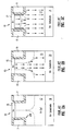
- FIG. 1 A cross-sectional view of a typical ACCUFET 10 is illustrated in FIG. 1.
- Trenched gates 11 are etched in a silicon material 12, which includes an N-epitaxial layer 13 grown on an N+ substrate 14.
- Trenched gates 11 are doped with N-type material and define two cells 10A and 10B.
- An N+ source 15 is formed at the top of the mesa between gates 11.
- a metal layer 16 is formed over the source regions, and a power source 17 and a load 18 are connected between the N+ source 15 and the N+ substrate 14, which acts as the drain.
- V GS the source voltage
- the epitaxial layer must be lightly doped (typically below 3 x 10 16 cm -3 ) and the channel must be long in comparison with the width of the mesa (typically less than 1.5 ⁇ m).
- V GS the depletion regions surrounding the gates (shown by the dashed lines) contract and open a current path between the source and the drain. With further increasing V GS the depletion regions continue to contract until eventually accumulation regions are formed adjacent the trenches, enhancing channel conduction and further lowering the on-resistance of the device.
- FIGS. 2A , 2B and 2C This sequence of events is illustrated in FIGS. 2A , 2B and 2C, FIG. 2A shows ACCUFET 10 in the off condition, FIG. 2B shows ACCUFET 10 turned partially on, and FIG. 2C shows ACCUFET 10 turned fully on, with the accumulation regions being designated by the numeral 19.
- the arrows represent the flow of electrons from the source to the drain.
- the region 11 A near the corner of the trench is where breakdown would occur, possibly causing damage to the gate oxide layer as a result of impact ionization and hot carrier injection into the gate oxide.
- ACCUFETs can tie fabricated with a very high cell density and a very low on-resistance. Despite these advantages, ACCUFETs have not so far achieved widespread use in the field of power semiconductor devices for several reasons. One of the principal reasons is that the leakage current in these devices is typically too high. Conversely, the long channel length and light epitaxial doping concentration required to reduce the leakage current produce a device that has a high on-resistance.
- a barrier accumulation-mode field-effect transistor (Barrier-ACCUFET) according to this invention fulfills this need.
- the Barrier-ACCUFET is fabricated in a semiconductor chip having first and second principal surfaces.
- a trench extends from the first surface of the semiconductor chip into the structure, the trench having first and second sections which define a mesa.
- a gate is disposed in the trench and insulated by a dielectric layer, typically an oxide, from the semiconductor chip, the gate being doped with ions of a first conductivity type.
- a source region of the first conductivity type is located in the mesa adjacent the first surface of the semiconductor chip.
- a body region of a second conductivity type is located in the mesa beneath the source region and adjacent the trench.
- a drain region of the first conductivity type is located beneath the body region.
- a drift region of the drain lies in the mesa between the gate trenches and may extend below the gate trenches. The drift region is typically doped more lightly than other portions of the drain.
- the net charge density in the body region is no greater than 1.5 x 10 12 cm -2 , measured with reference to a plane parallel to the top surface of the semiconductor and calculated as an integral of the net doping concentration in the body region between the source and drain junctions (i.e., each centimeter by centimeter "column" of the body region extending from the source to the drain contains no more than 1.5 x 10 12 ions).
- This in turn allows the dielectric (oxide) layer to be thicker and the threshold voltage to be lower than is possible in conventional MOSFETs.
- the body region can be shallow and the channel can be short, thereby reducing the on-resistance of the Barrier-ACCUFET.
- the body-drain junction is normally reverse-biased when the device is turned off and represents a barrier to the flow of current between the source and drain.
- the doping, concentration of ions of the first conductivity type in the gate, the thickness of the gate oxide layer, the dimensions of the mesa, and other parameters are such that the drift region in tile mesa is fully depleted when the device is turned off, impeding the flow of current between the source and drain regions.
- the net charge density of ions of the first conductivity type in the portion of the drift region between the trenches is no greater than 5 x 10 12 cm -2 , measured with reference to a plane perpendicular to the top surface of the semiconductor and calculated as an integral of the net doping concentration across the mesa from trench to trench (i.e., each centimeter by centimeter "column" of the drift region in the mesa, extending from the trench to trench, contains no more than 1.5 ⁇ 10 12 ions).
- This depletion region represents a second barrier to the flow of current between the source and drain. The body region therefore does not need to be doped as heavily as in prior art MOSFETs to prevent punchthrough behavior when the device is turned off.
- the depletion regions in the mesa shrink and an accumulation region is formed adjacent the trenches. This, combined with the short channel, reduces the on-resistance of the Barrier-ACCUFET.
- the semiconductor chip includes an epitaxial layer that is grown on a substrate.
- the substrate is typically doped more heavily than the epitaxial layer, and thus dopant diffuses some distance upward from the substrate into the epitaxial layer, creating a doping gradient at a level above the original interface between the substrate and the epitaxial layer.
- the trench extends into this gradient, although in other embodiments the trench bottom is located above the gradient.
- Fig. 1 is a cross-sectional view of a conventional accumulation-mode MOSFET (ACCUFET).
- ACCUFET accumulation-mode MOSFET
- Figs. 2A-2C illustrate the operation of the ACCUFET.
- Fig. 3 is a cross-sectional view of a conventional trench MOSFET.
- Fig. 4 is a cross-sectional view of a trench MOSFET with a deep diffusion which acts as a voltage clamp.
- Fig. 5 is a graph of the dopant profile of the source and body regions in a prior art MOSFET.
- Fig. 6A shows a cross-sectional view of a Barrier-ACCUFET according to this invention in an off condition.
- Fig. 6B shows a cross-sectional view of a Barrier-ACCUFET according to this invention in an intermediate condition between off and on.
- Fig. 6C shows a cross-sectional view of a Barrier-ACCUFET according to this invention in an on condition.
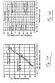
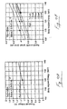
- Fig. 7A is a graph of the breakdown voltage of the Barrier-ACCUFET as a function of the thickness of the epitaxial layer.
- Fig. 7B is a graph of the specific on-resistance of the Barrier-ACCUFET as a function of the depth of the trench.
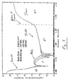
- Fig. 8 is a graph showing the doping profile of the Barrier-ACCUFET in a vertical cross-section.
- Fig. 9A is a graph of the threshold voltage of the Barrier-ACCUFET as a function of the energy used to implant the body region.
- Fig. 9B is a graph of the specific on-resistance of the Barrier-ACCUFET as a function of the energy used to implant the body region.
- Fig. 10 is a comparative graph of the specific on-resistance of Barrier-ACCUFETs and conventional MOSFETs having different gate oxide thicknesses as a function of the gate voltage.
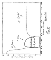
- Fig. 11 shows a top view of a Barrier-ACCUFET laid out in a stripe geometry.
- Fig. 12 illustrates various dimensions of a Barrier-ACCUFET.
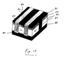
- Fig. 13 shows a Barrier-ACCUFET laid out in a modified stripe geometry which includes a clamping diode to limit the maximum drain-source voltage.
- Figs. 14A-14D show the steps of a process used to fabricated a Barrier-ACCUFET of this invention.
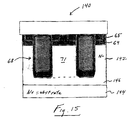
- Fig. 15 shows a Barrier-ACCUFET in which the trench does not extend entirely through the epitaxial layer or into the dopant gradient created by the; heavily doped substrate.
- FIG. 3 A cross-sectional view of a conventional trench MOSFET 30 is shown in Fig. 3.
- a gate 32 is formed in an epitaxial layer 34 over a substrate 36.
- Avalanche breakdown occurs at a comer of the trench designated 38.
- Fig. 4 shows a MOSFET 40 with a deep diffusion 42 of the kind taught in U.S. Patent No. 5,072,266 to Bulucea et al., which forms a "clamping diode".
- the MOSFET cell 46 shown in Fig. 4 is only one of numerous MOSFET cells that are formed in an array and together make up the entire power device.
- Patent No. 5,072,266 shows a deep diffusion in every MOSFET cell.
- the deep diffusions can be formed in separate "diode cells" that do not contain a channel and that are repeated in a pattern across the array of MOSFET cells, as taught in U.S. Patent No. 5,814,858 to Williams et al.
- the tip of the deep diffusion is preferably located at a level that is below the bottom of the trench. Even with the clamping diode, there is a critical thickness of the gate oxide layer below which the point of avalanche breakdown shifts back to the comer of the trench (see col. 10, lines 46-68 of U.S. Patent No. 5,072,266).
- Fig. 5 shows a graph of the dopant profile of the source and body regions in a prior art MOSFET, taken at a vertical cross-section in the vicinity of the channel region (see cross-section V-V in Fig. 3 ).
- the vertical axis is the log 10 of the dopant concentration in atoms/cm 3 ; the horizontal axis is the distance in ⁇ m below the surface of the semiconductor material.
- the width of the body region detennines the length of the channel region, which must be minimized for a low on-resistance R ds (on).
- the peak dopant concentration of the body region (10 17 cm -3 ) and the thickness of the gate oxide layer determine the threshold voltage V th .
- the net charge density of the body region (expressed as charge per unit area in a plane parallel to the surface of the semiconductor material) must be large enough to prevent punchthough.
- the prior art recognized that the net charge density in the body region must be at least 2 x 10 12 atoms/cm 2 (frequently abbreviated as cm -2 ) to ensure that punchthough does not occur.
- cm -2 the net charge density of the body region expressed as atoms/cm 2 or cm -2 refers to the number of charges in a vertical column measuring one centimeter by one centimeter extending through the entire depth of the body region. This is distinguished from the doping concentration, measured in atoms/cm 3 or simply cm -3 , which is the number of charges in a cubic centimeter of the semiconductor material.
- MOSFET 60 is formed in a semiconductor chip 69 which includes includes an epitaxial layer 62 and an N+ substrate 63.
- Epitaxial layer 62 includes a P-body region 64, an N+ source region 65 and a lightly doped N- drift region 66, which extends from the junction with P-body region 64 to the location where the doping concentration increases as a result of updiffusion from N+ substrate 63. This location is somewhat above the interface between epitaxial layer 62 and N+ substrate 63.
- N- drift region 66 and N+ substrate 63 are included within the drain of MOSFET 60.
- a metal layer 67 makes electrical contact with P-body region 64 and N+ source region 65.
- the N+ source region extends across the entire top surface of the mesa and the P-body region is contacted in the third dimension (see, e.g., Fig. 12 ).
- MOSFET 60 is typically connected in a circuit with a power source and a load in a way similar to MOSFET 10 as shown in Fig. 1 , so that a voltage difference is applied between the metal layer 67 and the N+ substrate 63 (drain) of MOSFET 60.
- a gate 61 is formed in a trench 68 that extends through epitaxial layer 62 and into N+ substrate 63. Gate 61 is separated from the semiconductor material by an oxide layer 70 P-body region 64 is shallow, defining a short channel having a length L ch between N+ source region 65 and N- drift region 66 adjacent the sidewall of the trench 68.
- trench 68 Two sections of trench 68 are shown and they define a mesa 72 of the semiconductor chip 69. There are many additional trench sections and mesas in the entire device, which is only partially shown in Figs. 6A-6C.
- the gate 61 is doped with an N-type material such as phosphorus.
- the electric field produced by the doped gate creates depletion regions, denoted by the dotted line 72 in Fig. 6A, in N- drift region 66.
- the depletion regions merge at the center of the mesa and effectively "pinch" the electric field in the mesa between the trenches, impeding the flow of current between the N+ source region 65 and the N+ substrate 63.
- the pinching of the electric field by the trench gate is used to shield the body region against the punchthrough effect.
- the body region can be made very shallow (e.g., a channel length less than 0.4 ⁇ m) while keeping the maximum body doping concentration below 1 x 10 17 cm -3 .
- the two-dimensional pinching effect caused by the electric field generated by the gate electrodes and the body-drain junction allows the net charge density in the body region to be lower than 1.5 x 10 12 cm -2 .
- the low doping concentration and net charge density in the body region allow the use of a relatively thick gate oxide layer (e.g., more than 250 ⁇ thick) while maintaining the threshold voltage at a low level (e.g., less than 1.2 V). This increases the maximum allowable gate-to-source voltage V GS(MAX) and lowers the gate capacitance, thereby increasing the switching speed of the device.
- the depletion regions surrounding the trench contract and, as shown in Fig. 6C , when the gate voltage is further increased, accumulation regions (denoted by the dotted lines 74) axe formed in the drift region 66 adjacent the trench 68. Also, as in a normal MOISFET the channel region of the P-body is inverted along the interface with the gate oxide. Thus a very low resistance current path between the source and the drain is formed through the short channel and the accumulation regions 74.
- the trenches extend through the epitaxial layer and at least into the doping gradient created by the updiffusion of dopant from the more heavily doped substrate, and the gate oxide layer is made thicker (e.g., more than 0.1 ⁇ m thick) at the bottom of the trench. This is particularly useful for devices having a maximum drain voltage of 10 V or more.
- the epitaxial layer can be doped uniformly, or the epitaxial layer can be graded, with a ratio between the doping concentration at the interface with the substrate to the doping concentration at the junction with the body region in the range of 3:1 to 7:1.
- Figs. 7A and 7B are graphs produced by computer simulations, using the MEDICI program, for a Barrier ACCUFET having a trench width of 0.8 ⁇ m and a mesa width of 1.2 ⁇ m, for a pitch of 2.0 ⁇ m.
- Fig. 7A shows the breakdown voltage of the device as a function of the thickness of the epitaxial layer ("epi-layer") for the following cases: (i) the doping concentration of the epi-layer (N epi ) equal to I x 10 16 cm -3 or 3 x 10 16 cm -3 and (ii) the thickness of the gate oxide layer at the bottom of the trench (TB OX ) equal to 0.1 ⁇ m or 0.3 ⁇ m.
- epi-layer the doping concentration of the epi-layer
- TB OX the thickness of the gate oxide layer at the bottom of the trench
- the results are shown for TB OX equal to 0.1 ⁇ m or 0.3 ⁇ m and the thickness of the epi-layer T epi equal to 2.0 ⁇ m or 2.5 ⁇ m.
- the doping gradient between the heavily doped substrate and the lightly doped drift region lies somewhat above the interface between the substrate and the epi-layer.
- the proper design of a Barrier-ACCUFET requires the trench to be deep enough to pinch the current in the mesa region effectively.
- the transition point between the dotted and solid lines in Fig. 7B indicates the minimum trench depth to prevent punchthrough behavior of the Barrier-ACCUFET.
- the epi-layer In order to minimize the on-resistance of the Barrier ACCUFET, the epi-layer should be made as thin as possible. A thicker epi-layer results in an excessive contribution of the epi-layer resistance to the total on-resistance of the device.
- the epi-layer can be less than 3 ⁇ m thick while still providing a breakdown voltage that is suitable for a 20 V device.
- Fig. 7B shows that the depth of the trench should be greater than 1.3 ⁇ m to prevent punchthrough behavior.
- the trench extends into the doping gradient in the epi-layer produced by the more heavily doped substrate. This allows full use of the additional current path through the accumulation layer adjacent the side walls of the trenches.
- the data provided above refer to a uniform doping profile in the epi-layer (i.e., the epi-layer before the formation of the body and source regions). Numerical simulations have also been performed to study the impact of a graded doping profile in the epi-layer on the performance of the device.
- the graded doping approach means there is a steady increase on the doping concentration in the epi-layer in the direction towards the heavily doped substrate.
- a linear doping profile in the epi-layer a flat, uniform electric field distribution can be achieved, as described in S. Merchant, IEEE Trans. on Electron Devices, Vol. 46, June 1999, pp. 1264-1267.
- a Gauss-like doping profile (linear on a logarithmic scale, as shown in Fig. 8 ) is preferable because it is easier to manufacture.
- a graded doping profile appears to be advantageous in terms of a reduced on-resistance of the device.
- the trench does extend into the doping gradient between the substrate and the epi-layer, as described above and as shown in Fig. 8, discussed below.
- This set of parameters results in a MOSFET having a breakdown voltage of 23 V and an on-resistance which depends on the body doping concentration and the gate oxide thickness, both of which determine the threshold voltage.
- Fig. 8 is a graph of the doping profile in the 20 V Barrier-ACCUFET in a vertical section through the channel region.
- the P body doping profile is shown for an implant close of 3.0 x 10 12 cm -2 at implant energies of 100 keV, 120 keV and 140 keV.
- the peak body doping concentration is in the range of 5 x 10 16 cm -3 .
- the body doping profile contains much less charge than in a conventional MOSFET design, and this results in a shorter channel (i.e., on the order of 0.4 ⁇ m).
- the N+ substrate (drain) has a doping concentration of about 2 x 10 19 cm -3 and the N+ source reaches a doping cocentration of about 2 x 10 20 cm -3 at the surface of the silicon.
- the drift region of the epi-layer Between the body region and the N+ substrate is the drift region of the epi-layer, wherein the doping concentration increases in a Gauss-like progression from about 7 x 10 15 cm -3 at the junction with the body to about 4 x 10 16 cm -3 where the gradient increases as a result of the influence of the N+ substrate (in this embodiment, also the level of the bottom of the trench).
- Fig. 9A shows the threshold voltage of the device as a function of the body implant energy at a gate oxide thickness of 500 ⁇ and a body implant dose of 2.5 x 10 12 cm -2 . As indicated, the threshold voltage can be less than 1.2 V even with a gate oxide as thick as 500 ⁇ . In order to avoid punchthrough under these conditions, the implant energy has to be at least about 120 keV, as indicated by the transition point between the dotted and solid lines. Fig.
- FIG. 9B shows the specific resistance RdsW per unit channel width (at a gate voltage of 4.5 V) as a function of the body implant energy for a device having the same gate oxide thickness and body implant dose.
- the trench width was held fixed at 0.8 ⁇ m and the pitch was varied from 1.6 ⁇ m to 2.4 ⁇ m.
- the mesa width varied from 0.8 ⁇ m to 1.6 ⁇ m. It is evident that decreasing the pitch from 2.4 ⁇ m to 2.0 ⁇ m permits the use of shallower body by decreasing the body implant energy from 140 keV to 120 keV without punchthrough. While a further decrease in the pitch to 1.6 ⁇ m would allow an even lower implant energy of 100 keV, a very small pitch is difficult to manufacture.
- the preferred parameters are as follows: Trench width 0.8 ⁇ m Mesa width 1.2 ⁇ m Body implant dose 2.5 x 10 12 cm -2 Body implant energy 120 keV
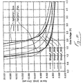
- Fig. 10 shows the specific resistance or a Barrier-ACCUFET as compared with the specific resistance of a conventional MOSFET. In both cases, the specific resistance per unit channel width is shown as a function of the gate voltage for specific gate oxide thicknesses. As indicated, about the same resistance can be achieved with almost double the gate oxide thickness.
- a 20 V Barrier-ACCUFET according to this invention with V GS(MAX) equal to ⁇ 12 V can have a gate oxide thickness of 300 ⁇ and a threshold voltage of only 0.6 V as shown in Fig. 10 . This result cannot be achieved using conventional MOSFET technology.
- the methodology described above for the design of a 20 V device is presented as an example and can be adapted to design devices having different voltage ratings.
- the Barrier-ACCUFET cells are laid out in a "stripe" configuration as shown in the top view of Fig. 11 .
- a closed cell configuration including, for example, square or hexagonal cells, can be used.
- Fig. 12 The following is a more generalized design process for manufacturing a Barrier-ACCUFET in a stripe geometry. Some of the dimensions referred to are illustrated in Fig. 12 .
- Computer-aided design tools allow the simultaneous optimization of the body, epi-layer and trench parameters and may be utilized once the interactions between these parameters are understood as described above and in the example.
- P+ regions 80 extend through the N+ source regions 82, the P-body regions 84 and the N- drift regions 86 to form a junction with the N+ substrate 88.
- the PN junction between P+ regions 80 and the N+ substrate 88 constitutes a clamping diode which limits V DS(MAX) and thereby prevents damage to the device.
- the separation between the P+ regions 80 can be less than 2.5 ⁇ m.
- Figs. 14A-14D illostrate a process of forming one embodiment of a Banier-ACCUFET according to this invention.
- the process begins with the growth of an N-epitaxial layer on an N+ silicon substrate and an initial oxidation of the top surface of the epitaxial layer.
- a first mask layer is formed to define the location of the deep diffusions that will form the clamping diodes, and dopant is implanted through openings in the first mask at a high energy.
- the P+ clamping diodes are implemented as stripes perpendicular to the trenches and diffused to reach the N+ substrate, as shown in Fig. 13 .
- a second mask layer is then formed over the initial oxidation layer with an opening which defines the active area of the device, and the initial oxidation layer is removed through an opening in the second mask layer.
- the second mask layer is removed, and a third mask layer is formed to define the locations of the trenches.
- the trenches are formed by a reactive ion etch (RIE) through openings in the third mask layer.
- RIE reactive ion etch
- a sacrificial oxide layer is formed in the walls and bottom of the trench and then etched to remove the silicon that was damaged by the RIE etch.
- the gate oxide layer is then formed thermally on the walls and bottom of the trench.
- the gate oxide layer is made thicker at the bottom of the trench. In one embodiment this is done by implanting ions vertically after the sacrificial oxide layer has been removed to damage the crystal structure of the silicon at the bottom of the trench.
- the ions implanted into the bottom of the trench should convert the crystalline material to an amorphous layer. To this end, the dose of the implanted ions should exceed a critical value known in the art as the threshold dose (see S. Wolf and R.N. Tauber, Silicon Processing For The VLSI Era, Vol. 1, page 302).
- argon ions are implanted with an energy of 100 keV and a dose higher than 4 x 10 14 ions/cm 2 .
- silicon ions are implanted at 100 keV with a dose higher than 5 x 10 14 ions/cm 2 . Because the ions are implanted vertically, they do not enter the sidewalls of the trench. This leads to a higher rate of oxidation at the bottom of the trench during the subsequent thermal process that forms the gate oxide.
- An N-epitaxial layer 102 overlies an N+ silicon substrate 100.
- Trenches 104 are formed in the epitaxial layer 102 and extend into the N+ substrate 100.
- a gate oxide layer 108 lines the walls of the trenches 104 and includes a thicker portion 110 at the bottoms of the trenches 104.
- trenches 104 are 0.8 ⁇ m wide and the mesas are 1.2 ⁇ m wide to yield a pitch of 2.0 ⁇ m.
- Trenches 104 can be 1.7 ⁇ m deep and the N+ substrate 100 and N-epitaxial layer 102 can have doping concentrations as shown in Fig. 8 .
- a polysilicon layer 112 is then deposited, filling trenches 104, and doped with N-type dopant to a concentration equal to or greater than 2 x 10 19 cm -3 .
- Polysilicon layer 112 call be doped with phosphorus by POCl 3 predisposition rind driven-in at 970 °C for 40 minutes, for example.
- a fourth mask layer is formed and polysilicon layer 112 is then etched back to a level coplanar with or slightly below the top surfaces of the mesas. The fourth mask layer is patterned such that gate runners are left connecting the trenches 104.
- An oxide layer 114 is then formed over the polysilicon layer 112 by a dry themal oxidation at 1050 °C for 10 minutes. The resulting structure is shown in Fig. 14B.
- P-type dopant (boron) is implanted to form a body region 116 (e.g., 2.5 x 10 12 cm -2 at 120 keV).
- N-type dopant is implanted at a dose of 5 ⁇ 10 15 cm -2 and an energy of 60 keV to form N+ source regions 118.
- a fifth mask layer can be formed to block the areas where contact is to be made to the body region 116 at the silicon surface. This leaves the structure shown in Fig. 14C .
- a layer 120 of borophosphosilicate glass (BSPG) is deposited on the top surface of the structure and reflowed.
- a sixth mask layer is formed over the BSPG layer 120 to define the openings where contact is to be made to the source regions 118 and the body regions 116.
- the BSPG layer 120 is then etched through the openings in the sixth mask layer, exposing the silicon in these areas.
- P-type dopant can be implanted at a dose of 1 x 10 15 cm -2 and an energy of 50 keV to form body contact regions at the surface of the silicon.
- the P-type dopant is not concentrated enough to affect the doping of the N+ source regions 118.
- the BSPG layer 120 is reflowed and a metal layer 122 is deposited, masked and etched, yielding the structure shown in Fig. 14D.
- Fig. 15 shows an embodiment which is similar to MOSFET 60 shown in Figs. 6A-6C , except that in MOSFET 140 the trench 68 does not extend all the way through the N- drift region 142 such that a portion of drift region 142 is interposed between the bottom of trench 68 and N+ substrate 144.
- the drift region 142 that is located in the mesa 71 is depleted when MOSFET 140 is turned off.
- dopant from the heavily doped N+ substrate 144 diffuses upward into the epi-layer 146 to form a dopant gradient within epi-layer 146.
Applications Claiming Priority (2)
| Application Number | Priority Date | Filing Date | Title |
|---|---|---|---|
| US476320 | 1999-12-30 | ||
| US09/476,320 US6285060B1 (en) | 1999-12-30 | 1999-12-30 | Barrier accumulation-mode MOSFET |
Publications (3)
| Publication Number | Publication Date |
|---|---|
| EP1113501A2 true EP1113501A2 (fr) | 2001-07-04 |
| EP1113501A3 EP1113501A3 (fr) | 2004-07-07 |
| EP1113501B1 EP1113501B1 (fr) | 2011-07-27 |
Family
ID=23891378
Family Applications (1)
| Application Number | Title | Priority Date | Filing Date |
|---|---|---|---|
| EP00128393A Expired - Lifetime EP1113501B1 (fr) | 1999-12-30 | 2000-12-22 | MOSFET de puissance à électrode de grille en tranchée |
Country Status (4)
| Country | Link |
|---|---|
| US (1) | US6285060B1 (fr) |
| EP (1) | EP1113501B1 (fr) |
| JP (1) | JP2001210822A (fr) |
| AT (1) | ATE518251T1 (fr) |
Cited By (4)
| Publication number | Priority date | Publication date | Assignee | Title |
|---|---|---|---|---|
| WO2003005414A3 (fr) * | 2001-07-05 | 2003-05-01 | Int Rectifier Corp | Tec a grille mos de puissance avec jonctions implantees profondement |
| EP1454360A1 (fr) * | 2001-11-21 | 2004-09-08 | GENERAL SEMICONDUCTOR, Inc. | Transistor mos a tranchee presentant une meilleure resistance a l'etat passant |
| CN105470255A (zh) * | 2014-09-30 | 2016-04-06 | 英飞凌科技股份有限公司 | 半导体器件及其制造方法 |
| CN113380882A (zh) * | 2020-03-09 | 2021-09-10 | 三菱电机株式会社 | 半导体装置 |
Families Citing this family (70)
| Publication number | Priority date | Publication date | Assignee | Title |
|---|---|---|---|---|
| JP2001085685A (ja) * | 1999-09-13 | 2001-03-30 | Shindengen Electric Mfg Co Ltd | トランジスタ |
| US6348712B1 (en) * | 1999-10-27 | 2002-02-19 | Siliconix Incorporated | High density trench-gated power MOSFET |
| GB0005650D0 (en) * | 2000-03-10 | 2000-05-03 | Koninkl Philips Electronics Nv | Field-effect semiconductor devices |
| US7745289B2 (en) | 2000-08-16 | 2010-06-29 | Fairchild Semiconductor Corporation | Method of forming a FET having ultra-low on-resistance and low gate charge |
| KR100338783B1 (en) * | 2000-10-28 | 2002-06-01 | Samsung Electronics Co Ltd | Semiconductor device having expanded effective width of active region and fabricating method thereof |
| US6803626B2 (en) | 2002-07-18 | 2004-10-12 | Fairchild Semiconductor Corporation | Vertical charge control semiconductor device |
| US6710403B2 (en) | 2002-07-30 | 2004-03-23 | Fairchild Semiconductor Corporation | Dual trench power MOSFET |
| US6870220B2 (en) * | 2002-08-23 | 2005-03-22 | Fairchild Semiconductor Corporation | Method and apparatus for improved MOS gating to reduce miller capacitance and switching losses |
| US6916745B2 (en) | 2003-05-20 | 2005-07-12 | Fairchild Semiconductor Corporation | Structure and method for forming a trench MOSFET having self-aligned features |
| US6818513B2 (en) | 2001-01-30 | 2004-11-16 | Fairchild Semiconductor Corporation | Method of forming a field effect transistor having a lateral depletion structure |
| JP2002270840A (ja) * | 2001-03-09 | 2002-09-20 | Toshiba Corp | パワーmosfet |
| JP2003046085A (ja) * | 2001-08-01 | 2003-02-14 | Seiko Epson Corp | 半導体装置及びその製造方法 |
| US6486511B1 (en) * | 2001-08-30 | 2002-11-26 | Northrop Grumman Corporation | Solid state RF switch with high cutoff frequency |
| GB0122122D0 (en) * | 2001-09-13 | 2001-10-31 | Koninkl Philips Electronics Nv | Trench-gate semiconductor devices and their manufacture |
| DE10262418B3 (de) * | 2002-02-21 | 2015-10-08 | Infineon Technologies Ag | MOS-Transistoreinrichtung |
| US6573561B1 (en) * | 2002-03-11 | 2003-06-03 | International Business Machines Corporation | Vertical MOSFET with asymmetrically graded channel doping |
| US7701001B2 (en) * | 2002-05-03 | 2010-04-20 | International Rectifier Corporation | Short channel trench power MOSFET with low threshold voltage |
| PL399493A1 (pl) * | 2002-05-10 | 2012-11-05 | F. Hoffmann-La Roche Ag | Kwasy bisfosfonowe do leczenia i profilaktyki osteoporozy |
| US7576388B1 (en) | 2002-10-03 | 2009-08-18 | Fairchild Semiconductor Corporation | Trench-gate LDMOS structures |
| US6710418B1 (en) | 2002-10-11 | 2004-03-23 | Fairchild Semiconductor Corporation | Schottky rectifier with insulation-filled trenches and method of forming the same |
| JP2004304155A (ja) * | 2003-03-19 | 2004-10-28 | Seiko Instruments Inc | 半導体装置の製造方法 |
| JP2004342863A (ja) * | 2003-05-16 | 2004-12-02 | Shindengen Electric Mfg Co Ltd | 半導体装置 |
| US7638841B2 (en) | 2003-05-20 | 2009-12-29 | Fairchild Semiconductor Corporation | Power semiconductor devices and methods of manufacture |
| GB0324313D0 (en) * | 2003-10-17 | 2003-11-19 | Koninkl Philips Electronics Nv | Trench insulated gate field effect transistor |
| KR100994719B1 (ko) | 2003-11-28 | 2010-11-16 | 페어차일드코리아반도체 주식회사 | 슈퍼정션 반도체장치 |
| DE10355588B4 (de) * | 2003-11-28 | 2006-06-14 | Infineon Technologies Ag | MOS-Transistoreinrichtung |
| US7368777B2 (en) | 2003-12-30 | 2008-05-06 | Fairchild Semiconductor Corporation | Accumulation device with charge balance structure and method of forming the same |
| JP2005302925A (ja) * | 2004-04-09 | 2005-10-27 | Toshiba Corp | 半導体装置 |
| US7352036B2 (en) | 2004-08-03 | 2008-04-01 | Fairchild Semiconductor Corporation | Semiconductor power device having a top-side drain using a sinker trench |
| KR100712989B1 (ko) | 2005-03-14 | 2007-05-02 | 주식회사 하이닉스반도체 | 리세스 채널 및 비대칭접합 구조를 갖는 반도체 소자의제조방법 |
| DE102005014743B4 (de) * | 2005-03-31 | 2013-12-05 | Infineon Technologies Austria Ag | MOS-Feldplattentrench-Transistoreinrichtung |
| DE102005014744B4 (de) | 2005-03-31 | 2009-06-18 | Infineon Technologies Ag | Trenchtransistor mit erhöhter Avalanchefestigkeit und Herstellungsverfahren |
| DE112006000832B4 (de) | 2005-04-06 | 2018-09-27 | Fairchild Semiconductor Corporation | Trenched-Gate-Feldeffekttransistoren und Verfahren zum Bilden derselben |
| DE112006001516T5 (de) | 2005-06-10 | 2008-04-17 | Fairchild Semiconductor Corp. | Feldeffekttransistor mit Ladungsgleichgewicht |
| US7385248B2 (en) * | 2005-08-09 | 2008-06-10 | Fairchild Semiconductor Corporation | Shielded gate field effect transistor with improved inter-poly dielectric |
| US7446374B2 (en) | 2006-03-24 | 2008-11-04 | Fairchild Semiconductor Corporation | High density trench FET with integrated Schottky diode and method of manufacture |
| US7319256B1 (en) | 2006-06-19 | 2008-01-15 | Fairchild Semiconductor Corporation | Shielded gate trench FET with the shield and gate electrodes being connected together |
| US9437729B2 (en) * | 2007-01-08 | 2016-09-06 | Vishay-Siliconix | High-density power MOSFET with planarized metalization |
| US9947770B2 (en) * | 2007-04-03 | 2018-04-17 | Vishay-Siliconix | Self-aligned trench MOSFET and method of manufacture |
| CN101868856B (zh) | 2007-09-21 | 2014-03-12 | 飞兆半导体公司 | 用于功率器件的超结结构及制造方法 |
| US9484451B2 (en) | 2007-10-05 | 2016-11-01 | Vishay-Siliconix | MOSFET active area and edge termination area charge balance |
| US7772668B2 (en) | 2007-12-26 | 2010-08-10 | Fairchild Semiconductor Corporation | Shielded gate trench FET with multiple channels |
| WO2009119479A1 (fr) * | 2008-03-24 | 2009-10-01 | 日本電気株式会社 | Dispositif à semi-conducteur et son procédé de fabrication |
| US20120273916A1 (en) | 2011-04-27 | 2012-11-01 | Yedinak Joseph A | Superjunction Structures for Power Devices and Methods of Manufacture |
| US8426275B2 (en) | 2009-01-09 | 2013-04-23 | Niko Semiconductor Co., Ltd. | Fabrication method of trenched power MOSFET |
| TWI435447B (zh) * | 2009-01-09 | 2014-04-21 | Niko Semiconductor Co Ltd | 功率金氧半導體場效電晶體及其製造方法 |
| US7989293B2 (en) * | 2009-02-24 | 2011-08-02 | Maxpower Semiconductor, Inc. | Trench device structure and fabrication |
| US9443974B2 (en) | 2009-08-27 | 2016-09-13 | Vishay-Siliconix | Super junction trench power MOSFET device fabrication |
| US9431530B2 (en) * | 2009-10-20 | 2016-08-30 | Vishay-Siliconix | Super-high density trench MOSFET |
| US10026835B2 (en) | 2009-10-28 | 2018-07-17 | Vishay-Siliconix | Field boosted metal-oxide-semiconductor field effect transistor |
| US8129778B2 (en) * | 2009-12-02 | 2012-03-06 | Fairchild Semiconductor Corporation | Semiconductor devices and methods for making the same |
| US20110198689A1 (en) * | 2010-02-17 | 2011-08-18 | Suku Kim | Semiconductor devices containing trench mosfets with superjunctions |
| US8432000B2 (en) | 2010-06-18 | 2013-04-30 | Fairchild Semiconductor Corporation | Trench MOS barrier schottky rectifier with a planar surface using CMP techniques |
| JP2012204636A (ja) * | 2011-03-25 | 2012-10-22 | Toshiba Corp | 半導体装置およびその製造方法 |
| US8772868B2 (en) | 2011-04-27 | 2014-07-08 | Fairchild Semiconductor Corporation | Superjunction structures for power devices and methods of manufacture |
| US8786010B2 (en) | 2011-04-27 | 2014-07-22 | Fairchild Semiconductor Corporation | Superjunction structures for power devices and methods of manufacture |
| US8673700B2 (en) | 2011-04-27 | 2014-03-18 | Fairchild Semiconductor Corporation | Superjunction structures for power devices and methods of manufacture |
| US8836028B2 (en) | 2011-04-27 | 2014-09-16 | Fairchild Semiconductor Corporation | Superjunction structures for power devices and methods of manufacture |
| US10164043B2 (en) * | 2012-01-11 | 2018-12-25 | Infineon Technologies Ag | Semiconductor diode and method for forming a semiconductor diode |
| US9842911B2 (en) | 2012-05-30 | 2017-12-12 | Vishay-Siliconix | Adaptive charge balanced edge termination |
| US9508596B2 (en) | 2014-06-20 | 2016-11-29 | Vishay-Siliconix | Processes used in fabricating a metal-insulator-semiconductor field effect transistor |
| US9887259B2 (en) | 2014-06-23 | 2018-02-06 | Vishay-Siliconix | Modulated super junction power MOSFET devices |
| EP3183754A4 (fr) | 2014-08-19 | 2018-05-02 | Vishay-Siliconix | Transistor à effet de champ à semi-conducteur d'oxyde de métal à super jonction |
| CN107078161A (zh) | 2014-08-19 | 2017-08-18 | 维西埃-硅化物公司 | 电子电路 |
| US9577073B2 (en) * | 2014-12-11 | 2017-02-21 | Infineon Technologies Ag | Method of forming a silicon-carbide device with a shielded gate |
| DE102015208097B4 (de) * | 2015-04-30 | 2022-03-31 | Infineon Technologies Ag | Herstellen einer Halbleitervorrichtung durch Epitaxie |
| DE102016109555A1 (de) * | 2016-05-24 | 2017-11-30 | Infineon Technologies Austria Ag | Leistungshalbleiterbauelement und verfahren zur herstellung eines leistungshalbleiterbauelements |
| DE102017118352A1 (de) * | 2017-08-11 | 2019-02-14 | Infineon Technologies Ag | Halbleiterbauelement mit grabenstrukturen und herstellungsverfahren hierfür |
| JP2019046991A (ja) * | 2017-09-04 | 2019-03-22 | ルネサスエレクトロニクス株式会社 | 半導体装置およびその製造方法 |
| US10847617B2 (en) | 2017-12-14 | 2020-11-24 | Fuji Electric Co., Ltd. | Semiconductor device |
Citations (3)
| Publication number | Priority date | Publication date | Assignee | Title |
|---|---|---|---|---|
| US4903189A (en) | 1988-04-27 | 1990-02-20 | General Electric Company | Low noise, high frequency synchronous rectifier |
| US5072266A (en) | 1988-12-27 | 1991-12-10 | Siliconix Incorporated | Trench DMOS power transistor with field-shaping body profile and three-dimensional geometry |
| US5814838A (en) | 1996-05-22 | 1998-09-29 | Sanken Electric Co., Ltd. | Light emitting semiconductor element with ZN doping |
Family Cites Families (13)
| Publication number | Priority date | Publication date | Assignee | Title |
|---|---|---|---|---|
| US4364072A (en) * | 1978-03-17 | 1982-12-14 | Zaidan Hojin Handotai Kenkyu Shinkokai | Static induction type semiconductor device with multiple doped layers for potential modification |
| US4941026A (en) * | 1986-12-05 | 1990-07-10 | General Electric Company | Semiconductor devices exhibiting minimum on-resistance |
| JPH045A (ja) * | 1990-04-17 | 1992-01-06 | Takashi Kimura | 空気シリンダにおけるピストンロッドの減速制御方法 |
| US5326711A (en) * | 1993-01-04 | 1994-07-05 | Texas Instruments Incorporated | High performance high voltage vertical transistor and method of fabrication |
| US5405794A (en) * | 1994-06-14 | 1995-04-11 | Philips Electronics North America Corporation | Method of producing VDMOS device of increased power density |
| US5688725A (en) * | 1994-12-30 | 1997-11-18 | Siliconix Incorporated | Method of making a trench mosfet with heavily doped delta layer to provide low on-resistance |
| US5592005A (en) * | 1995-03-31 | 1997-01-07 | Siliconix Incorporated | Punch-through field effect transistor |
| US5637898A (en) * | 1995-12-22 | 1997-06-10 | North Carolina State University | Vertical field effect transistors having improved breakdown voltage capability and low on-state resistance |
| US5814858A (en) * | 1996-03-15 | 1998-09-29 | Siliconix Incorporated | Vertical power MOSFET having reduced sensitivity to variations in thickness of epitaxial layer |
| JP3505039B2 (ja) * | 1996-07-12 | 2004-03-08 | 株式会社ルネサステクノロジ | 半導体装置及びその製造方法 |
| US6090716A (en) * | 1996-12-17 | 2000-07-18 | Siliconix Incorporated | Method of fabricating a field effect transistor |
| JPH10256550A (ja) * | 1997-01-09 | 1998-09-25 | Toshiba Corp | 半導体装置 |
| GB9808234D0 (en) * | 1998-04-17 | 1998-06-17 | Koninkl Philips Electronics Nv | Mnufacture of trench-gate semiconductor devices |
-
1999
- 1999-12-30 US US09/476,320 patent/US6285060B1/en not_active Expired - Lifetime
-
2000
- 2000-12-22 EP EP00128393A patent/EP1113501B1/fr not_active Expired - Lifetime
- 2000-12-22 AT AT00128393T patent/ATE518251T1/de not_active IP Right Cessation
- 2000-12-26 JP JP2000395089A patent/JP2001210822A/ja active Pending
Patent Citations (3)
| Publication number | Priority date | Publication date | Assignee | Title |
|---|---|---|---|---|
| US4903189A (en) | 1988-04-27 | 1990-02-20 | General Electric Company | Low noise, high frequency synchronous rectifier |
| US5072266A (en) | 1988-12-27 | 1991-12-10 | Siliconix Incorporated | Trench DMOS power transistor with field-shaping body profile and three-dimensional geometry |
| US5814838A (en) | 1996-05-22 | 1998-09-29 | Sanken Electric Co., Ltd. | Light emitting semiconductor element with ZN doping |
Non-Patent Citations (2)
| Title |
|---|
| B. J. BALIGA ET AL.: "The Accumulation-Mode Field-Effect Transistor: A New Ultralow On-Resistance MOSFET", IEEE ELECTRON DEVICE LETTERS, vol. 13, no. 8, August 1992 (1992-08-01), pages 427 - 429 |
| T. SYAU ET AL.: "Comparison of Ultralow Specific On-Resistance UMOSFET Structures: The ACCUFET, EXTFET, INVFET, and Conventional UMOSFET's", IEEE ELECTRON DEVICE LETTERS, vol. 41, no. 5, May 1994 (1994-05-01), pages 800 - 808 |
Cited By (8)
| Publication number | Priority date | Publication date | Assignee | Title |
|---|---|---|---|---|
| WO2003005414A3 (fr) * | 2001-07-05 | 2003-05-01 | Int Rectifier Corp | Tec a grille mos de puissance avec jonctions implantees profondement |
| US6639276B2 (en) | 2001-07-05 | 2003-10-28 | International Rectifier Corporation | Power MOSFET with ultra-deep base and reduced on resistance |
| CN1333468C (zh) * | 2001-07-05 | 2007-08-22 | 国际整流器有限公司 | 具有深植入结的功率mosfet |
| EP1454360A1 (fr) * | 2001-11-21 | 2004-09-08 | GENERAL SEMICONDUCTOR, Inc. | Transistor mos a tranchee presentant une meilleure resistance a l'etat passant |
| EP1454360A4 (fr) * | 2001-11-21 | 2008-12-17 | Gen Semiconductor Inc | Transistor mos a tranchee presentant une meilleure resistance a l'etat passant |
| CN105470255A (zh) * | 2014-09-30 | 2016-04-06 | 英飞凌科技股份有限公司 | 半导体器件及其制造方法 |
| CN105470255B (zh) * | 2014-09-30 | 2020-08-18 | 英飞凌科技股份有限公司 | 半导体器件及其制造方法 |
| CN113380882A (zh) * | 2020-03-09 | 2021-09-10 | 三菱电机株式会社 | 半导体装置 |
Also Published As
| Publication number | Publication date |
|---|---|
| EP1113501B1 (fr) | 2011-07-27 |
| JP2001210822A (ja) | 2001-08-03 |
| US6285060B1 (en) | 2001-09-04 |
| EP1113501A3 (fr) | 2004-07-07 |
| ATE518251T1 (de) | 2011-08-15 |
Similar Documents
| Publication | Publication Date | Title |
|---|---|---|
| US6285060B1 (en) | Barrier accumulation-mode MOSFET | |
| US7427800B2 (en) | Semiconductor device containing dielectrically isolated PN junction for enhanced breakdown characteristics | |
| KR100628938B1 (ko) | 개선된 고주파 스위칭 특성 및 항복 특성을 갖는 전력용반도체 장치들 | |
| US6764889B2 (en) | Methods of forming vertical mosfets having trench-based gate electrodes within deeper trench-based source electrodes | |
| US6825105B2 (en) | Manufacture of semiconductor devices with Schottky barriers | |
| US8466025B2 (en) | Semiconductor device structures and related processes | |
| US6849880B1 (en) | Power semiconductor device | |
| US6049108A (en) | Trench-gated MOSFET with bidirectional voltage clamping | |
| US6444527B1 (en) | Method of operation of punch-through field effect transistor | |
| US6566708B1 (en) | Trench-gate field-effect transistors with low gate-drain capacitance and their manufacture | |
| US6218228B1 (en) | DMOS device structure, and related manufacturing process | |
| US10211333B2 (en) | Scalable SGT structure with improved FOM | |
| US9147751B2 (en) | Methods of manufacturing superjunction devices | |
| CN115863438A (zh) | 具有分离平面栅结构的金属氧化物半导体场效应晶体管 | |
| US20080272429A1 (en) | Superjunction devices having narrow surface layout of terminal structures and methods of manufacturing the devices | |
| JP2004537162A (ja) | パワーデバイスとその製造方法 | |
| KR100381845B1 (ko) | 트렌치-게이트형파워mosfet | |
| CN116031303B (zh) | 超结器件及其制作方法和电子器件 | |
| CN115188812A (zh) | 具有分离平面栅结构的金属氧化物半导体场效应晶体管 | |
| US20230163167A1 (en) | Semiconductor device including a trench gate structure |
Legal Events
| Date | Code | Title | Description |
|---|---|---|---|
| PUAI | Public reference made under article 153(3) epc to a published international application that has entered the european phase |
Free format text: ORIGINAL CODE: 0009012 |
|
| AK | Designated contracting states |
Kind code of ref document: A2 Designated state(s): AT BE CH CY DE DK ES FI FR GB GR IE IT LI LU MC NL PT SE TR |
|
| AX | Request for extension of the european patent |
Free format text: AL;LT;LV;MK;RO;SI |
|
| RIC1 | Information provided on ipc code assigned before grant |
Ipc: 7H 01L 29/78 A |
|
| PUAL | Search report despatched |
Free format text: ORIGINAL CODE: 0009013 |
|
| AK | Designated contracting states |
Kind code of ref document: A3 Designated state(s): AT BE CH CY DE DK ES FI FR GB GR IE IT LI LU MC NL PT SE TR |
|
| AX | Request for extension of the european patent |
Extension state: AL LT LV MK RO SI |
|
| 17P | Request for examination filed |
Effective date: 20041028 |
|
| AKX | Designation fees paid |
Designated state(s): AT BE CH CY DE DK ES FI FR GB GR IE IT LI LU MC NL PT SE TR |
|
| R17C | First examination report despatched (corrected) |
Effective date: 20061215 |
|
| RIC1 | Information provided on ipc code assigned before grant |
Ipc: H01L 29/10 20060101ALN20101110BHEP Ipc: H01L 29/06 20060101ALN20101110BHEP Ipc: H01L 29/49 20060101ALN20101110BHEP Ipc: H01L 29/78 20060101AFI20101110BHEP Ipc: H01L 29/08 20060101ALN20101110BHEP Ipc: H01L 29/423 20060101ALN20101110BHEP |
|
| GRAP | Despatch of communication of intention to grant a patent |
Free format text: ORIGINAL CODE: EPIDOSNIGR1 |
|
| GRAS | Grant fee paid |
Free format text: ORIGINAL CODE: EPIDOSNIGR3 |
|
| GRAA | (expected) grant |
Free format text: ORIGINAL CODE: 0009210 |
|
| AK | Designated contracting states |
Kind code of ref document: B1 Designated state(s): AT BE CH CY DE DK ES FI FR GB GR IE IT LI LU MC NL PT SE TR |
|
| REG | Reference to a national code |
Ref country code: GB Ref legal event code: FG4D |
|
| REG | Reference to a national code |
Ref country code: CH Ref legal event code: EP |
|
| REG | Reference to a national code |
Ref country code: DE Ref legal event code: R096 Ref document number: 60046258 Country of ref document: DE Effective date: 20110915 |
|
| REG | Reference to a national code |
Ref country code: NL Ref legal event code: VDEP Effective date: 20110727 |
|
| REG | Reference to a national code |
Ref country code: AT Ref legal event code: MK05 Ref document number: 518251 Country of ref document: AT Kind code of ref document: T Effective date: 20110727 |
|
| PG25 | Lapsed in a contracting state [announced via postgrant information from national office to epo] |
Ref country code: SE Free format text: LAPSE BECAUSE OF FAILURE TO SUBMIT A TRANSLATION OF THE DESCRIPTION OR TO PAY THE FEE WITHIN THE PRESCRIBED TIME-LIMIT Effective date: 20110727 Ref country code: BE Free format text: LAPSE BECAUSE OF FAILURE TO SUBMIT A TRANSLATION OF THE DESCRIPTION OR TO PAY THE FEE WITHIN THE PRESCRIBED TIME-LIMIT Effective date: 20110727 Ref country code: FI Free format text: LAPSE BECAUSE OF FAILURE TO SUBMIT A TRANSLATION OF THE DESCRIPTION OR TO PAY THE FEE WITHIN THE PRESCRIBED TIME-LIMIT Effective date: 20110727 Ref country code: NL Free format text: LAPSE BECAUSE OF FAILURE TO SUBMIT A TRANSLATION OF THE DESCRIPTION OR TO PAY THE FEE WITHIN THE PRESCRIBED TIME-LIMIT Effective date: 20110727 Ref country code: PT Free format text: LAPSE BECAUSE OF FAILURE TO SUBMIT A TRANSLATION OF THE DESCRIPTION OR TO PAY THE FEE WITHIN THE PRESCRIBED TIME-LIMIT Effective date: 20111128 |
|
| PG25 | Lapsed in a contracting state [announced via postgrant information from national office to epo] |
Ref country code: GR Free format text: LAPSE BECAUSE OF FAILURE TO SUBMIT A TRANSLATION OF THE DESCRIPTION OR TO PAY THE FEE WITHIN THE PRESCRIBED TIME-LIMIT Effective date: 20111028 Ref country code: CY Free format text: LAPSE BECAUSE OF FAILURE TO SUBMIT A TRANSLATION OF THE DESCRIPTION OR TO PAY THE FEE WITHIN THE PRESCRIBED TIME-LIMIT Effective date: 20110727 Ref country code: AT Free format text: LAPSE BECAUSE OF FAILURE TO SUBMIT A TRANSLATION OF THE DESCRIPTION OR TO PAY THE FEE WITHIN THE PRESCRIBED TIME-LIMIT Effective date: 20110727 |
|
| PLBE | No opposition filed within time limit |
Free format text: ORIGINAL CODE: 0009261 |
|
| STAA | Information on the status of an ep patent application or granted ep patent |
Free format text: STATUS: NO OPPOSITION FILED WITHIN TIME LIMIT |
|
| PG25 | Lapsed in a contracting state [announced via postgrant information from national office to epo] |
Ref country code: DK Free format text: LAPSE BECAUSE OF FAILURE TO SUBMIT A TRANSLATION OF THE DESCRIPTION OR TO PAY THE FEE WITHIN THE PRESCRIBED TIME-LIMIT Effective date: 20110727 |
|
| 26N | No opposition filed |
Effective date: 20120502 |
|
| PG25 | Lapsed in a contracting state [announced via postgrant information from national office to epo] |
Ref country code: MC Free format text: LAPSE BECAUSE OF NON-PAYMENT OF DUE FEES Effective date: 20111231 |
|
| REG | Reference to a national code |
Ref country code: CH Ref legal event code: PL |
|
| REG | Reference to a national code |
Ref country code: DE Ref legal event code: R097 Ref document number: 60046258 Country of ref document: DE Effective date: 20120502 |
|
| REG | Reference to a national code |
Ref country code: IE Ref legal event code: MM4A |
|
| PG25 | Lapsed in a contracting state [announced via postgrant information from national office to epo] |
Ref country code: CH Free format text: LAPSE BECAUSE OF NON-PAYMENT OF DUE FEES Effective date: 20111231 Ref country code: LI Free format text: LAPSE BECAUSE OF NON-PAYMENT OF DUE FEES Effective date: 20111231 Ref country code: IE Free format text: LAPSE BECAUSE OF NON-PAYMENT OF DUE FEES Effective date: 20111222 |
|
| PG25 | Lapsed in a contracting state [announced via postgrant information from national office to epo] |
Ref country code: ES Free format text: LAPSE BECAUSE OF FAILURE TO SUBMIT A TRANSLATION OF THE DESCRIPTION OR TO PAY THE FEE WITHIN THE PRESCRIBED TIME-LIMIT Effective date: 20111107 |
|
| PG25 | Lapsed in a contracting state [announced via postgrant information from national office to epo] |
Ref country code: LU Free format text: LAPSE BECAUSE OF NON-PAYMENT OF DUE FEES Effective date: 20111222 |
|
| PG25 | Lapsed in a contracting state [announced via postgrant information from national office to epo] |
Ref country code: TR Free format text: LAPSE BECAUSE OF FAILURE TO SUBMIT A TRANSLATION OF THE DESCRIPTION OR TO PAY THE FEE WITHIN THE PRESCRIBED TIME-LIMIT Effective date: 20110727 |
|
| REG | Reference to a national code |
Ref country code: FR Ref legal event code: PLFP Year of fee payment: 16 |
|
| PGFP | Annual fee paid to national office [announced via postgrant information from national office to epo] |
Ref country code: GB Payment date: 20151229 Year of fee payment: 16 |
|
| PGFP | Annual fee paid to national office [announced via postgrant information from national office to epo] |
Ref country code: FR Payment date: 20151217 Year of fee payment: 16 |
|
| PGFP | Annual fee paid to national office [announced via postgrant information from national office to epo] |
Ref country code: DE Payment date: 20151229 Year of fee payment: 16 |
|
| PG25 | Lapsed in a contracting state [announced via postgrant information from national office to epo] |
Ref country code: IT Free format text: LAPSE BECAUSE OF NON-PAYMENT OF DUE FEES Effective date: 20151222 |
|
| REG | Reference to a national code |
Ref country code: DE Ref legal event code: R119 Ref document number: 60046258 Country of ref document: DE |
|
| GBPC | Gb: european patent ceased through non-payment of renewal fee |
Effective date: 20161222 |
|
| PG25 | Lapsed in a contracting state [announced via postgrant information from national office to epo] |
Ref country code: IT Free format text: LAPSE BECAUSE OF NON-PAYMENT OF DUE FEES Effective date: 20151222 |
|
| PGFP | Annual fee paid to national office [announced via postgrant information from national office to epo] |
Ref country code: IT Payment date: 20151222 Year of fee payment: 16 |
|
| PGRI | Patent reinstated in contracting state [announced from national office to epo] |
Ref country code: IT Effective date: 20170710 |
|
| REG | Reference to a national code |
Ref country code: FR Ref legal event code: ST Effective date: 20170831 |
|
| PG25 | Lapsed in a contracting state [announced via postgrant information from national office to epo] |
Ref country code: FR Free format text: LAPSE BECAUSE OF NON-PAYMENT OF DUE FEES Effective date: 20170102 Ref country code: IT Free format text: LAPSE BECAUSE OF NON-PAYMENT OF DUE FEES Effective date: 20161222 |
|
| PGRI | Patent reinstated in contracting state [announced from national office to epo] |
Ref country code: IT Effective date: 20170710 |
|
| PG25 | Lapsed in a contracting state [announced via postgrant information from national office to epo] |
Ref country code: GB Free format text: LAPSE BECAUSE OF NON-PAYMENT OF DUE FEES Effective date: 20161222 Ref country code: DE Free format text: LAPSE BECAUSE OF NON-PAYMENT OF DUE FEES Effective date: 20170701 |