EP1107064A2 - Belichtungsapparat - Google Patents
Belichtungsapparat Download PDFInfo
- Publication number
- EP1107064A2 EP1107064A2 EP00125392A EP00125392A EP1107064A2 EP 1107064 A2 EP1107064 A2 EP 1107064A2 EP 00125392 A EP00125392 A EP 00125392A EP 00125392 A EP00125392 A EP 00125392A EP 1107064 A2 EP1107064 A2 EP 1107064A2
- Authority
- EP
- European Patent Office
- Prior art keywords
- exposure
- substrate
- image
- exposure apparatus
- circuit pattern
- Prior art date
- Legal status (The legal status is an assumption and is not a legal conclusion. Google has not performed a legal analysis and makes no representation as to the accuracy of the status listed.)
- Withdrawn
Links
Images


Classifications
-
- G—PHYSICS
- G03—PHOTOGRAPHY; CINEMATOGRAPHY; ANALOGOUS TECHNIQUES USING WAVES OTHER THAN OPTICAL WAVES; ELECTROGRAPHY; HOLOGRAPHY
- G03F—PHOTOMECHANICAL PRODUCTION OF TEXTURED OR PATTERNED SURFACES, e.g. FOR PRINTING, FOR PROCESSING OF SEMICONDUCTOR DEVICES; MATERIALS THEREFOR; ORIGINALS THEREFOR; APPARATUS SPECIALLY ADAPTED THEREFOR
- G03F7/00—Photomechanical, e.g. photolithographic, production of textured or patterned surfaces, e.g. printing surfaces; Materials therefor, e.g. comprising photoresists; Apparatus specially adapted therefor
- G03F7/70—Microphotolithographic exposure; Apparatus therefor
- G03F7/70216—Mask projection systems
- G03F7/70275—Multiple projection paths, e.g. array of projection systems, microlens projection systems or tandem projection systems
-
- G—PHYSICS
- G03—PHOTOGRAPHY; CINEMATOGRAPHY; ANALOGOUS TECHNIQUES USING WAVES OTHER THAN OPTICAL WAVES; ELECTROGRAPHY; HOLOGRAPHY
- G03F—PHOTOMECHANICAL PRODUCTION OF TEXTURED OR PATTERNED SURFACES, e.g. FOR PRINTING, FOR PROCESSING OF SEMICONDUCTOR DEVICES; MATERIALS THEREFOR; ORIGINALS THEREFOR; APPARATUS SPECIALLY ADAPTED THEREFOR
- G03F7/00—Photomechanical, e.g. photolithographic, production of textured or patterned surfaces, e.g. printing surfaces; Materials therefor, e.g. comprising photoresists; Apparatus specially adapted therefor
- G03F7/70—Microphotolithographic exposure; Apparatus therefor
- G03F7/70425—Imaging strategies, e.g. for increasing throughput or resolution, printing product fields larger than the image field or compensating lithography- or non-lithography errors, e.g. proximity correction, mix-and-match, stitching or double patterning
- G03F7/70475—Stitching, i.e. connecting image fields to produce a device field, the field occupied by a device such as a memory chip, processor chip, CCD, flat panel display
-
- G—PHYSICS
- G03—PHOTOGRAPHY; CINEMATOGRAPHY; ANALOGOUS TECHNIQUES USING WAVES OTHER THAN OPTICAL WAVES; ELECTROGRAPHY; HOLOGRAPHY
- G03F—PHOTOMECHANICAL PRODUCTION OF TEXTURED OR PATTERNED SURFACES, e.g. FOR PRINTING, FOR PROCESSING OF SEMICONDUCTOR DEVICES; MATERIALS THEREFOR; ORIGINALS THEREFOR; APPARATUS SPECIALLY ADAPTED THEREFOR
- G03F7/00—Photomechanical, e.g. photolithographic, production of textured or patterned surfaces, e.g. printing surfaces; Materials therefor, e.g. comprising photoresists; Apparatus specially adapted therefor
- G03F7/70—Microphotolithographic exposure; Apparatus therefor
- G03F7/70691—Handling of masks or workpieces
- G03F7/70791—Large workpieces, e.g. glass substrates for flat panel displays or solar panels
-
- G—PHYSICS
- G03—PHOTOGRAPHY; CINEMATOGRAPHY; ANALOGOUS TECHNIQUES USING WAVES OTHER THAN OPTICAL WAVES; ELECTROGRAPHY; HOLOGRAPHY
- G03F—PHOTOMECHANICAL PRODUCTION OF TEXTURED OR PATTERNED SURFACES, e.g. FOR PRINTING, FOR PROCESSING OF SEMICONDUCTOR DEVICES; MATERIALS THEREFOR; ORIGINALS THEREFOR; APPARATUS SPECIALLY ADAPTED THEREFOR
- G03F7/00—Photomechanical, e.g. photolithographic, production of textured or patterned surfaces, e.g. printing surfaces; Materials therefor, e.g. comprising photoresists; Apparatus specially adapted therefor
- G03F7/70—Microphotolithographic exposure; Apparatus therefor
- G03F7/708—Construction of apparatus, e.g. environment aspects, hygiene aspects or materials
- G03F7/70991—Connection with other apparatus, e.g. multiple exposure stations, particular arrangement of exposure apparatus and pre-exposure and/or post-exposure apparatus; Shared apparatus, e.g. having shared radiation source, shared mask or workpiece stage, shared base-plate; Utilities, e.g. cable, pipe or wireless arrangements for data, power, fluids or vacuum
-
- H—ELECTRICITY
- H04—ELECTRIC COMMUNICATION TECHNIQUE
- H04N—PICTORIAL COMMUNICATION, e.g. TELEVISION
- H04N9/00—Details of colour television systems
- H04N9/12—Picture reproducers
- H04N9/31—Projection devices for colour picture display, e.g. using electronic spatial light modulators [ESLM]
- H04N9/3141—Constructional details thereof
- H04N9/3147—Multi-projection systems
Definitions
- the present invention relates to an exposure apparatus and, more particularly, to an exposure apparatus for exposing a circuit pattern of a semiconductor device, liquid crystal display device, etc. to a prescribed substrate, etc.
- the invention concerns an exposure apparatus for exposing a prescribed circuit pattern, etc. to a prescribed substrate, etc. in order to manufacture a high-density print circuit substrate of a BGA substrate, CSP substrate, etc.
- An exposure apparatus for optically exposing a circuit pattern of a semiconductor device, liquid crystal display device, etc., which is what is called “a stepper”, has hitherto been generally put to practical use.
- An ordinary exposure apparatus is generally constructed in such a form wherein, for example, a so-called "reticule" becoming an original substrate, which has a circuit pattern formed on a glass substrate (glass mask), is prepared; with respect to this reticule an illumination light is irradiated and this beam of light is passed through a projection optical system to thereby cause a circuit pattern image reduced or increased in size to be formed; and the resulting circuit pattern image is exposed to a substrate such as a wafer or glass substrate that has coated thereon a photo-resist.
- a substrate such as a wafer or glass substrate that has coated thereon a photo-resist.
- Means that is disclosed in the above-described Japanese Patent Application Laid-Open Nos. 9-17719 and 11-45851, etc. is constructed into a form wherein, in place of the reticule consisting of a glass substrate, etc. having a circuit pattern formed thereon, a circuit pattern, etc. such as design data, etc. is displayed on the display part of a single liquid crystal panel, consisting of a display device or the like such as a liquid crystal display device (LCD). And a circuit pattern image obtained by reducing or increasing the size of the circuit pattern through a projection optical system is projected onto a substrate, thereby a desired circuit pattern is optically exposed.
- a circuit pattern image obtained by reducing or increasing the size of the circuit pattern through a projection optical system is projected onto a substrate, thereby a desired circuit pattern is optically exposed.
- an exposure printing mask is produced.
- This mask is set in the exposure apparatus, whereby prescribed exposure is performed with respect to a prescribed substrate material.
- the steps of performing prescribe pieces of processing such as developing of the already exposed substrate material, etching thereof, etc. are performed.
- Means disclosed in the Japanese Patent Application Laid-Open No. 7-35994 uses, in place of the step of producing an exposure printing mask and an exposure step of exposing a desired circuit pattern according to this exposure printing mask, means of directly depicting a desired circuit pattern with respect to a substrate to be manufactured by the use of a laser beam according to prescribed data representing a desired circuit pattern. And, in the means of the above Publication, disclosed is the following. In order to realize the increase in the speed of manufacture, a plurality of laser beams are equipped. Correspondingly to these laser beams, the entire desired circuit pattern to be depicted is divided into a plurality of regions. And, the respective divided regions are depicted in parallel using a plurality of the laser beams.
- the present invention has been made in view of the above-described points of problem.
- a first object of the present invention is to provide an exposure apparatus that utilizes image displaying means, in which there is ensured a wider region of display area using a plurality of liquid crystal panels each having a general display size, etc. without deteriorating the resolution, and thereby enables forming a sufficiently high resolution of image of even a finely designed circuit pattern onto a substrate.
- a second object of the invention is to provide an exposure apparatus that enables ensuring an inexpensive and reliable exposure operation to be performed.
- a third object of the invention is to provide an exposure apparatus that is constructed without using an exposure printing mask and that can easily cope with various kinds of sizes of substrates, various circuit patterns, etc., thereby enabling realizing higher availability.
- a fourth object of the invention is to provide an exposure apparatus that is simpler in construction and can realize the increase in the speed.
- the first invention provides an exposure apparatus adapted to project one unit of circuit pattern onto the surface of a resist on a substrate, which comprises division processing means that in case one unit of circuit pattern is divided into a plurality of regions divides it so that adjacent ones of the regions may partly overlap each other, exposure means that is equipped with a plurality of optical systems each projecting one divided region of a plurality of the divided regions onto the resist surface on the substrate, and control means that while causing duplex regions of the adjacent regions to overlap each other on the resist surface on the substrate causes a plurality of the divided regions to be simultaneously projected onto the resist surface by the exposure means to thereby cause an image of one unit of circuit pattern to be formed on the resist surface of the substrate.
- the second invention provides an exposure apparatus that comprises a light source that radiates an illumination light for performing exposure, means for modulating the spatial intensity distribution of the illumination light from the light source according to code data produced from a design circuit pattern, a plurality of exposure units each of that is constructed in such a way as to include an optical system for projecting the illumination light the spatial intensity distribution of that has been modulated, means for properly disposing each of the individual exposure units according to the code data that is obtained correspondingly to the disposition of the substrate, and means for performing correction processing with respect to the code data representing the design circuit pattern so that a pattern image that is formed according to the code data may be projected onto the surface of exposure in a state of its being proper on this surface of exposure.
- an exposure apparatus that, utilizing the image display means that ensures the procurement of a wider region of display area without deteriorating the resolution by the use of a plurality of liquid crystal panels each having a general display size, enables even a finely designed circuit pattern to have formed on the substrate an image that has a sufficiently large value of resolution, and that enables ensuring the performance of an inexpensive, reliable exposure operation.
- an exposure apparatus that is an exposure apparatus constructed without using an exposure printing mask, and that can easily cope with various kinds of substrate size, circuit pattern, etc. to thereby realize a high level of general applicability and that can realize a simpler construction and the increase in the operational speed of the apparatus.
- Figs. 1 and 2 illustrate an exposure apparatus according to a first embodiment of the present invention.
- Fig. 1 is a schematic constructional view illustrating a construction of the exposure apparatus.
- Fig. 2 is a view that is taken when the exposure apparatus is seen from a direction indicated by an arrow mark A of Fig. 1, the view illustrating an arrangement of a plurality of illumination means and display means.
- the reticule serving as an original substrate there is not used the glass substrate that is conventionally used.
- Display means consisting of a display device or the like such as a liquid crystal display device, for example, a liquid crystal display device comprised of a liquid crystal display panel, etc., is instead used.
- the exposure apparatus 1 of this embodiment is comprised of a circuit pattern storage device 7 that is memory means which has stored therein circuit pattern data prepared by a circuit pattern such as design data being converted to a prescribed form of data, a data-processing device 8 that is data processing means that reads out circuit pattern data representing a single circuit pattern from the circuit pattern storage device 7 to thereby perform divisional signal processing so as for that circuit pattern data to become a plurality of region data, an image display device 4 that is control means for respectively displaying as an image a plurality of the region data having been subjected to divisional signal processing by the data-processing device 8, and that is image display means consisting of a plurality of liquid crystal display panels (display devices) and that is a liquid crystal display device (hereinafter referred to simply as "an LCD”), an illumination device 3 that is illumination means for illuminating a display region of the image display device 4, and a magnifying projection optical system 5 that magnifies that magnifies the display image obtained by the image display device 4 that
- reception means the receives a prescribed item of circuit pattern data from other external appliance (not illustrated). And, it is thereby possible to supply the prescribed data from other than the circuit pattern storage device 7 to the exposure apparatus 1.
- the illumination device 3 is comprised of a plurality of illuminators. And, in the exposure apparatus 1 of this embodiment, nine pieces of illuminators 3a, 3b, 3c, 3d, 3c, 3f, 3g, 3h, and 3i are disposed as illustrated in Fig. 2.
- the image display device 4 is comprised of a plurality of liquid crystal display panels (display devices). And, in the exposure apparatus 1 of this embodiment, nine pieces of liquid crystal display panel 4a, 4b, 4c, 4d, 4e, 4f, 4g, 4h, and 4i are disposed as illustrated in Fig. 2.
- the magnifying projection optical system 5 is comprised of a plurality of optical systems each having a plurality of lens construction. And, in the exposure apparatus 1 of this embodiment, nine pieces of lens 5a, 5b, 5c, ---, and 5i (In Fig. 1 only part thereof is illustrated. In Fig. 2 no illustration thereof is made.)
- these nine pieces of illuminators 3a, ---, and 3i and nine pieces of liquid crystal display panel 4a, ---, and 4i are arranged so as to correspond to their respective prescribed positions so that these illuminators and liquid crystal display panels may be co-axial with the respective optical axes of those nine pieces of lens 5a, ---, and 5i.
- a unit that is mainly comprised of the illumination device 3, image display device 4, and magnifying projection optical system 5 is defined as being referred to as "exposure means" and this exposure means is denoted by a reference symbol 2.
- the substrate 6 is one that is located on a side with respect to that exposure is performed. Namely, the substrate 6 is one that is manufactured by exposing a desired circuit pattern image onto itself by this exposure apparatus 1.
- the substrate 6 consists of a wafer, a glass plate, or the like having a photo-resist coated thereon.
- the data-processing device 8 performs signal processing with respect to the circuit pattern data read out from the circuit pattern storage device 7 in such a way as to divide this data into a plurality of region data according to that data as described above.
- the region data represent individual items of data corresponding to the respective divisional, or divided, regions in case having divided into a plurality of these divisional, or divided, regions the entire region of a single circuit pattern image that is represented by a given unit of circuit pattern data.
- Figs. 3, 4, 5, and 6 are views illustrating the divisional signal processing that is performed by the data-processing device 8.
- Fig. 3 is the illustration of an original image that is represented by the circuit pattern data.
- Fig. 4 is the illustration of individual divisional regions that are obtained when having divided the original image of Fig. 3 into a plurality of regions at prescribed dividing positions.
- Fig. 5 is a view illustrating inverted images that are displayed in the display regions of the image display device (LCD).
- Fig. 6 illustrates a magnified image that is the circuit pattern image that is projected onto the substrate according to the inverted images of Fig. 4.
- the data-processing device 8 reads out a given unit of circuit pattern data from among a plurality of the circuit pattern data that are stored in the circuit pattern storage device 7.
- the circuit pattern data that has been thus read out is one that is obtained by converting such a single circuit pattern as illustrated in, for example, Fig. 3 to data by the use of prescribed means.
- the data-processing means 8 performs divisional signal processing with respect to that circuit pattern data so as for it to become a plurality of regions, i.e. nine regions in this embodiment at prescribed dividing positions illustrated in dot lines of, for example, Fig. 3.
- those dividing positions are defined so that respective parts of adjacent ones of the divisional regions may overlap each other.
- a, b, c, d, e, f, g, h, and i represent the respective divisional regions of the original image illustrated in Fig. 3, a plurality of divisional regions corresponding thereto are a1, b1, c1, d1, e1, f1, g1, h1, and i1, respectively.
- the display region of the image display device 4 that has been illuminated by the illumination device 3 is magnified using the magnifying projection optical system 5. And, that magnified image is projected onto the surface of exposure of the substrate 6. Accordingly, the image that is projected via the magnifying projection optical system 5 becomes a so-called inverted image in a state where the image is inverted vertically and horizontally.
- the image that is displayed in the display region of the image display device 4 is made to be an inverted image such as that illustrated in Fig. 5 beforehand. Accordingly, because it results that the inverted image of Fig. 5 is projected via the magnifying projection optical system 5, the image projected onto the surface of exposure of the substrate 6 is resultantly made to have a form of erect / normal image (Fig. 6) as in the case of the original image (Fig. 3).
- the respective display images illustrated in Fig. 5 are magnified by respective lenses 5a, ---, 5i of the magnifying projection optical system 5 and these display images are projected onto the surface of exposure of the substrate 6.
- the images projected in this case reach the surface of exposure of the substrate 6 via a plurality of the lenses 5a, ---, 5i, where a prescribed single unit of circuit pattern image such as that illustrated in Fig. 6 is displayed.
- the image projected finally on the surface of exposure of the substrate 6 is in a form wherein the original image of Fig.3 is magnified as illustrated in Fig. 6. Also, in this embodiment, as stated previously, between adjacent ones of the divisional region images there are defined the divisional regions so that respective parts (the portions indicated by the symbol D in each of Figs. 1 and 6) of those adjacent divisional images, which overlap each other, may exist.
- the reticule serving as the original substrate, which represents the circuit pattern to be exposed onto the surface of exposure of the substrate 6 that is a member to be worked, is formed using the liquid crystal display device 4 consisting of the display devices (liquid crystal panels) in place of the conventional glass substrate or the like.
- this liquid crystal display device 4 is constructed of a plurality of the liquid crystal display panels 4a, ---, 4i each having a general size.
- the single unit of circuit pattern to be exposed is divided into a plurality of the regions, and these divisional regions are displayed by their respective liquid crystal display panels 4a, ---, 4i. Then, those divisional regions are projected onto the substrate 6 in a magnified form of their being magnified respectively by the lenses 5a, ---, 5i of the magnifying projection optical system 5.
- the images of the respective divisional regions are set so that respective parts of adjacent ones thereof may overlap each other. And, these respective parts of those adjacent region images are accurately laminated one over the other using the image lamination technique and are thereby formed into an accurately continued image representing the single unit of circuit pattern. Thereby, the resulting image is projected onto the surface of exposure of the substrate 6.
- the exposure apparatus 1A of this embodiment comprises a circuit pattern storage device 7 that is memory means, a data-processing device 8 that is data-processing means, a Fourier transform device 9 that is Fourier transform means that is comprised of a plurality of Fourier transform units (9a, 9b, 9c, ---) each of that two-dimensionally performs electrical Fourier transform processing with respect to each relevant region data that is output after having been subjected to divisional signal processing of the data-processing device 8, the Fourier transform unit thereby calculating a Fourier transform processed image of the two-dimensional divisional region image represented by the region data and outputting that Fourier transform processed image to the image display device 4, a liquid crystal display device (LCD) 4 that is image display means that receives respective ones of the outputs of the Fourier transform units (9a, 9b, 9c, ---) and that respectively can display the Fourier transform processed images corresponding to the respective divisional regions to be exposed, which liquid crystal display device 4 is comprised of a plurality of liquid crystal display panels (4a, 4b
- an arrangement comprised of the coherent light source 3A, beam expanders 10, inverse Fourier transform optical system 41, image display device 4, etc. constitute exposure means 2A.
- the symbol f in Fig. 7 represents a focal distance of each of the respective lenses (41a, 41b, and 41c) of the inverse Fourier transform optical system 41.
- the surface of exposure of the substrate 6 is disposed at the position that is spaced by the distance f from each of the main-point positions of the respective lenses 41a, 41b, and 41c of the inverse Fourier transform optical system 41.
- the respective coherent illuminators 3Aa, 3Ab, 3Ac, --- and respective beam expanders 10a, 10b, 10, ---, and the respective liquid crystal display panels 4a, 4b, 4c, ---) are disposed being co-axially arrayed with the optical axes of the respective lenses 41a, 41b, 41c, --- of the inverse Fourier optical system 41.
- Figs. 8A to 8D are views illustrating the flows of the pieces of processing of the image data.
- Fig. 8A illustrates the original image based on the circuit pattern data that is stored in the circuit pattern storage device 7;
- Fig. 8B illustrates the divisional region images after the division processing has been performed;
- Fig. 8C illustrates the Fourier transform processed images (power spectra) after the Fourier transform processing has been performed;
- Fig. 8D illustrates sketches that simply show the projection images that are projected on the substrate. It is to be noted that, in the following explanation, for brevity of the explanation, examples that each are taken up only in one-dimensional direction (x direction) are illustrated.
- the original image can be expressed as high and low luminance binarized data as illustrated in Fig. 8A.
- the ordinary original substrate reticule
- a metal film or the like on the substrate such as that made of glass
- binarized images that consist of a portion permitting the passage of the beam of light and a portion stopping the passage of the beam of light, whereby the circuit pattern is formed on it as those binarized images. Accordingly, when converting such original image to a form of data, it is easy to handle the original image as digital data representing the high and low luminance, or dark and bright, binarized data.
- the original image data illustrated in Fig. 8A is divided into a plurality of regions x in such a way that prescribed adjacent regions thereof overlap each other.
- illustration is made of a case where the original image data is divided into three regions x1, x2, and x3. Illustrating the divisional region images after division, they are as illustrated in Fig. 8B.
- the processing up to there is performed in the data-processing device 8.
- the data-processing device 8 outputs respective ones of those divisional region image data to the Fourier transform device 9.
- the Fourier transform device 9 operates so that the respective divisional region image data may be input to their corresponding Fourier transform units 9a, 9b, and 9c.
- Those divisional region image data are each subjected to prescribed electrical Fourier transform processing. Resultantly, the Fourier transform image data such as those illustrated in Fig. 8C are obtained.
- These Fourier transform processed image data are output to the image display device 4, whereby the images corresponding to the respective data are displayed on their respective liquid crystal display panels 4a, 4b, and 4c.
- these liquid crystal display panels 4a, 4b, and 4c demodulate the intensities and phases of the illumination lights that are emitted from the coherent illuminators 3Aa, 3Ab, and 3Ac of the coherent light source 3A via the beam expanders 10a, 10b, and 10c.
- the thus-demodulated light beams are projected onto the surface of exposure of the substrate 6 via the inverse Fourier transform optical system 41 and the projection image illustrated in Fig. 8D is formed.
- This projection image is formed as the same image as the original image illustrated in
- Fig. 8A by being projected via the inverse Fourier transform optical system 41 as stated previously. It is to be noted that, in Fig. 8D, the symbol D indicates the overlapping regions each set between the adjacent images.
- the Fourier transform processed images (power spectra) illustrated in Fig. 8C are ones that have been expressed using the absolute values by more simplifying the expression of Fig. 9.
- the axes that are indicated by the symbol u represent the co-ordinate axes that are to be displayed in the image display device 4.
- Fig. 10 For example, in case taking out a given value u in Fig. 9 and showing it, that value can be expressed as illustrated in Fig. 10. Namely, in Fig. 10, the abscissa axis AnI(u) represents imaginary numbers and the ordinate axis AnR(u) represents real numbers. Accordingly, the value obtained by performing Fourier transform with respect to the given value u is expressed as a complex number (AnI(u), AnR(u)).
- the symbol ⁇ n(u) represents the phase angle that corresponds to the given value u.
- the value that is exhibited at this time is expressed as Fn(u) .
- the transmittance and phase of each pixel in each of the respective liquid crystal display panels 4a, 4b, and 4c are given, respectively, as Fn(u) and ⁇ n(u).
- phase shifter mask a technique of what is called "a phase shifter mask” wherein a light transmission permission region and a light transmission inhibition region are not only provided on the reticule but a phase difference is partially imparted to light (and the light is thereby inverted), thereby causing the transmission of the light.
- Figs. 11A to 11C are views each illustrating the flow of data processing the data of that is taken-out part of the image data as in the case of Figs. 8A to 8D.
- Fig. 11A is a view illustrating the intensity distribution of the original image
- Fig. 11B is a view illustrating the electric-field distribution
- Fig. 11C is a view illustrating a phase shifter mask wherein the phase distribution is given in the x direction.
- the region indicated by the symbol a exhibits the operation wherein light is totally transmitted.
- the regions that are indicated by the symbols b and c exhibit the operation wherein light is transmitted with its phase being inverted. And, the remaining region exhibits the operation wherein the transmission of light is inhibited.
- the intensity fn(x) is lower than in the region indicated by the symbol a. The reason for this is that, in order to enable the image, that is to be projected, to be reliably focused, the operation for causing the transmittance thereof to become partly lower is performed.
- the image display means of this embodiment light is emitted from the light source of coherent light such as laser beam. And, it is arranged that that light then is illuminated onto the surface of exposure of the substrate 6 via the beam expander, image display device, and inverse Fourier transform optical system.
- the light source it is also possible to make the light source an incoherent light source. In this case, it is only needed to control the output of the light source so as to enhance the coherence of the light via a spatial filter or the like.
- This embodiment has approximately the same construction as that of the above-described first embodiment.
- moving means for two-dimensionally moving the magnifying projection optical system there is provided moving means for two-dimensionally moving the magnifying projection optical system.
- this magnifying projection optical system is two-dimensionally moved in a flat plane that opposes the substrate becoming an object to be exposed. It is thereby arranged to cause a desired circuit pattern image to be exposed onto a prescribed surface of exposure of the substrate.
- Fig. 12 is a schematic construction view illustrating a schematic construction of the exposure apparatus according to the third embodiment of the invention.
- the main constituent members that constitute the exposure apparatus 1B of this embodiment are substantially the same as in the above-described first embodiment.
- this embodiment differs from the first embodiment in that only the magnifying projection optical system 5 alone is provided being unified and made movable in this unified state.
- this magnifying projection optical system unit 5B is so arranged as to be two-dimensionally moved, within a prescribed flat plane that opposes the substrate 6, by moving mechanism (not illustrated) that is prescribed moving means that is formed of a motor or the like.
- moving mechanism (not illustrated) that is prescribed moving means that is formed of a motor or the like.
- the illumination device (not illustrated) and image display device 4 constituting the exposure means 2B, and the substrate 6 that is an object to be worked on a side where exposure is performed are in a state of their being made fixed.
- the exposure means 2 including the magnifying projection optical system 5, and the substrate 6, are arranged so that the both may perform their prescribed operation in a state of their being relatively made fixed to each other. And, it is thereby arranged that the whole of the region to be exposed, i.e. a single unit of circuit pattern image be exposed through the exposure operation that is performed once.
- the range that can be exposed through the exposure operation that is performed once is arranged to fall upon only a part of the whole region to be exposed onto the substrate 6. Namely, it is arranged that the exposure operation is performed a plurality of times while moving the unified magnifying projection optical system 5B in the arrow-indicated X direction or the arrow-indicated Y direction of Fig. 12, i.e. moving the system 5B within a prescribed two-dimensional flat plane. It is thereby arranged that a single unit of circuit pattern image be exposed over the whole prescribed region of the substrate 6.
- the image display device 4 it is arranged that a plurality of the liquid crystal display panels 4a, 4b, 4c, ---, 4n be disposed with respect to a prescribed range capable of covering the whole of the prescribed substrate 6. And, it is thereby arranged that the single unit of circuit pattern image to be exposed be displayed at all times and as a whole.
- This fourth embodiment has substantially the same construction as that of the above-described first embodiment.
- the exposure means is constructed being unifired and, in addition, there is provided moving means for two-dimensionally moving this unified exposure means. It is thereby arranged that the exposure means (the unit) be moved in a two-dimensional flat plane that opposes the substrate becoming an object of exposure. It is thereby arranged that a desired single unit of circuit pattern image be projected onto the surface of exposure of the substrate and exposed.
- Fig. 13 is a view illustrating the construction of the exposure apparatus according to the fourth embodiment of the present invention.
- the main constituent members constituting the exposure apparatus 1C of this embodiment are substantially the same in construction as those of the above-described first embodiments.
- this fourth embodiment differs therefrom in that exposure means 2C comprised of the illumination device 3, image display device 4, and magnifying projection optical system 5 is constructed being unified and the resulting exposure means unit (2C) is disposed in such a way as to be freely movable.
- This exposure means unit (2C) is constructed in such a form as can be moved within a prescribed two-dimensional flat plane taken with respect to the substrate 6 by a moving mechanism (not illustrated) that is prescribed moving means that is formed of a motor or the like.
- the exposure means unit (2C) of this fourth embodiment is constructed so that, at the time of the exposure operation, the unit (2C) exposes a partial region of the whole region to be exposed of the substrate 6 through the exposure operation that is performed once as in the above-described third embodiment. And, the exposure means unit (2C) executes a plurality of the exposure operations with respect to the fixed substrate 6 while being two-dimensionally moved within a prescribed flat plane that opposes the substrate 6. It is thereby arranged that the exposure with respect to the whole of a prescribed region of the substrate 6 be performed.
- the image display device 4 it is arranged that, during the individual exposure operations, the images in respective regions corresponding to the exposure regions each becoming an object to be exposed be displayed by a plurality of liquid crystal display panels 4a, 4b, and 4c, respectively. And, following the movement of the exposure means unit (2C), control is so performed that, for each movement thereof, the display of each of the liquid crystal display panels 4a, 4b, and 4c may be changed over. This control of changeover of the display is performed through the operation of, for example, data-processing device 8.
- the exposure operation is performed a plurality of times to thereby expose a single unit of circuit pattern image. Namely, it is arranged that, in either case, following the exposure operation performed with respect to the substrate 6, the magnifying projection optical system 5B or the exposure means unit 2C be moved.
- each of the third and fourth embodiments in order to cause each of the respective display images, which are displayed in the respective liquid crystal display panels 4a, 4b, 4c, --- of the image display device 4, to be reliably projected onto a prescribed position on the surface of exposure of the substrate 6 and thereby to cause a single unit of circuit pattern image to be accurately exposed with respect to the substrate 6, it is necessary to use correction means for correcting the positional displacement of each image.
- the data-processing device 8 plays the role as of the correction means. Namely, the data-processing device 8, as stated above, performs prescribed signal processing such as divisional signal processing according to the given circuit pattern data that has been read out from the circuit pattern storage device 7. And the data-processing device 8 outputs the resulting signals to the respective liquid crystal display panels 4a, 4b, and 4c of the image display device 4. It is thereby arranged that the respective divisional region images be displayed by their corresponding respective liquid crystal display panels 4a, 4b, and 4c.
- an image that is already corrected is displayed at all times in its relevant one of the liquid crystal display panels 4a, 4b, and 4c of the image display device 4 of the exposure apparatus 1B or 1C according to the data already subjected to prescribed correction signal processing that regards the positional displacement, etc. It is thus arranged that the image, which is projected onto the substrate 6 according to the image that is formed and displayed in that way, be projected at all times onto a prescribed position on the surface of exposure of the substrate 6.
- this circuit pattern data is prepared beforehand so as to contain therein a prescribed positioning adjustment indicator, i.e. a so-called alignment mark.
- a prescribed positioning adjustment indicator i.e. a so-called alignment mark.
- the conventional exposure apparatus is constructed in such a form as is equipped with positioning means for causing the circuit pattern image projected onto the exposure surface of the substrate 6 to be accurately projected onto a prescribed position on the exposure surface of the substrate 6.
- the circuit pattern data according to the single unit of circuit pattern to be exposed onto the substrate is divided into a plurality of region data representing a plurality of the divisional region images. And these pluralities of region data are respectively displayed in a plurality of the liquid crystal display panels of the image display device. These displayed images are projected onto the substrate as magnified images via a plurality of the lenses of the magnifying projection optical system.
- the respective divisional region images that are projected onto the substrate by having provided thereon duplex regions wherein respective parts of those divisional region images may overlap each other between adjacent ones thereof.
- a plurality of the divisional region images are projected onto the substrate continuously, i.e. without intermission.
- the single unit of circuit pattern image is thereby formed on the substrate.
- positioning means for positioning one of the divisional region images relative to another for example, means illustrated in a fifth embodiment referred to next is applied. This fifth embodiment will hereafter be explained.
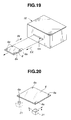
- Fig. 14 is an exploded perspective view illustrating a main part of the construction of the exposure apparatus according to the fifth embodiment of the invention.
- Figs. 15A and 15B illustrate a schematic construction of the exposure apparatus of this embodiment.
- Fig. 15A is a schematic construction view while Fig. 15B is a view illustrating part of the projection image that is obtained when having looked at the upper surface of the substrate from the arrow B indicated direction of Fig. 15a.
- the basic main construction part of the exposure apparatus 1D of this embodiment has substantially the same construction as that of the first embodiment. That main construction, as illustrated in Fig. 15A, comprises the circuit pattern storage device 7, the data-processing device 8, and exposure means 2D constructed of the illumination device 3 comprised of the illuminators 3a, 3b, 3c, ---, the image display device 4 comprised of the liquid crystal display panels 4a, 4b, 4c, ---, and the magnifying projection optical system 5 comprised of the lenses 5a, 5b, 5c, ---.
- That main construction further comprises an imaging device 12 that is image-measuring means 12 comprised of CCDs 12a, 12b, 12c, --- that get the image projected onto the exposure surface of the substrate 6 as image data and output it to the data-processing device 8, and a beam splitter 11 that is light beam splitting means comprised of a plurality of prisms 11a, 11b, 11c, --- that each guide to the imaging device 12 the beams of light that are obtained after the light beams having transmitted through the respective liquid crystal display panels 4a, 4b, and 4c of the image display device 4 have been reflected by the substrate 6.
- an imaging device 12 that is image-measuring means 12 comprised of CCDs 12a, 12b, 12c, --- that get the image projected onto the exposure surface of the substrate 6 as image data and output it to the data-processing device 8, and a beam splitter 11 that is light beam splitting means comprised of a plurality of prisms 11a, 11b, 11c, --- that each guide to the imaging device 12
- FIG. 14 there is illustrated an example of the exposure apparatus 1D that is constructed with a form wherein the liquid crystal display panels 4a, 4b, 4c, --- of the image display device 4 are disposed in a column / row fashion of vertical 3 columns and horizontal 3 rows.
- the exposure apparatus 1D of this embodiment correspondingly to the respective liquid crystal display panels 4a, 4b, 4c, ---, the same number of lenses 5a, 5b, 5c, ---, each prisms 11a, 11b, 11c, --- of the beam splitter 11, and CCDs 12a, 12b, 12c, --- are respectively provided.
- the exposure apparatus 1D of this embodiment that has been constructed in such way forms a projection image such as that illustrated, for example, in Fig. 14 or Fig. 15B with respect to the exposure surface of the substrate 6.
- the divisional region images are shown in alphabetic characters of "A”, "B”, “C”, “D”, “E”, “F” , “G”, “H” , “I”, etc. and these region images as a whole are deemed as being a circuit pattern image.
- a given unit of circuit pattern data is read out from the circuit pattern data that is stored in the circuit pattern storage device 7 by the data-processing device 8.
- the data-processing device 8 performs prescribed divisional signal processing, etc. with respect to the thus-read-out circuit pattern data and then outputs the resulting data signal to the respective liquid crystal display panels 4a, 4b, 4c, --- of the image display device 4.
- the respective divisional region images are display in their corresponding liquid crystal display panels 4a, 4b, 4c, ---.
- the respective liquid crystal display panels 4a, 4b, 4c, --- of the image display device 4 be illuminated by the illuminators 3a, 3b, 3c, ---.
- the beams of light that form the display images are transmitted through the respective prisms 11a, 11b, 11c, --- of the beam splitter 11.
- the resulting beams of light then are transmitted through the respective lenses 5a, 5b, 5c, --- of the magnifying projection optical system 5.
- the thus-magnified images are projected on the surface of exposure of the substrate 6 (refer to Figs. 14 and 15B).
- a plurality of the divisional region images that are projected onto the surface of exposure of the substrate 6 are projected in a state wherein they are arrayed in a column / row fashion.
- duplex regions In each of these duplex regions, it is necessary that adjacent ones of the divisional region images be projected in a form of their being reliably overlapped upon each other. Accordingly, in the duplex regions corresponding to the respective divisional region images, there are displayed alignment marks (in Figs. 14 and 15B they are indicated by the symbols A11, A12, A13, B12,k B13, D11, D13, E13, etc.) for performing relative positional alignments of the images.
- these alignment marks are projected onto the surface of exposure of the substrate 6 together with the respective divisional region images, and those alignment marks each consist of a prescribed image such as, for example, a mark shaped like a notation symbol "+" illustrated in Fig. 14, etc. Those alignment marks are in those states set to be the same in shape and in size.
- the beams of light that form the respective divisional region images ("A", ---, and "I") that are projected onto the surface of exposure of the substrate 6 are reflected by the surface of exposure of the substrate 6. They then enter into their respective corresponding prisms 11a, 11b, 11c, of the beam splitter 11 and are reflected by the interiors of those prisms 11a, 11b, 11c, ---. They then are guided to their respective CCDs 12a, 12b, 12c, --- of the imaging element 12 to thereby form the divisional region images corresponding to their receiving surfaces.
- the respective CCDs 12a, 12b, 12c, --- perform prescribed photo-electric conversion processing, etc. with respect to those images that have been thus optically formed. And, the resulting images are converted to image data and are output to the data-processing device 8.
- the data-processing device 8 Upon receipt of the resulting data, the data-processing device 8 performs prescribed measurement processing on the projection data and reflects the result of its calculations in an image signal that is output to the image display device 4. Namely, the data-processing device 8 performs correction processing on the display image displayed in the image display device 4, too.
- This correction processing is performed, for example, as follows.
- Fig. 16 is a view illustrating the duplex regions each of that exists between the following two images.
- One is an image that is represented by the image data that is gotten by the CCD 12a of the imaging element 12 of the exposure device 1D of this embodiment.
- the other is an image that is represented by each of the adjacent CCDs and that is adjacent to that image.
- the circuit pattern based on the use of a given unit of circuit pattern data is displayed using the image display device 4. It is thereby arranged that the magnified circuit pattern image be projected on the surface of exposure of the substrate 6.
- circuit pattern image projected onto the substrate 6 in that way be re-imaged on the receiving surface of the imaging element 12 via the beam splitter 11.
- the image that is re-imaged on the receiving surface of the CCD 12a is as illustrated in Fig. 16.
- the divisional region image 12aa (in Fig. 16 the pattern image exhibited by the character "A") of the prescribed circuit pattern.
- this divisional region image 12aa there are included the alignment marks (refer to the symbols A21, A22, and A23 illustrated in Fig. 16) as stated previously.
- the symbols B22 and B23 in Fig. 16 represent the alignment marks that are included in the divisional region image 12bb of the CCD 12b that is adjacent to the divisional region image 12aa of the CCD 12a.
- the symbols D21 and D23 represent the alignment marks that are included in the divisional region image 12dd of the CCD 12d that is adjacent to the divisional region image 12aa of the CCD 12a.
- the symbol E23 represents the alignment marks that are included in the divisional region image 12ee of the CCD 12e that is adjacent to the CCD 12a.
- the respective alignment marks are disposed within the duplex region (the region indicated by the symbol D of Fig. 16) that is defined between the adjacent divisional region images.
- the symbol E23 and the symbols A23, B23, and D23 are disposed at their prescribed positions within the duplex region at that the respective divisional region images 12aa, 12bb, 12dd, and 12ee of the CCDs 12a, 12b, 12d, and 12e are overlapped upon one another.
- the prescribed alignment marks are disposed at prescribed positions of the respective divisional region images.
- the divisional region image including therein those alignment marks are subjected to photoelectric conversion processing through the operation of the imaging element 12 and thereby converted to data and transmitted to the data-processing device 8.
- the data-processing device 8 not only performs divisional signal processing and other prescribed pieces of signal processing on the resulting data but also performs position correction processing based on the use of the image data that has been gotten by the imaging element 12, on that resulting data.
- the region data that has been prepared in this way is output to the respective liquid crystal display panels 4a, 4b, and 4c of the image display device 4.
- the region data that has thus been output thereto is projected onto the surface of exposure of the substrate 6. Accordingly, the image that is projected at this time is one that is already position correction processed so as to take a form wherein the mutually corresponding alignment marks have reliably overlapped each other within the duplex region between adjacent ones of the divisional region images.
- the above-described positional aligning operations of the respective divisional region images are performed in advance of actually performing the exposure operations with respect to the substrate 6.
- the positional aligning operation of the respective divisional region images that is performed in the exposure apparatus 1D of this embodiment is performed by converting the circuit pattern image projected on the exposure surface of the substrate 6 to image data through the operation of the imaging element 12. Accordingly, the positional aligning operation is followed by the exposure operation that is performed with respect to the substrate 6. However, at the time of this positional aligning operation, it is of course preferable to prevent the substrate 6 from being actually exposed.
- a wafer, glass plate, etc. having a photo-resist coated thereon is used as the substrate 6.
- This photo-resist in an ordinary case, has a characteristic such as that illustrated in Fig. 17 with respect to the natural logarithm.
- Fig. 17 is a view illustrating a characteristic curve of the photo-resist.
- the photo-resist has the characteristic that if the amount of exposure is within a prescribed range (the hatched portion indicated by the symbol h), the solubility thereof exhibits no decay. Accordingly, at the time of the exposure (also called "pre-exposure") that is performed beforehand for performing positional alignment, it is only needed to give an amount of exposure within a range not going beyond that prescribed amount h of exposure.
- the following effect can be obtained by providing the means for correcting relative positional alignment of the projection images that correspond to the respective divisional region images. Namely, it is possible to project the single unit of circuit pattern image, which is prepared based on the use of a desired unit of circuit pattern data, onto the prescribed substrate in a more faithful form.
- the alignment marks are included in the respective divisional region images.
- the same effect can be obtained even with use of an image recognizing technique for recognizing the configuration of the respective divisional region images, i.e., circuit pattern per se and without forming the alignment marks in particular.
- the beam splitter 11 (the light beam splitting means) and the imaging element 12 (the image measurement means) are disposed prescribed space between the image display device 4 and the substrate 6. It is thereby arranged to get the image data for positional alignment from the reflected light beam of the image that has been projected on the substrate 6.
- means, which is shown next, can also be considered as being available therefor.
- Fig. 18 is an enlarged perspective view illustrating the construction of a main part of the exposure apparatus according to a sixth embodiment of the present invention. It is to be noted that, in Fig. 18, for brevity of the illustration, the exposure apparatus and the object to be worked (substrate) with respect to that exposure is performed by this exposure apparatus are respectively illustrated by being partly broken away.
- the basic construction of the exposure apparatus lE of this embodiment is substantially the same as that of the above-described first embodiment. But as shown in Fig. 18, that construction differs from the latter construction in that at a prescribed position on a side that is opposite to that where the exposure means 2E is disposed with the substrate 6 being placed therebetween there is disposed the imaging device 21 that is the image measurement means comprised of the imaging element.
- this imaging device 21 it is set that only part of the divisional region images alone, which is taken with respect to the whole range of the circuit pattern projected onto the substrate 6, can be imaged by the imaging operation that is performed once. And, this imaging device 21 is disposed in such a way as to be freely movable in the arrow X indicated direction and arrow Y indicated direction of Fig. 18. In this imaging device 21, it is thereby arranged that the image data over the whole range of the circuit pattern image can be gotten while the device 21 is continuously performing its imaging operation while being moved.
- the other construction is the same as that of the first embodiment.
- the exposure apparatus 1E of this embodiment having the above-described construction, as in the above-described fifth embodiment, it is arranged for the pre-exposure operation to be performed in advance of the performance of the actual exposure operation.
- the single unit of circuit pattern image that is displayed by the image display device 4 is projected, by being magnified, onto the exposure surface of the substrate 6 by the magnifying projection optical system 5.
- the substrate 6 is one that consists of a glass plate or the like. Therefore, the projection image that is formed on the substrate 6 is transmitted through the substrate 6, and is imaged by the imaging device 21 that is disposed on a reverse surface side (the lower part in Fig. 18) of the substrate 6.
- the imaging device 21 it is arranged to receive the circuit pattern image (optical image) that is formed on the substrate 6 and thereby to perform photoelectric conversion with respect thereto. It is thereby arranged to output the resulting image data to the data-processing device (no illustration thereof is made in Fig. 18. See the symbol 8 in Fig. 15A) as a prescribed format of image data. And, in the data-processing device 8, various kinds of pieces of signal processing including position correction processing are performed with respect to that image data. These piece of signal processing are the same as those which are performed in the above-described fifth embodiment.
- the same advantage as is obtainable with the fifth embodiment can be obtained. Further, in this embodiment, compared to the above-described fifth embodiment, it is possible to omit the constituent members such as the beam splitter 11 serving as the light beam splitter means, etc. Therefore, it is possible to realize the same effect with a simple construction.
- the LCD that is manufactured using the exposure apparatus, etc. each are generally of a type wherein various kinds of circuit patterns are formed over a plurality of layers. Accordingly, at the time of the manufacture, the exposure operation is repeatedly performed for each layer. In this case, correcting the positional displacement of the image at the time of the next exposure operation, for example, by utilizing the circuit pattern or alignment marks that are prepared on the exposure surface of the substrate 6 in a preceding process step is possible.
- Figs. 19 and 20 are conceptual views each illustrating the exposure apparatus according to a seventh embodiment of the invention.
- Fig. 19 illustrates the exposure apparatus as a whole.
- Fig. 20 illustrates the positional relationship between the image measurement means (imaging device) of the exposure apparatus of this embodiment and the substrate with respect to that exposure is performed using that exposure apparatus.
- the basic construction of the exposure apparatus of this embodiment is the same in construction as the above-described sixth embodiment. Therefore, a detailed explanation of the respective kinds of constituent members that constitute the exposure apparatus is omitted.
- the exposure apparatus 1E of this embodiment has provided at a prescribed position of its externally covering part a substrate insertion / removal opening lm so as to enable the desired substrate 6 wanted to be manufactured to be disposed to a prescribed position of the interior thereof and taken out from this prescribed position.
- the substrate 6 is subjected to the exposure processing that is performed a plurality of times in the process of manufacturing the substrate 6. However, in this case, it sometimes happens that pieces of processing that are separate from the exposure processing, such as cleaning processing or thermal treatment, are performed. These separate pieces of processing are performed using, for example, the apparatus that is different from the exposure apparatus 1E. With this being taken into consideration, the substrate 6 that is in the course of the processing is made freely removably insertable with respect to the exposure apparatus 1E.
- the operation that is performed in that case is as follows. Namely, first, the substrate 6 is installed to within the exposure apparatus lE, thereby prescribed exposure processing is performed. Thereafter, in order to perform separate processing such as cleaning processing with respect to the substrate 6 that has already been processed until midway, the substrate 6 is taken out from the exposure apparatus 1E.
- the arrow mark EX in Fig. 19 indicates that the substrate 6 can be taken out from the exposure apparatus 1E.
- the substrate 6 is subjected to prescribed separate pieces of processing (cleaning, heating, etc.) with the use of the separate apparatus or the like (not illustrated). Thereafter, that substrate 6 is installed to a prescribed position of the interior of the exposure apparatus lE again and is subjected to the next exposure processing.
- the arrow mark IN in Fig. 19 indicates that the substrate 6 can be mounted to the exposure apparatus 1E.
- the exposure apparatus 1E of this embodiment it is arranged that, for example, when performing preceding exposure processing, the alignment marks 6a be formed at prescribed positions that are located on the exposure surface of the substrate 6. And, when performing the next exposure processing, the pre-exposure operation is performed in advance thereof. It is thereby arranged to perform positional alignment of the projection image according to those alignment marks 6a.
- the procedure of performing positional alignment in this case is performed in completely the same way as in the above-described sixth embodiment. That is, in the interior of the exposure apparatus 1E, at a position that opposes the exposure means 2 and that is on a side that is opposite to the side of the exposure means 2 with the intervention of the substrate 6 between these two sides, the imaging device 21 is sequentially moved according to a prescribed procedure in the arrow X direction and arrow Y direction of Fig. 20. While these sequential movements are being performed, the exposure apparatus 1E gets image data of the projection image (circuit pattern image) of the substrate 6. This image data is transmitted to the data-processing device 8 where various kinds of pieces of signal processing including position correction processing are performed.
- the exposure operation is performed a plurality of times. Simultaneously, even when the substrate 6 is de-mounted from and re-mounted into the exposure apparatus 1E and thereby separately processed, the exposure processing of the circuit pattern image can reliably be executed with respect to a prescribed position of the substrate 6.
- the position correction (measurement) means of this embodiment can also be easily applied to the exposure device of each of the other embodiments such as that the exposure device 1D of the above-described fifth embodiment similarly as well.
- the amount of illumination light i.e. amount of exposure light that is used when pre-exposure is performed for the positional alignment of the projection images that are projected onto the substrate 6.
- this control of the amount of exposure light it is arranged to enable forming the projection images the respective positions of that can be aligned with one another and also to cause the amount of exposure light to become equal to or smaller than a prescribed range of amount of exposure light that has no bad effect upon the normal or regular exposure.
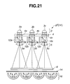
- Fig. 21 is a construction view illustrating a main part of the exposure apparatus according to an eighth embodiment of the present invention.
- the basic construction of the exposure device 1F of this embodiment is substantially the same as that of the above-described fifth embodiment (see Fig. 14). Also, in the exposure apparatus of this embodiment, it is arranged that, as in the above-described sixth embodiment (see Fig. 18), correction processing be performed for performing positional alignment according to the circuit pattern or alignment marks that were formed in the performance of the immediately preceding exposure processing.
- the exposure means 2F of the exposure apparatus 1F of this embodiment differs from the fifth embodiment in that that exposure means 2F does not use the beam splitter 11 that is the light beam splitter means of the exposure apparatus 1D of the fifth embodiment. Instead, the exposure means 2F has disposed therein a plurality of dichroic prisms 13a, 13b, and 13c each of that has an optical characteristic enabling the transmission or reflection of the light beam whose wavelength is within a specified region.
- the measuring illumination device 16 At a prescribed position on a side that is opposite to the side wherein the exposure means 2F is disposed, with the substrate 6 existing between the two sides, there is disposed the measuring illumination device 16. The light that is emitted from this measuring illumination device 16 is illuminated onto the substrate 6 via an orange-colored color filter 14.
- the dichroic prisms 13a, 13b, and 13c each are formed so as to have a characteristic of transmitting the beam of G-ray light and reflecting the beam of light whose wavelength is in the range of orange color light.
- the illumination device 3 is one for illuminating the image display device 4 when the exposure operation of the circuit pattern image is performed with respect to the substrate 6, the beam of illumination light of that illumination device 3 contains a light of G rays.
- the beam of illumination light from the measuring illumination device 16 transmits the orange-colored color filter 14, thereby the light beam of orange color components illuminates the substrate 6.
- the measuring illumination device 16 when performing the positional alignment of the projection images in advance of the actual performance of the exposure operation, first, using the measuring illumination device 16 illumination is performed of the substrate 6 from a reverse surface side (the lower side in Fig. 21) thereof. Then, because the circuit pattern that is already formed on the exposure surface of the substrate 6 through the preceding exposure processing has the color components through the function of the color filter 14, that circuit pattern is reflected by the dichroic prisms 13a, 13b, and 13c. This circuit pattern then is guided to the CCDs 12a, 12b, and 12c, thereby the circuit pattern images are formed on their respective light receiving surfaces thereof. Upon receipt thereof, the CCDs 12a, 12b, and 12c perform their respective pieces of photoelectric conversion processing, etc.
- this image data is transmitted to the data-processing device (no illustration thereof is made in Fig. 21. See the symbol 8 of Fig. 15A) where various kinds of pieces of signal processing including the position correction processing are performed with respect thereto.
- the image with respect to that position correction processing for positional alignment has been done in that way is displayed in the liquid crystal display panels 4a, 4b, and 4c of the image display device 4, thereby a state where the actual exposure operation can be performed results.
- the measuring illumination device 16 is changed over to the exposure illumination device 3, thereby the radiation of illumination light by this illumination device 3 starts to be performed.
- the illumination light beam (containing therein G-ray light) from the illumination device 3 is radiated onto the display images of the respective liquid crystal display panels 4a, 4b, and 4c of the image display device 4.
- the illumination light forming the circuit pattern image according to those display images is transmitted through the dichroic prisms 13a, 13b, and 13c and then through the respective lenses 5a, 5b, and 5c of the magnifying projection optical system 5 to reach the exposure surface of the substrate 6. That illumination light thereby projects the magnified circuit pattern image there so that this light may provide a prescribed amount of exposure for a prescribed length of time. In this way, the exposure operation is performed.
- the measuring illumination device 16 is provided separately from the exposure illumination device 3. It is thereby arranged to perform the pre-exposure processing for positional alignment by the use of the light beam that has a wavelength region different from the wavelength region at the time of the regular exposure operation and that is unable to expose the substrate 6. Therefore, the pre-exposure operation has no adverse effect upon the substrate 6. Therefore, the exposure processing that is always reliable can be performed.
- Fig. 22 is a main-part construction view illustrating a main part of the exposure apparatus of this embodiment.
- the basic construction of the exposure apparatus 1G of this embodiment is also substantially the same as that of the fifth embodiment (see Fig. 14).
- the exposure apparatus of this embodiment unlike the eighth embodiment (see Fig. 21), it is arranged, as in the case of the fifth embodiment, to perform correction processing for positional alignment according to the alignment marks projected along with the images or to the circuit pattern image per se.
- the exposure means 2G of the exposure apparatus 1G of this embodiment is characterized by having disposed therein, in addition to completely the same construction as that of the exposure device 1D of the fifth embodiment, a wavelength changeover filter 17 that is comprised of two kinds of color filters 17a and 17b each capable of transmitting a light beam whose wavelength is within a specified region.
- the wavelength changeover filter 17 is disposed so as to be freely slidable in the arrow X direction of Fig. 22.
- said other color filters 17b are so set as to be disposed at their prescribed positions that oppose their respective illuminators 3a, 3b, and 3c of the illumination device 3 and their respective liquid crystal display panels 4a, 4b, and 4c of the image display device 4.
- Fig. 22 illustrates this state.
- the illumination lights from the respective illuminators 3a, 3b, and 3c are radiated onto the display surface of the respective liquid crystal display panels 4a, 4b, and 4c by being passed through the color filters 17b only in terms of the orange color light beam. Accordingly, the projection image that is formed on the exposure surface of the substrate 6 does not make the photo-resist of the substrate 6 sensitive to that light beam.
- the projection image that has been projected onto the exposure surface of the substrate 6 is re-imaged onto the light receiving surfaces of the respective CCDs 12a, 12b, and 12c of the imaging element 12 via the beam splitter 11 comprised of the prisms 11a, 11b, and 11c.
- the respective CCDs 12a, 12b, and 12c perform prescribed photoelectric conversion processing, etc. with respect to the resulting image to thereby get image data of the projection image.
- the image data is transmitted to the data-processing device (no illustration thereof is made in Fig. 22. See the symbol 8 of Fig. 15A), whereby various kinds of pieces of signal processing including position correction processing are performed.
- the image with respect to that position correction processing for positional alignment has been performed is displayed in the liquid crystal display panels 4a, 4b, and 4c, thereby a state where the actual exposure operation can be performed results.
- the wavelength changeover filter 17 is set to a state at the time of the exposure operation. Namely, the filter 17 is set to a state where one color filters 17a have been disposed at prescribed positions that oppose their respective illuminators 3a, 3b, and 3c and their respective liquid crystal display panels 4a, 4b, and 4c. Resultantly, the illumination lights from the respective illuminators 3a, 3b, and 3c are radiated onto the display surface of the liquid crystal display panels 4a, 4b, and 4c by being passed through the color filter 17a only in terms of the G-ray light alone. Accordingly, the projection image that is formed on the exposure surface of the substrate 6 makes the photo-resist of the substrate 6 sensitive to those lights, thereby prescribed exposure is performed.
- the exposure apparatus 1G of this embodiment makes one color filter 17a have the optical characteristic of permitting the transmission of light beam whose wavelength is within a region contributing to performing the exposure operation and makes the other color filter 17b have the optical characteristic of permitting the transmission of light beam whose wavelength is within a region not contributing to performing the exposure operation.
- the pre-exposure operation has no adverse effect upon the substrate 6 and can therefore execute position correction processing according to the projection image.
- Fig. 23 is a main-part construction view illustrating a main part of the exposure apparatus of this embodiment.
- the basic construction thereof is substantially the same as that of the above-described fifth embodiment.
- the exposure means 2E is constructed using a DMD (Digital Micro-mirror Device) 18 as the display device constituting the image display means.
- DMD Digital Micro-mirror Device
- the DMD 18 is used as the display device.
- the DMD 18 has the function of displaying the image as in the case of the respective liquid crystal display panels 4a, 4b, and 4c of the image display device 4 in each of the respective embodiments. For that reason, in each DMD 18, a plurality of fine (e.g., ten-odd ⁇ m (microns) square or so of) mirror members are disposed being two-dimensionally arrayed, thereby a display surface capable of displaying, for example, a ten-odd mm (millimeters) square of image is formed. And, each of this plurality of mirror members is independently controlled so that the angle of inclination thereof with respect to the display surface and the displacement in the direction perpendicular to the array surface thereof may be individually altered utilizing, for example, the force of the static electricity.
- fine e.g., ten-odd ⁇ m (microns) square or so of
- This DMD 18 is disposed so as to oppose the side surface of each of the respective prisms 11a, 11b, and 11c of the beam splitter 11 and simultaneously so that the display surface may become substantially parallel with the optical axis of each of the respective lenses 5a, 5b, and 5c of the magnifying projection optical system 5.
- each of the respective illuminators 3a, 3b, and 3c of the illumination device 3 for illuminating the display surface of the DMD 18 is disposed at a prescribed position that enables the illumination light beam emitted from each of those illuminators 3a, 3b, and 3c to be incident upon the display surface of the DMD 18 at a prescribed angle of incidence.
- the CCDs 12a, 12b, and 12c of the imaging element 12 used to get the image data for performing position correction processing, and the optical lenses 19a, 19b, and 19c for imaging prescribed images onto the light receiving surfaces of the respective CCDs 12a, 12b, and 12c, are respectively disposed.
- Figs. 24 and 25 are views each illustrating only the DMD (image display means) and beam splitter alone, that have been taken out from among the constituent members used in the exposure apparatus of this embodiment.
- Fig. 24 illustrates a state where the DMD is not being driven and
- Fig. 25 illustrates a state where the DMD is being driven.
- the display surface of each of the respective mirror members forming the display surface of the DMD 18 is so set as to become substantially parallel with the DMD 18.
- the illumination light beam O1 of the illumination device 3 enters into the display surface of the DMD 18 at a prescribed angle of incidence and then is reflected along an optical path indicated by the symbol 02.
- This reflected light beam O2 is so set as not to enter into the beam splitter 11.
- the light beam forming the display image of the DMD 18 is guided to neither the side of the substrate 6 nor the side of the imaging element 12.
- the DMD 18 is drive-controlled by prescribed control means (not illustrated). Thereby, a given mirror member 18a of the mirror members that form the display surface of the DMD 18 is rotated so as to have a prescribed angle of inclination with respect to the display surface of the DMD 18. Then, only the reflected light beam O3 that is reflected by the mirror member 18a that has been driven, of the illumination light beams O1 emitted from the illumination device 3, is guided to the side of the beam splitter 1.
- the rotation of the mirror member can make the light “on” and “off” (the intensity modulation of the light). Further, displacing the mirror member 18a to the direction perpendicular to the surface of array thereof can modulate the phase of the light beam that is reflected.
- the light beam O3 is guided as the light beam O5 to the side of the substrate 6 through the function of the beam splitter 11. Also, the light beam O5 that has been reflected by the substrate 6 is transmitted through the beam splitter 11 to enter into the imaging element 12 as the light beam O4. Resultantly, at the corresponding position of the light receiving surface of the imaging element 12, and at the corresponding position of the exposure surface of the substrate 6, to the light beam, a prescribed image, i.e., the display image at the mirror member 18a of the DMD 18, is projected.
- the reflected light beam O2 that is reflected by other mirror members than the mirror member 18a is in a state of being kept out of entry into the beam splitter 11 as in the non-driven state of the DMD 18 as illustrated in Fig. 25. Accordingly, with respect to the corresponding regions at the light-receiving surface of the imaging element 12 and at the exposure surface of the substrate 6, no image whatsoever is kept projected.
- the circuit pattern image to be projected is represented by the distribution of the light intensity.
- the phase information is completely lost. Therefore, calculating the amplitude information and phase information of the Fourier transform processed image that is to be displayed by the DMD (display device) 18 for projecting the desired image onto the exposure surface of the substrate 6 (the object to be worked) according to the image data of the projected circuit pattern image is followed by the performance of a very large amount of very complex operation processing.
- the amplitude information and phase information of the Fourier transform processed image that is to be displayed by the DMD 18 are calculated through the operation of the means that is shown as follows.
- the DMD 18 is used as the image display means, more easily, the desired display image can be arbitrarily projected with respect to the light-receiving surface of the imaging element 12 and to the exposure surface of the substrate 6. Accordingly, the image data for performing position correction processing of the image can be obtained with a higher accuracy and with a higher reliability.
- the circuit pattern image that is highly accurate and high in resolution can be easily projected onto the exposure surface of the substrate (the object to be worked) 6.
- Fig. 26 is a main-part construction view illustrating a main part of the exposure apparatus of this embodiment.
- the construction of this embodiment is basically substantially the same as that of the above-described tenth embodiment. But this embodiment differs from the latter embodiment in that, in the exposure apparatus 1J of this embodiment, it is constructed to distribute out the light beam directed to the image display means (DMD) and to the light beam to the side of the imaging element (CCD) through the utilization of the polarization of light.
- DMD image display means
- CCD imaging element
- the exposure apparatus 1J of this embodiment comprises a plurality of the illuminators 3a, 3b, and 3c constituting the illumination device 3, reflection mirrors 23a, 23b, and 23c that reflect the respective illumination lights from the illuminators 3a, 3b, and 3c and that guide these reflected light beams to a prescribed direction, polarizing plates 22a, 22b, and 22c that are respectively disposed in the spaces between the illuminators 3a, 3b, and 3c and their corresponding reflection mirrors 23a, 23b, and 23c to thereby make their prescribed polarization, polarized-beam splitters 24a, 24b, and 24c that are located on the optical path of the light beams reflected by the reflection mirrors 23a, 23b, and 23c and that thereby are light beam splitter means upon that those light beams enter, first ⁇ /4 plates ( ⁇ (lambda) the fourth plate) 25a, 25b, and 25c and second ⁇ /4 plates ( ⁇ (lambda) the fourth plate
- the reflection mirrors 23a, 23b, and 23c are located in the vicinity of the polarized beam splitters 24a, 24b, and 24c. And they are disposed being inclined substantially at a 45 degrees angle with respect to the optical path of the illumination light beam from the illumination device 3. And, in addition, the reflection surfaces thereof are set so as to face the illumination device 3 and the polarized beam splitters 24a, 24b, and 24c. Thereby, the illumination light beams from the illumination device 3 are reflected and are guided to the polarized light beam splitters 24a, 24b, and 24c.
- the polarized beam splitters 24a, 24b, and 24c are each so constructed as to have a characteristic of their being capable of reflecting a prescribed polarized light. And, the polarizing plates 22a, 22b, and 22c are each so set as to produce a polarized light that has a characteristic of its being capable of being reflected by the reflection surface that is provided within the polarized beam splitter 24a, 24b, or 24c.
- the illumination light beam that is radiated from the illumination device 3 goes along the optical path indicated by the arrow mark O in Fig. 26 to reach the light-receiving surface of the imaging element 12 as well as to reach the exposure surface of the substrate 6.
- the illumination light beam that is radiated from the illumination device 3 first is transmitted through the polarizing plates 22a, 22b, and 22c, thereby polarized light is formed. Thereafter, the polarized light is reflected by a corresponding one of the reflection mirrors 23a, 23b, and 23c and is guided to the side of the polarized beam splitter 24a, 24b, and 24c.
- the polarized light that has entered upon the polarized beam splitter 24a, 24b, 24c is reflected by the reflection surface within the polarized beam splitter 24a, 24b, 24c. Thereby, the polarized light is guided to the side of the DMD 18 that is located upper in Fig. 26. Then, the resulting light beam is transmitted through the first ⁇ /4 plate 25a, 25b, 25c, and then radiates the display surface of the DMD 18 and is reflected by this display surface. Then, the resulting light beam goes downward in Fig. 26 and then is transmitted through the first ⁇ /4 plate 25a, 25b, 25c once again and then is guided to the polarized beam splitter 24a, 24b, 24c.
- the vibration direction of the vibration vector is rotated through a 90 degrees angle. Accordingly, that polarized light is transmitted through the polarized beam splitter 24a, 24b, 24c.
- the light beam that has been transmitted through the polarized beam splitter 24a, 24b, 24c advances toward the side of the substrate 6 via the second ⁇ /4 plate 26a, 26b, 26c and magnifying projection optical system. As a result of this, on the exposure surface of the substrate 6 there is projected the magnified prescribed circuit pattern image. In this state, the exposure operation can be done.
- the light beam that has been reflected by the substrate 6 advances upward in Fig. 26 and is once again transmitted through the second ⁇ /4 plate 26a, 26b, 26c and then enters upon the polarized beam splitter 24a, 24b, 24c.
- the vibration direction of the vibration vector is rotated through an angle of 90 degrees again. Accordingly, the light beam is reflected by the reflection surface within the polarized beam splitter 24a, 24b, 24c.
- the light beam that has been reflected by the reflection surface of the polarized beam splitter 24a, 24b, 24c is guided to the CCD 12a, 12b, 12c, and is imaged on the light-receiving surface as a prescribed image. And, position correction processing is performed of the images according to the prescribed image data that is gotten by their corresponding respective CCDs 12a, 12b, and 12c. These pieces of position correction processing are performed substantially in the same way as in the case of the above-described fifth embodiment.
- Figs. 27 and 28 illustrate a main part of the exposure apparatus of this embodiment.
- Fig. 27 is a perspective view illustrating a main part of the exposure apparatus while
- Fig. 28 is a construction view that is taken when the exposure apparatus is viewed from its side surface.
- the construction of this embodiment is basically substantially the same as that of the above-described fifth embodiment (see Fig. 14 and Figs. 15A and 15B).
- the respective CCDs 12a, 12b, and 12c constituting the imaging element 12 are disposed in the vicinities of their respective corresponding light beam splitter means (the prisms 11a, 11b, and 11c of the beam splitter 11, in the exposure apparatus 1K of this embodiment a plurality of the CCDs 12a, 12b, 12c, 12d, 12e, 12f, 12g, and 12h constituting the imaging element 12 are collectively disposed at the same prescribed position within the exposure apparatus 1K.
- an electric circuit for controlling the respective CCDs 12a, 12b, 12c, 12d, 12e, 12f, 12g, and 12h, wiring therefor, etc. also are disposed at their prescribed positions.
- a plurality of semi-transmission mirrors (half mirrors) 20 are provided so as to correspond to the respective CCDs 12a, 12b, and 12c.
- the remaining construction is the same as that of the above-described fifth embodiment.
- the illumination device and the image display device are not illustrated.
- the image display device 4 is disposed in the space between the illumination device 3 and half mirrors 20 provided at the upper prescribed positions.
- the same effect as attainable with the fifth above-described embodiment can be obtained.
- various kinds of members constituting the exposure apparatus 1K can be efficiently disposed. So this can contribute to miniaturizing the exposure apparatus 1K per se including the exposure means 2K.
- Fig. 29 is a main-part construction view illustrating a main part of the exposure apparatus according to a thirteenth embodiment of the present invention.
- the basic construction of the exposure apparatus 1L of this embodiment is substantially the same as that of the above-described fifth embodiment (see Fig. 14).
- the projection unit 31 including the magnifying projection optical system 5 and image measurement means is two-dimensionally moved within a flat plane that opposes the substrate 6 that becomes an object to be worked by the use of prescribed moving means. It is thereby arranged to project a desired circuit pattern image onto the exposure surface of the substrate 6.
- the exposure apparatus 2L of this embodiment it is set that the range over that the exposure operation, which is performed once, can expose the substrate 6 becomes part of the whole region with respect to that exposure is to be performed. And, while moving the projection unit 31 within the prescribed two-dimensional flat plane in the arrow X and arrow Y directions of Fig. 29, the exposure operation is performed a plurality of times. It is thereby arranged to perform exposure of a single unit of circuit pattern image with respect to the whole of a prescribed region of the substrate 6.
- the projection unit 31 is constructed of a plurality of the magnifying projection optical systems 5, a plurality of the imaging elements 12, a plurality of the half mirrors 20 or a plurality of the beam splitters 11. Because the basic construction of the projection unit 31 is substantially the same as in the case of the above-described fifth embodiment or twelfth embodiment or other, a detailed explanation thereof and an illustration of the concrete construction are omitted.
- the image display device 4 constituting the exposure means 2L, the illumination device (not illustrated) provided at a prescribed position that is located upper than the device 4, and the substrate 6 that is an object to be worked with respect to that exposure is performed, are each in a state of being made fixed.
- the projection unit 31 is located in the space between the image display device 4 and the substrate 6.
- the projection unit 31 is constructed so as to be two-dimensionally moved within a prescribed flat plane that opposes the substrate 6 by a moving mechanism (not illustrated) that is prescribed moving means that is formed using a motor, etc.
- the image display device 4 has provided therein a plurality of the liquid crystal display panels 4a, 4b, 4c, ---, 4n so as for them to cover the whole of a prescribed range of the substrate 6 with respect to that exposure is to be performed. It is thereby arranged that the single unit of circuit pattern image that is to be exposed be displayed thereon at all times.
- Fig. 30 is a schematic construction view schematically illustrating the construction of the exposure apparatus according to the fourteenth embodiment of the invention.
- Fig. 31 is a schematic construction view schematically illustrating the construction of a pattern exposure unit in the exposure apparatus of this embodiment.
- the exposure apparatus of this embodiment is for manufacturing a high-density printed substrate such as a BGA substrate or CSP substrate, which has printed thereon a desired circuit pattern, without using an exposure printing mask.
- This exposure apparatus has a construction wherein the circuit pattern standing on the use of prescribed data representing a desired circuit pattern is displayed by the display means such as liquid crystal display panels. This display is projected onto the exposure surface of a prescribed substrate material member. Thereby, exposure is performed with respect thereto.
- the exposure apparatus 1 of this embodiment is constructed so as to receive circuit pattern data, such as substrate design data, prepared by the circuit pattern being converted to a prescribed format of data and to perform prescribed signal processing thereon.
- the exposure apparatus 1 comprises a controller 2 that is control means for performing general control over the whole exposure apparatus 1, a plurality of pattern exposure units 3 that performs exposure of the whole of a desired circuit pattern onto a prescribed position of the exposure surface of the prescribed substrate material member 10 becoming the object to be manufactured every prescribed-region circuit pattern, and a plurality of horizontal position-adjusting mechanisms 4 for adjusting the positions in the horizontal direction of a plurality of the pattern exposure units 3, i.e., the positions thereof within a plane parallel with the exposure surface of the substrate material member 10 to be exposed.
- the controller 2 comprises an interface part (the part indicated simply as "I/F" in Fig. 30) 2a that is connection means for receiving data transmitted from an external device (not illustrated) having recorded therein in a prescribed format the desired substrate design data, etc., a substrate disposition code generator 2b that generates code signals for disposing respective ones of a plurality of the pattern exposure units 3 upon receipt of prescribed data signals from that interface part 2a so that those respective pattern exposure units may be situated at their prescribed positions relative to the exposure surface, a circuit pattern code generator 2c that generates code signals representing the circuit pattern regions corresponding to the individual pattern exposure units 3 upon receipt of the data signals from the interface part 2a, and a pattern code correction circuit 2d that performs prescribed pieces of correction processing with respect to the code signals representing the circuit pattern regions generated from the circuit pattern code generator 2c, e.g. signal correction processing for correcting the distortions that optically occur in those code signals, etc.
- the pattern exposure unit 3 is constructed of a plurality of pattern exposure units each having the same construction such as, for example, a first pattern exposure unit 3a, second pattern exposure unit 3b, ---, nth pattern exposure unit 3n.
- the individual pattern exposure units 3 are disposed in Fig. 30 in one row in the lateral direction, they may be arranged, for example, in a column / row fashion (in the form of a matrix).
- the horizontal position-adjusting mechanism 4 is constructed so that a plurality of horizontal position-adjusting mechanisms each having the same construction, such as a first horizontal position-adjusting mechanism 4a, second horizontal position-adjusting mechanism 4b, ---, nth horizontal position-adjusting mechanism 4n, may correspond to the respective ones of the above-described pattern exposure units 3.
- These horizontal position-adjusting mechanisms 4 are ones for adjusting the positions of the individual pattern exposure units 3 correspondingly to the kinds of the printed substrate to be manufactured. The position adjustment therefor is performed according to the input substrate design data. A detailed construction of the pattern exposure unit 3 in the exposure apparatus 1 of this embodiment will hereafter be explained.
- the pattern exposure unit 3 of this exposure apparatus 1, as illustrated in Fig. 31, comprises the liquid crystal display device (hereinafter referred to simply as "LCD") that is display means for displaying as the image the circuit pattern that is represented by the circuit pattern code data (signal) transmitted on from the controller 2, and that is comprised of a liquid crystal display panel, etc., an LCD driver 7 that performs drive control of the LCD 6, a light source 5 that illuminates the display made by the LCD 6, a projection optical system 8 that is comprised of a plurality of optical lenses, etc.
- LCD liquid crystal display device
- a magnification adjustment mechanism 9 for adjusting the magnification by moving that projection optical system 8 in the direction that is along the optical axis thereof.
- the LCD 6 is used as the means for displaying as the image the circuit pattern represented by the substrate design data, i.e. the means for modulating the spatial intensity distribution of the illumination light from the light source 5 according to the circuit pattern (circuit pattern code data) represented by the substrate design data.
- the embodiment is not limited to this way of use of the LCD 6.
- a DMD digital micro-mirror device
- This DMD is one that has a function of modulating the spatial intensity distribution of the illumination light by controlling the direction of the reflected light beam.
- the high-density printed substrate that is to be manufactured by the exposure apparatus 1 of this embodiment, there are, for example, a BGA substrate, CSP substrate, etc.
- a BGA substrate for example, a BGA substrate, CSP substrate, etc.
- CSP substrate for example, a BGA substrate, CSP substrate, etc.
- Fig. 32 is a conceptual view illustrating the BGA substrate
- Fig. 33 is a conceptual view illustrating the CSP substrate.
- illustration is simultaneously made of the range of the exposure region with respect to that exposure can be performed with a single piece of the pattern exposure unit of the exposure apparatus.
- the BGA substrate, CSP substrate, etc. each are formed as illustrated in Figs. 32 and 33.
- one substrate frame (also simply called “a frame") 21, 31 is formed of a plurality of circuit patterns (also called “pieces") 22, 32.
- circuit patterns also called "pieces" 22.
- three pieces 22 constitute one frame 21.
- the high-density substrate such as the BGA substrate 20 or CSP substrate 30, ordinarily, is formed in such a way that a plurality of the same circuit patterns (pieces) 22, 32 are arrayed within one substrate frame 21, 31.
- the exposure region with respect to that exposure can be performed by the pattern exposure unit 3 at one time is set so as to fall upon the region (the symbols 23, 33) surrounded by a dotted line in Fig. 32, 33.
- the individual pieces 22 that form this substrate 20 each is formed of a relatively large-sized pattern.
- the exposure apparatus 1 as illustrated in Fig. 32, it is set that with respect to the BGA substrate one piece 22 can be exposed by one pattern exposure unit 3 at one time. Accordingly, in the example of the BGA substrate 20 illustrated in Fig. 32, using the three pattern exposure units 3, the circuit pattern of the whole BGA substrate 20 can be exposed through the performance of one exposure operation.
- the pattern size of the individual pieces 32 forming the substrate 30 is set to a relatively small pattern size.
- the size of one piece of the BGA substrate 20 illustrated in Fig. 32 correspond to the size of four pieces of the CSP substrate 30 illustrated in Fig. 33.
- the CSP substrate 30 it can be set that, with respect to the mutually adjacent four pieces 32, exposure can be performed by one pattern exposure unit 3 at one time.
- the circuit pattern of the whole CSP substrate 30 can be exposed through the performance of one exposure operation.
- the amount of the exposure regions that is exposed by one pattern exposure unit 3 at one time is set in units of a piece. Namely, it is set that, within the exposure region that is exposed by one pattern exposure unit 3, one, or a plurality of, pieces 22, 32 are included in units of a piece. And, it is set that, with one piece 22, 32 being divided into smaller sized pieces, the respective regions of the thus-divided pieces are prevented from being set so as to be exposed by their respective different pattern exposure units 3.
- substrate design data is input to the substrate disposition code generator 2b and to the circuit pattern code generator 2c via the interface part 2a.
- the substrate disposition code generator 2b According to the substrate design data signals input thereto there are generated prescribed code signals for setting the first to nth pattern exposure units 3a to 3n so as for respective ones of these units 3a to 3n to be disposed at their corresponding prescribed positions that oppose the exposure surface of the substrate material member 10.
- the code signals that have been generated from there are transmitted to the first to nth horizontal position-adjusting mechanisms 4a to 4n, thereby performing drive control of their corresponding first to nth pattern exposure units 3a to 3n in the horizontal direction, i.e., in the arrow Y direction of Fig. 30 to thereby adjust these exposure units to their respective prescribed positions.
- the circuit pattern code generator 2c according to the substrate design data signal input thereto, there are generated code signals of the prescribed circuit patterns. And, the code signals of the circuit patterns that have been generated from there are output to the first to nth pattern exposure units 3a to 3n, respectively.
- correction data is one that is used in the following case.
- the exposure apparatus 1 is constructed so that the circuit pattern image that is projected by the projection optical system 8 may be exposed to the surface of exposure of the prescribed substrate material member 10 as stated previously. Accordingly, when performing the exposure operation, a case where depending upon the projection conditions under that the projection optical system 8 performs its projection optical distortions, etc. occur in the circuit pattern image imaged on the exposure surface of the substrate material member 10 is also considered to arise. In such a case, if performing prescribed correction processing with respect to the substrate design data in advance, it becomes possible to expose the circuit pattern image that at all times accords with the substrate design data regardless of the projection conditions at the time of the exposure.
- the code correction circuit 2d comprised of an EEPROM having stored therein beforehand prescribed correction data, etc. And, from this code correction circuit 2d, correction data is read out according to the necessity. It is thereby arranged to perform signal correction processing, etc. of the code signal representing the circuit pattern that is to be generated from the circuit pattern code generator 2c.
- the signals (data) that represent the circuit pattern code and that have been thus generated from the circuit 2c are respectively output to the first to nth pattern exposure units 3a to 3n.
- the data of the circuit pattern code that is input thereto is transmitted to the LCD driver 7 and to the magnification adjustment mechanism 9 (see Fig. 31).
- the LCD driver 7 performs prescribed signal processing with respect to the circuit pattern code data that is input thereto and generates a signal having a format of its being able to be displayed as the image. And, the signal that has been generated therefrom is transmitted to the LCD 6. Upon receipt of the resulting signal, in the display part (not illustrated) of the LCD 6, a desired circuit pattern is displayed. It is to be noted that the circuit pattern that is displayed in the display part of the LCD 6 in each of the respective pattern exposure units 3a to 3n represents a partial region of the whole circuit pattern that is represented by the substrate design data. Namely, that circuit pattern is one that corresponds to the prescribed region indicated in each of Figs. 32 and 33.
- each LCD 6 is illuminated by the illumination light emitted from the light source 5 corresponding thereto.
- the circuit pattern that is being displayed in the display part of the LCD 6 is projected to a prescribed position of the exposure surface of the substrate material member 10 via the projection optical system 8. Thereby, the circuit pattern image is imaged thereon.
- control is performed so that the circuit pattern image that is to be imaged on the exposure surface of the substrate material member 10 may be imaged in a prescribed form.
- This control is performed by performing drive control of the projection optical system 8 in the arrow X direction of Fig. 31 according to a prescribed instruction signal contained in the circuit pattern code data from the controller 2.
- the fourteenth embodiment correspondingly to a plurality of the pattern exposure units 3, the same number of horizontal position adjustment mechanisms 4 are disposed. It is thereby arranged that these horizontal position adjustment mechanisms 4 adjust the positions of the individual pattern exposure units 3 according to the substrate design data that is input thereto. Accordingly, it is possible to easily cope with various kinds of circuit patterns, etc. and in hence to realize the exposure apparatus that has a simple construction and that has a high level of applicability.
- this fourteenth embodiment there is made up a construction wherein without using the exposure printing mask a desired circuit pattern is displayed in the liquid crystal display device (LCD) 6. And, that displayed circuit pattern is formed on the exposure surface of the substrate material member 10 using the projection optical system 8.
- LCD liquid crystal display device
- this exposure apparatus has equipped therein a plurality of the pattern exposure units 3, each of which is arranged to expose only a prescribed region alone of the whole circuit pattern that is to be exposed onto the whole of the substrate material member 10.
- the exposure operation that is performed by each of a plurality of the pattern exposure units 3 is simultaneously performed in parallel. Therefore, the pieces of high-speed processing can be realized with a simple construction. This also can easily contribute to reducing the manufacturing cost.
- the individual circuit pattern images that are formed on the exposure surface of the substrate material member 10 by a plurality of the pattern exposure units 3 are arranged so that those pattern images as a whole represent one unit of circuit pattern.
- the whole circuit pattern is so arranged as to be formed by a plurality of the pattern exposure units 3. Therefore, when the number of the individual circuit patterns increases, it is considered as being possible that displacements inconveniently occur in the relative positional relationship between fellow ones of the circuit pattern images formed by the individual pattern exposure units 3. In case positional displacements have occurred between fellow ones of the individual circuit pattern images, the substrate design data that correspond to the whole circuit pattern cannot faithfully be reproduced with respect thereto. Therefore, the substrate design data becomes inaccurately reproduced.
- Fig. 34 is a schematic construction view schematically illustrating the construction of the exposure apparatus according to the fifteenth embodiment of the present invention.
- Fig. 35 is a schematic construction view schematically illustrating the construction of the pattern exposure unit in the exposure apparatus of this embodiment.
- the basic construction of the exposure apparatus 1A of this embodiment is substantially the same as that of the exposure apparatus 1 of the above-described fourteenth embodiment.
- this exposure apparatus 1A as illustrated in Fig. 35, there is newly disposed additionally to the fourteenth embodiment the imaging means 11 that is provided within the pattern exposure unit 3A and that gets image data for producing correction data for correcting the positional displacement thereof with respect to the substrate material member 10.
- constituent members such as, for example, a disposition code correction circuit 2e that is provided within the controller 2A (control means) for performing general control over the exposure apparatus 1 and that produces disposition codes for correcting and setting the disposition with respect to the substrate material member 10 of the pattern exposure unit 3 according to the image data having been gotten by the imaging means 11.
- the imaging means 11 is comprised of a CCD camera 11a that has an imaging element such as a CCD, an imaging optical system 11b that condenses the light beam from the exposure surface of the substrate material member 10 and forms a prescribed image so as to image this prescribed image onto a prescribed position within the CCD camera 11a, etc.
- the image data (image signal) that is obtained through the imaging operation of the imaging means 11 is data representing the alignment marks that are provided at prescribed positions of the prescribed exposure regions (see Figs. 32 and 33) of the substrate material member 10 corresponding to the respective pattern exposure units 3, for example, the images including prescribed openings, etc. that are formed in the substrate material member 10 beforehand. It is to be noted that, in the following explanation, this image data (image signal) is referred to as "the alignment mark image signal".
- the imaging means 11 that is provided within each of the respective pattern exposure units 3 is electrically connected to the disposition code correction circuit 2e that is provided within the controller 2A. It is thereby arranged that the alignment mark image signal that is gotten by the imaging means 11 be transmitted to the disposition code correction circuit 2e.
- the disposition code correction circuit 2e is electrically connected to a substrate disposition code generator 2b within the controller 2A. It is also so arranged as to be able to receive the alignment mark image signal from the imaging means 11 of the respective pattern exposure unit 3 as stated above.
- a pattern code correction circuit 2d that is provided within the controller 2A corresponds to the code correction circuit 2d in the above-described fourteenth embodiment.
- the remaining construction is the same as in the case of the fourteenth embodiment.
- the controller 2A controls the respective imaging means 11 of the pattern exposure units 3 to thereby cause them to perform their prescribed imaging operations.
- the imaging means 11 thereby gets the corresponding alignment mark image signals.
- the respective alignment mark image signal that has been gotten by the imaging means 11 is transmitted to the disposition code correction circuit 2e of the controller 2A.
- the disposition code correction circuit 2e Upon receipt of it, the disposition code correction circuit 2e performs prescribed signal processing on it according to the thus-gotten alignment mark image signal.
- the disposition code correction circuit 2e thereafter outputs the resulting signal to the substrate disposition code generator 2b.
- the substrate design data that is input from a prescribed external device (not illustrated) to the controller 2 is input to the substrate disposition code generator 2b and to the circuit pattern code generator 2c via the interface part 2a.
- the substrate disposition code generator 2b produces, according to both of the input substrate design data signal and the above-described disposition code correction circuit 2e, a prescribed code signal for setting so that the respective pattern exposure units 3 may be disposed at prescribed positions that oppose the exposure surface of the substrate material member 10.
- the code signal that has been generated from there is transmitted to each of the respective horizontal position-adjusting mechanisms 4. Thereby, the corresponding pattern exposure units 3 are drive controlled in the horizontal direction, i.e. the arrow Y direction of Fig. 34 and are thereby adjusted so as to be located at their respective positions.
- circuit pattern code generator 2c according to the substrate design data that has been input thereto, completely the same operation as in the circuit pattern code generator 2c in the fourteenth embodiment is performed. Then, the prescribed circuit pattern signal that has been produced there is output to the respective pattern exposure units 3. In the respective pattern exposure units 3, upon receipt of that circuit pattern signal, completely the same operation as in the fourteenth embodiment is performed, with the result that a desired circuit pattern image is projected onto the exposure surface of the substrate material member 10.
- the disposition code correction circuit 2e performs prescribed pieces of correction processing to thereby produce prescribed disposition codes. And, it is thereby arranged that the respective pattern exposure units 3 are reliably disposed at their prescribed positions according to those prescribed dispositions codes. Accordingly, the exposure operation can be performed with a high level of precision. Resultantly, a higher quality of high-density printed substrate can be easily manufactured.
Applications Claiming Priority (4)
| Application Number | Priority Date | Filing Date | Title |
|---|---|---|---|
| JP34675399 | 1999-12-06 | ||
| JP34675399A JP2001168003A (ja) | 1999-12-06 | 1999-12-06 | 露光装置 |
| JP35476299 | 1999-12-14 | ||
| JP35476299A JP2001175002A (ja) | 1999-12-14 | 1999-12-14 | 露光装置 |
Publications (2)
| Publication Number | Publication Date |
|---|---|
| EP1107064A2 true EP1107064A2 (de) | 2001-06-13 |
| EP1107064A3 EP1107064A3 (de) | 2004-12-29 |
Family
ID=26578338
Family Applications (1)
| Application Number | Title | Priority Date | Filing Date |
|---|---|---|---|
| EP00125392A Withdrawn EP1107064A3 (de) | 1999-12-06 | 2000-12-04 | Belichtungsapparat |
Country Status (2)
| Country | Link |
|---|---|
| US (1) | US6515734B1 (de) |
| EP (1) | EP1107064A3 (de) |
Cited By (12)
| Publication number | Priority date | Publication date | Assignee | Title |
|---|---|---|---|---|
| EP1372036A1 (de) * | 2002-06-12 | 2003-12-17 | ASML Netherlands B.V. | Lithographischer Apparat und Verfahren zur Herstellung einer Vorrichtung |
| DE10230320A1 (de) * | 2002-07-05 | 2004-02-05 | Marcel Rogalla | Programmierbare Beleuchtungsvorrichtung zur hochauflösenden, massiv parallelen, räumlichen Systhese und Analyse von Microarrays |
| EP1422939A2 (de) * | 2002-11-25 | 2004-05-26 | Stefan Schrodt | Mehrkanaliges Projektionssystem und Verfahren zur Erzielung grosser Projektionsflächen |
| EP1491966A1 (de) * | 2003-06-26 | 2004-12-29 | ASML Netherlands B.V. | Eichverfahren für einen lithographischen Apparat |
| EP1493054A1 (de) * | 2002-04-09 | 2005-01-05 | Dicon A/S | Lichtmodulations-engine |
| EP1659452A1 (de) * | 2004-11-22 | 2006-05-24 | ASML Netherlands B.V. | Latente Überlagerungsmetrologie |
| CN1312618C (zh) * | 2003-06-20 | 2007-04-25 | 佳能株式会社 | 图像显示方法及图像显示装置 |
| US7239393B2 (en) | 2003-06-26 | 2007-07-03 | Asml Netherlands B.V. | Calibration method for a lithographic apparatus and device manufacturing method |
| WO2008081963A1 (en) * | 2007-01-04 | 2008-07-10 | Nikon Corporation | Projection optical apparatus, exposure method and apparatus, photomask, and device and photomask manufacturing method |
| WO2009078489A1 (en) * | 2007-12-17 | 2009-06-25 | Nikon Corporation | Exposure apparatus, exposure method and device manufacturing method |
| CN101976018B (zh) * | 2006-02-16 | 2013-01-30 | 株式会社尼康 | 光罩及其制造方法 |
| CN107145043A (zh) * | 2017-07-11 | 2017-09-08 | 上海镭慎光电科技有限公司 | 硅片对准标记的曝光装置和曝光方法 |
Families Citing this family (26)
| Publication number | Priority date | Publication date | Assignee | Title |
|---|---|---|---|---|
| USRE43841E1 (en) * | 2000-12-14 | 2012-12-04 | F. Poszat Hu, Llc | Printing by active tiling |
| GB0114862D0 (en) | 2001-06-19 | 2001-08-08 | Secr Defence | Image replication system |
| TW556043B (en) * | 2001-11-30 | 2003-10-01 | Asml Netherlands Bv | Imaging apparatus, device manufacturing method and device manufactured by said method |
| WO2004074934A1 (ja) * | 2003-01-28 | 2004-09-02 | Ball Semiconductor Inc. | マスク作成方法、マスク作成装置、及び、マスク描画装置 |
| EP1482373A1 (de) | 2003-05-30 | 2004-12-01 | ASML Netherlands B.V. | Lithographischer Apparat und Verfahren zur Herstellung eines Artikels |
| JP4400200B2 (ja) * | 2003-12-10 | 2010-01-20 | セイコーエプソン株式会社 | 画像表示方法、画像表示装置および画像表示プログラム |
| JP2006108212A (ja) * | 2004-10-01 | 2006-04-20 | Canon Inc | 露光装置 |
| US8149218B2 (en) | 2004-12-21 | 2012-04-03 | Universal Electronics, Inc. | Controlling device with selectively illuminated user interfaces |
| JP4984810B2 (ja) * | 2006-02-16 | 2012-07-25 | 株式会社ニコン | 露光方法、露光装置及びフォトマスク |
| JP5727140B2 (ja) * | 2006-12-18 | 2015-06-03 | トムソン ライセンシングThomson Licensing | 交互の光偏光のための回転半透明シリンダーを有する二次元/三次元プロジェクター |
| JP2010513981A (ja) * | 2006-12-18 | 2010-04-30 | トムソン ライセンシング | 色域画像映写機及び色域画像映写法 |
| US20100014008A1 (en) * | 2006-12-19 | 2010-01-21 | Youngshik Yoon | Wide color gaut high resolution dmd projection system |
| WO2008076114A1 (en) * | 2006-12-19 | 2008-06-26 | Thomson Licensing | High resolution dmd projection system |
| WO2008095227A1 (en) * | 2007-02-08 | 2008-08-14 | Silverbrook Research Pty Ltd | System for controlling movement of a cursor on a display device |
| JP2008220479A (ja) * | 2007-03-09 | 2008-09-25 | Fujifilm Corp | 放射線画像撮影装置及びその処理方法 |
| EP2156245A4 (de) | 2007-04-25 | 2011-08-31 | Thomson Licensing | Hochauflösendes 3d-projektionssystem |
| WO2009002369A1 (en) * | 2007-06-25 | 2008-12-31 | Thomson Licensing | Video recording prevention system |
| US8363209B2 (en) * | 2007-07-10 | 2013-01-29 | Lg Electronics Inc. | Method and apparatus to adjust misalignment of the maskless exposure apparatus |
| NL2003204A1 (nl) * | 2008-08-14 | 2010-02-16 | Asml Netherlands Bv | Lithographic apparatus and method. |
| JP2014027260A (ja) * | 2012-06-19 | 2014-02-06 | Canon Inc | 描画装置、データ処理方法および物品の製造方法 |
| JP6083185B2 (ja) | 2012-10-12 | 2017-02-22 | セイコーエプソン株式会社 | プロジェクター、プロジェクターの黒レベル領域設定方法 |
| EP2876498B1 (de) | 2013-11-22 | 2017-05-24 | Carl Zeiss SMT GmbH | Beleuchtungssystem eines mikrolithografischen Projektionsbelichtungsgerätes |
| KR102419494B1 (ko) * | 2014-09-29 | 2022-07-12 | 삼성디스플레이 주식회사 | 마스크리스 노광 장치, 마스크리스 노광 방법 및 이에 의해 제조되는 표시 기판 |
| WO2017040066A1 (en) * | 2015-08-31 | 2017-03-09 | The Arizona Board Of Regents On Behalf Of The University Of Arizona | Range-finder apparatus, methods, and applications |
| CN113031404B (zh) * | 2021-03-23 | 2023-08-15 | 合肥芯碁微电子装备股份有限公司 | 量产型激光直写光刻机及其控制方法 |
| US20230043353A1 (en) * | 2021-08-04 | 2023-02-09 | Onto Innovation, Inc. | Multiple camera apparatus for photolithographic processing |
Citations (5)
| Publication number | Priority date | Publication date | Assignee | Title |
|---|---|---|---|---|
| JPH06204112A (ja) * | 1992-12-30 | 1994-07-22 | Sony Corp | 露光方法及び露光装置 |
| JPH09139340A (ja) * | 1995-11-13 | 1997-05-27 | Nikon Corp | 位置ずれ補正方法 |
| US5691541A (en) * | 1996-05-14 | 1997-11-25 | The Regents Of The University Of California | Maskless, reticle-free, lithography |
| WO1998004950A1 (en) * | 1996-07-25 | 1998-02-05 | Anvik Corporation | Seamless, maskless lithography system using spatial light modulator |
| EP0926556A2 (de) * | 1997-12-20 | 1999-06-30 | Carl Zeiss | Projektionsbelichtungsanlage und Belichtungsverfahren |
Family Cites Families (20)
| Publication number | Priority date | Publication date | Assignee | Title |
|---|---|---|---|---|
| US2622071A (en) | 1951-04-09 | 1952-12-16 | Gen Mills Inc | Esterification process |
| NL299869A (de) | 1963-10-29 | |||
| US4738801A (en) | 1978-03-23 | 1988-04-19 | Nisshin Flour Milling Co., Ltd. | Antiulcer compounds |
| US4483871A (en) | 1978-03-23 | 1984-11-20 | Nisshin Flour Milling Co., Ltd. | Antiulcer compounds |
| US4642314A (en) | 1978-03-23 | 1987-02-10 | Nisshin Flour Milling Co., Ltd. | Antiulcer compounds |
| JPS5670097A (en) | 1979-11-09 | 1981-06-11 | Shin Nippon Rika Kk | Purification of fatty acid |
| DE3843938A1 (de) | 1988-12-24 | 1990-06-28 | Henkel Kgaa | Verfahren zur verbesserten herstellung von (meth)acrylsaeureestern mehrwertiger alkohole (ii) |
| DE4019778A1 (de) | 1990-06-21 | 1992-01-02 | Bosch Gmbh Robert | Schaltungsanordnung zum betreiben eines mehrphasigen synchronmotors an einem gleichspannungsnetz |
| WO1992000947A1 (en) | 1990-07-09 | 1992-01-23 | Henkel Corporation | Improved esterification of oxyhydrocarbon polyols and ethers thereof, and products therefrom |
| JP2616660B2 (ja) * | 1993-06-21 | 1997-06-04 | 日本電気株式会社 | 厚膜配線パターンの露光装置および厚膜の成形方法 |
| JPH0735994A (ja) | 1993-07-22 | 1995-02-07 | Asahi Optical Co Ltd | レーザ描画装置 |
| JP3564735B2 (ja) * | 1994-06-16 | 2004-09-15 | 株式会社ニコン | 走査型露光装置及び露光方法 |
| US5617211A (en) * | 1994-08-16 | 1997-04-01 | Nikon Corporation | Exposure apparatus |
| JP4132095B2 (ja) * | 1995-03-14 | 2008-08-13 | 株式会社ニコン | 走査型露光装置 |
| JPH0917719A (ja) | 1995-07-03 | 1997-01-17 | Canon Inc | 露光装置及びこれを用いたデバイス生産方法 |
| JPH09129546A (ja) * | 1995-11-06 | 1997-05-16 | Nikon Corp | 両面露光装置及び両面露光方法 |
| US5999244A (en) * | 1995-11-07 | 1999-12-07 | Nikon Corporation | Projection exposure apparatus, method for correcting positional discrepancy of projected image, and method for determining image formation characteristic of projection optical system |
| JP3735158B2 (ja) | 1996-06-06 | 2006-01-18 | オリンパス株式会社 | 画像投影システム、画像処理装置 |
| JPH1129524A (ja) | 1997-07-04 | 1999-02-02 | Daicel Chem Ind Ltd | ポリグリセリンモノ脂肪酸エステルの製造方法 |
| JPH1145851A (ja) | 1997-07-24 | 1999-02-16 | Nikon Corp | 露光方法及び半導体デバイスの製造方法 |
-
2000
- 2000-12-04 EP EP00125392A patent/EP1107064A3/de not_active Withdrawn
- 2000-12-05 US US09/730,351 patent/US6515734B1/en not_active Expired - Fee Related
Patent Citations (5)
| Publication number | Priority date | Publication date | Assignee | Title |
|---|---|---|---|---|
| JPH06204112A (ja) * | 1992-12-30 | 1994-07-22 | Sony Corp | 露光方法及び露光装置 |
| JPH09139340A (ja) * | 1995-11-13 | 1997-05-27 | Nikon Corp | 位置ずれ補正方法 |
| US5691541A (en) * | 1996-05-14 | 1997-11-25 | The Regents Of The University Of California | Maskless, reticle-free, lithography |
| WO1998004950A1 (en) * | 1996-07-25 | 1998-02-05 | Anvik Corporation | Seamless, maskless lithography system using spatial light modulator |
| EP0926556A2 (de) * | 1997-12-20 | 1999-06-30 | Carl Zeiss | Projektionsbelichtungsanlage und Belichtungsverfahren |
Non-Patent Citations (2)
| Title |
|---|
| PATENT ABSTRACTS OF JAPAN vol. 018, no. 556 (E-1620), 24 October 1994 (1994-10-24) -& JP 06 204112 A (SONY CORP), 22 July 1994 (1994-07-22) * |
| PATENT ABSTRACTS OF JAPAN vol. 1997, no. 09, 30 September 1997 (1997-09-30) -& JP 09 139340 A (NIKON CORP), 27 May 1997 (1997-05-27) * |
Cited By (16)
| Publication number | Priority date | Publication date | Assignee | Title |
|---|---|---|---|---|
| EP1493054A1 (de) * | 2002-04-09 | 2005-01-05 | Dicon A/S | Lichtmodulations-engine |
| EP1372036A1 (de) * | 2002-06-12 | 2003-12-17 | ASML Netherlands B.V. | Lithographischer Apparat und Verfahren zur Herstellung einer Vorrichtung |
| US6870601B2 (en) | 2002-06-12 | 2005-03-22 | Asml Netherlands B.V. | Lithographic apparatus and device manufacturing method |
| CN1332267C (zh) * | 2002-06-12 | 2007-08-15 | Asml荷兰有限公司 | 光刻装置和器件的制造方法 |
| DE10230320A1 (de) * | 2002-07-05 | 2004-02-05 | Marcel Rogalla | Programmierbare Beleuchtungsvorrichtung zur hochauflösenden, massiv parallelen, räumlichen Systhese und Analyse von Microarrays |
| EP1422939A2 (de) * | 2002-11-25 | 2004-05-26 | Stefan Schrodt | Mehrkanaliges Projektionssystem und Verfahren zur Erzielung grosser Projektionsflächen |
| EP1422939A3 (de) * | 2002-11-25 | 2004-08-04 | Stefan Schrodt | Mehrkanaliges Projektionssystem und Verfahren zur Erzielung grosser Projektionsflächen |
| CN1312618C (zh) * | 2003-06-20 | 2007-04-25 | 佳能株式会社 | 图像显示方法及图像显示装置 |
| EP1491966A1 (de) * | 2003-06-26 | 2004-12-29 | ASML Netherlands B.V. | Eichverfahren für einen lithographischen Apparat |
| US7239393B2 (en) | 2003-06-26 | 2007-07-03 | Asml Netherlands B.V. | Calibration method for a lithographic apparatus and device manufacturing method |
| EP1659452A1 (de) * | 2004-11-22 | 2006-05-24 | ASML Netherlands B.V. | Latente Überlagerungsmetrologie |
| CN101976018B (zh) * | 2006-02-16 | 2013-01-30 | 株式会社尼康 | 光罩及其制造方法 |
| WO2008081963A1 (en) * | 2007-01-04 | 2008-07-10 | Nikon Corporation | Projection optical apparatus, exposure method and apparatus, photomask, and device and photomask manufacturing method |
| US8130364B2 (en) | 2007-01-04 | 2012-03-06 | Nikon Corporation | Projection optical apparatus, exposure method and apparatus, photomask, and device and photomask manufacturing method |
| WO2009078489A1 (en) * | 2007-12-17 | 2009-06-25 | Nikon Corporation | Exposure apparatus, exposure method and device manufacturing method |
| CN107145043A (zh) * | 2017-07-11 | 2017-09-08 | 上海镭慎光电科技有限公司 | 硅片对准标记的曝光装置和曝光方法 |
Also Published As
| Publication number | Publication date |
|---|---|
| US6515734B1 (en) | 2003-02-04 |
| EP1107064A3 (de) | 2004-12-29 |
Similar Documents
| Publication | Publication Date | Title |
|---|---|---|
| US6515734B1 (en) | Exposure apparatus | |
| JP2001168003A (ja) | 露光装置 | |
| EP1099140B1 (de) | Maskenloses photolithographisches system | |
| US8994916B2 (en) | Double-sided maskless exposure system and method | |
| JP4328385B2 (ja) | 露光装置 | |
| US6379867B1 (en) | Moving exposure system and method for maskless lithography system | |
| JP2006349945A (ja) | 露光装置 | |
| US20080180648A1 (en) | Divided sub-image array scanning and exposing system | |
| US6900827B2 (en) | Optical recorder and method thereof | |
| EP1486826A2 (de) | Methode zur Festlegung der Position eines Pixels, Methode zur Korrektur der Verschiebung eines Bildes, und Gerät zur Bilderzeugung | |
| JP4486323B2 (ja) | 画素位置特定方法、画像ずれ補正方法、および画像形成装置 | |
| KR100702072B1 (ko) | 마스크리스 광 라이터 | |
| US20090021656A1 (en) | Exposure method and apparatus | |
| KR20080097340A (ko) | 레이저 가공 장치 | |
| JP2005316409A (ja) | 露光装置 | |
| US6753898B2 (en) | Method and apparatus for high speed digitized exposure | |
| JP2007003830A (ja) | フレームデータ作成装置及び方法並びにプログラム、描画装置 | |
| JP4273030B2 (ja) | 露光装置の校正方法及び露光装置 | |
| US7006196B2 (en) | Real time image resizing for dynamic digital photolithography | |
| JP2003142379A (ja) | パターン露光方法及びその装置並びに電子装置の製造方法及び電子装置 | |
| JP4081606B2 (ja) | パターン描画装置およびパターン描画方法 | |
| US20080123072A1 (en) | Projection Head Focus Position Measurement Method And Exposure Method | |
| JP2008250147A (ja) | アライメントマーク測定方法および装置並びに描画方法および装置 | |
| JP2008076590A (ja) | 描画位置測定方法および装置 | |
| JP2001175002A (ja) | 露光装置 |
Legal Events
| Date | Code | Title | Description |
|---|---|---|---|
| PUAI | Public reference made under article 153(3) epc to a published international application that has entered the european phase |
Free format text: ORIGINAL CODE: 0009012 |
|
| AK | Designated contracting states |
Kind code of ref document: A2 Designated state(s): AT BE CH CY DE DK ES FI FR GB GR IE IT LI LU MC NL PT SE TR |
|
| AX | Request for extension of the european patent |
Free format text: AL;LT;LV;MK;RO;SI |
|
| PUAL | Search report despatched |
Free format text: ORIGINAL CODE: 0009013 |
|
| AK | Designated contracting states |
Kind code of ref document: A3 Designated state(s): AT BE CH CY DE DK ES FI FR GB GR IE IT LI LU MC NL PT SE TR |
|
| AX | Request for extension of the european patent |
Extension state: AL LT LV MK RO SI |
|
| 17P | Request for examination filed |
Effective date: 20050621 |
|
| RAP1 | Party data changed (applicant data changed or rights of an application transferred) |
Owner name: OLYMPUS CORPORATION |
|
| AKX | Designation fees paid |
Designated state(s): DE FR GB NL |
|
| STAA | Information on the status of an ep patent application or granted ep patent |
Free format text: STATUS: THE APPLICATION IS DEEMED TO BE WITHDRAWN |
|
| 18D | Application deemed to be withdrawn |
Effective date: 20060224 |