EP1104031A2 - Semiconducteur en nitrure, dispositif semiconducteur en nitrure, dispositif électroluminescent semiconducteur et son procédé de fabrication - Google Patents
Semiconducteur en nitrure, dispositif semiconducteur en nitrure, dispositif électroluminescent semiconducteur et son procédé de fabrication Download PDFInfo
- Publication number
- EP1104031A2 EP1104031A2 EP00124829A EP00124829A EP1104031A2 EP 1104031 A2 EP1104031 A2 EP 1104031A2 EP 00124829 A EP00124829 A EP 00124829A EP 00124829 A EP00124829 A EP 00124829A EP 1104031 A2 EP1104031 A2 EP 1104031A2
- Authority
- EP
- European Patent Office
- Prior art keywords
- nitride semiconductor
- semiconductor layer
- forming
- fabricating
- mask film
- Prior art date
- Legal status (The legal status is an assumption and is not a legal conclusion. Google has not performed a legal analysis and makes no representation as to the accuracy of the status listed.)
- Granted
Links
Images


Classifications
-
- H—ELECTRICITY
- H01—ELECTRIC ELEMENTS
- H01L—SEMICONDUCTOR DEVICES NOT COVERED BY CLASS H10
- H01L33/00—Semiconductor devices with at least one potential-jump barrier or surface barrier specially adapted for light emission; Processes or apparatus specially adapted for the manufacture or treatment thereof or of parts thereof; Details thereof
- H01L33/02—Semiconductor devices with at least one potential-jump barrier or surface barrier specially adapted for light emission; Processes or apparatus specially adapted for the manufacture or treatment thereof or of parts thereof; Details thereof characterised by the semiconductor bodies
- H01L33/12—Semiconductor devices with at least one potential-jump barrier or surface barrier specially adapted for light emission; Processes or apparatus specially adapted for the manufacture or treatment thereof or of parts thereof; Details thereof characterised by the semiconductor bodies with a stress relaxation structure, e.g. buffer layer
-
- H—ELECTRICITY
- H01—ELECTRIC ELEMENTS
- H01L—SEMICONDUCTOR DEVICES NOT COVERED BY CLASS H10
- H01L21/00—Processes or apparatus adapted for the manufacture or treatment of semiconductor or solid state devices or of parts thereof
- H01L21/02—Manufacture or treatment of semiconductor devices or of parts thereof
- H01L21/02104—Forming layers
- H01L21/02365—Forming inorganic semiconducting materials on a substrate
- H01L21/02367—Substrates
- H01L21/0237—Materials
- H01L21/0242—Crystalline insulating materials
-
- H—ELECTRICITY
- H01—ELECTRIC ELEMENTS
- H01L—SEMICONDUCTOR DEVICES NOT COVERED BY CLASS H10
- H01L21/00—Processes or apparatus adapted for the manufacture or treatment of semiconductor or solid state devices or of parts thereof
- H01L21/02—Manufacture or treatment of semiconductor devices or of parts thereof
- H01L21/02104—Forming layers
- H01L21/02365—Forming inorganic semiconducting materials on a substrate
- H01L21/02436—Intermediate layers between substrates and deposited layers
- H01L21/02439—Materials
- H01L21/02455—Group 13/15 materials
- H01L21/02458—Nitrides
-
- H—ELECTRICITY
- H01—ELECTRIC ELEMENTS
- H01L—SEMICONDUCTOR DEVICES NOT COVERED BY CLASS H10
- H01L21/00—Processes or apparatus adapted for the manufacture or treatment of semiconductor or solid state devices or of parts thereof
- H01L21/02—Manufacture or treatment of semiconductor devices or of parts thereof
- H01L21/02104—Forming layers
- H01L21/02365—Forming inorganic semiconducting materials on a substrate
- H01L21/02518—Deposited layers
- H01L21/02521—Materials
- H01L21/02538—Group 13/15 materials
- H01L21/0254—Nitrides
-
- H—ELECTRICITY
- H01—ELECTRIC ELEMENTS
- H01L—SEMICONDUCTOR DEVICES NOT COVERED BY CLASS H10
- H01L21/00—Processes or apparatus adapted for the manufacture or treatment of semiconductor or solid state devices or of parts thereof
- H01L21/02—Manufacture or treatment of semiconductor devices or of parts thereof
- H01L21/02104—Forming layers
- H01L21/02365—Forming inorganic semiconducting materials on a substrate
- H01L21/02612—Formation types
- H01L21/02617—Deposition types
- H01L21/02636—Selective deposition, e.g. simultaneous growth of mono- and non-monocrystalline semiconductor materials
- H01L21/02639—Preparation of substrate for selective deposition
- H01L21/02642—Mask materials other than SiO2 or SiN
-
- H—ELECTRICITY
- H01—ELECTRIC ELEMENTS
- H01L—SEMICONDUCTOR DEVICES NOT COVERED BY CLASS H10
- H01L21/00—Processes or apparatus adapted for the manufacture or treatment of semiconductor or solid state devices or of parts thereof
- H01L21/02—Manufacture or treatment of semiconductor devices or of parts thereof
- H01L21/02104—Forming layers
- H01L21/02365—Forming inorganic semiconducting materials on a substrate
- H01L21/02612—Formation types
- H01L21/02617—Deposition types
- H01L21/02636—Selective deposition, e.g. simultaneous growth of mono- and non-monocrystalline semiconductor materials
- H01L21/02647—Lateral overgrowth
- H01L21/0265—Pendeoepitaxy
-
- H—ELECTRICITY
- H01—ELECTRIC ELEMENTS
- H01L—SEMICONDUCTOR DEVICES NOT COVERED BY CLASS H10
- H01L33/00—Semiconductor devices with at least one potential-jump barrier or surface barrier specially adapted for light emission; Processes or apparatus specially adapted for the manufacture or treatment thereof or of parts thereof; Details thereof
- H01L33/005—Processes
- H01L33/0062—Processes for devices with an active region comprising only III-V compounds
- H01L33/0066—Processes for devices with an active region comprising only III-V compounds with a substrate not being a III-V compound
- H01L33/007—Processes for devices with an active region comprising only III-V compounds with a substrate not being a III-V compound comprising nitride compounds
-
- H—ELECTRICITY
- H01—ELECTRIC ELEMENTS
- H01L—SEMICONDUCTOR DEVICES NOT COVERED BY CLASS H10
- H01L33/00—Semiconductor devices with at least one potential-jump barrier or surface barrier specially adapted for light emission; Processes or apparatus specially adapted for the manufacture or treatment thereof or of parts thereof; Details thereof
- H01L33/36—Semiconductor devices with at least one potential-jump barrier or surface barrier specially adapted for light emission; Processes or apparatus specially adapted for the manufacture or treatment thereof or of parts thereof; Details thereof characterised by the electrodes
- H01L33/40—Materials therefor
- H01L33/405—Reflective materials
-
- H—ELECTRICITY
- H01—ELECTRIC ELEMENTS
- H01L—SEMICONDUCTOR DEVICES NOT COVERED BY CLASS H10
- H01L33/00—Semiconductor devices with at least one potential-jump barrier or surface barrier specially adapted for light emission; Processes or apparatus specially adapted for the manufacture or treatment thereof or of parts thereof; Details thereof
- H01L33/44—Semiconductor devices with at least one potential-jump barrier or surface barrier specially adapted for light emission; Processes or apparatus specially adapted for the manufacture or treatment thereof or of parts thereof; Details thereof characterised by the coatings, e.g. passivation layer or anti-reflective coating
- H01L33/46—Reflective coating, e.g. dielectric Bragg reflector
-
- H—ELECTRICITY
- H01—ELECTRIC ELEMENTS
- H01S—DEVICES USING THE PROCESS OF LIGHT AMPLIFICATION BY STIMULATED EMISSION OF RADIATION [LASER] TO AMPLIFY OR GENERATE LIGHT; DEVICES USING STIMULATED EMISSION OF ELECTROMAGNETIC RADIATION IN WAVE RANGES OTHER THAN OPTICAL
- H01S5/00—Semiconductor lasers
- H01S5/30—Structure or shape of the active region; Materials used for the active region
- H01S5/32—Structure or shape of the active region; Materials used for the active region comprising PN junctions, e.g. hetero- or double- heterostructures
- H01S5/323—Structure or shape of the active region; Materials used for the active region comprising PN junctions, e.g. hetero- or double- heterostructures in AIIIBV compounds, e.g. AlGaAs-laser, InP-based laser
- H01S5/32308—Structure or shape of the active region; Materials used for the active region comprising PN junctions, e.g. hetero- or double- heterostructures in AIIIBV compounds, e.g. AlGaAs-laser, InP-based laser emitting light at a wavelength less than 900 nm
- H01S5/32341—Structure or shape of the active region; Materials used for the active region comprising PN junctions, e.g. hetero- or double- heterostructures in AIIIBV compounds, e.g. AlGaAs-laser, InP-based laser emitting light at a wavelength less than 900 nm blue laser based on GaN or GaP
-
- H—ELECTRICITY
- H01—ELECTRIC ELEMENTS
- H01S—DEVICES USING THE PROCESS OF LIGHT AMPLIFICATION BY STIMULATED EMISSION OF RADIATION [LASER] TO AMPLIFY OR GENERATE LIGHT; DEVICES USING STIMULATED EMISSION OF ELECTROMAGNETIC RADIATION IN WAVE RANGES OTHER THAN OPTICAL
- H01S2304/00—Special growth methods for semiconductor lasers
-
- H—ELECTRICITY
- H01—ELECTRIC ELEMENTS
- H01S—DEVICES USING THE PROCESS OF LIGHT AMPLIFICATION BY STIMULATED EMISSION OF RADIATION [LASER] TO AMPLIFY OR GENERATE LIGHT; DEVICES USING STIMULATED EMISSION OF ELECTROMAGNETIC RADIATION IN WAVE RANGES OTHER THAN OPTICAL
- H01S5/00—Semiconductor lasers
- H01S5/20—Structure or shape of the semiconductor body to guide the optical wave ; Confining structures perpendicular to the optical axis, e.g. index or gain guiding, stripe geometry, broad area lasers, gain tailoring, transverse or lateral reflectors, special cladding structures, MQW barrier reflection layers
- H01S5/2054—Methods of obtaining the confinement
- H01S5/2077—Methods of obtaining the confinement using lateral bandgap control during growth, e.g. selective growth, mask induced
-
- H—ELECTRICITY
- H01—ELECTRIC ELEMENTS
- H01S—DEVICES USING THE PROCESS OF LIGHT AMPLIFICATION BY STIMULATED EMISSION OF RADIATION [LASER] TO AMPLIFY OR GENERATE LIGHT; DEVICES USING STIMULATED EMISSION OF ELECTROMAGNETIC RADIATION IN WAVE RANGES OTHER THAN OPTICAL
- H01S5/00—Semiconductor lasers
- H01S5/20—Structure or shape of the semiconductor body to guide the optical wave ; Confining structures perpendicular to the optical axis, e.g. index or gain guiding, stripe geometry, broad area lasers, gain tailoring, transverse or lateral reflectors, special cladding structures, MQW barrier reflection layers
- H01S5/22—Structure or shape of the semiconductor body to guide the optical wave ; Confining structures perpendicular to the optical axis, e.g. index or gain guiding, stripe geometry, broad area lasers, gain tailoring, transverse or lateral reflectors, special cladding structures, MQW barrier reflection layers having a ridge or stripe structure
- H01S5/2201—Structure or shape of the semiconductor body to guide the optical wave ; Confining structures perpendicular to the optical axis, e.g. index or gain guiding, stripe geometry, broad area lasers, gain tailoring, transverse or lateral reflectors, special cladding structures, MQW barrier reflection layers having a ridge or stripe structure in a specific crystallographic orientation
-
- H—ELECTRICITY
- H01—ELECTRIC ELEMENTS
- H01S—DEVICES USING THE PROCESS OF LIGHT AMPLIFICATION BY STIMULATED EMISSION OF RADIATION [LASER] TO AMPLIFY OR GENERATE LIGHT; DEVICES USING STIMULATED EMISSION OF ELECTROMAGNETIC RADIATION IN WAVE RANGES OTHER THAN OPTICAL
- H01S5/00—Semiconductor lasers
- H01S5/40—Arrangement of two or more semiconductor lasers, not provided for in groups H01S5/02 - H01S5/30
- H01S5/4025—Array arrangements, e.g. constituted by discrete laser diodes or laser bar
- H01S5/4031—Edge-emitting structures
Definitions
- the present invention relates to a method of fabricating anitride semi conduct for use in a short-wavelengthsemiconductor laser diode and the like expected to be applied to the fields of optical information processing and the like, a semi conductor device and a semiconductor light emitting device using the nitride semiconductor and a method of fabricating the same.
- a nitride semiconductor of a group III-V compound that is, a group V element including nitride (N)
- LED blue or green light emitting diode
- a semiconductor laser diode lasing at approximately 400 nm is earnestly desired, and a semiconductor laser diode using a gallium nitride-based semiconductor is to be practically used.
- Figure 37 shows the sectional structure of the conventional gallium nitride-based semiconductor laser diode showing laser action.
- the conventional semiconductor laser diode includes a buffer layer 302 of gallium nitride (GaN), an n-type contact layer 303 of n-type GaN, an n-type cladding layer 304 of n-type aluminum gallium nitride (AlGaN), an n-type light guiding layer 305 of n-type GaN, a multiple quantum well (MQW) active layer 306 including gallium indium nitride layers having different composition ratios of indium (Ga 1 - x In x N/Ga 1 - y In y N, wherein 0 ⁇ y ⁇ x ⁇ 1), a p-type light guiding layer 307 of p-type GaN, a p-type cladding layer 308 of p-type AlGaN and a p-type contact layer 30
- GaN gall
- An upper portion of the p-type cladding layer 308 and the p-type contact layer 309 is formed into a ridge with a width of approximately 3 through 10 ⁇ m.
- a lamination body including the MQW active layer 306 is etched so as to expose part of the n-type contact layer 303 , and the upper face and the side faces of the etched lamination body are covered with an insulating film 310 .
- a stripe-shaped opening is formed, a p-side electrode 311 in ohmic contact with the p-type contact layer 309 through the opening is formed over a portion of the insulating film 310 above the ridge.
- an n-side electrode 312 in ohmic contact with the n-type contact layer 303 is formed on a portion of the n-type contact layer 303 not covered with the insulating film 310 .
- optical gain is generated within the MQW active layer 306 , so as to show laser action at a wavelength of approximately 400 nm.
- the wavelength of laser action depends upon the composition ratios x and y or the thicknesses of the Ga 1 - x In x N and Ga 1 - y In y N layers included in the MQW active layer 306 .
- the laser diode having this structure has been developed to show continuous laser action at room temperature or more.
- laser action in the fundamental mode of the lateral mode along a horizontal direction can be shown by adjusting the width or height of the ridge.
- the laser action of the fundamental lateral mode can be shown by providing a difference in the light confinement coefficient between the fundamental lateral mode and a primary or higher mode.
- the substrate 301 is formed from, apart from sapphire, silicon carbide (SiC), neodymium gallate (NdGaO 3 ) or the like, and any of these materials cannot attain lattice match with gallium nitride and is difficult to attain coherent growth.
- any of these materials includes a large number of mixed dislocations, namely, mixed presence of edge dislocations, screw dislocations and other dislocations.
- the substrate when the substrate is made from sapphire, the substrate includes dislocations at a density of approximately 1 x 10 9 cm -2 , which degrades the reliability of the semiconductor laser diode.
- ELOG epitaxial lateral overgrowth
- Figure 38 schematically shows the distribution of crystal dislocations in a semiconductor layer of gallium nitride formed by the ELOG.
- a seed layer 402 of GaN is grown on a substrate 401 of sapphire by the MOVPE or the like.
- a dielectric film of silicon oxide or the like is deposited by chemical vapor deposition (CVD) or the like, and the deposited dielectric film is formed into a mask film 403 having an opening pattern in the shape of stripes with a predetermined cycle by photolithography and etching.
- CVD chemical vapor deposition
- a semiconductor layer 404 of GaN is formed on the mask film 403 by selective growth with portions of the seed layer 402 exposed from the mask film 403 used as a seed crystal by the MOVPE or halide vapor phase epitaxial growth.
- a dislocation high-density region 404a where the dislocation density is approximately 1 x 10 9 cm -2 is formed in a portion of the semiconductor layer 404 above the opening of the mask film 403
- a dislocation low-density region 404b where the dislocation density is approximately 1 x 10 7 cm -2 can be formed in a portion of the semiconductor layer 404 laterally grown on the mask film 403.
- Figure 39 shows the sectional structure of a semiconductor laser diode whose active area, namely, a ridge working as a current injecting region, is formed above the dislocation low-density region 404b .
- active area namely, a ridge working as a current injecting region
- the reliability of the laser diode can be improved.
- Figures 40(a) through 40(d) schematically show a state where polycrystals 405 of gallium nitride are deposited on the mask film 403 during the growth of the semiconductor layer 404 so as to degrade the crystallinity of the semiconductor layer 404 .
- the mask film 403 having the openings is first formed on the seed layer 402 as is shown in Figure 40(a) , and plural semiconductor layers 404 are respectively grown by using, as the seed crystal, the portions of the seed layer 402 exposed in the openings of the mask film 403 as is shown in Figure 40(b) .
- plural polycrystals 405 that cannot be crystallized on a dielectric may be deposited on the mask film 403 .
- the present inventors have found that a laser diode with good characteristics cannot be obtained when the current injecting region is formed above the region 404c with poor crystallinity.
- the present inventors have found a problem that, in the semiconductor laser diode according to Conventional Example 1 or 2, it is difficult to increase the light confinement coefficient of the active layer along a direction vertical to the substrate surface.
- Figure 41 shows the relationship, in the semiconductor laser diode of Conventional Example 1, between the distribution of a refractive index of the MQW active layer 306 along the direction vertical to the substrate surface and the distribution of light intensity on a cavity facet. It is understood that part of generated light confined within the MQW active layer 306 leaks to the substrate 301 so as to generate a standing wave in the n-type contact layer 303 . When the generated light is thus largely leaked from the MQW active layer 306 to the substrate 301 , the light confinement ratio in the MQW active layer 306 is lowered, resulting in increasing the threshold value for laser action.
- Figure 42 shows a far-field pattern of the laser diode of Conventional Example 1.
- the abscissa indicates a shift of emitted light from the normal direction of the cavity facet toward the horizontal direction (along the substrate surface), and the ordinate indicates light intensity of the emitted light.
- the generated light is largely leaked to the substrate 301 as in Conventional Example 1, it is also difficult to obtain a unimodal far-field pattern. This goes for the semiconductor laser diode of Conventional Example 2.
- the semiconductor laser diode of Conventional Example 1 has a problem that, in dividing plural laser diodes formed on a wafer into individual laser chips by, for example, cleavage, the facet of the cavity cannot be flat because the substrate of sapphire and the nitride semiconductor layer have different crystal planes.
- sapphire forming the substrate 301 is easily cleaved on the (1-100) surface orientation, namely, the so-called M plane, and hence, the substrate is generally cleaved on the M plane of sapphire.
- the M plane of a nitride semiconductor for example, gallium nitride is shifted from the M plane of sapphire by 30 degrees in the plane, and hence, the M plane of sapphire accords with the (11-20) surface orientation, namely, the so-called A plane, of gallium nitride. Accordingly, when the substrate 301 is cleaved, cleaved ends of the buffer layer 302 and the lamination body above are shifted from that of the substrate 301 by 30 degrees so as to appear as an irregular face with level differences of several hundreds nm.
- a minus sign "-" used in a surface orientation indicates inversion of an index following the minus sign.
- the stripe-shaped opening of the mask film 403 for the selective growth is formed parallel to the M-axis of the semiconductor layer 404 .
- the dislocation low-density region 404b is parallel to the M-axis, and therefore, the cavity facet of the laser diode formed above the dislocation low-density region naturally accords with the M plane.
- sapphire can be easily cleaved on the M plane as described above, it cannot be easily cleaved on the A plane, which largely lowers the yield of the semiconductor laser diode.
- an angle (tilt) between the C-axis of the seed layer 402 and the C-axis of the semiconductor layer 404 selectively grown above the seed layer 402 is approximately 0.1 through 1 degree in the ELOG.
- a nitride semiconductor crystal can be obtained merely from the dislocation low-density region 404b . Accordingly, a cavity having a facet according to the A plane can be formed on the crystal formed from merely the dislocation low-density region 404b , resulting in largely increasing the yield in the cleavage.
- a waveguide is formed in a zigzag manner along the C-axis because of the tilt of the C-axis between the seed layer 402 and the selectively grown layer above the seed layer 402 as described above.
- Such a zigzag waveguide causes waveguide loss, resulting in a problem of increase of the operation current of the laser diode.
- a vertical cavity surface emitting laser diode array where plural cavitys are arranged in a direction vertical to the substrate surface, there arises a problem that the directions of emitting laser beams from the respective cavitys in the array do not accord with one another.
- the width of the dislocation low-density region 404b is as small as approximately 5 ⁇ m, and it is necessary to align a photomask for the ridge with a width of approximately 3 ⁇ m so as not to miss the dislocation low-density region 404b . Accordingly, high accuracy is required for alignment in the photolithography, which lowers the throughput and the yield in the photolithography. As a result, there arises a problem that productivity cannot be improved.
- a first object of the invention is improving crystallinity in ELOG
- a second object is increasing a light confinement coefficient of a cavity
- a third object is forming a cavity facet with small mirror loss
- a fourth object is forming a cavity with small waveguide loss
- a fifth object is easing alignment of a mask for forming a ridge.
- the plural convexes are formed in the upper portion of the first nitride semiconductor layer and the bottoms of the recesses sandwiched between the convexes are covered with the mask film. Therefore, the second nitride semiconductor layer is grown by using, as the seed crystal, merely the C planes appearing on the top faces of the convexes of the first nitride semiconductor layer.
- the second nitride semiconductor layer grows over the polycrystals in the growth along a direction parallel to the substrate surface (lateral growth) owing to the mask film formed on the bottoms of the recesses between the convexes. Accordingly, the second nitride semiconductor layer is never prevented from growing by the polycrystals, resulting in attaining good crystallinity.
- the second nitride semiconductor layer grows over the polycrystals owing to the mask film formed on the bottoms and at least part of the walls of the recesses between the convexes. Accordingly, the second nitride semiconductor layer is never prevented from growing by the polycrystals, resulting in attaining good crystallinity.
- the first method of fabricating a nitride semiconductor device of this invention achieves the first object and comprises the steps of forming a first nitride semiconductor layer on a substrate; forming, in an upper portion of the first nitride semiconductor layer, plural grooves extending at intervals along a substrate surface direction; forming a mask film for covering bottoms of the grooves; growing, by using, as a seed crystal, C planes corresponding to portions of a top face of the first nitride semiconductor layer exposed from the mask film between the grooves, a lamination body including a second nitride semiconductor layer, an active layer formed from a third nitride semiconductor layer having a smaller energy gap than the second nitride semiconductor layer and a fourth nitride semiconductor layer having a larger energy gap than the active layer stacked in this order from a substrate side; and forming, on the lamination body, a current confinement part for selectively injecting carriers into the active layer.
- the lamination body including the active layer is formed by the first method of fabricating a nitride semiconductor of this invention. Accordingly, the active layer and the nitride semiconductor layers sandwiching the active layer in the vertical direction attain good crystallinity. As a result, the reliability of the semiconductor device can be largely improved.
- the second method of fabricating a nitride semiconductor device of this invention achieves the first object and comprises the steps of forming a first nitride semiconductor layer on a substrate; forming, in an upper portion of the first nitride semiconductor layer, plural grooves extending at intervals along a substrate surface direction; forming a mask film for covering bottoms and at least part of walls of the grooves; growing, by using, as a seed crystal, portions of the first nitride semiconductor layer exposed from the mask film between the grooves, a lamination body including a second nitride semiconductor layer, an active layer formed from a third nitride semiconductor layer having a smaller energy gap than the second nitride semiconductor layer and a fourth nitride semiconductor layer having a larger energy gap than the active layer stacked in this order from a substrate side; and forming, on the lamination body, a current confinement part for selectively injecting carriers into the active layer.
- the lamination body including the active layer is formed by the second method of fabricating a nitride semiconductor of this invention. Accordingly, the active layer and the nitride semiconductor layers sandwiching the active layer in the vertical direction attain good crystallinity. As a result, the reliability of the semiconductor device can be largely improved.
- the third method of fabricating a nitride semiconductor not only the same effect as that of the first method of fabricating a nitride semiconductor can be attained but also there is no need to form a semiconductor layer as a seed crystal because the convexes in the shape of stripes are formed in the substrate itself. Furthermore, when the substrate is not a nitride semiconductor, there is no need to provide a mask film for selective growth, resulting in largely simplifying the fabrication process of the semiconductor.
- the third method of fabricating a nitride semiconductor device of this invention achieves the first object and comprises the steps of forming, in an upper portion of a substrate, plural grooves extending at intervals along a substrate surface direction; selectively growing, on a top face of the substrate between the grooves, a lamination body including a first nitride semiconductor layer, an active layer formed from a second nitride semiconductor layer having a smaller energy gap than the first nitride semiconductor layer and a third nitride semiconductor layer having a larger energy gap than the active layer stacked in this order from a substrate side; and forming, on the lamination body, a current confinement part for selectively injecting carriers into the active layer.
- the lamination body including the active layer is formed by the third method of fabricating a nitride semiconductor of this invention. Accordingly, the active layer and the nitride semiconductor layers sandwiching the active layer in the vertical direction attain good crystallinity and the fabrication process can be largely simplified, resulting in improving the productivity.
- the first nitride semiconductor device of this invention achieves the second object and comprises a lamination body including a first nitride semiconductor layer, an active layer formed from a second nitride semiconductor layer having a larger refractive index than the first nitride semiconductor layer and a third nitride semiconductor layer having a smaller refractive index than the active layer successively stacked on a substrate; and a current confinement part formed on the lamination body for selectively injecting carriers into the active layer, and a gap is formed in a region below the current confinement part and between the active layer and the substrate.
- the gap with a smaller refractive index than the semiconductor is formed in the region below the current confinement part and between the active layer and the substrate. Accordingly, light generated in the active layer is less leaked to the substrate, resulting in increasing the confinement coefficient of the generated light in the active layer.
- the second nitride semiconductor device of this invention achieves the second object and comprises a first nitride semiconductor layer formed on a substrate and including, in an upper portion thereof, plural convexes extending at intervals along a substrate surface direction; a second nitride semiconductor layer formed on the first nitride semiconductor layer with a lower face thereof in contact with top faces of the convexes; and a lamination body formed on the second nitride semiconductor layer and including a third nitride semiconductor layer, an active layer formed from a fourth nitride semiconductor layer having a larger refractive index than the third nitride semiconductor layer and a fifth nitride semiconductor layer having a smaller refractive index than the active layer, and the second nitride semiconductor layer has a refractive index smaller than or equivalent to a refractive index of the third nitride semiconductor layer.
- the second nitride semiconductor layer is grown by using, as the seed crystal, the top faces of the convexes formed in the shape of stripes in the upper portion of the first nitride semiconductor layer. Accordingly, gaps are formed between the convexes of the first nitride semiconductor layer below the second nitride semiconductor layer. Furthermore, the second nitride semiconductor layer has a refractive index smaller than or equivalent to that of the third nitride semiconductor layer, the light confinement coefficient in the active layer can be definitely increased by providing a current confinement part in the lamination body above the gap.
- the fourth method of fabricating a nitride semiconductor device of this invention achieves the second object and comprises the steps of forming a first nitride semiconductor layer on a substrate; forming, in an upper portion of the first nitride semiconductor layer, plural grooves extending at intervals along a substrate surface direction; forming a mask film for covering bottoms of the grooves; growing, by using, as a seed crystal, C planes corresponding to portions of a top face of the first nitride semiconductor layer exposed from the mask film between the grooves, a lamination body including a second nitride semiconductor layer, a third nitride semiconductor layer, an active layer formed from a fourth nitride semiconductor layer having a larger refractive index than the third nitride semiconductor layer and a fifth nitride semiconductor layer having a smaller refractive index than the active layer stacked in this order from a substrate side; and forming, on the lamination body, a current confinement part for selectively injecting carriers into
- the second nitride semiconductor device of the invention can be definitely fabricated.
- the fifth method of fabricating a nitride semiconductor device of this invention achieves the second object and comprises the steps of forming a first nitride semiconductor layer on a substrate; forming, in an upper portion of the first nitride semiconductor layer, plural grooves extending at intervals along a substrate surface direction; forming a mask film for covering bottoms and at least part of walls of the grooves; growing, by using, as a seed crystal, portions of the first nitride semiconductor layer exposed from the mask film between the grooves, a lamination body including a second nitride semiconductor layer, a third nitride semiconductor layer, an active layer formed from a fourth nitride semiconductor layer having a larger refractive index than the third nitride semiconductor layer and a fifth nitride semiconductor layer having a smaller refractive index than the active layer stacked in this order from a substrate side; and forming, on the lamination body, a current confinement part for selectively injecting carriers into the active layer, and
- the second nitride semiconductor device of the invention can be definitely fabricated.
- each of the second nitride semiconductor layers is formed so as to expose the facet parallel to the direction of extending the convexes every time the second nitride semiconductor layer extends over a given number of convexes among the plural convexes formed in the upper portion of the first nitride semiconductor layer. Accordingly, when the facet is used as a cavity facet, the cavity facet is obtained without being affected by a cleaved end and an etched end, resulting in reducing mirror loss of the cavity facet.
- each of the second nitride semiconductor layers is formed so as to expose the facet parallel to the direction of extending the convexes every time the second nitride semiconductor layer extends over a given number of convexes among the plural convexes formed in the upper portion of the first nitride semiconductor layer. Accordingly, when the facet is used as a cavity facet, the cavity facet is obtained without being affected by a cleaved end or an etched end, resulting in reducing mirror loss of the cavity facet.
- the sixth method of fabricating a nitride semiconductor device of this invention achieves the third object and comprises the steps of forming a first nitride semiconductor layer on a substrate; forming, in an upper portion of the first nitride semiconductor layer, plural grooves extending at intervals along a substrate surface direction; forming a mask film for covering bottoms of the grooves; growing, by using, as a seed crystal, C planes corresponding to portions of a top face of the first nitride semiconductor layer exposed from the mask film between the grooves, plural lamination bodies each including a second nitride semiconductor layer, an active layer formed from a third nitride semiconductor layer having a smaller energy gap than the second nitride semiconductor layer and a fourth nitride semiconductor layer having a larger energy gap than the active layer stacked in this order from a substrate side; and forming, on each of the lamination bodies, a current confinement part for selectively injecting carriers into the active layer, and the step of growing the plural lamination
- the lamination bodies each including the active layer are formed by the fourth method of fabricating a nitride semiconductor of this invention. Accordingly, the cavity facet is obtained without being affected by a cleaved end or an etched end, resulting in reducing mirror loss of the cavity facet.
- the seventh method of fabricating a nitride semiconductor device of this invention achieves the third object and comprises the steps of forming a first nitride semiconductor layer on a substrate; forming, in an upper portion of the first nitride semiconductor layer, plural grooves extending at intervals along a substrate surface direction; forming a mask film for covering bottoms and at least part of walls of the grooves; growing, by using, as a seed crystal, portions of the first nitride semiconductor layer exposed from the mask film between the grooves, plural lamination bodies each including a second nitride semiconductor layer, an active layer formed from a third nitride semiconductor layer having a smaller energy gap than the second nitride semiconductor layer and a fourth nitride semiconductor layer having a larger energy gap than the active layer stacked in this order from a substrate side; and forming, on each of the lamination bodies, a current confinement part for selectively injecting carriers into the active layer, and the step of growing the plural lamination bodies includes a sub
- the lamination bodies each including the active layer are formed by the fifth method of fabricating a nitride semiconductor of this invention. Accordingly, the cavity facet is obtained without being affected by a cleaved end or an etched end, resulting in reducing mirror loss of the cavity facet.
- the third nitride semiconductor device of this invention achieves the third and fourth objects and comprises a first nitride semiconductor layer formed on a substrate and including, in an upper portion thereof, plural convexes extending at intervals along a substrate surface direction; a second nitride semiconductor layer formed on the first nitride semiconductor layer with gaps formed between side faces of the convexes; and a third nitride semiconductor layer formed on the second nitride semiconductor layer and including a cavity in the shape of a stripe into which confined carriers are injected, and the cavity is provided with a resonating direction of generated light substantially perpendicular to a direction of extending the convexes.
- the cavity is provided so that the resonating direction of generated light can be substantially perpendicular to the direction of extending the convexes. Therefore, when the direction of extending the convexes is, for example, the M-axis direction and the resonating direction of the cavity is the A-axis direction, the cavity facet accords with the A plane. Accordingly, when the substrate is formed from sapphire, the cleaved end of the substrate is the M plane, and hence, the cleave can be eased so as to improve the yield in the cleavage.
- the waveguide loss is also reduced because the tilt in the C-axis between the first nitride semiconductor layer and the second nitride semiconductor layer is suppressed by the gaps formed in the first nitride semiconductor layer between the side faces of the convexes.
- the eighth method of fabricating a nitride semiconductor device of this invention achieves the third and fourth objects and comprises the steps of forming a first nitride semiconductor layer on a substrate; forming, in an upper portion of the first nitride semiconductor layer, plural first grooves extending at intervals along one substrate surface direction; forming a first mask film for covering bottoms of the first grooves; growing a second nitride semiconductor layer by using, as a seed crystal, C planes corresponding to portions of a top face of the first nitride semiconductor layer exposed from the first mask film between the first grooves; forming, in an upper portion of the second nitride semiconductor layer, plural second grooves extending at intervals in the one substrate surface direction and having portions between the second grooves adjacent to each other in different positions, in a substrate surface direction, from the portions between the first grooves adjacent to each other; forming a second mask film for covering bottoms of the second grooves; growing a third nitride semiconductor layer including an active layer by using
- the third nitride semiconductor device of the invention can be definitely fabricated.
- the ninth method of fabricating a nitride semiconductor device of this invention achieves the third and fourth objects and comprises the steps of forming a first nitride semiconductor layer on a substrate; forming, in an upper portion of the first nitride semiconductor layer, plural first grooves extending at intervals along one substrate surface direction; forming a first mask film for covering bottoms and at least part of walls of the first grooves; growing a second nitride semiconductor layer by using, as a seed crystal, portions of the first nitride semiconductor layer exposed from the first mask film between the first grooves; forming, in an upper portion of the second nitride semiconductor layer, plural second grooves extending at intervals along the one substrate surface direction and having portions between the second grooves adjacent to each other in positions different, in a substrate surface direction, from portions between the first grooves adjacent to each other; forming a second mask film for covering bottoms and at least part of walls of the second grooves; growing a third nitride semiconductor layer including an active layer by using
- the third nitride semiconductor device of the invention can be definitely fabricated.
- the semiconductor light emitting device of this invention achieves the fifth object and comprises a first semiconductor layer formed on a substrate and including, in an upper portion thereof, plural first convexes extending at intervals along a substrate surface direction; and a second semiconductor layer formed from a lamination body including an active layer on the first semiconductor layer in contact with the first convexes and including, in an upper portion thereof, plural second convexes extending in a direction the same as the first convexes at intervals different from the intervals of the first convexes, and carriers are injected into the active layer from a top face of one of the plural second convexes.
- the second semiconductor layer generally formed by the ELOG includes a large number of threading dislocations in regions above the first convexes, and hence, it is necessary to form a current injecting region in a position excluding such regions.
- the semiconductor light emitting device of this invention since there is a difference between the formation cycle of the first convexes and the formation cycle of the second convexes, there appears, on the substrate, a region where the first convex accords with the second convex in a cycle larger than the formation cycles of these convexes. An alignment mark can be easily and definitely provided by using this large cycle, resulting in improving the yield and the throughput of the fabrication process.
- the first method of fabricating a semiconductor light emitting device of this invention achieves the fifth object and comprises the steps of forming a first semiconductor layer on a substrate and forming, in an upper portion of the first semiconductor layer, plural first convexes extending at intervals along a substrate surface direction; forming, on the first semiconductor layer, a second semiconductor layer having a lower face in contact with the first convexes from a lamination body including an active layer, and forming, in an upper portion of the second semiconductor layer, plural second convexes extending in a direction the same as the first convexes at intervals different from the intervals of the first convexes; forming, on the substrate, a mark for aligning a mask for identifying a convex for injecting carriers into the active layer among the plural second convexes; and aligning the mask by using the mark and forming one of the plural second convexes into a carrier injection part by using the mask.
- the semiconductor light emitting device of this invention can be definitely fabricated.
- the second method of fabricating a semiconductor light emitting device of this invention achieves the fifth object and comprises the steps of forming a first nitride semiconductor layer on a substrate; forming, in an upper portion of the first nitride semiconductor layer, plural grooves extending at intervals in a substrate surface direction; forming a mask film for covering bottoms of the grooves; growing, by using, as a seed crystal, C planes corresponding to portions of a top face of the first nitride semiconductor layer exposed from the mask film between the grooves, a lamination body including a second nitride semiconductor layer, an active layer formed from a third nitride semiconductor layer having a smaller energy gap than the second nitride semiconductor layer and a fourth nitride semiconductor layer having a larger energy gap than the active layer stacked in this order from a substrate side; forming, in an upper portion of the lamination body, plural convexes extending in a direction the same as the grooves at intervals different from the intervals of the
- the semiconductor light emitting device of this invention can be definitely fabricated.
- the third method of fabricating a semiconductor light emitting device of this invention achieves the fifth object and comprises the steps of forming a first nitride semiconductor layer on a substrate; forming, in an upper portion of the first nitride semiconductor layer, plural grooves extending at intervals in a substrate surface direction; forming a mask film for covering bottoms and at least part of walls of the grooves; growing, by using, as a seed crystal, portions of the first nitride semiconductor layer exposed from the mask film between the grooves, a lamination body including a second nitride semiconductor layer, an active layer formed from a third nitride semiconductor layer having a smaller energy gap than the second nitride semiconductor layer and a fourth nitride semiconductor layer having a larger energy gap than the active layer stacked in this order from a substrate side; forming, in an upper portion of the lamination body, plural convexes extending in a direction the same as the grooves at intervals different from the intervals of the grooves; and selecting
- the semiconductor light emitting device of this invention can be definitely fabricated.
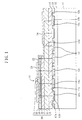
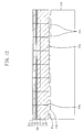
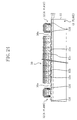
- Figure 1 shows the sectional structure of a gallium nitride-based semiconductor laser diode according to this embodiment.
- a seed layer 12 of gallium nitride (GaN) for ELOG is formed with a low temperature buffer layer (not shown) of GaN sandwiched therebetween.
- Convexes 12a in the shape of stripes extending at intervals along a substrate surface direction are formed in an upper portion of the seed layer 12 , and a mask film 13 of silicon nitride (SiN x ) is formed on the bottom and the walls of each concave (groove) 12b formed between the convexes 12a .
- SiN x silicon nitride
- a selectively grown layer 14 of GaN is formed so as to be in contact with the respective convexes 12a and to have gaps 12c between its lower face and the bottoms of the grooves 12b .
- a lamination body 30 consisting of plural nitride semiconductor layers including double heterojunction of the laser diode is formed.
- the lamination body 30 includes an n-type contact layer 15 of n-type GaN, an n-type cladding layer 16 of n-type Al 0.07 Ga 0.93 N, an n-type light guiding layer 17 of n-type GaN, a multiple quantum well (MQW) active layer 18 including a well layer of Ga 0.8 In 0.2 N with a thickness of approximately 3 nm and a barrier layer of GaN with a thickness of 6 nm, a p-type light guiding layer 19 of p-type GaN, a p-type cladding layer 20 of p-type Al 0.07 Ga 0.93 N and a p-type contact layer 21 of p-type GaN successively formed on the selectively grown layer 14 .
- MQW multiple quantum well
- the energy gap of the well layer containing indium and included in the MQW active layer 18 is smaller than the energy gap of the n-type and p-type cladding layers 16 and 20 containing aluminum.
- the refractive index is the largest in the well layer of the MQW active layer 18 and is smaller in the order of the light guiding layers 17 and 19 and the cladding layers 16 and 20.
- An upper portion of the p-type cladding layer 20 and the p-type contact layer 21 is formed into a ridge 31 working as a current confining portion corresponding to a current injecting region with a width of approximately 3 through 5 ⁇ m.
- the lamination body 30 including the MQW active layer 18 is etched so as to partly expose the n-type contact layer 15 , and the top face and the side face of the etched lamination body 30 are covered with an insulating film 22 of silicon oxide.
- a p-side electrode 23 including stacked layers of nickel (Ni) and gold (Au) is formed to be in ohmic contact with the p-type contact layer 21 through the opening.
- an n-side electrode 24 including stacked layers of titanium (Ti) and aluminum (Al) is formed so as to be in ohmic contact with the n-type contact layer 15 .
- the ridge 31 is formed in a dislocation low-density region including fewer crystal dislocations positioned above the gap 12c .
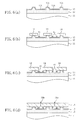
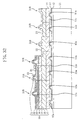
- Figures 2(a), 2(b), 3(a), 3(b) and 4 are sectional views for showing procedures in the method of fabricating the semiconductor laser diode of Embodiment 1.
- TMG trimethyl gallium
- NH 3 ammonia
- the resist film is patterned into stripes by photolithography, thereby forming a resist pattern 40.
- the seed layer 12 is dry etched by using the resist pattern 40 as a mask.
- a cyclic structure including, as one cycle, a convex 12a with a sectional width of approximately 3 ⁇ m and a groove (recess) 12b with a sectional width of approximately 12 ⁇ m is formed in the upper portion of the seed layer 12 .
- a mask film 13 of silicon nitride is deposited on the bottoms and the walls of the grooves 12b of the seed layer 12 and the resist pattern 40 by electron cyclotron resonance (ECR) sputtering.
- ECR electron cyclotron resonance
- solid silicon is used as the raw material of silicon
- nitrogen is used as a reaction gas
- argon is used as plasma gas. Since the ECR sputtering is employed for depositing the mask film 13 , the mask film 13 with high quality can be formed at a low temperature.
- the resist pattern 40 is lifted off, thereby removing the resist pattern 40 and a portion of the mask film 13 deposited on the resist pattern 40 .
- the mask film 13 may cover whole or a part of the wall of the groove 12b .
- a selectively grown layer 14 of GaN is grown on the seed layer 12 by the MOVPE again by using, as the seed crystal, the C plane appearing on the top faces of the convexes 12a exposed from the mask film 13 .
- the selectively grown layer 14 grows upward from the top face of each convex 12a as well as grows along a direction parallel to the substrate surface (i.e., laterally grows). Therefore, the crystals grown from the both sides of each groove 12b meet each other at substantially the center of the groove 12b , so as to form a junction portion 14a .
- an n-type contact layer 15 , an n-type cladding layer 16 , an n-type light guiding layer 17 , a MQW active layer 18 , a p-type light guiding layer 19 , a p-type cladding layer 20 and a p-type contact layer 21 are successively grown, thereby forming a lamination body 30 .
- a ridge 31 for selectively injecting a current into the MWQ active layer 18 is formed from the upper portion of the p-type cladding layer 20 and the p-type contact layer 21 in a dislocation low-density region positioned above the gap 12c and not overlapping the junction portion 14a .
- the lamination body 30 excluding the ridge 31 is dry etched so as to partly expose the n-type contact layer 15 , and an insulating film 22 is deposited on the exposed faces of the lamination body 30 .
- a p-side electrode 23 is formed over and on both sides of the ridge 31 exposed in the opening of the insulating film 22 and an n-side electrode 24 is formed on a portion of the n-type contact layer 15 exposed in the opening of the insulating film 22 by deposition or sputtering.
- a dislocation high-density region 14b with a dislocation density of approximately 1 x 10 9 cm -2 is formed in a portion of the selectively grown layer 14 above the seed crystal, namely, above the convex 12a .
- a laterally grown region of the selectively grown layer 14 is formed into a dislocation low-density region 14c with a dislocation density of approximately 1 x 10 7 cm 2 . Accordingly, when the ridge 31 , namely, the current injecting region serving as a cavity of laser, is formed above the dislocation low-density region 14c of the lamination body 30 , the reliability of the laser diode can be improved.
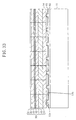
- the grooves 12b in the shape of stripes are formed in the upper portion of the seed layer 12, and the mask film 13 is formed at least on the bottoms of the grooves.
- the selectively grown layers 14 are grown by using, as the seed crystal, the top faces of the convexes 12a sandwiched between the grooves 12b.
- polycrystals 41 of GaN may be deposited on the mask film 13.
- junction portion 14a threading the selectively grown layer 14 and the lamination body 30 shown in Figure 1 along a direction vertical to the substrate surface is formed as a small angle boundary where edge dislocations are collected. Accordingly, although electrons injected from the n-side electrode 24 pass through a plurality of junction portions 14a to reach the MQW active layer 18 , the dislocations collected in the junction portions 14a never prevent the injection of the electrons.
- the cavity facet of a semiconductor laser diode is formed by cleaving the substrate 11 , and flaws and cracks may be caused in the substrate 11 during the cleavage.
- the gaps 12c are provided between the substrate 11 and the lamination body 30 , flaws caused in the substrate 11 can be stopped by the gaps 12c . Accordingly, possibility of damage of the lamination body 30 due to the flaws caused in the substrate 11 can be remarkably reduced.
- the dislocation density of the crystal is as high as approximately 10 9 cm -2 .
- a step on the crystal surface is terminated during step flow growth due to the dislocations, screw dislocations in particular, included at a high density, resulting in forming microfacets on the crystal surface. Accordingly, the crystal surface becomes irregular and the crystal becomes poor in flatness.
- the quantity of a raw material of indium incorporated into the crystal is varied, resulting in causing harmful effects such as increase of the threshold current of the laser diode.
- the MOVPE is used for growing the nitride semiconductor in this embodiment, which does not limit the invention. Any growth method other than the MOVPE such as halide vapor phase epitaxial (HVPE) growth and molecular beam epitaxial (MBE) growth may be used as far as a nitride semiconductor can be grown. This goes for respective embodiments described below.
- HVPE halide vapor phase epitaxial
- MBE molecular beam epitaxial
- the substrate 11 is made from sapphire in this embodiment, for example, silicon carbide, neodymium gallate (NGO), gallium nitride or the like can be used instead of sapphire.
- the low temperature buffer layer is not always necessary as far as the seed layer 12 can be formed in monocrystal.
- any other method can be employed as far as the convexes 12a and the grooves 12b can be formed with the mask film 13 remaining at least on the bottoms of the grooves 12b.
- any method can be employed as far as the C plane of the convexes 12a not covered with the mask film 13 can be used as the seed crystal and the gaps 12c can be formed.
- a mask film for selective growth with an opening pattern in the shape of stripes may be formed on the flat top face of the seed layer 12 so as to grow the convexes projecting from the opening pattern of the mask film.
- the mask film 13 may be formed merely on the bottoms of the grooves 12b as far as the gaps 12c can be formed.
- the mask film 13 is formed from silicon nitride in this embodiment, another dielectric filmor amorphous insulating film may be used instead of the silicon nitride film.
- silicon oxide (SiO 2 ), nitrided silicon oxide (SiON), aluminum oxide (Al 2 O 3 ), nitrided aluminum oxide (AlNO), titanium oxide (TiO 2 ), zirconium oxide (ZrO 2 ) or niobium oxide (Nb 2 O 3 ) may be used. Films of these materials can be comparatively easily formed by the ECR sputtering.
- the selectivity of crystal growth can be improved as compared with the case where the mask film 13 is formed from a dielectric, and hence, deposition of polycrystals 41 on the mask film 13 can be further suppressed.
- the lamination body 30 with high quality can be very easily formed without being affected by the polycrystals 41 .
- Tungsten that is, a metal with a high melting point
- Tungsten is stable in its characteristics owing to its melting point of 3380°C the highest among those of metals and its low vapor pressure. Therefore, an impurity such as silicon and oxygen can be prevented from being mixed in the selectively grown layer 14 differently from the case where a dielectric such as silicon oxide is used. As a result, a deep level and a non-luminescent center are never formed in the selectively grown layer 14 formed by using the mask film 13 of tungsten.
- Figure 7 shows comparison in photoluminescence at room temperature between a selectively grown layer 14 formed by using a mask film 13 of a dielectric and a selectively grown layer 14 formed by using a mask film 13 of a metal with a high melting point.
- the selectively grown layer 14 of Modification 1 As is shown in Figure 7 , in the selectively grown layer 14 of Modification 1, there is no luminescence at a deep level of a wavelength of approximately 430 nm, and very strong luminescence can be obtained at the end of the band. This reveals that the selectively grown layer 14 of Modification 1 has higher quality than the selectively grown layer 14 of Embodiment 1. Accordingly, when the lamination body 30 is grown on the selectively grown layer 14 with such high quality, the MQW active layer 18 can attain higher luminous efficiency.
- tungsten is used for the mask film 13 of Modification 1
- another metal with a high melting point or a metal compound with a high melting point may be used instead.
- molybdenum (Mo), niobium (Nb), tungsten silicide (WSi x ), molybdenum silicide (MoSi x ) or niobium silicide (NbSi x ) may be used. Films of these materials can be comparatively easily formed by electron beam deposition or sputtering.
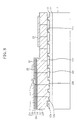
- Figure 8 shows the sectional structure of a gallium nitride-based semiconductor laser diode according to Modification 2 of Embodiment 1.
- like reference numerals are used to refer to like elements shown in Figure 1 so as to omit the description.
- the n-side electrode 24 is provided on an exposed portion of the n-type cladding layer 16 .
- Figure 9 shows the sectional structure a gallium nitride-based semiconductor laser diode using the M plane as a cavity facet according to Embodiment 2.
- like reference numerals are used to refer to like elements shown in Figure 1 so as to omit the description.
- an n-type contact layer 15 is characterized by being directly formed by using, as a seed crystal, monocrystal nuclei generated on the C plane of the respective convexes 11a of the substrate 11A .
- Figures 10(a), 10(b) , 11 and 12 are sectional views for showing procedures in the method of fabricating the semiconductor laser diode of Embodiment 2.
- a resist pattern 40 in the shape of stripes extending along the A-axis of the substrate 11A with a cycle of approximately 10 through 30 ⁇ m.
- the resist pattern 40 as a mask, grooves 11b each with a sectional width of approximately 9 through 27 ⁇ m and a depth of approximately 20 through 500 nm are formed in an upper portion of the substrate 11A by dry etching such as reactive ion etching (RIE).
- RIE reactive ion etching
- a convex 11a formed between the grooves 11b has a sectional width of approximately 1 through 3 ⁇ m.
- the resist pattern 40 is removed, so as to obtain the substrate 11A having, in its upper portion, the convexes 11a in the shape of stripes extending along the A-axis.
- TMG trimethyl gallium
- NH 3 ammonia
- SiH 4 silane
- the crystals grown from the both sides of the groove 11b meet each other so as to form a junction portion 15a at substantially the center of the groove 11b .
- the crystals grown from the top faces of the plural convexes 11a are integrated, so as to form the n-type contact layer 15 having the C plane as the top face.
- plural gaps 11c are formed so as to be surrounded with the bottoms and the walls of the respective grooves 11b and the lower face of the n-type contact layer 15.
- nitride semiconductor in general on a substrate having a different lattice constant from the nitride semiconductor, if GaN crystal is directly grown on the substrate without forming a low temperature buffer layer of a nitride semiconductor therebetween, merely a three-dimensional film including a combination of monocrystal nuclei of GaN is formed.
- the dry etching is employed for forming the grooves 11b of the substrate 11A , damage layers derived from the dry etching are formed on the bottoms and the walls of the grooves 11b . Therefore, generation of the monocrystal nuclei are prevented on the bottoms and the walls of the grooves 11b .
- the top face of each convex 11a not subjected to the dry etching has a small sectional width of approximately 1 through 3 ⁇ m, and hence, monocrystal nuclei with a high density can be easily generated thereon. In this manner, the monocrystal nuclei generated on the top faces of the convexes 11a work as the seed crystal for the selective growth, resulting in accelerating the selective growth along the substrate surface direction under the aforementioned conditions.
- n-type contact layer 15 depends upon the width and the like of the groove 11b and is herein approximately 2 through 6 ⁇ m. Also, a tilt angle between the C-axis in a portion of the n-type contact layer 15 above the convex 11a and the C-axis in a portion thereof above the gap 11c is suppressed to 0.01 through 0.03 degree.
- the tilt angle can be thus very small in the ELOG of this embodiment as compared with that in the conventional ELOG because the n-type contact layer 15 corresponding to the crystal layer formed through the ELOG is not in contact with the substrate 11A , and hence, stress as in the conventional ELOG is not applied to the interface with the mask film 13.
- a void in the shape of a reverse V having an opening on the gap 11c is formed in a lower portion of the junction portion 15a .
- the polycrystals are deposited on the bottoms of the grooves 11b in the selective growth of the n-type contact layer 15, the polycrystals are never in contact with the n-type contact layer 15 owing to a level difference caused between the convex 11a and the groove 11b formed in the upper portion of the substrate 11A. Therefore, the crystal quality of the lamination body 30 is never harmfully affected. As a result, variation in the operation characteristic of the laser diode including the lamination body 30 can be reduced, so as to improve the yield.
- the rest of semiconductor layers of the lamination body 30 are formed on the n-type contact layer 15 .
- an n-type cladding layer 16 After setting the substrate temperature to, for example, approximately 970°C, an n-type cladding layer 16, an n-type light guiding layer 17 , a MQW active layer 18, a p-type light guiding layer 19 , a p-type cladding layer 20 and a p-type contact layer 21 are successively grown on the n-type contact layer 15 in a mixed atmosphere of hydrogen and nitrogen at a pressure of approximately 300 Torr.
- the MQW active layer 18 includes a well layer of Ga 0.92 In 0.08 N with a thickness of approximately 4 nm and a barrier layer of GaN with a thickness of approximately 6 nm.
- the ridge 31 has a width of approximately 2 through 5 ⁇ m.
- GaN crystal is transparent against visible light, it is easy to distinguish the convex 11a from the gap 11c with an optical microscope. Therefore, in determining the position of the ridge 31 in the photolithography, there is no need to use a dedicated alignment pattern.
- an insulating film 22 is deposited on the exposed faces of the lamination body 30 .
- a p-side electrode 23 is formed on the insulating film 22 so as to extend over the ridge 31 and cover a portion of the p-type contact layer 21 exposed from the insulating film 22.
- an n-side electrode 24 is formed on a portion of the n-type contact layer 15 exposed from the insulating film 22 .
- the substrate 11A is cleaved on the M plane of the lamination body 30 , namely, on it's A plane, thereby forming a cavity facet.
- the A plane of sapphire is a crystal plane difficult to cleave as described above, even when the sapphire crystal is broken with the cleavage shifted from a predetermined position, the breakage is prevented from being propagated to the lamination body 30 owing to the gaps 11c formed in the substrate 11A. Accordingly, a good cleaved end can be easily obtained in the vicinity of the cavity facet. The yield in the cleavage of the laser diode can be thus improved.
- the cleaved end of the cavity is coated with a dielectric film or the like so as to attain appropriate reflectance, and thereafter, the substrate is divided along a plane parallel to the ridge 31 into chips so as to obtain semiconductor laser diodes.
- the semiconductor laser diode of this embodiment uniform step flow growth is observed in the ELO grown region as described in Embodiment 1.
- the MQW active layer 18 is grown on such a flat surface, local segregation of indium can be avoided.
- the MQW active layer 18 is formed as a high quality crystal, so as to reduce the operation current of the laser diode.
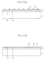
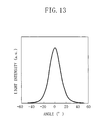
- Figure 13 shows a far-field pattern, in a direction parallel to the cavity facet, of laser emitted from the semiconductor laser diode of this embodiment, and thus, a unimodal distribution of light intensity can be satisfactorily obtained.
- the far-field pattern of the semiconductor laser diode of Conventional Example 1 exhibits a multimodal distribution of light intensity as shown in Figure 42 .
- the semiconductor laser diode of this embodiment attains the unimodal distribution because the gaps 11c provided between the lamination body 30 and the substrate 11A can optically separate the lamination body 30 and the substrate 11A from each other.
- the n-type contact layer 15 having a large refractive index than the n-type cladding layer 16 is formed under the n-type cladding layer 16, light generated in the MQW active layer 18 can easily leak to the substrate 11A .
- the gaps 11c with a very small refractive index are formed below the n-type contact layer 15 , a parasitic waveguide is never formed between the n-type cladding layer 16 and the substrate 11A. As a result, the light confinement coefficient of the MQW active layer 18 is never lowered by the leakage of the generated light.
- This effect to suppress the formation of a parasitic waveguide depends upon a dimension of the gap 11c along a direction vertical to the substrate surface, namely, the depth of the groove 11b . According to computer simulation, it is confirmed that the leakage of light to the substrate 11A can be substantially avoided when the depth of the groove 11b is at least approximately 50 nm.
- the n-type contact layer 15 of GaN includes 2% or more of aluminum, the leakage of light to the substrate 11A can be more effectively avoided.
- the optimal conditions for the ELOG can be appropriately selected in accordance with the composition of the mixed crystal.
- the substrate 11A is made from silicon carbide, gallium nitride or the like may be used instead of sapphire.
- the substrate 11A is made from silicon carbide, tensile strain is applied to the lamination body 30 so as to easily cause cracks. Therefore, it is preferred in this case that the integrated n-type contact layer 15 has a thickness smaller than 2 ⁇ m by setting the sectional width of each groove 11b as small as possible.
- the substrate 11A is made from silicon carbide or gallium nitride, although it can be easily cleaved on the M plane as well as A plane, the yield can be improved by cleaving the substrate on a plane perpendicular to the direction of the stripes of the grooves 11b .
- any other dry etching method such as ion milling, may be employed as far as a damage layer can be formed on the bottoms and the walls of the grooves 11b so as to selectively grow a gallium nitride-based semiconductor.
- the damage layer formed in the grooves 11b is used as a mask layer for the ELOG in this embodiment.
- a mask film of silicon nitride or the like is preferably formed at least on the bottoms of the grooves 11b so as to further improve the selectivity.
- the material for the mask film 13 is not limited to silicon nitride but may be a dielectric or amorphous insulator as described in Embodiment 1, and is preferably a metal with a high melting point or a metal compound with a high melting point as described in Modification 1 of Embodiment 1.
- the invention is applied to a laser diode in this embodiment as described so far, but the invention can be applied to a method of growing a semiconductor for obtaining a gallium nitride-based crystal with a low dislocation density. Furthermore, since the seed layer 12 formed on the substrate 11 in Embodiment 1 is not used in this embodiment, the fabrication process can be simplified.
- a light emitting device not only a light emitting device but also another semiconductor device such as an electronic device can be fabricated by using the nitride semiconductor layer including a dislocation low-density region of this embodiment. In this manner, the reliability and the yield of the semiconductor device can be improved.
- Figure 14 shows the sectional structure of a gallium nitride-based semiconductor laser diode according to Embodiment 3.
- like reference numerals are used to refer to like elements shown in Figure 1 so as to omit the description.
- Aluminum gallium nitride (AlGaN) is used for a selectively grown layer 14A grown from the top faces of the respective convexes 12a of the seed layer 12 to be integrated, and an n-type superlattice cladding layer 16A having a superlattice structure including n-type AlGaN and n-type GaN also serves as the n-type contact layer 15.
- AlGaN Aluminum gallium nitride
- Figure 15 shows the relationship between the distribution of a refractive index on the ridge along a direction vertical to the substrate surface and the distribution of light intensity on a cavity facet in the semiconductor laser diode of this embodiment.
- Figure 16 shows a far-field pattern, along a direction parallel to the cavity facet, of laser emitted from the semiconductor laser diode of this embodiment.
- each groove 12b of the seed layer 12 has a depth of approximately 50 nm, and the n-type superlattice cladding layer 16A has an average composition of Al 0.07 Ga 0.93 N. Furthermore, the structure of the lamination body above the n-type light guiding layer 17 is the same as that of the conventional semiconductor laser diode shown in Figure 37 .
- the MQW active layer 18 is separated from the substrate 11 by the gaps 12c of the seed layer 12 and the selectively grown layer 14A of n-type AlGaN having a refractive index smaller than or equal to the n-type superlattice cladding layer 16A is provided between the n-type superlattice cladding layer 16A and the seed layer 12 . Accordingly, no parasitic waveguide is formed between the n-type superlattice cladding layer b and the substrate 11 , and the light confinement coefficient of the MQW active layer 18 can be suppressed from being lowered due to the leakage of the generated light.
- This effect to suppress the formation of a parasitic waveguide depends upon a dimension of the gap 11c along a direction vertical to the substrate surface, namely, the depth of the groove 11b . As described above, it is confirmed that the leakage of light to the substrate 11 can be substantially avoided when the depth of the groove 11b is at least approximately 50 nm.
- the selectively grown layer 14A includes 2% or more and preferably 4% or more aluminum, the leakage of light to the substrate 11 can be suppressed.
- the crystallinity of the selectively grown layer 14A is never degraded by the polycrystals because there is a level difference between the top face of the convex 12a serving as the seed crystal and the bottom of the groove 12b where the polycrystals are deposited.
- the variation in the crystallinity of the lamination body 30 can be largely reduced, so as to improve the yield in the fabrication of semiconductor laser diodes.
- Figure 17 shows a plane photograph of the selectively grown layer 14A prior to the formation of the lamination body 30 obtained with an optical microscope and the corresponding sectional structure of the selectively grown layer 14A .
- a dislocation low-density region 14c can be easily distinguished from a dislocation high-density region 14b and a junction portion 14a with the optical microscope. Accordingly, in a procedure for aligning the ridge 31 in the photolithography, there is no need to use a dedicated alignment pattern (alignment mark).
- the n-side electrode 24 is in contact with the n-type superlattice cladding layer 16A and the n-type superlattice cladding layer 16A also serves as the n-type contact layer.
- the n-type contact layer on which the n-side electrode 24 is formed is made from a bulk layer (single layer) including aluminum in a large composition ratio, for example, a single layer of n-type Al 0.o7 Ga 0.93 N, the driving voltage of the laser diode is increased because the resistivity of the single layer is increased to approximately twice of that of gallium nitride or the contact resistance is increased.
- the present inventors have found that the specific resistance of the n-type superlattice cladding layer 16A including, for example, n-type Al 0.14 Ga 0.86 N and n-type GaN is substantially equal to that of a single layer of n-type GaN. This is because of large mobility of two-dimensional electron gas generated in the superlattice semiconductor layer. Furthermore, the present inventors have found that the contact resistance of the superlattice semiconductor layer can be substantially equal to that of an n-type GaN layer when the thickness of a unit layer included in the superlattice structure is sufficiently small, for example, is approximately 2 nm. At this point, the doping concentration of the n-type impurity is approximately 1 x 10 18 cm -3 .
- the superlattice layer preferably includes aluminum in an average ratio of 2% and has a thickness of ⁇ /(4n) or less, wherein ⁇ indicates the wavelength of light and n indicates the refractive index of the unit layer.
- the substrate 11 is made from sapphire, for example, silicon carbide, neodymium gallate (NGO), gallium nitride or the like may be used instead of sapphire.
- the convexes 12a in the seed layer 12 are formed by the lift-off method, any other method may be employed as far as the convexes 12a and the grooves 12b can be formed with the mask film 13 remaining on at least the bottoms of the grooves 12b .
- the mask film 13 may be formed on the bottoms of the grooves 12b alone as far as the gaps 12c can be formed.
- the mask film 13 may be formed from a dielectric such as silicon nitride and silicon oxide by the ECR sputtering, and preferably, is formed from a metal with a high melting point such as tungsten or its silicide.
- Figure 18 shows the sectional structure of a gallium nitride-based semiconductor laser diode of Embodiment 4.
- like reference numerals are used to refer to like elements shown in Figure 1 so as to omit the description.
- the selectively grown layer 14A of AlGaN of Embodiment 3 is formed to have a two-layer structure including a first selectively grown layer 14B of GaN formed in the vicinity of the top faces of the convexes 12a of the seed layer 12 and a second selectively grown layer 14C of AlGaN for covering the top and side faces of the first selectively grown layer 14B as is shown in Figure 18 .
- the n-type superlattice cladding layer 16A also serving as the n-type contact layer is formed to have a two-layer structure including an n-type superlattice contact layer 15A and an n-type cladding layer 16 of a single Al 0.07 Ga 0.93 N layer.
- the n-type superlattice contact layer 15A has a superlattice structure including n-type Al 0.1 Ga 0.9 N and n-type GaN.
- the p-side electrode 23 is formed merely on the top face of the ridge 31 formed in the upper portion of the lamination body 30 , and a p-side line electrode 25 is formed so as to cover the p-side electrode 23 and the ridge 31 .
- the n-side electrode 24 is covered with an n-side line electrode 26 .
- first selectively grown layers 14B are grown by using, as the seed crystal, the top faces of the convexes 12a of the seed layer 12 .
- the growth pressure for the first and second selectively grown layers 14B and 14C is set to a comparatively low pressure of approximately 200 Torr until the second selectively grown layers 14C grown by using, as the seed crystal, the first selectively grown layers 14B are integrated.
- the growth rate of the first and second selectively grown layers 14B and 14C is larger in the A-axis direction of the seed layer 12 , namely, in a direction crossing the grooves 12b, than in the C-axis direction vertical to the substrate surface.
- the MQW active layer 18 is grown at a high pressure of approximately 300 Torr. This is because as the growth pressure is higher, indium with a high vapor pressure can be suppressed to evaporate, so that the MQW active layer 18 can attain higher crystal quality. Accordingly, in forming the lamination body 30 , the growth pressure is changed from that for growing the first and second selectively grown layers 14B and 14C .
- one crystal growth furnace capable of changing the growth pressure during its operation may be used, or plural crystal growth furnaces respectively set to different growth pressures may be used.
- the semiconductor laser diode of Embodiment 4 exhibits, similarly to that of Embodiment 3, the refractive index distribution and the light intensity distribution as shown in Figure 15 and attains the far-field pattern of emitted light as shown in Figure 16.
- the MQW active layer 18 is separated from the substrate 11 by the gaps 12c of the seed layer 12, and the n-type superlattice contact layer 15A and the second selectively grown layer 14C having a refractive index smaller than or equivalent to the n-type cladding layer 16A is formed between the n-type cladding layer 16 and the seed layer 12 . Accordingly, no parasitic waveguide is formed between the n-type cladding layer 16 and the substrate 11 , and the light confinement coefficient of the MQW active layer 18 can be suppressed from being reduced due to the leakage of the generated light.
- the light leakage to the substrate 11 can be substantially avoided when the depth of the groove 12b is at least approximately 20 nm.
- the second selectively grown layer 14C includes 2% or more and preferably 4% or more of aluminum, the leakage of the generated light to the substrate 11 can be suppressed.
- the light confinement coefficient of the MQW active layer 18 is approximately 1.5 times as large as that shown in Figure 41 , resulting in reducing the threshold current of the laser diode.
- Figure 19(a) schematically shows the selective growth mechanism of Embodiment 4 and Figure 19(b) schematically shows the selective growth mechanism of Conventional Example 2.
- the selectively grown layer 14A of AlGaN includes 4% or more of aluminum
- roughness 14d may be caused at the end in the growing direction of the selectively grown layer 14A as is shown in Figure 20(b).
- Such roughness may be rather suppressed by appropriately setting the growth conditions for the selectively grown layer 14A, such as a growth pressure, a growth temperature and a V/III ratio, that is, a molar ratio between a group III element source and a group V element source.
- the roughness 14d at the growth end is preferably minimized as far as possible.
- a nitride semiconductor layer including aluminum in a small composition ratio is preferably used for the selectively grown layer formed by using the seed layer 12 as the seed crystal.
- the first selectively grown layer 14B of a gallium nitride-based semiconductor including 4% or less of aluminum is first grown in the vicinity of the convexes 12a of the seed layer 12 , and then, the second selectively grown layer 14C of a gallium nitride-based semiconductor including more than 4% of aluminum and having a small refractive index is grown by using the first selectively grown layer 14B as the seed crystal. In this manner, the second selectively grown layer 14C can be satisfactorily laterally grown without causing the roughness 14d at the growth end.
- composition ratio of aluminum is larger in the second selectively grown layer 14C and as the growth time is longer, more polycrystals 41 are deposited on the mask film 13 . This is because the evaporation rate of the AlGaN crystal or the AlN crystal is smaller than that of the GaN crystal.
- the quantity of the reaction seed supplied onto the mask film 13 can be reduced. Accordingly, the quantity of the polycrystals 41 deposited on the mask film 13 can be largely reduced, so as to minimize the harmful effect on the lamination body 30 grown above the gaps 12c . As a result, the light confinement coefficient can be definitely increased, and the production yield can be definitely improved because the crystallinity of the lamination body 30 is so improved that the variation in the operation characteristic of the laser diode is largely reduced.
- the substrate 11 is made from sapphire in this embodiment, for example, silicon carbide, neodymium gallate, gallium nitride or the like may be used instead of sapphire.
- the mask film 13 can be formed merely on the bottoms of the grooves 12b as far as the gaps 12c can be formed.
- the mask film 13 may be formed from a dielectric such as silicon nitride and silicon oxide by the ECR sputtering, and more preferably, is formed from a metal with a high melting point such as tungsten or its silicide.
- Figures 22 and 23 show a gallium nitride-based semiconductor laser diode according to Embodiment 5, wherein Figure 22 shows the sectional structure taken on the M plane of a lamination body, namely, the A plane of a substrate, and Figure 23 shows the sectional structure taken on line XXIII-XXIII of Figure 22 corresponding to the A plane of the lamination body, namely, the M plane of the substrate.
- Figures 22 and 23 like reference numerals are used to refer to like elements shown in Figure 1 so as to omit the description.
- Embodiment 5 is characterized by definitely fabricating a semiconductor laser diode with a flat cavity facet 32 by using the lamination body 30 including the MQW active layer 18 .
- a cyclic structure including, as one cycle, the convex 12a with a sectional width of approximately 3 ⁇ m and the groove 12b with a sectional width of approximately 12 ⁇ m is formed, and every 34 cycles (corresponding to a length of 510 ⁇ m) of the cyclic structure, an enlarged groove 12d with an enlarged sectional width of approximately 20 ⁇ m is formed.
- the lamination bodies 30 laterally grown by using the top faces of the respective convexes 12a of the seed layer 12 as the seed crystal are not integrated above the enlarged groove 12d . Therefore, the A planes of the adjacent lamination bodies 30 appear above the enlarged groove 12d without being in contact with each other.
- These growth ends are naturally formed crystal planes, and includes no other surface orientations such as the M plane. Accordingly, when such a growth end is used as the cavity facet 32, the mirror loss on the cavity facet derived from mixture of the A plane and the M plane as in the conventional semiconductor laser diode of Figure 43 can be avoided.
- the P-type light guiding layer 19 and the p-type cladding layer 20 with larger energy gap than the MQW active layer 18 can be formed on the cavity facet 32 . Therefore, emitted light is never absorbed at the ends of the p-type light guiding layer 19 and the p-type cladding layer 20 . As a result, the temperature increase in the lamination body 30 in the vicinity of the cavity facet 32 can be suppressed, and hence, the reliability can be prevented from degrading due to degradation of the facet.
- the ELOG using the top faces of the convexes 12a in the shape of stripes as the seed crystal is employed, and the enlarged grooves 12d are formed in a cycle larger than that of the grooves 12b formed by the side faces of the convexes 12a . Therefore, the growth end of the lamination body 30 is directly exposed above the enlarged groove 12d, and hence, the naturally formed exposed end can be formed into the cavity facet 32 .
- the threshold value of the laser diode of this embodiment is lower by approximately 30% than that of the conventional laser diode.
- the substrate 11 is formed from sapphire in this embodiment, forexample, siliconcarbide, neodymiumgallate (NGO), gallium nitride or the like may be used instead of sapphire.
- the mask film 13 may be formed merely on the bottoms of the grooves 12b as far as the gaps 12c can be formed.
- the mask film 13 may be formed from a dielectric such as silicon nitride and silicon oxide by the ECR sputtering, and more preferably, is formed from a metal with a high melting point such as tungsten or its silicide.
- the widths of the convex 12a and the groove 12b formed in the upper portion of the seed layer 12 are not limited to 3 ⁇ m and 12 ⁇ m, respectively but the convex 12a preferably has a smaller width than the groove 12b. In this manner, the influence of dislocations propagated from the seed crystal on the top faces of the convexes 12a to the lamination body 30 can be reduced, and the degradation of the laser operation characteristics due to the dislocations can be prevented, resulting in improving the reliability of the laser diode.
- the cycle of forming the enlarged grooves 12d in the upper portion of the seed layer 12 may be set to an appropriate value in accordance with the length of the cavity.
- the stripe direction of the convexes 12a is set to the M-axis direction of the lamination body 30 so as to use the naturally formed A plane as the cavity facet 32 .
- the M plane can be naturally formed. Accordingly, when the convexes 12a are formed in the shape of stripes extending along the A-axis direction, a highly reliable semiconductor laser diode including the naturally formed M plane as the cavity facet 32 and having a largely reduced threshold current can be obtained.
- Figure 24 shows the sectional structure of a gallium nitride-based semiconductor laser diode of Modification 1 of Embodiment 5 taken on the M plane of a lamination body, namely, the A plane of a substrate.
- like reference numerals are used to refer to like elements shown in Figure 22.
- an enlarged groove 12d with an enlarged sectional width of approximately 20 ⁇ m is formed on the inside of and adjacent to the enlarged groove 12d for naturally forming the cavity facet 32 of the lamination body 30 . Accordingly, side gaps 30a having the A plane as the opposing faces are formed on both sides of the lamination body 30 close to the cavity facets.
- the side gap 30a having a refractive index of 1 and the lamination body 30 of a gallium nitride-based semiconductor having a refractive index of approximately 2.6 are combined to form the cavity facet 32, a large difference in the refractive index can be obtained. Accordingly, the reflectance of a laser beam on the cavity facet 32 can be increased as compared with the case where the cavity facet is coated with a dielectric film or the like.
- an isolation body isolated from the lamination body 30 by the side gap 30a preferably has a lateral dimension, along the light emitting direction, of an integral multiple of ⁇ /(4n), wherein ⁇ indicates the wavelength of light and n indicates the refractive index of the isolation body.
- the side gaps 30a are formed on both sides of the lamination body 30 in this modification, the side gap 30a may be formed on either side of the lamination body 30 for increasing the reflectance so as to increase the output power of emitted light.
- the threshold current for laser action is reduced by approximately 20% as compared with the case where the side gaps 30a are not formed, and thus, the effect attained by the side gaps 30a is remarkable.
- the lamination body 30 may include three or more side gaps 30a .
- Figure 25 shows Modification 2 of Embodiment 5, wherein all the grooves in the shape of stripes formed in the upper portion of the seed layer 12 are formed as enlarged grooves 12d .
- plural lamination bodies 30 are all isolated from one another on the substrate 11 . Accordingly, when a cavity is formed from plural isolation bodies so as to obtain a desired cavity length and the substrate 11 is divided in a side gap 30a in a position corresponding to the facet of the thus formed cavity, one semiconductor laser diode including plural isolation bodies can be obtained.
- the semiconductor laser diode of Modification 2 has a very flat A plane free from irregularities causing mirror loss of a laser beam, and when the number of isolation bodies included in the laser diode is changed, the cavity length can be easily changed.
- a selectively grown seed layer 34 is integrally formed through the ELOG.
- convexes 34a and grooves 34b are formed in an equivalent cycle of the convexes 12a and the grooves 12b of the seed layer 12 , and a second mask film 13B is formed on the bottoms and the walls of the grooves 34b .
- the convexes 34a are formed above the grooves 12b so as to be formed neither in a dislocation low-density region nor in a junction portion of the selectively grown seed layer 34.
- the selectively grown layer 14 is grown by using, as the seed crystal, the C plane on the top faces of the convexes 34a formed in the upper portion of the selectively grown seed layer 34 .
- On the top face of the convex 34a appears a high quality crystal face free from not only dislocations derived from the seed crystal on the top face of the convex 12a of the seed layer 12 but also a defect derived from the junction portion of the selectively grown seed layer 34 .
- the lamination body 30 formed on the high quality selectively grown layer 14 is free from defectives. Accordingly, it is possible to avoid loss resulting from scatter of a laser beam due to a crystal defective and degradation of the reliability through a non-luminescent process of carriers.
- this modification realizes a very high quality gallium nitride-based semiconductor laser diode.
- Figure 27 shows the sectional structure of a gallium nitride-based semiconductor laser diode of Embodiment 6 taken on the A plane of a lamination body, namely, the M plane of a substrate.
- like reference numerals are used to refer to like elements used in Embodiment 3 shown in Figure 14 so as to omit the description.
- a first seed layer 12A and a second seed layer 12B are formed on the substrate 11 of sapphire.
- convexes 12a and grooves 12b in the shape of stripes are formed in parallel to the M plane of the substrate 11 , namely, the A plane of the lamination body 30 .
- the convexes 12a and the grooves 12b in the shape of stripes are formed in parallel to the convexes 12a and the grooves 12b of the first seed layer 12A so as not to overlap them in a direction vertical to the substrate surface.
- Figures 28(a), 28(b), 29(a), 29(b), 30(a), 30(b) and 31 are sectional views taken on the A plane of the substrate for showing procedures in the method of fabricating the semiconductor laser diode of this embodiment.
- a low temperature buffer layer (not shown) of GaN is deposited on a substrate 11 having the C plane as the principal plane by the MOVPE by supplying TMG as a group III element source and NH 3 as a nitrogen source with the substrate temperature set to approximately 530°C in a mixed atmosphere of hydrogen and nitrogen, for example, at a pressure of approximately 300 Torr.
- TMG a group III element source
- NH 3 a nitrogen source
- the substrate temperature set to approximately 530°C in a mixed atmosphere of hydrogen and nitrogen, for example, at a pressure of approximately 300 Torr.
- TMG, NH3 and SiH4 are supplied onto the substrate 11 , thereby growing a first seed layer 12A of n-type GaN with a thickness of approximately 0.5 through 1 ⁇ m.
- the principal plane of the first seed layer accords with the C plane, and the order of a dislocation density is 10 9 cm -2 .
- the resist film is patterned by the photolithography into stripes extending along the M-axis direction of the first seed layer 12A , thereby forming a resist pattern 40 .
- the first seed layer 12A is dry etched, thereby forming, in an upper portion of the first seed layer 12A, a cyclic structure including, as one cycle, a convex 12a with a sectional width of approximately 3 through 6 ⁇ m and a groove 12b with a sectional width of approximately 12 through 24 ⁇ m.
- the groove 12b has a depth of approximately 50 nm through 1 ⁇ m.
- a mask film 13 of silicon nitride is deposited on the bottoms and the walls of the grooves 12b of the first seed layer 12A and the resist pattern 40 by the ECR sputtering.
- solid silicon is used as the raw material for silicon
- nitrogen is used as a reaction gas
- argon is used as plasma gas.
- the resist pattern 40 is lifted off, thereby removing the resist pattern 40 and a portion of the mask film 13 deposited on the resist pattern 40 .
- the mask film 13 may cover whole or a part of the wall of the groove 12b .
- TMG, NH 3 and SiH 4 are supplied onto the first seed layer 12A by the MOVPE again in a mixed atmosphere of hydrogen and nitrogen, for example, at a pressure of approximately 100 Torr, so as to grow a second seed layer 12B of n-type GaN by using, as the seed crystal, portions of the first seed layer 12A exposed from the mask film 13.
- the second seed layer 12B grows upward from the top faces of the convexes 12a as well as laterally grows in a direction parallel to the substrate surface.
- the crystals grown from the both sides of the groove 12b meet at substantially the center of the groove 12b so as to form a junction portion 12e .
- the respective crystals grown from the top faces of the plural convexes 12a are integrated one another, so as to form the second seed layer 12B having the C plane as the top face.
- plural gaps 12c are formed to be surrounded with the bottoms and the walls of the grooves 12b of the first seed layer 12A and the lower face of the second seed layer 12B .
- the thickness of the second seed layer 12B depends upon the width and the like of the groove 12b and is approximately 2 through 6 ⁇ m.
- a tilt angle between the C-axis in a portion of the second seed layer 12B above the convex 12a and the C-axis in a portion thereof above the gap 12c is 0.01 through 0.03 degree.
- the tilt angle is thus very small in the ELOG of this embodiment as compared with that in the conventional ELOG because the second seed layer 12B corresponding to a crystal layer formed through the ELOG is not in contact with the first seed layer 12A and hence no stress is applied to the interface with the mask film 13 differently from the conventional ELOG.
- a void in the shape of a reverse V having an opening on the gap 12c is formed in a lower portion of the junction portion 12e .
- the polycrystals are not in contact with the second seed layer 12B owing to a level difference caused by the convexes 12a and the grooves 12b formed in the upper portion of the first seed layer 12A , and hence do not harmfully affect the crystallinity of a lamination body 30 including the laser structure.
- the variation in the operation characteristics of the laser diode including the lamination body 30 can be reduced, so as to improve the yield.
- a cyclic structure including, as one cycle, the convex 12a and the groove 12b is formed in the upper portion of the second seed layer 12B in the same manner as in the first seed layer 12A.
- the convexes 12a of the second seed layer 12B are formed so as to have their top faces positioned above the dislocation low-density regions of the second seed layer 12B .
- the top faces of the convexes 12a of the second seed layer 12B are formed in positions different from the top faces of the convexes 12a of the first seed layer 12A in a direction along the substrate surface and on sides of the junction portions 12e .
- the second ELOG can be conducted by using, as the seed crystal, the dislocation low-density regions of the second seed layer 12B positioned above the gaps 12c of the first seed layer 12A. Since a gallium nitride-based crystal is transparent against visible light, the convex 12a and the groove 12b can be easily identified from each other with an optical microscope. Therefore, there is no need to use a dedicated alignment pattern in determining the positions of the convexes 12a in the stripe pattern in the photolithography.
- selectively grown layers 14A of n-type AlGaN having the C plane as the principal plane are grown to be integrated on the second seed layer 12B by the MOVPE in, for example, a mixed atmosphere of hydrogen and nitrogen at a pressure of approximately 100 Torr at a substrate temperature of approximately 1000°C by using, as the seed crystal, the C plane appearing on the top faces of the convexes 12a exposed from the mask film 13.
- the dislocation density is as small as approximately 1 x 10 6 cm -2 .
- an n-type superlattice cladding layer 16A , an n-type light guiding layer 17 , a MQW active layer 18 , a p-type light guiding layer 19, a p-type cladding layer 20 and a p-type contact layer 21 are successively grown on the integrated selectively grown layer 14A , so as to form the lamination body 30.
- the MQW active layer 18 includes, for example, a well layer of Ga 0.92 In 0.08 N with a thickness of approximately 4 nm and a barrier layer of GaN with a thickness of approximately 6 nm, so as to show laser action at a wavelength of 400 nm band.
- a ridge 31 with a width of 2 through 5 ⁇ m for selectively injecting a current into the MQW active layer 18 is formed in the A-axis direction of the lamination body 30 , namely, in a direction perpendicular to the direction of the stripes of the convexes 12a by the dry etching from an upper portion of the p-type cladding layer 20 and the p-type contact layer 21 .
- the lamination body 30 excluding the ridge 31 is dry etched, so as to partly expose the n-type superlattice cladding layer 16A , and an insulating film b is deposited on the exposed faces of the lamination body 30 . Then, openings are formed in the insulating film 22 in positions on the ridge 31 and the n-type superlattice cladding layer 16A.
- a p-side electrode 23 is formed on a portion on the ridge 31 exposed in the opening of the insulating film 22 and around the ridge 31
- an n-side electrode 24 is formed on a portion of the n-type superlattice cladding layer 16A exposed in the opening of the insulating film 22 by the evaporation or the sputtering.
- a cavity facet is formed through the cleavage on the A plane of the lamination body 30, namely, on the M plane of the substrate 11 of sapphire. Since the M plane of sapphire can be easily cleaved, the yield in the cleavage of the semiconductor laser diode can be satisfactorily retained. Although the plural gaps 12c in two stages extending in parallel to the cleaved end are present between the substrate 11 and the lamination body 30, these gaps 12c never lower the yield in the cleavage.
- the cleaved end is coated with a dielectric or the like so as to attain appropriate reflectance, and the substrate is divided into chips.
- the semiconductor laser diode of Figure 27 is fabricated.
- the cavity formed in the A-axis direction of the lamination body 30 including the MQW active layer 18 is provided in a direction perpendicular to the gaps 12c formed through the selective growth in the shape of stripes extending in the M-axis direction.
- the current injecting region for the MQW active layer 18 extending in the lengthwise direction of the ridge 31 crosses the junction portion 14a of the semiconductor layers.
- dislocations collected in the junction portion 14a can affect the operation of the laser diode. It is, however, confirmed through observation of dislocations within the MQW active layer 18 that threading dislocations are present on the plane uniformly at a density of approximately 1 x 10 6 cm -2 regardless of the junction portion 14a . Accordingly, the current injecting region crossing the junction portion 14a does not harmfully affect the reliability of the semiconductor laser diode.
- a tilt angle is as large as 0.1 degree or more. Therefore, when the width of the gap 12 c is, for example, 12 ⁇ m, a zigzag waveguide with a level difference of 10 nm or more is formed, resulting in increasing the operation current of the laser diode.
- the tilt angle when the tilt angle is 0.05 degree or less, the level difference in the waveguide can be suppressed to approximately 5 nm, and hence, the influence of the zigzag waveguide can be substantially ignored.
- the tilt angle can be suppressed to 0.03 degree or less owing to the lateral growth where the selectively grown layer is grown with forming the gaps 12c, and hence, the formation of the zigzag waveguide can be avoided.
- uniform step flow growth is observed in a laterally grown region of the selectively grown layer 14A.
- the MQW active layer 18 is formed on such a flat face, local segregation of indium can be prevented, so as to obtain the MQW active layer 18 with uniform quality. Accordingly, the operation current can be reduced.
- the far-field pattern, in the direction vertical to the substrate surface, of the semiconductor laser diode of this embodiment is equivalent to that shown in Figure 16, and thus, a unimodal and satisfactory light intensity distribution can be obtained.
- the selectively grown layers 14A grown from the top faces of the convexes 12a of the second seed layer 12B to be integrated are formed from n-type AlGaN, and the n-type superlattice cladding layer 16A having the superlattice structure including n-type AlGaN and n-type GaN also works as the n-type contact layer.
- the light confinement coefficient of the MQW active layer 18 can be largely increased.
- the selectively grown layer 14A includes 2% or more and preferably 4% or more of aluminum, the leakage of light to the substrate 11 can be definitely prevented.
- the optimal growth conditions for the lateral growth are selected in accordance with the composition of the mixed crystal to be used.
- the low temperature buffer layer is formed below the first seed layer 12A, the low temperature buffer layer is not always necessary as far as the first seed layer can be formed in a monocrystal.
- the substrate 11 is made from sapphire, for example, silicon carbide, neodymium gallate (NGO), gallium nitride or the like may be used instead of sapphire.
- the substrate 11 is made from silicon carbide, tensile strain is applied to the lamination body 30 and hence cracks can be easily caused. Therefore, it is preferred in this case that the integrated second seed layer 12B has a thickness smaller than 2 ⁇ m by reducing the sectional width of the groove 12b as far as possible. In this manner, the lamination body 30 can be free from cracks even after the two selective growths and the growth of the lamination body 30 .
- any other method can be employed instead as far as the convexes 12a and the grooves 12b can be formed with the mask film 13 remaining at least on the bottoms of the grooves 12b .
- any other method can be employed as far as the C plane on the portions of the convexes 12a not covered with the mask film 13 can be used as the seed crystal and the gaps 12c can be formed.
- the material for the mask film 13 is not limited to silicon nitride but can be a dielectric, an amorphous insulator, a metal with a high melting point or a metal compound with a high melting point as described in Embodiment 1 and its Modification 1.
- the mask film 13 with good quality can be formed at a low temperature by employing the ECR sputtering.
- the nitride semiconductor layer including a dislocation low-density region of this embodiment not only a light emitting device but also another semiconductor device such as an electronic device can be fabricated. Thus, the reliability and the yield of the semiconductor device can be improved.
- Figure 32 shows the sectional structure of a gallium nitride-based semiconductor laser diode of Embodiment 7.
- like reference numerals are used to refer to like elements shown in Figure 1 so as to omit the description.
- the semiconductor laser diode of this embodiment includes convexes 12a in the shape of stripes formed in a first formation cycle in an upper portion of the seed layer 12 and serving as the seed crystal for the ELOG, and one ridge 31A for current injection and plural dummy ridges 31B for aligning the ridge 31A formed in an upper portion of the lamination body 30 .
- the ridge 31A and the dummy ridges 31B are arranged in the same direction as the convexes 12a in a second formation cycle different from the first formation cycle.
- Figures 33 through 35 are sectional views for showing procedures in the method of fabricating the semiconductor laser diode of Embodiment 7.
- a seed layer 12 of GaN is grown on a substrate b of sapphire by the MOVPE in the same manner as in Embodiment 1, and convexes 12a in the shape of ridge stripes are formed in an upper portion of the seed layer 12 by the photolithography and the dry etching using a resist film.
- the convex 12a has a sectional width of approximately 4 ⁇ m
- a groove 12b has a sectional width of approximately 12 ⁇ m
- the first formation cycle is 16 ⁇ m.
- a mask film 13 of silicon nitride is deposited by the ECR sputtering on the entire top face of the seed layer 12 including the convexes 12a , and the resist film is lifted off, thereby exposing at least the top faces of the convexes 12a from the mask film 13 .
- the mask film 13 may or may not cover the walls of the grooves 12b .
- a selectively grown layer 14 and a lamination body 30 are successively grown by the MOVPE on the seed layer 12 by using, as the seed crystal, the C plane appearing on the top faces of the convexes 12a not covered with the mask film 13 in the same manner as in Embodiment 1.
- an upper portion of a p-type cladding layer 20 and a p-type contact layer 21 are formed into a ridge 31A and dummy ridges 31B each with a sectional width of approximately 3 ⁇ m in the second formation cycle of 18 ⁇ m.
- the ridge 31A for current injection is formed in a region above a gap 12c and not overlapping a junction portion 14a, namely, in a dislocation low-density region including few crystal dislocations.
- the side faces of the ridge 31A and the dummy ridges 31B and areas therebetween are covered with an insulating film 35 of aluminum nitride (AlN) by the ECR sputtering in an argon atmosphere by using metallic aluminum and nitrogen as material sources.
- AlN aluminum nitride
- faces of the lamination body 30 excluding the ridge 31A is dry etched, so as to partly expose an n-type contact layer 15 in such a manner that the dummy ridge 31B can be formed from an n-type cladding layer 16 .
- an insulating film 22 of silicon nitride is deposited on exposed faces of the lamination body 30 .
- openings are formed in the insulating film 22 in positions on and on both sides of the ridge 31A and in positions on and on both sides of one dummy ridge 31B above the n-type contact layer 15 by the reactive ion etching (RIE) using carbon tetrafluoride (CF 4 ).
- RIE reactive ion etching
- CF 4 carbon tetrafluoride
- a p-side electrode 23 is formed over exposed portions in the openings of the insulating film 22 on and on the sides of the ridge 31A
- an n-side electrode 24 is formed over exposed portions in the openings of the insulating film 22 on and on the sides of the dummy ridge 31B above the n-type contact layer 15 .
- the insulating film 35 formed below the insulating film 22 is slightly etched, which is negligible when the current confinement of an injected current and the horizontal lateral mode control are not affected.
- the semiconductor laser diode fabricated in the aforementioned manner shows laser action at a wavelength of approximately 403 nm owing to a MQW active layer 18 including a well layer of Ga 0.8 In 0.2 N with a thickness of approximately 3 nm and a barrier layer of GaN with a thickness of approximately 6 nm.
- Figure 36(a) shows examples of a ridge 31 appropriate for current injection among plural ridges 31 .
- Each of the ridges 31 marked with ⁇ is formed above a region having the lowest dislocation density between the convex 12a and the junction portion 14a .
- each of the ridges 31 marked with ⁇ is formed above a dislocation high-density region.
- the following method is employed so as to easily and definitely distinguish the ridge 31A from the dummy ridge 31B as shown in Figure 36(b) .
- Each of the ridges is previously given a number or the like for distinguishing the ridge 31A and the dummy ridges 31B having the second formation cycle (pattern B). It is herein assumed that the ridge b given a number "2" is to be used as the ridge b for current injection.
- alignment marks are provided so as to correspond to the respective numbers given to the ridges 31 .
- a difference between the first formation cycle (pattern A) and the second formation cycle (pattern B) is 2 ⁇ m, the positional relationship between a ridge 31 and the closest convex 12a becomes the same at every 8 cycles of the pattern B. Accordingly, when at least 8 alignment marks are provided, at least one ridge 3 1 can be marked with ⁇ among the ridges 31 numbered "1" through "8".
- the ridge 31A for current injection can be allowed to remain.
- the ridge 31A numbered with "2" can be easily identified.
- the third cycle of the ridges numbered "1" through “8" appears not once but twice or three times.
- a ridge 31 that is a candidate for the ridge 31A for current injection and is positioned between the convex 12a and the junction portion 14a can be easily and definitely identified.
- the mask alignment in the photolithography is eased, so as to increase the throughput in the photolithography.
- each formation cycle may form a sequence group satisfying arithmetical series.
- the insulating film 35 is formed from aluminum nitride and the insulating film 22 is formed from silicon nitride in this embodiment.
- the materials for the insulating films are not limited to them as far as the etch selectivity against the insulating film 35 is sufficiently large in etching the insulating film 22 .
- the insulating film 35 may be formed from silicon oxide with the insulating film 22 formed from silicon nitride.
- the insulating film 22 may be etched by wet etching or dry etching.
- the substrate 11 is made from sapphire, for example, silicon carbide, neodymium gallate (NGO), gallium nitride or the like may be used instead.
- the mask film 13 may be formed from a dielectric such as silicon nitride and silicon oxide by the ECR sputtering, and more preferably, is formed from a metal with a high melting point such as tungsten or its silicide.
- the lift-off method is used for forming the convexes 12a in the upper portion of the seed layer 12 , any other method may be employed instead as far as the convexes 12a and the grooves 12b can be formed.
- the fabrication method of this embodiment using two kinds of cyclic structures having different cycles is applicable to the conventional ELOG or the like.
Applications Claiming Priority (16)
| Application Number | Priority Date | Filing Date | Title |
|---|---|---|---|
| JP32401099 | 1999-11-15 | ||
| JP32401099 | 1999-11-15 | ||
| JP36716999 | 1999-12-24 | ||
| JP36716999 | 1999-12-24 | ||
| JP36983499 | 1999-12-27 | ||
| JP36983499 | 1999-12-27 | ||
| JP2000018407 | 2000-01-27 | ||
| JP2000018407 | 2000-01-27 | ||
| JP2000025931 | 2000-02-03 | ||
| JP2000025931 | 2000-02-03 | ||
| JP2000048824 | 2000-02-25 | ||
| JP2000048824 | 2000-02-25 | ||
| JP2000120761 | 2000-04-21 | ||
| JP2000120760 | 2000-04-21 | ||
| JP2000120760 | 2000-04-21 | ||
| JP2000120761 | 2000-04-21 |
Publications (3)
| Publication Number | Publication Date |
|---|---|
| EP1104031A2 true EP1104031A2 (fr) | 2001-05-30 |
| EP1104031A3 EP1104031A3 (fr) | 2005-10-12 |
| EP1104031B1 EP1104031B1 (fr) | 2012-04-11 |
Family
ID=27573647
Family Applications (1)
| Application Number | Title | Priority Date | Filing Date |
|---|---|---|---|
| EP00124829A Expired - Lifetime EP1104031B1 (fr) | 1999-11-15 | 2000-11-14 | Diode laser à semiconducteur en nitrure et son procédé de fabrication |
Country Status (2)
| Country | Link |
|---|---|
| US (2) | US6720586B1 (fr) |
| EP (1) | EP1104031B1 (fr) |
Cited By (21)
| Publication number | Priority date | Publication date | Assignee | Title |
|---|---|---|---|---|
| WO2002103812A1 (fr) * | 2001-06-13 | 2002-12-27 | Matsushita Electric Industrial Co., Ltd. | Semiconducteur au nitrure, procede de production de ce dernier et element semiconducteur au nitrure |
| EP1280190A1 (fr) * | 2000-03-31 | 2003-01-29 | Toyoda Gosei Co., Ltd. | Procede de production d'un semi-conducteur iii compose de nitrure, et element de semi-conducteur iii a compose de nitrure |
| GB2378317A (en) * | 2001-07-31 | 2003-02-05 | Toshiba Res Europ Ltd | Method of growing low defect semiconductor layer over semiconductor region with microcracks |
| EP1396914A1 (fr) * | 2001-06-15 | 2004-03-10 | Sony Corporation | Element laser a semi-conducteurs a faisceaux multiples |
| JP3515974B2 (ja) | 2001-06-13 | 2004-04-05 | 松下電器産業株式会社 | 窒化物半導体、その製造方法及び窒化物半導体素子 |
| WO2004064212A1 (fr) * | 2003-01-14 | 2004-07-29 | Matsushita Electric Industrial Co. Ltd. | Dispositif a semi-conducteur nitrure, son procede de fabrication et procede de fabrication d'un substrat de semi-conducteur nitrure |
| EP1551056A2 (fr) * | 2003-12-31 | 2005-07-06 | LG Electronics, Inc. | Film mince à nitrure de semiconducteur avec moins de défault et procédé de sa fabrication |
| US7030417B2 (en) | 2002-05-15 | 2006-04-18 | Matsushita Electric Industrial Co., Ltd. | Semiconductor light emitting device and fabrication method thereof |
| WO2006052068A1 (fr) | 2004-11-11 | 2006-05-18 | Lg Innotek Co., Ltd | Dispositif electroluminescent semiconducteur de nitrure et procede de fabrication correspondant |
| WO2006094487A2 (fr) * | 2005-03-07 | 2006-09-14 | Technische Universität Berlin | Procede de fabrication d'un composant |
| CN100362710C (zh) * | 2003-01-14 | 2008-01-16 | 松下电器产业株式会社 | 氮化物半导体元件及其制造方法和氮化物半导体基板的制造方法 |
| WO2009145327A1 (fr) * | 2008-05-26 | 2009-12-03 | Canon Kabushiki Kaisha | Structure contenant une couche semi-conductrice de nitrure, substrat composite contenant une couche semi-conductrice de nitrure, et leurs procédés de production |
| CN102130258A (zh) * | 2010-01-19 | 2011-07-20 | Lg伊诺特有限公司 | 发光器件、发光器件封装以及照明系统 |
| CN102263178A (zh) * | 2011-06-03 | 2011-11-30 | 王楚雯 | 外延片及其形成方法 |
| CN102280533A (zh) * | 2011-06-23 | 2011-12-14 | 西安神光安瑞光电科技有限公司 | 氮化镓衬底材料制造方法 |
| EP2446485A1 (fr) * | 2009-04-30 | 2012-05-02 | BYD Company Limited | Tranche épitaxiale et procédé de fabrication de celle-ci |
| CN103325677A (zh) * | 2013-06-14 | 2013-09-25 | 西安电子科技大学 | 含有SiNx插入层的极性c面GaN基的半导体器件的制备方法 |
| EP2254166A3 (fr) * | 2009-05-21 | 2014-01-08 | LG Innotek Co., Ltd. | Dispositif électroluminescent et emballage de dispositif électroluminescent possédant ce dispositif |
| EP2343743A3 (fr) * | 2010-01-11 | 2014-03-19 | LG Innotek Co., Ltd. | Dispositif électroluminescent, procédé de fabrication de dispositif électroluminescent, paquet de dispositif électroluminescent et système d'éclairage |
| EP2426742A3 (fr) * | 2010-09-07 | 2014-10-29 | LG Innotek Co., Ltd. | Configuration d'électrode pour une diode électroluminescent |
| WO2020258027A1 (fr) * | 2019-06-25 | 2020-12-30 | 苏州晶湛半导体有限公司 | Dispositif électroluminescent, modèle de dispositif électroluminescent et procédé de préparation de dispositif électroluminescent |
Families Citing this family (86)
| Publication number | Priority date | Publication date | Assignee | Title |
|---|---|---|---|---|
| US6177688B1 (en) * | 1998-11-24 | 2001-01-23 | North Carolina State University | Pendeoepitaxial gallium nitride semiconductor layers on silcon carbide substrates |
| US6836498B2 (en) * | 2000-06-05 | 2004-12-28 | Sony Corporation | Semiconductor laser, semiconductor device and nitride series III-V group compound substrate, as well as manufacturing method thereof |
| WO2002064864A1 (fr) * | 2001-02-14 | 2002-08-22 | Toyoda Gosei Co., Ltd. | Procede de production de cristal semi-conducteur et element lumineux semi-conducteur |
| WO2002075821A1 (fr) * | 2001-03-21 | 2002-09-26 | Mitsubishi Cable Industries, Ltd. | Dispositif luminescent semiconducteur |
| CN100453710C (zh) * | 2001-06-06 | 2009-01-21 | 波兰商艾蒙诺公司 | 获得整体单晶性含镓氮化物的方法及装置 |
| JP4055503B2 (ja) | 2001-07-24 | 2008-03-05 | 日亜化学工業株式会社 | 半導体発光素子 |
| JP4097601B2 (ja) * | 2001-10-26 | 2008-06-11 | アンモノ・スプウカ・ジ・オグラニチョノン・オドポヴィエドニアウノシツィオン | 窒化物半導体レーザ素子、及びその製造方法 |
| WO2003035945A2 (fr) | 2001-10-26 | 2003-05-01 | Ammono Sp. Zo.O. | Substrat pour epitaxie |
| JPWO2003038956A1 (ja) * | 2001-10-29 | 2005-02-24 | 松下電器産業株式会社 | 半導体発光素子の製造方法 |
| JP4284188B2 (ja) * | 2001-12-20 | 2009-06-24 | パナソニック株式会社 | 窒化物系半導体基板の製造方法および窒化物系半導体装置の製造方法 |
| DE10203801A1 (de) * | 2002-01-31 | 2003-08-21 | Osram Opto Semiconductors Gmbh | Halbleiterbauelement und Verfahren zu dessen Herstellung |
| US8809867B2 (en) * | 2002-04-15 | 2014-08-19 | The Regents Of The University Of California | Dislocation reduction in non-polar III-nitride thin films |
| EP1514958B1 (fr) * | 2002-05-17 | 2014-05-14 | Ammono S.A. | Installation de production d'un bloc monocristallin utilisant de l'ammoniaque supercritique |
| US20060138431A1 (en) * | 2002-05-17 | 2006-06-29 | Robert Dwilinski | Light emitting device structure having nitride bulk single crystal layer |
| PL225427B1 (pl) * | 2002-05-17 | 2017-04-28 | Ammono Spółka Z Ograniczoną Odpowiedzialnością | Struktura urządzenia emitującego światło, zwłaszcza do półprzewodnikowego urządzenia laserowego |
| US7364619B2 (en) * | 2002-06-26 | 2008-04-29 | Ammono. Sp. Zo.O. | Process for obtaining of bulk monocrystalline gallium-containing nitride |
| ATE457372T1 (de) * | 2002-12-11 | 2010-02-15 | Ammono Sp Zoo | Substrat für epitaxie und verfahren zu seiner herstellung |
| KR101088991B1 (ko) * | 2002-12-11 | 2011-12-01 | 니치아 카가쿠 고교 가부시키가이샤 | 벌크 단결정 갈륨-함유 질화물의 제조공정 |
| TW571449B (en) * | 2002-12-23 | 2004-01-11 | Epistar Corp | Light-emitting device having micro-reflective structure |
| US7524691B2 (en) * | 2003-01-20 | 2009-04-28 | Panasonic Corporation | Method of manufacturing group III nitride substrate |
| JP2004273661A (ja) * | 2003-03-07 | 2004-09-30 | Sumitomo Chem Co Ltd | 窒化ガリウム単結晶基板の製造方法 |
| US7462882B2 (en) * | 2003-04-24 | 2008-12-09 | Sharp Kabushiki Kaisha | Nitride semiconductor light-emitting device, method of fabricating it, and semiconductor optical apparatus |
| KR100495920B1 (ko) * | 2003-06-25 | 2005-06-17 | 주식회사 하이닉스반도체 | 반도체 장치의 웨이퍼 정렬용 정렬 마크 |
| WO2005018008A1 (fr) * | 2003-08-19 | 2005-02-24 | Nichia Corporation | Dispositif a semi-conducteurs |
| EP1670106A4 (fr) * | 2003-09-25 | 2007-12-12 | Matsushita Electric Ind Co Ltd | Dispositif semi-conducteur en nitrure et procede de fabrication de celui-ci |
| JP3766085B2 (ja) * | 2003-11-12 | 2006-04-12 | ローム株式会社 | 半導体レーザ |
| JP4540347B2 (ja) * | 2004-01-05 | 2010-09-08 | シャープ株式会社 | 窒化物半導体レーザ素子及び、その製造方法 |
| JP2005203418A (ja) * | 2004-01-13 | 2005-07-28 | Hitachi Cable Ltd | 窒化物系化合物半導体基板及びその製造方法 |
| US7122398B1 (en) * | 2004-03-25 | 2006-10-17 | Nanosolar, Inc. | Manufacturing of optoelectronic devices |
| JPWO2005106977A1 (ja) * | 2004-04-27 | 2008-03-21 | 松下電器産業株式会社 | 窒化物半導体素子およびその製造方法 |
| US7157297B2 (en) * | 2004-05-10 | 2007-01-02 | Sharp Kabushiki Kaisha | Method for fabrication of semiconductor device |
| JP4651312B2 (ja) * | 2004-06-10 | 2011-03-16 | シャープ株式会社 | 半導体素子の製造方法 |
| EP1769105B1 (fr) * | 2004-06-11 | 2014-05-14 | Ammono S.A. | Nitrure de gallium sous forme monocristallin et massif et procede pour sa fabrication |
| US7704860B2 (en) | 2004-11-22 | 2010-04-27 | Panasonic Corporation | Nitride-based semiconductor device and method for fabricating the same |
| PL371405A1 (pl) * | 2004-11-26 | 2006-05-29 | Ammono Sp.Z O.O. | Sposób wytwarzania objętościowych monokryształów metodą wzrostu na zarodku |
| US7393733B2 (en) | 2004-12-01 | 2008-07-01 | Amberwave Systems Corporation | Methods of forming hybrid fin field-effect transistor structures |
| US20060131606A1 (en) * | 2004-12-18 | 2006-06-22 | Amberwave Systems Corporation | Lattice-mismatched semiconductor structures employing seed layers and related fabrication methods |
| US20060267043A1 (en) * | 2005-05-27 | 2006-11-30 | Emerson David T | Deep ultraviolet light emitting devices and methods of fabricating deep ultraviolet light emitting devices |
| JP4850453B2 (ja) * | 2005-08-11 | 2012-01-11 | ローム株式会社 | 半導体発光装置の製造方法及び半導体発光装置 |
| DE102005041643A1 (de) * | 2005-08-29 | 2007-03-01 | Forschungsverbund Berlin E.V. | Halbleitersubstrat sowie Verfahren und Maskenschicht zur Herstellung eines freistehenden Halbleitersubstrats mittels der Hydrid-Gasphasenepitaxie |
| GB2444448A (en) * | 2005-09-29 | 2008-06-04 | Sumitomo Chemical Co | Method for producing group 3-5 nitride semiconductor and method for manufacturing light-emitting device |
| US7399692B2 (en) * | 2005-10-03 | 2008-07-15 | International Rectifier Corporation | III-nitride semiconductor fabrication |
| US20090233414A1 (en) * | 2005-10-20 | 2009-09-17 | Shah Pankaj B | Method for fabricating group III-nitride high electron mobility transistors (HEMTs) |
| KR100659373B1 (ko) * | 2006-02-09 | 2006-12-19 | 서울옵토디바이스주식회사 | 패터닝된 발광다이오드용 기판 및 그것을 채택하는 발광다이오드 |
| JP4879614B2 (ja) * | 2006-03-13 | 2012-02-22 | 住友化学株式会社 | 3−5族窒化物半導体基板の製造方法 |
| KR100736623B1 (ko) * | 2006-05-08 | 2007-07-09 | 엘지전자 주식회사 | 수직형 발광 소자 및 그 제조방법 |
| JP5211728B2 (ja) * | 2007-02-07 | 2013-06-12 | 住友電気工業株式会社 | 半導体光素子を作製する方法 |
| KR101283261B1 (ko) * | 2007-05-21 | 2013-07-11 | 엘지이노텍 주식회사 | 발광 소자 및 그 제조방법 |
| US7764852B2 (en) * | 2007-07-30 | 2010-07-27 | Hewlett-Packard Development Company, L.P. | Microresonantor systems and methods of fabricating the same |
| JP5219745B2 (ja) * | 2007-11-14 | 2013-06-26 | キヤノン株式会社 | 発光装置 |
| US7682944B2 (en) * | 2007-12-14 | 2010-03-23 | Cree, Inc. | Pendeo epitaxial structures and devices |
| KR101020961B1 (ko) | 2008-05-02 | 2011-03-09 | 엘지이노텍 주식회사 | 반도체 발광소자 및 그 제조방법 |
| TWI401729B (zh) * | 2008-10-16 | 2013-07-11 | Advanced Optoelectronic Tech | 阻斷半導體差排缺陷之方法 |
| KR101220433B1 (ko) * | 2009-06-10 | 2013-02-04 | 서울옵토디바이스주식회사 | 반도체 기판, 그 제조 방법, 반도체 소자 및 그 제조 방법 |
| US8860183B2 (en) | 2009-06-10 | 2014-10-14 | Seoul Viosys Co., Ltd. | Semiconductor substrate, semiconductor device, and manufacturing methods thereof |
| US8481411B2 (en) | 2009-06-10 | 2013-07-09 | Seoul Opto Device Co., Ltd. | Method of manufacturing a semiconductor substrate having a cavity |
| WO2011004211A1 (fr) * | 2009-07-08 | 2011-01-13 | S.O.I.Tec Silicon On Insulator Technologies | Substrat composite à couche de germination cristalline et couche de support à plan de clivage coïncident |
| CN104716023B (zh) | 2009-08-26 | 2017-08-29 | 首尔伟傲世有限公司 | 制造半导体基底的方法和制造发光装置的方法 |
| KR101631599B1 (ko) | 2009-12-02 | 2016-06-27 | 삼성전자주식회사 | 발광 소자 및 그 제조 방법 |
| JP5328682B2 (ja) * | 2010-01-13 | 2013-10-30 | 日立電線株式会社 | Iii族窒化物結晶の製造方法及びiii族窒化物半導体基板の製造方法 |
| JP5570838B2 (ja) * | 2010-02-10 | 2014-08-13 | ソウル バイオシス カンパニー リミテッド | 半導体基板、その製造方法、半導体デバイス及びその製造方法 |
| US20120049179A1 (en) * | 2010-08-25 | 2012-03-01 | Walsin Lihwa Corporation | Group-iii nitride-based light emitting device having enhanced light extraction efficiency and manufacturing method thereof |
| CN102386292B (zh) * | 2010-09-06 | 2013-09-25 | 华新丽华股份有限公司 | 具有提升取光效率的ⅲ族氮化物基发光装置及其制造方法 |
| KR101638975B1 (ko) * | 2010-10-26 | 2016-07-12 | 삼성전자주식회사 | 중공 부재 패턴을 구비한 질화물 반도체 기판 및 제조방법 |
| US8154034B1 (en) * | 2010-11-23 | 2012-04-10 | Invenlux Limited | Method for fabricating vertical light emitting devices and substrate assembly for the same |
| TWI419367B (zh) * | 2010-12-02 | 2013-12-11 | Epistar Corp | 光電元件及其製造方法 |
| US8674393B2 (en) | 2010-12-21 | 2014-03-18 | Industrial Technology Research Institute | Substrate structure and fabrication thereof, and light emitting diode devices fabricated from the same |
| TWI458129B (zh) * | 2010-12-21 | 2014-10-21 | Lextar Electronics Corp | 發光二極體晶片結構及其製造方法 |
| US8686461B2 (en) | 2011-01-03 | 2014-04-01 | SemiLEDs Optoelectronics Co., Ltd. | Light emitting diode (LED) die having stepped substrates and method of fabrication |
| TW201232806A (en) * | 2011-01-31 | 2012-08-01 | Walsin Lihwa Corp | Method for fabricating light emitting diode chip |
| US20120236529A1 (en) * | 2011-03-15 | 2012-09-20 | Avago Technologies Ecbu Ip(Singapore) Pte. Ltd. | Method And Apparatus For A Light Source |
| US9041046B2 (en) | 2011-03-15 | 2015-05-26 | Avago Technologies General Ip (Singapore) Pte. Ltd. | Method and apparatus for a light source |
| US9601657B2 (en) * | 2011-03-17 | 2017-03-21 | Epistar Corporation | Light-emitting device |
| US9269870B2 (en) | 2011-03-17 | 2016-02-23 | Epistar Corporation | Light-emitting device with intermediate layer |
| DE102012107001A1 (de) * | 2012-07-31 | 2014-02-06 | Osram Opto Semiconductors Gmbh | Verfahren zur Herstellung eines optoelektronischen Halbleiterchips und optoelektronischer Halbleiterchip |
| TWI520215B (zh) * | 2012-09-19 | 2016-02-01 | 友達光電股份有限公司 | 元件基板及其製造方法 |
| KR101987056B1 (ko) * | 2012-11-07 | 2019-06-10 | 엘지이노텍 주식회사 | 발광 소자 및 발광 소자 패키지 |
| CN103187499B (zh) * | 2013-03-07 | 2015-11-25 | 天津三安光电有限公司 | 发光二极管及其制作方法 |
| CN103208568A (zh) * | 2013-04-01 | 2013-07-17 | 厦门市三安光电科技有限公司 | 氮化物发光二极管及制作方法 |
| KR102122846B1 (ko) * | 2013-09-27 | 2020-06-15 | 서울바이오시스 주식회사 | 질화물 반도체 성장 방법, 이를 이용한 반도체 제조용 템플릿 제조 방법 및 반도체 발광 소자 제조 방법 |
| KR102369976B1 (ko) * | 2015-07-16 | 2022-03-04 | 쑤저우 레킨 세미컨덕터 컴퍼니 리미티드 | 발광소자 |
| JP6245239B2 (ja) * | 2015-09-11 | 2017-12-13 | 日亜化学工業株式会社 | 半導体レーザ素子の製造方法 |
| CN106449933B (zh) * | 2016-09-08 | 2018-11-06 | 华灿光电(浙江)有限公司 | 一种发光二极管芯片及其制备方法 |
| US9799512B1 (en) * | 2016-11-25 | 2017-10-24 | Vanguard International Semiconductor Corporation | Semiconductor substrate structures and methods for forming the same |
| KR20210000351A (ko) | 2019-06-24 | 2021-01-05 | 삼성전자주식회사 | 반도체 발광소자 및 디스플레이 장치 |
| CN117335768A (zh) * | 2023-11-29 | 2024-01-02 | 武汉敏声新技术有限公司 | 一种薄膜体声波谐振器及其制备方法 |
Citations (2)
| Publication number | Priority date | Publication date | Assignee | Title |
|---|---|---|---|---|
| EP0942459A1 (fr) * | 1997-04-11 | 1999-09-15 | Nichia Chemical Industries, Ltd. | Procede assurant la croissance de semi-conducteurs de nitrure, substrat semi-conducteur de nitrure et dispositif semi-conducteur au nitrure. |
| EP1184897A1 (fr) * | 1999-03-17 | 2002-03-06 | Mitsubishi Cable Industries, Ltd. | Base de semiconducteur et son procede de fabrication et procede de fabrication de cristal semiconducteur |
Family Cites Families (27)
| Publication number | Priority date | Publication date | Assignee | Title |
|---|---|---|---|---|
| US4317085A (en) * | 1979-09-12 | 1982-02-23 | Xerox Corporation | Channeled mesa laser |
| EP0193830A3 (fr) * | 1980-04-10 | 1986-10-01 | Massachusetts Institute Of Technology | Dispositif à cellules solaires comportant plusieurs cellules solaires constitutives |
| US4633477A (en) * | 1984-07-20 | 1986-12-30 | Trw Inc. | Semiconductor laser with blocking layer |
| JPS60161489A (ja) | 1984-01-31 | 1985-08-23 | Nippon Kokan Kk <Nkk> | 鋼板用冷間圧延油 |
| JPS62282474A (ja) | 1986-05-30 | 1987-12-08 | Nec Corp | 半導体レ−ザ装置 |
| US4840922A (en) | 1986-07-29 | 1989-06-20 | Ricoh Company, Ltd. | Method of manufacturing masked semiconductor laser |
| JPS63198390A (ja) | 1987-02-13 | 1988-08-17 | Ricoh Co Ltd | マスク半導体レ−ザ−の製作方法 |
| JPH02214182A (ja) | 1989-02-14 | 1990-08-27 | Mitsubishi Electric Corp | 半導体レーザ装置 |
| US5625637A (en) * | 1991-03-28 | 1997-04-29 | Seiko Epson Corporation | Surface emitting semiconductor laser and its manufacturing process |
| US5523256A (en) * | 1993-07-21 | 1996-06-04 | Matsushita Electric Industrial Co., Ltd. | Method for producing a semiconductor laser |
| US5739554A (en) * | 1995-05-08 | 1998-04-14 | Cree Research, Inc. | Double heterojunction light emitting diode with gallium nitride active layer |
| WO1997011518A1 (fr) * | 1995-09-18 | 1997-03-27 | Hitachi, Ltd. | Materiau semi-conducteur, procede de production de ce materiau semi-conducteur et dispositif a semi-conducteur |
| US5972730A (en) * | 1996-09-26 | 1999-10-26 | Kabushiki Kaisha Toshiba | Nitride based compound semiconductor light emitting device and method for producing the same |
| JP3375042B2 (ja) | 1997-08-27 | 2003-02-10 | 日亜化学工業株式会社 | 窒化物半導体レーザ素子 |
| CA2303885A1 (fr) * | 1997-09-22 | 1999-04-01 | Infineon Technologies Ag | Systeme optique d'injection d'un rayonnement laser dans une fibre optique et son procede de fabrication |
| JP3955367B2 (ja) * | 1997-09-30 | 2007-08-08 | フィリップス ルミレッズ ライティング カンパニー リミテッド ライアビリティ カンパニー | 光半導体素子およびその製造方法 |
| US6608327B1 (en) * | 1998-02-27 | 2003-08-19 | North Carolina State University | Gallium nitride semiconductor structure including laterally offset patterned layers |
| JP3346735B2 (ja) | 1998-03-03 | 2002-11-18 | 日亜化学工業株式会社 | 窒化物半導体発光素子及びその製造方法 |
| JPH11251685A (ja) | 1998-03-05 | 1999-09-17 | Toshiba Corp | 半導体レーザ |
| US6046465A (en) * | 1998-04-17 | 2000-04-04 | Hewlett-Packard Company | Buried reflectors for light emitters in epitaxial material and method for producing same |
| JP3436128B2 (ja) | 1998-04-28 | 2003-08-11 | 日亜化学工業株式会社 | 窒化物半導体の成長方法及び窒化物半導体素子 |
| US6265289B1 (en) | 1998-06-10 | 2001-07-24 | North Carolina State University | Methods of fabricating gallium nitride semiconductor layers by lateral growth from sidewalls into trenches, and gallium nitride semiconductor structures fabricated thereby |
| JP3987660B2 (ja) | 1998-07-31 | 2007-10-10 | シャープ株式会社 | 窒化物半導体構造とその製法および発光素子 |
| US6335546B1 (en) * | 1998-07-31 | 2002-01-01 | Sharp Kabushiki Kaisha | Nitride semiconductor structure, method for producing a nitride semiconductor structure, and light emitting device |
| US6252261B1 (en) * | 1998-09-30 | 2001-06-26 | Nec Corporation | GaN crystal film, a group III element nitride semiconductor wafer and a manufacturing process therefor |
| US6744800B1 (en) * | 1998-12-30 | 2004-06-01 | Xerox Corporation | Method and structure for nitride based laser diode arrays on an insulating substrate |
| US6812053B1 (en) * | 1999-10-14 | 2004-11-02 | Cree, Inc. | Single step pendeo- and lateral epitaxial overgrowth of Group III-nitride epitaxial layers with Group III-nitride buffer layer and resulting structures |
-
2000
- 2000-11-14 EP EP00124829A patent/EP1104031B1/fr not_active Expired - Lifetime
- 2000-11-15 US US09/712,127 patent/US6720586B1/en not_active Expired - Lifetime
-
2003
- 2003-01-16 US US10/345,377 patent/US6911351B2/en not_active Expired - Lifetime
Patent Citations (2)
| Publication number | Priority date | Publication date | Assignee | Title |
|---|---|---|---|---|
| EP0942459A1 (fr) * | 1997-04-11 | 1999-09-15 | Nichia Chemical Industries, Ltd. | Procede assurant la croissance de semi-conducteurs de nitrure, substrat semi-conducteur de nitrure et dispositif semi-conducteur au nitrure. |
| EP1184897A1 (fr) * | 1999-03-17 | 2002-03-06 | Mitsubishi Cable Industries, Ltd. | Base de semiconducteur et son procede de fabrication et procede de fabrication de cristal semiconducteur |
Non-Patent Citations (5)
| Title |
|---|
| DAVIS R F ET AL: "LATERAL- AND PENDEO-EPITAXIAL GROWTH AND DEFECT REDUCTION IN GAN THIN FILMS" MATERIALS SCIENCE FORUM, AEDERMANNSFDORF, CH, vol. 338-342, 10 October 1999 (1999-10-10), pages 1471-1476, XP008006140 ISSN: 0255-5476 * |
| KONG H S ET AL: "PENDEOEPITAXY OF GAN AND INGAN LEDS ON SIC" MATERIALS SCIENCE FORUM, AEDERMANNSFDORF, CH, vol. 338-342, 10 October 1999 (1999-10-10), pages 1477-1482, XP000981204 Proceedings of the International Conference on Silicon Carbide and Related Materials, ICSRM'99, 10-15 Oct. 1999, Research Triangle Park, NC, USA ISSN: 0255-5476 * |
| NAKAMURA S ET AL: "HIGH-POWER, LONG-LIFETIME INGAN/GAN/ALGAN-BASED LASER DIODES GROWN ON PURE GAN SUBSTRATES" JAPANESE JOURNAL OF APPLIED PHYSICS, PUBLICATION OFFICE JAPANESE JOURNAL OF APPLIED PHYSICS. TOKYO, JP, vol. 37, no. 3B, 15 March 1998 (1998-03-15), pages L309-L312, XP000824552 ISSN: 0021-4922 * |
| NAKAMURA S: "INGAN/GAN/ALGAN-BASED LASER DIODES GROWN ON EPITAXIALLY LATERALLY OVERGROWN GAN" JOURNAL OF MATERIALS RESEARCH, NEW YORK, NY, US, vol. 14, no. 7, July 1999 (1999-07), pages 2716-2731, XP001206829 ISSN: 0884-2914 * |
| ZHELEVA T S ET AL: "PENDEO-EPITAXY VERSUS LATERAL EPITAXIAL OVERGROWTH OF GAN: A COMPARATIVE STUDY VIA FINITE ELEMENT ANALYSIS" PHYSICA STATUS SOLIDI (A). APPLIED RESEARCH, BERLIN, DE, vol. 176, 4 July 1999 (1999-07-04), pages 545-551, XP002942122 Proceedings of the 3rd International Conference on Nitride Semiconductors, 4-9 July 1999, Montpellier, France ISSN: 0031-8965 * |
Cited By (44)
| Publication number | Priority date | Publication date | Assignee | Title |
|---|---|---|---|---|
| EP1280190A1 (fr) * | 2000-03-31 | 2003-01-29 | Toyoda Gosei Co., Ltd. | Procede de production d'un semi-conducteur iii compose de nitrure, et element de semi-conducteur iii a compose de nitrure |
| EP1280190A4 (fr) * | 2000-03-31 | 2009-09-02 | Toyoda Gosei Kk | Procede de production d'un semi-conducteur iii compose de nitrure, et element de semi-conducteur iii a compose de nitrure |
| JP3515974B2 (ja) | 2001-06-13 | 2004-04-05 | 松下電器産業株式会社 | 窒化物半導体、その製造方法及び窒化物半導体素子 |
| WO2002103812A1 (fr) * | 2001-06-13 | 2002-12-27 | Matsushita Electric Industrial Co., Ltd. | Semiconducteur au nitrure, procede de production de ce dernier et element semiconducteur au nitrure |
| US6858877B2 (en) | 2001-06-13 | 2005-02-22 | Matsushita Electric Industrial Co., Ltd. | Nitride semiconductor, method for manufacturing the same and nitride semiconductor device |
| US6950451B2 (en) | 2001-06-15 | 2005-09-27 | Sony Corporation | Multi-beam semiconductor laser element |
| EP1396914A4 (fr) * | 2001-06-15 | 2004-12-22 | Sony Corp | Element laser a semi-conducteurs a faisceaux multiples |
| EP1396914A1 (fr) * | 2001-06-15 | 2004-03-10 | Sony Corporation | Element laser a semi-conducteurs a faisceaux multiples |
| US7149235B2 (en) | 2001-06-15 | 2006-12-12 | Sony Corporation | Multi-beam semiconductor laser device |
| GB2378317A (en) * | 2001-07-31 | 2003-02-05 | Toshiba Res Europ Ltd | Method of growing low defect semiconductor layer over semiconductor region with microcracks |
| GB2378317B (en) * | 2001-07-31 | 2003-06-25 | Toshiba Res Europ Ltd | A semiconductor device and a method of forming a semiconductor device and/or substrate |
| US7030417B2 (en) | 2002-05-15 | 2006-04-18 | Matsushita Electric Industrial Co., Ltd. | Semiconductor light emitting device and fabrication method thereof |
| US7470608B2 (en) | 2002-05-15 | 2008-12-30 | Panasonics Corporation | Semiconductor light emitting device and fabrication method thereof |
| CN100418236C (zh) * | 2002-05-15 | 2008-09-10 | 松下电器产业株式会社 | 半导体发光元件及其制造方法 |
| CN100362710C (zh) * | 2003-01-14 | 2008-01-16 | 松下电器产业株式会社 | 氮化物半导体元件及其制造方法和氮化物半导体基板的制造方法 |
| US6927149B2 (en) | 2003-01-14 | 2005-08-09 | Matsushita Electric Industrial Co., Ltd. | Nitride semiconductor device and fabrication method thereof, and method for forming nitride semiconductor substrate |
| WO2004064212A1 (fr) * | 2003-01-14 | 2004-07-29 | Matsushita Electric Industrial Co. Ltd. | Dispositif a semi-conducteur nitrure, son procede de fabrication et procede de fabrication d'un substrat de semi-conducteur nitrure |
| EP1551056A3 (fr) * | 2003-12-31 | 2006-06-28 | LG Electronics, Inc. | Film mince à nitrure de semiconducteur avec moins de défault et procédé de sa fabrication |
| EP1551056A2 (fr) * | 2003-12-31 | 2005-07-06 | LG Electronics, Inc. | Film mince à nitrure de semiconducteur avec moins de défault et procédé de sa fabrication |
| EP1810352A1 (fr) * | 2004-11-11 | 2007-07-25 | LG Innotek Co., Ltd. | Dispositif electroluminescent semiconducteur de nitrure et procede de fabrication correspondant |
| US8044386B2 (en) | 2004-11-11 | 2011-10-25 | Lg Innotek Co., Ltd. | Nitride semiconductor light emitting device and fabricating method thereof |
| EP1810352A4 (fr) * | 2004-11-11 | 2010-12-08 | Lg Innotek Co Ltd | Dispositif electroluminescent semiconducteur de nitrure et procede de fabrication correspondant |
| WO2006052068A1 (fr) | 2004-11-11 | 2006-05-18 | Lg Innotek Co., Ltd | Dispositif electroluminescent semiconducteur de nitrure et procede de fabrication correspondant |
| WO2006094487A2 (fr) * | 2005-03-07 | 2006-09-14 | Technische Universität Berlin | Procede de fabrication d'un composant |
| WO2006094487A3 (fr) * | 2005-03-07 | 2006-12-28 | Univ Berlin Tech | Procede de fabrication d'un composant |
| WO2009145327A1 (fr) * | 2008-05-26 | 2009-12-03 | Canon Kabushiki Kaisha | Structure contenant une couche semi-conductrice de nitrure, substrat composite contenant une couche semi-conductrice de nitrure, et leurs procédés de production |
| US20110042718A1 (en) * | 2008-05-26 | 2011-02-24 | Canon Kabushiki Kaisha | Nitride semiconductor layer-containing structure, nitride semiconductor layer-containing composite substrate and production methods of these |
| KR101300069B1 (ko) * | 2008-05-26 | 2013-08-30 | 캐논 가부시끼가이샤 | 질화물 반도체층을 포함하는 구조체, 질화물 반도체층을 포함하는 복합 기판, 및 이것들의 제조 방법 |
| TWI427198B (zh) * | 2008-05-26 | 2014-02-21 | Canon Kk | 含氮化物半導體層之結構、含氮化物半導體層之複合基底及其製造方法 |
| EP2446485A1 (fr) * | 2009-04-30 | 2012-05-02 | BYD Company Limited | Tranche épitaxiale et procédé de fabrication de celle-ci |
| EP2446485A4 (fr) * | 2009-04-30 | 2013-01-09 | Byd Co Ltd | Tranche épitaxiale et procédé de fabrication de celle-ci |
| US8796707B2 (en) | 2009-05-21 | 2014-08-05 | Lg Innotek Co., Ltd. | Light emitting device and light emitting device package having the same |
| EP2254166A3 (fr) * | 2009-05-21 | 2014-01-08 | LG Innotek Co., Ltd. | Dispositif électroluminescent et emballage de dispositif électroluminescent possédant ce dispositif |
| EP2343743A3 (fr) * | 2010-01-11 | 2014-03-19 | LG Innotek Co., Ltd. | Dispositif électroluminescent, procédé de fabrication de dispositif électroluminescent, paquet de dispositif électroluminescent et système d'éclairage |
| CN102130258A (zh) * | 2010-01-19 | 2011-07-20 | Lg伊诺特有限公司 | 发光器件、发光器件封装以及照明系统 |
| CN102130258B (zh) * | 2010-01-19 | 2016-04-13 | Lg伊诺特有限公司 | 发光器件、发光器件封装以及照明系统 |
| US9012944B2 (en) | 2010-01-19 | 2015-04-21 | Lg Innotek Co., Ltd. | Light emitting device, light emitting device package and illumination system for reducing dislocation in semiconductor layer |
| EP2346098A3 (fr) * | 2010-01-19 | 2014-04-02 | LG Innotek Co., Ltd. | Dispositif électroluminescent, conditionnement de dispositif électroluminescent et système d'éclairage |
| EP2426742A3 (fr) * | 2010-09-07 | 2014-10-29 | LG Innotek Co., Ltd. | Configuration d'électrode pour une diode électroluminescent |
| US9299892B2 (en) | 2010-09-07 | 2016-03-29 | Lg Innotek Co., Ltd. | Light emitting device, light emitting device package and image display device including the same |
| CN102263178A (zh) * | 2011-06-03 | 2011-11-30 | 王楚雯 | 外延片及其形成方法 |
| CN102280533A (zh) * | 2011-06-23 | 2011-12-14 | 西安神光安瑞光电科技有限公司 | 氮化镓衬底材料制造方法 |
| CN103325677A (zh) * | 2013-06-14 | 2013-09-25 | 西安电子科技大学 | 含有SiNx插入层的极性c面GaN基的半导体器件的制备方法 |
| WO2020258027A1 (fr) * | 2019-06-25 | 2020-12-30 | 苏州晶湛半导体有限公司 | Dispositif électroluminescent, modèle de dispositif électroluminescent et procédé de préparation de dispositif électroluminescent |
Also Published As
| Publication number | Publication date |
|---|---|
| EP1104031A3 (fr) | 2005-10-12 |
| US6911351B2 (en) | 2005-06-28 |
| EP1104031B1 (fr) | 2012-04-11 |
| US20030143771A1 (en) | 2003-07-31 |
| US6720586B1 (en) | 2004-04-13 |
Similar Documents
| Publication | Publication Date | Title |
|---|---|---|
| US6911351B2 (en) | Method of fabricating nitride semiconductor, method of fabricating nitride semiconductor device, nitride semiconductor device, semiconductor light emitting device and method of fabricating the same | |
| JP3571641B2 (ja) | 窒化物半導体素子 | |
| US7704860B2 (en) | Nitride-based semiconductor device and method for fabricating the same | |
| US6829270B2 (en) | Nitride III-V compound semiconductor substrate, its manufacturing method, manufacturing method of a semiconductor light emitting device, and manufacturing method of a semiconductor device | |
| KR100917260B1 (ko) | 결정막, 결정기판 및 반도체장치 | |
| US6380051B1 (en) | Layered structure including a nitride compound semiconductor film and method for making the same | |
| US6606335B1 (en) | Semiconductor laser, semiconductor device, and their manufacture methods | |
| JP4032538B2 (ja) | 半導体薄膜および半導体素子の製造方法 | |
| US6653663B2 (en) | Nitride semiconductor device | |
| US7125736B2 (en) | Method of crystallizing a nitride III-V compound semiconductor layer on a sapphire substrate | |
| US6586819B2 (en) | Sapphire substrate, semiconductor device, electronic component, and crystal growing method | |
| US20020098641A1 (en) | Semiconductor substrate, light-emitting device, and method for producing the same | |
| US20130161640A1 (en) | Nitride semiconductor device | |
| US20020048302A1 (en) | Gallium nitride semiconductor laser and a manufacturing process thereof | |
| US6469320B2 (en) | Semiconductor light emitting device | |
| US6362515B2 (en) | GaN substrate including wide low-defect region for use in semiconductor element | |
| EP0709902A1 (fr) | Dispositif semi-conducteur et procédé de fabrication | |
| KR100639747B1 (ko) | 반도체 레이저, 반도체 장치 및 이들의 제조 방법 | |
| EP0982819B1 (fr) | Formation par épitaxie des facettes des diodes laser en materiaux III-V | |
| JP2004007009A (ja) | 窒化物半導体素子の製造方法 | |
| US6855571B1 (en) | Method of producing GaN-based semiconductor laser device and semiconductor substrate used therefor | |
| JP4679867B2 (ja) | 窒化物半導体発光素子、及びその製造方法 |
Legal Events
| Date | Code | Title | Description |
|---|---|---|---|
| PUAI | Public reference made under article 153(3) epc to a published international application that has entered the european phase |
Free format text: ORIGINAL CODE: 0009012 |
|
| AK | Designated contracting states |
Kind code of ref document: A2 Designated state(s): AT BE CH CY DE DK ES FI FR GB GR IE IT LI LU MC NL PT SE TR |
|
| AX | Request for extension of the european patent |
Free format text: AL;LT;LV;MK;RO;SI |
|
| RIC1 | Information provided on ipc code assigned before grant |
Ipc: 7H 01L 21/20 A Ipc: 7H 01L 33/00 B Ipc: 7C 30B 29/40 B |
|
| PUAL | Search report despatched |
Free format text: ORIGINAL CODE: 0009013 |
|
| AK | Designated contracting states |
Kind code of ref document: A3 Designated state(s): AT BE CH CY DE DK ES FI FR GB GR IE IT LI LU MC NL PT SE TR |
|
| AX | Request for extension of the european patent |
Extension state: AL LT LV MK RO SI |
|
| RIC1 | Information provided on ipc code assigned before grant |
Ipc: 7H 01S 5/323 B Ipc: 7H 01L 21/20 A Ipc: 7H 01L 33/00 B Ipc: 7C 30B 29/40 B |
|
| 17P | Request for examination filed |
Effective date: 20051130 |
|
| AKX | Designation fees paid |
Designated state(s): DE FR GB IT |
|
| RAP1 | Party data changed (applicant data changed or rights of an application transferred) |
Owner name: PANASONIC CORPORATION |
|
| RTI1 | Title (correction) |
Free format text: NITRIDE SEMICONDUCTOR LASER DIODE AND METHOD OF FABRICATING THE SAME |
|
| GRAP | Despatch of communication of intention to grant a patent |
Free format text: ORIGINAL CODE: EPIDOSNIGR1 |
|
| GRAS | Grant fee paid |
Free format text: ORIGINAL CODE: EPIDOSNIGR3 |
|
| GRAA | (expected) grant |
Free format text: ORIGINAL CODE: 0009210 |
|
| RIN1 | Information on inventor provided before grant (corrected) |
Inventor name: MIYANAGA, RYOKO Inventor name: SUGAHARA, GAKU Inventor name: KUME, MASAHIRO Inventor name: ISHIBASHI, AKIHIKO Inventor name: BAN, YUZABURO Inventor name: TSUJIMURA, AYUMU Inventor name: SUZUKI, MASAKATSU Inventor name: HASEGAWA, YOSHIAKI Inventor name: MORITA, KIYOYUKI Inventor name: KIDOGUCHI, ISAO |
|
| AK | Designated contracting states |
Kind code of ref document: B1 Designated state(s): DE FR GB IT |
|
| REG | Reference to a national code |
Ref country code: GB Ref legal event code: FG4D |
|
| REG | Reference to a national code |
Ref country code: DE Ref legal event code: R096 Ref document number: 60047063 Country of ref document: DE Effective date: 20120606 |
|
| PLBE | No opposition filed within time limit |
Free format text: ORIGINAL CODE: 0009261 |
|
| STAA | Information on the status of an ep patent application or granted ep patent |
Free format text: STATUS: NO OPPOSITION FILED WITHIN TIME LIMIT |
|
| PG25 | Lapsed in a contracting state [announced via postgrant information from national office to epo] |
Ref country code: IT Free format text: LAPSE BECAUSE OF FAILURE TO SUBMIT A TRANSLATION OF THE DESCRIPTION OR TO PAY THE FEE WITHIN THE PRESCRIBED TIME-LIMIT Effective date: 20120411 |
|
| 26N | No opposition filed |
Effective date: 20130114 |
|
| REG | Reference to a national code |
Ref country code: DE Ref legal event code: R097 Ref document number: 60047063 Country of ref document: DE Effective date: 20130114 |
|
| GBPC | Gb: european patent ceased through non-payment of renewal fee |
Effective date: 20121114 |
|
| REG | Reference to a national code |
Ref country code: FR Ref legal event code: ST Effective date: 20130731 |
|
| PG25 | Lapsed in a contracting state [announced via postgrant information from national office to epo] |
Ref country code: GB Free format text: LAPSE BECAUSE OF NON-PAYMENT OF DUE FEES Effective date: 20121114 Ref country code: FR Free format text: LAPSE BECAUSE OF NON-PAYMENT OF DUE FEES Effective date: 20121130 |
|
| PGFP | Annual fee paid to national office [announced via postgrant information from national office to epo] |
Ref country code: DE Payment date: 20191121 Year of fee payment: 20 |
|
| REG | Reference to a national code |
Ref country code: DE Ref legal event code: R071 Ref document number: 60047063 Country of ref document: DE |