EP1093167A2 - Dispositif électro-optique et procédé de fabrication - Google Patents
Dispositif électro-optique et procédé de fabrication Download PDFInfo
- Publication number
- EP1093167A2 EP1093167A2 EP00122181A EP00122181A EP1093167A2 EP 1093167 A2 EP1093167 A2 EP 1093167A2 EP 00122181 A EP00122181 A EP 00122181A EP 00122181 A EP00122181 A EP 00122181A EP 1093167 A2 EP1093167 A2 EP 1093167A2
- Authority
- EP
- European Patent Office
- Prior art keywords
- pixel electrodes
- layers
- layer
- insulating film
- tfts
- Prior art date
- Legal status (The legal status is an assumption and is not a legal conclusion. Google has not performed a legal analysis and makes no representation as to the accuracy of the status listed.)
- Granted
Links
- 238000004519 manufacturing process Methods 0.000 title claims abstract description 31
- 238000000034 method Methods 0.000 claims abstract description 155
- 239000000463 material Substances 0.000 claims description 120
- 239000000758 substrate Substances 0.000 claims description 77
- 229910052783 alkali metal Inorganic materials 0.000 claims description 53
- 150000001340 alkali metals Chemical class 0.000 claims description 53
- 230000005540 biological transmission Effects 0.000 claims description 36
- 229910052710 silicon Inorganic materials 0.000 claims description 31
- 229910052782 aluminium Inorganic materials 0.000 claims description 30
- 239000011368 organic material Substances 0.000 claims description 29
- IJGRMHOSHXDMSA-UHFFFAOYSA-N Atomic nitrogen Chemical compound N#N IJGRMHOSHXDMSA-UHFFFAOYSA-N 0.000 claims description 28
- 229910052796 boron Inorganic materials 0.000 claims description 24
- 229910052757 nitrogen Inorganic materials 0.000 claims description 24
- 229920005989 resin Polymers 0.000 claims description 24
- 239000011347 resin Substances 0.000 claims description 24
- 239000010703 silicon Substances 0.000 claims description 21
- XAGFODPZIPBFFR-UHFFFAOYSA-N aluminium Chemical compound [Al] XAGFODPZIPBFFR-UHFFFAOYSA-N 0.000 claims description 19
- 229910052684 Cerium Inorganic materials 0.000 claims description 18
- BHEPBYXIRTUNPN-UHFFFAOYSA-N hydridophosphorus(.) (triplet) Chemical compound [PH] BHEPBYXIRTUNPN-UHFFFAOYSA-N 0.000 claims description 18
- ZOXJGFHDIHLPTG-UHFFFAOYSA-N Boron Chemical compound [B] ZOXJGFHDIHLPTG-UHFFFAOYSA-N 0.000 claims description 15
- OKTJSMMVPCPJKN-UHFFFAOYSA-N Carbon Chemical compound [C] OKTJSMMVPCPJKN-UHFFFAOYSA-N 0.000 claims description 13
- 229910052799 carbon Inorganic materials 0.000 claims description 13
- 229910052746 lanthanum Inorganic materials 0.000 claims description 10
- 229910052692 Dysprosium Inorganic materials 0.000 claims description 9
- 229910052691 Erbium Inorganic materials 0.000 claims description 9
- 229910052688 Gadolinium Inorganic materials 0.000 claims description 9
- 229910052779 Neodymium Inorganic materials 0.000 claims description 9
- 229910052772 Samarium Inorganic materials 0.000 claims description 9
- 229910052769 Ytterbium Inorganic materials 0.000 claims description 9
- KBQHZAAAGSGFKK-UHFFFAOYSA-N dysprosium atom Chemical compound [Dy] KBQHZAAAGSGFKK-UHFFFAOYSA-N 0.000 claims description 9
- UYAHIZSMUZPPFV-UHFFFAOYSA-N erbium Chemical compound [Er] UYAHIZSMUZPPFV-UHFFFAOYSA-N 0.000 claims description 9
- UIWYJDYFSGRHKR-UHFFFAOYSA-N gadolinium atom Chemical compound [Gd] UIWYJDYFSGRHKR-UHFFFAOYSA-N 0.000 claims description 9
- FZLIPJUXYLNCLC-UHFFFAOYSA-N lanthanum atom Chemical compound [La] FZLIPJUXYLNCLC-UHFFFAOYSA-N 0.000 claims description 9
- QEFYFXOXNSNQGX-UHFFFAOYSA-N neodymium atom Chemical compound [Nd] QEFYFXOXNSNQGX-UHFFFAOYSA-N 0.000 claims description 9
- 229910052761 rare earth metal Inorganic materials 0.000 claims description 9
- KZUNJOHGWZRPMI-UHFFFAOYSA-N samarium atom Chemical compound [Sm] KZUNJOHGWZRPMI-UHFFFAOYSA-N 0.000 claims description 9
- NAWDYIZEMPQZHO-UHFFFAOYSA-N ytterbium Chemical compound [Yb] NAWDYIZEMPQZHO-UHFFFAOYSA-N 0.000 claims description 9
- 229910052727 yttrium Inorganic materials 0.000 claims description 9
- VWQVUPCCIRVNHF-UHFFFAOYSA-N yttrium atom Chemical compound [Y] VWQVUPCCIRVNHF-UHFFFAOYSA-N 0.000 claims description 9
- 239000003921 oil Substances 0.000 claims description 2
- GWXLDORMOJMVQZ-UHFFFAOYSA-N cerium Chemical compound [Ce] GWXLDORMOJMVQZ-UHFFFAOYSA-N 0.000 claims 8
- 238000012545 processing Methods 0.000 abstract description 46
- 239000011159 matrix material Substances 0.000 abstract description 24
- 230000015572 biosynthetic process Effects 0.000 abstract description 23
- 239000010408 film Substances 0.000 description 269
- 239000010410 layer Substances 0.000 description 241
- 238000002161 passivation Methods 0.000 description 49
- 238000010586 diagram Methods 0.000 description 33
- 239000012535 impurity Substances 0.000 description 28
- 238000000926 separation method Methods 0.000 description 28
- 229910052581 Si3N4 Inorganic materials 0.000 description 20
- HQVNEWCFYHHQES-UHFFFAOYSA-N silicon nitride Chemical compound N12[Si]34N5[Si]62N3[Si]51N64 HQVNEWCFYHHQES-UHFFFAOYSA-N 0.000 description 20
- 230000000694 effects Effects 0.000 description 19
- 239000011229 interlayer Substances 0.000 description 19
- 229910052760 oxygen Inorganic materials 0.000 description 17
- QVGXLLKOCUKJST-UHFFFAOYSA-N atomic oxygen Chemical compound [O] QVGXLLKOCUKJST-UHFFFAOYSA-N 0.000 description 16
- 239000001301 oxygen Substances 0.000 description 16
- 230000008569 process Effects 0.000 description 16
- -1 nitride compound Chemical class 0.000 description 15
- 230000006866 deterioration Effects 0.000 description 14
- XUIMIQQOPSSXEZ-UHFFFAOYSA-N Silicon Chemical compound [Si] XUIMIQQOPSSXEZ-UHFFFAOYSA-N 0.000 description 13
- 238000001704 evaporation Methods 0.000 description 13
- 239000004065 semiconductor Substances 0.000 description 13
- 238000000151 deposition Methods 0.000 description 12
- 230000006870 function Effects 0.000 description 12
- 239000011521 glass Substances 0.000 description 12
- 238000001994 activation Methods 0.000 description 11
- 229910021419 crystalline silicon Inorganic materials 0.000 description 11
- 230000008020 evaporation Effects 0.000 description 11
- 229910021417 amorphous silicon Inorganic materials 0.000 description 10
- 239000012298 atmosphere Substances 0.000 description 10
- 125000004429 atom Chemical group 0.000 description 10
- 230000001276 controlling effect Effects 0.000 description 10
- 238000002425 crystallisation Methods 0.000 description 10
- 238000010438 heat treatment Methods 0.000 description 10
- 239000001257 hydrogen Substances 0.000 description 10
- 229910052739 hydrogen Inorganic materials 0.000 description 10
- 238000003475 lamination Methods 0.000 description 10
- 230000004913 activation Effects 0.000 description 9
- 230000008025 crystallization Effects 0.000 description 9
- 239000000945 filler Substances 0.000 description 9
- 239000000243 solution Substances 0.000 description 9
- 238000004528 spin coating Methods 0.000 description 9
- 239000010409 thin film Substances 0.000 description 9
- 150000001875 compounds Chemical class 0.000 description 8
- 230000008021 deposition Effects 0.000 description 8
- 239000011777 magnesium Substances 0.000 description 8
- 230000007246 mechanism Effects 0.000 description 8
- 229910052751 metal Inorganic materials 0.000 description 8
- 239000002184 metal Substances 0.000 description 8
- VYPSYNLAJGMNEJ-UHFFFAOYSA-N silicon dioxide Inorganic materials O=[Si]=O VYPSYNLAJGMNEJ-UHFFFAOYSA-N 0.000 description 8
- UFHFLCQGNIYNRP-UHFFFAOYSA-N Hydrogen Chemical compound [H][H] UFHFLCQGNIYNRP-UHFFFAOYSA-N 0.000 description 7
- 239000002585 base Substances 0.000 description 7
- 238000007641 inkjet printing Methods 0.000 description 7
- 229920000642 polymer Polymers 0.000 description 7
- 238000005070 sampling Methods 0.000 description 7
- 239000002356 single layer Substances 0.000 description 7
- XKRFYHLGVUSROY-UHFFFAOYSA-N Argon Chemical compound [Ar] XKRFYHLGVUSROY-UHFFFAOYSA-N 0.000 description 6
- 230000000903 blocking effect Effects 0.000 description 6
- 239000003086 colorant Substances 0.000 description 6
- 239000011261 inert gas Substances 0.000 description 6
- 150000002500 ions Chemical class 0.000 description 6
- 239000000853 adhesive Substances 0.000 description 5
- 230000001070 adhesive effect Effects 0.000 description 5
- 230000015556 catabolic process Effects 0.000 description 5
- 238000006731 degradation reaction Methods 0.000 description 5
- 238000002347 injection Methods 0.000 description 5
- 239000007924 injection Substances 0.000 description 5
- 239000003566 sealing material Substances 0.000 description 5
- 229910052814 silicon oxide Inorganic materials 0.000 description 5
- 229910052709 silver Inorganic materials 0.000 description 5
- 238000004544 sputter deposition Methods 0.000 description 5
- 239000010936 titanium Substances 0.000 description 5
- 239000004925 Acrylic resin Substances 0.000 description 4
- RTAQQCXQSZGOHL-UHFFFAOYSA-N Titanium Chemical compound [Ti] RTAQQCXQSZGOHL-UHFFFAOYSA-N 0.000 description 4
- QVQLCTNNEUAWMS-UHFFFAOYSA-N barium oxide Chemical compound [Ba]=O QVQLCTNNEUAWMS-UHFFFAOYSA-N 0.000 description 4
- UMIVXZPTRXBADB-UHFFFAOYSA-N benzocyclobutene Chemical compound C1=CC=C2CCC2=C1 UMIVXZPTRXBADB-UHFFFAOYSA-N 0.000 description 4
- 239000000872 buffer Substances 0.000 description 4
- 239000000919 ceramic Substances 0.000 description 4
- 238000009792 diffusion process Methods 0.000 description 4
- 238000010304 firing Methods 0.000 description 4
- 239000007789 gas Substances 0.000 description 4
- 238000005984 hydrogenation reaction Methods 0.000 description 4
- 239000007788 liquid Substances 0.000 description 4
- 229910052749 magnesium Inorganic materials 0.000 description 4
- 239000000203 mixture Substances 0.000 description 4
- 238000000059 patterning Methods 0.000 description 4
- 230000000737 periodic effect Effects 0.000 description 4
- 229920000553 poly(phenylenevinylene) Polymers 0.000 description 4
- 229920001721 polyimide Polymers 0.000 description 4
- 239000000126 substance Substances 0.000 description 4
- 229910052719 titanium Inorganic materials 0.000 description 4
- 229920000178 Acrylic resin Polymers 0.000 description 3
- 229910010199 LiAl Inorganic materials 0.000 description 3
- 239000004642 Polyimide Substances 0.000 description 3
- XLOMVQKBTHCTTD-UHFFFAOYSA-N Zinc monoxide Chemical compound [Zn]=O XLOMVQKBTHCTTD-UHFFFAOYSA-N 0.000 description 3
- NIXOWILDQLNWCW-UHFFFAOYSA-N acrylic acid group Chemical group C(C=C)(=O)O NIXOWILDQLNWCW-UHFFFAOYSA-N 0.000 description 3
- 238000000137 annealing Methods 0.000 description 3
- 229910052786 argon Inorganic materials 0.000 description 3
- 230000008901 benefit Effects 0.000 description 3
- DQXBYHZEEUGOBF-UHFFFAOYSA-N but-3-enoic acid;ethene Chemical compound C=C.OC(=O)CC=C DQXBYHZEEUGOBF-UHFFFAOYSA-N 0.000 description 3
- 239000003054 catalyst Substances 0.000 description 3
- 239000010949 copper Substances 0.000 description 3
- 239000013078 crystal Substances 0.000 description 3
- 239000002274 desiccant Substances 0.000 description 3
- 229910003460 diamond Inorganic materials 0.000 description 3
- 239000010432 diamond Substances 0.000 description 3
- 239000003822 epoxy resin Substances 0.000 description 3
- 239000005038 ethylene vinyl acetate Substances 0.000 description 3
- 150000002431 hydrogen Chemical group 0.000 description 3
- 239000005001 laminate film Substances 0.000 description 3
- 238000005224 laser annealing Methods 0.000 description 3
- TWNQGVIAIRXVLR-UHFFFAOYSA-N oxo(oxoalumanyloxy)alumane Chemical compound O=[Al]O[Al]=O TWNQGVIAIRXVLR-UHFFFAOYSA-N 0.000 description 3
- 229920001200 poly(ethylene-vinyl acetate) Polymers 0.000 description 3
- 229920002037 poly(vinyl butyral) polymer Polymers 0.000 description 3
- 229910021420 polycrystalline silicon Inorganic materials 0.000 description 3
- 229920000647 polyepoxide Polymers 0.000 description 3
- 229920002620 polyvinyl fluoride Polymers 0.000 description 3
- 239000010453 quartz Substances 0.000 description 3
- 230000001105 regulatory effect Effects 0.000 description 3
- 238000007789 sealing Methods 0.000 description 3
- 229910052721 tungsten Inorganic materials 0.000 description 3
- 239000010937 tungsten Substances 0.000 description 3
- 238000007738 vacuum evaporation Methods 0.000 description 3
- 239000012808 vapor phase Substances 0.000 description 3
- 125000003903 2-propenyl group Chemical group [H]C([*])([H])C([H])=C([H])[H] 0.000 description 2
- 229920002799 BoPET Polymers 0.000 description 2
- 241000284156 Clerodendrum quadriloculare Species 0.000 description 2
- RYGMFSIKBFXOCR-UHFFFAOYSA-N Copper Chemical compound [Cu] RYGMFSIKBFXOCR-UHFFFAOYSA-N 0.000 description 2
- 239000005041 Mylar™ Substances 0.000 description 2
- PXHVJJICTQNCMI-UHFFFAOYSA-N Nickel Chemical compound [Ni] PXHVJJICTQNCMI-UHFFFAOYSA-N 0.000 description 2
- XYFCBTPGUUZFHI-UHFFFAOYSA-N Phosphine Chemical compound P XYFCBTPGUUZFHI-UHFFFAOYSA-N 0.000 description 2
- 239000004952 Polyamide Substances 0.000 description 2
- BQCADISMDOOEFD-UHFFFAOYSA-N Silver Chemical compound [Ag] BQCADISMDOOEFD-UHFFFAOYSA-N 0.000 description 2
- 229910020776 SixNy Inorganic materials 0.000 description 2
- PPBRXRYQALVLMV-UHFFFAOYSA-N Styrene Chemical compound C=CC1=CC=CC=C1 PPBRXRYQALVLMV-UHFFFAOYSA-N 0.000 description 2
- 125000000217 alkyl group Chemical group 0.000 description 2
- 239000000956 alloy Substances 0.000 description 2
- RDOXTESZEPMUJZ-UHFFFAOYSA-N anisole Chemical compound COC1=CC=CC=C1 RDOXTESZEPMUJZ-UHFFFAOYSA-N 0.000 description 2
- 239000011575 calcium Substances 0.000 description 2
- 239000003990 capacitor Substances 0.000 description 2
- 239000010406 cathode material Substances 0.000 description 2
- 239000011651 chromium Substances 0.000 description 2
- 239000000470 constituent Substances 0.000 description 2
- 229910052802 copper Inorganic materials 0.000 description 2
- ZYGHJZDHTFUPRJ-UHFFFAOYSA-N coumarin Chemical compound C1=CC=C2OC(=O)C=CC2=C1 ZYGHJZDHTFUPRJ-UHFFFAOYSA-N 0.000 description 2
- 238000007599 discharging Methods 0.000 description 2
- 238000010894 electron beam technology Methods 0.000 description 2
- 239000011152 fibreglass Substances 0.000 description 2
- 239000004973 liquid crystal related substance Substances 0.000 description 2
- 238000011068 loading method Methods 0.000 description 2
- 238000004020 luminiscence type Methods 0.000 description 2
- 150000004767 nitrides Chemical class 0.000 description 2
- 239000012299 nitrogen atmosphere Substances 0.000 description 2
- 230000003287 optical effect Effects 0.000 description 2
- 238000004806 packaging method and process Methods 0.000 description 2
- 230000003071 parasitic effect Effects 0.000 description 2
- 238000000016 photochemical curing Methods 0.000 description 2
- 238000005268 plasma chemical vapour deposition Methods 0.000 description 2
- 229920003023 plastic Polymers 0.000 description 2
- 239000004033 plastic Substances 0.000 description 2
- 229920002647 polyamide Polymers 0.000 description 2
- 229920002098 polyfluorene Polymers 0.000 description 2
- 239000002861 polymer material Substances 0.000 description 2
- 229920005591 polysilicon Polymers 0.000 description 2
- 239000004800 polyvinyl chloride Substances 0.000 description 2
- 229920000915 polyvinyl chloride Polymers 0.000 description 2
- 230000009467 reduction Effects 0.000 description 2
- 239000000565 sealant Substances 0.000 description 2
- 229920002050 silicone resin Polymers 0.000 description 2
- 239000004332 silver Substances 0.000 description 2
- 229910052715 tantalum Inorganic materials 0.000 description 2
- GUVRBAGPIYLISA-UHFFFAOYSA-N tantalum atom Chemical compound [Ta] GUVRBAGPIYLISA-UHFFFAOYSA-N 0.000 description 2
- MZLGASXMSKOWSE-UHFFFAOYSA-N tantalum nitride Chemical compound [Ta]#N MZLGASXMSKOWSE-UHFFFAOYSA-N 0.000 description 2
- 238000012360 testing method Methods 0.000 description 2
- XOLBLPGZBRYERU-UHFFFAOYSA-N tin dioxide Chemical compound O=[Sn]=O XOLBLPGZBRYERU-UHFFFAOYSA-N 0.000 description 2
- TVIVIEFSHFOWTE-UHFFFAOYSA-K tri(quinolin-8-yloxy)alumane Chemical compound [Al+3].C1=CN=C2C([O-])=CC=CC2=C1.C1=CN=C2C([O-])=CC=CC2=C1.C1=CN=C2C([O-])=CC=CC2=C1 TVIVIEFSHFOWTE-UHFFFAOYSA-K 0.000 description 2
- WFKWXMTUELFFGS-UHFFFAOYSA-N tungsten Chemical compound [W] WFKWXMTUELFFGS-UHFFFAOYSA-N 0.000 description 2
- 239000011787 zinc oxide Substances 0.000 description 2
- UHXOHPVVEHBKKT-UHFFFAOYSA-N 1-(2,2-diphenylethenyl)-4-[4-(2,2-diphenylethenyl)phenyl]benzene Chemical compound C=1C=C(C=2C=CC(C=C(C=3C=CC=CC=3)C=3C=CC=CC=3)=CC=2)C=CC=1C=C(C=1C=CC=CC=1)C1=CC=CC=C1 UHXOHPVVEHBKKT-UHFFFAOYSA-N 0.000 description 1
- DIVZFUBWFAOMCW-UHFFFAOYSA-N 4-n-(3-methylphenyl)-1-n,1-n-bis[4-(n-(3-methylphenyl)anilino)phenyl]-4-n-phenylbenzene-1,4-diamine Chemical compound CC1=CC=CC(N(C=2C=CC=CC=2)C=2C=CC(=CC=2)N(C=2C=CC(=CC=2)N(C=2C=CC=CC=2)C=2C=C(C)C=CC=2)C=2C=CC(=CC=2)N(C=2C=CC=CC=2)C=2C=C(C)C=CC=2)=C1 DIVZFUBWFAOMCW-UHFFFAOYSA-N 0.000 description 1
- 229910016909 AlxOy Inorganic materials 0.000 description 1
- 229910052582 BN Inorganic materials 0.000 description 1
- JRLALOMYZVOMRI-UHFFFAOYSA-N BPPC Chemical compound BPPC JRLALOMYZVOMRI-UHFFFAOYSA-N 0.000 description 1
- PZNSFCLAULLKQX-UHFFFAOYSA-N Boron nitride Chemical compound N#B PZNSFCLAULLKQX-UHFFFAOYSA-N 0.000 description 1
- 101100313377 Caenorhabditis elegans stip-1 gene Proteins 0.000 description 1
- OYPRJOBELJOOCE-UHFFFAOYSA-N Calcium Chemical compound [Ca] OYPRJOBELJOOCE-UHFFFAOYSA-N 0.000 description 1
- VYZAMTAEIAYCRO-UHFFFAOYSA-N Chromium Chemical compound [Cr] VYZAMTAEIAYCRO-UHFFFAOYSA-N 0.000 description 1
- YMWUJEATGCHHMB-UHFFFAOYSA-N Dichloromethane Chemical compound ClCCl YMWUJEATGCHHMB-UHFFFAOYSA-N 0.000 description 1
- 101100313382 Dictyostelium discoideum stip-2 gene Proteins 0.000 description 1
- DGAQECJNVWCQMB-PUAWFVPOSA-M Ilexoside XXIX Chemical compound C[C@@H]1CC[C@@]2(CC[C@@]3(C(=CC[C@H]4[C@]3(CC[C@@H]5[C@@]4(CC[C@@H](C5(C)C)OS(=O)(=O)[O-])C)C)[C@@H]2[C@]1(C)O)C)C(=O)O[C@H]6[C@@H]([C@H]([C@@H]([C@H](O6)CO)O)O)O.[Na+] DGAQECJNVWCQMB-PUAWFVPOSA-M 0.000 description 1
- WHXSMMKQMYFTQS-UHFFFAOYSA-N Lithium Chemical compound [Li] WHXSMMKQMYFTQS-UHFFFAOYSA-N 0.000 description 1
- FYYHWMGAXLPEAU-UHFFFAOYSA-N Magnesium Chemical compound [Mg] FYYHWMGAXLPEAU-UHFFFAOYSA-N 0.000 description 1
- ZOKXTWBITQBERF-UHFFFAOYSA-N Molybdenum Chemical compound [Mo] ZOKXTWBITQBERF-UHFFFAOYSA-N 0.000 description 1
- 101001132548 Mus musculus Ras-related protein Rab-9A Proteins 0.000 description 1
- YNPNZTXNASCQKK-UHFFFAOYSA-N Phenanthrene Natural products C1=CC=C2C3=CC=CC=C3C=CC2=C1 YNPNZTXNASCQKK-UHFFFAOYSA-N 0.000 description 1
- NRCMAYZCPIVABH-UHFFFAOYSA-N Quinacridone Chemical compound N1C2=CC=CC=C2C(=O)C2=C1C=C1C(=O)C3=CC=CC=C3NC1=C2 NRCMAYZCPIVABH-UHFFFAOYSA-N 0.000 description 1
- 101100516335 Rattus norvegicus Necab1 gene Proteins 0.000 description 1
- BLRPTPMANUNPDV-UHFFFAOYSA-N Silane Chemical compound [SiH4] BLRPTPMANUNPDV-UHFFFAOYSA-N 0.000 description 1
- PJANXHGTPQOBST-VAWYXSNFSA-N Stilbene Natural products C=1C=CC=CC=1/C=C/C1=CC=CC=C1 PJANXHGTPQOBST-VAWYXSNFSA-N 0.000 description 1
- 101150059016 TFIP11 gene Proteins 0.000 description 1
- 229910001362 Ta alloys Inorganic materials 0.000 description 1
- NRTOMJZYCJJWKI-UHFFFAOYSA-N Titanium nitride Chemical compound [Ti]#N NRTOMJZYCJJWKI-UHFFFAOYSA-N 0.000 description 1
- 229910001080 W alloy Inorganic materials 0.000 description 1
- DGEZNRSVGBDHLK-UHFFFAOYSA-N [1,10]phenanthroline Chemical compound C1=CN=C2C3=NC=CC=C3C=CC2=C1 DGEZNRSVGBDHLK-UHFFFAOYSA-N 0.000 description 1
- LEVVHYCKPQWKOP-UHFFFAOYSA-N [Si].[Ge] Chemical compound [Si].[Ge] LEVVHYCKPQWKOP-UHFFFAOYSA-N 0.000 description 1
- 230000002745 absorbent Effects 0.000 description 1
- 239000002250 absorbent Substances 0.000 description 1
- 238000010521 absorption reaction Methods 0.000 description 1
- 238000009825 accumulation Methods 0.000 description 1
- 229910045601 alloy Inorganic materials 0.000 description 1
- 150000001412 amines Chemical class 0.000 description 1
- 125000003277 amino group Chemical group 0.000 description 1
- 229910003481 amorphous carbon Inorganic materials 0.000 description 1
- 239000012300 argon atmosphere Substances 0.000 description 1
- 229910052785 arsenic Inorganic materials 0.000 description 1
- RQNWIZPPADIBDY-UHFFFAOYSA-N arsenic atom Chemical compound [As] RQNWIZPPADIBDY-UHFFFAOYSA-N 0.000 description 1
- 125000003710 aryl alkyl group Chemical group 0.000 description 1
- 125000005605 benzo group Chemical group 0.000 description 1
- 239000004305 biphenyl Substances 0.000 description 1
- FFBGYFUYJVKRNV-UHFFFAOYSA-N boranylidynephosphane Chemical compound P#B FFBGYFUYJVKRNV-UHFFFAOYSA-N 0.000 description 1
- 239000005388 borosilicate glass Substances 0.000 description 1
- 229910052791 calcium Inorganic materials 0.000 description 1
- 125000000837 carbohydrate group Chemical group 0.000 description 1
- 239000000969 carrier Substances 0.000 description 1
- 201000000760 cerebral cavernous malformation Diseases 0.000 description 1
- ZMIGMASIKSOYAM-UHFFFAOYSA-N cerium Chemical compound [Ce][Ce][Ce][Ce][Ce][Ce][Ce][Ce][Ce][Ce][Ce][Ce][Ce][Ce][Ce][Ce][Ce][Ce][Ce][Ce][Ce][Ce][Ce][Ce][Ce][Ce][Ce][Ce][Ce][Ce][Ce][Ce][Ce][Ce][Ce][Ce][Ce][Ce] ZMIGMASIKSOYAM-UHFFFAOYSA-N 0.000 description 1
- 238000006243 chemical reaction Methods 0.000 description 1
- 229910052804 chromium Inorganic materials 0.000 description 1
- 238000000576 coating method Methods 0.000 description 1
- 239000004020 conductor Substances 0.000 description 1
- 239000000356 contaminant Substances 0.000 description 1
- PMHQVHHXPFUNSP-UHFFFAOYSA-M copper(1+);methylsulfanylmethane;bromide Chemical compound Br[Cu].CSC PMHQVHHXPFUNSP-UHFFFAOYSA-M 0.000 description 1
- 238000012937 correction Methods 0.000 description 1
- 229960000956 coumarin Drugs 0.000 description 1
- 235000001671 coumarin Nutrition 0.000 description 1
- 238000001723 curing Methods 0.000 description 1
- 238000007872 degassing Methods 0.000 description 1
- 230000002542 deteriorative effect Effects 0.000 description 1
- 238000011161 development Methods 0.000 description 1
- ZOCHARZZJNPSEU-UHFFFAOYSA-N diboron Chemical compound B#B ZOCHARZZJNPSEU-UHFFFAOYSA-N 0.000 description 1
- 239000007772 electrode material Substances 0.000 description 1
- 238000005401 electroluminescence Methods 0.000 description 1
- 238000005530 etching Methods 0.000 description 1
- 125000005678 ethenylene group Chemical group [H]C([*:1])=C([H])[*:2] 0.000 description 1
- 230000002349 favourable effect Effects 0.000 description 1
- 230000005669 field effect Effects 0.000 description 1
- 239000011888 foil Substances 0.000 description 1
- 230000009477 glass transition Effects 0.000 description 1
- 239000002241 glass-ceramic Substances 0.000 description 1
- 229910052736 halogen Inorganic materials 0.000 description 1
- 150000002366 halogen compounds Chemical class 0.000 description 1
- 150000002367 halogens Chemical class 0.000 description 1
- 239000012761 high-performance material Substances 0.000 description 1
- 150000007857 hydrazones Chemical class 0.000 description 1
- 230000002209 hydrophobic effect Effects 0.000 description 1
- 230000006872 improvement Effects 0.000 description 1
- BDVZHDCXCXJPSO-UHFFFAOYSA-N indium(3+) oxygen(2-) titanium(4+) Chemical compound [O-2].[Ti+4].[In+3] BDVZHDCXCXJPSO-UHFFFAOYSA-N 0.000 description 1
- AMGQUBHHOARCQH-UHFFFAOYSA-N indium;oxotin Chemical compound [In].[Sn]=O AMGQUBHHOARCQH-UHFFFAOYSA-N 0.000 description 1
- 238000005468 ion implantation Methods 0.000 description 1
- 238000007733 ion plating Methods 0.000 description 1
- 238000005499 laser crystallization Methods 0.000 description 1
- 229910052744 lithium Inorganic materials 0.000 description 1
- 239000002075 main ingredient Substances 0.000 description 1
- 230000000873 masking effect Effects 0.000 description 1
- 239000007769 metal material Substances 0.000 description 1
- 229910044991 metal oxide Inorganic materials 0.000 description 1
- UZKWTJUDCOPSNM-UHFFFAOYSA-N methoxybenzene Substances CCCCOC=C UZKWTJUDCOPSNM-UHFFFAOYSA-N 0.000 description 1
- 238000005459 micromachining Methods 0.000 description 1
- 229910052750 molybdenum Inorganic materials 0.000 description 1
- 239000011733 molybdenum Substances 0.000 description 1
- 229910052759 nickel Inorganic materials 0.000 description 1
- 238000010943 off-gassing Methods 0.000 description 1
- 239000013110 organic ligand Substances 0.000 description 1
- 230000003647 oxidation Effects 0.000 description 1
- 238000007254 oxidation reaction Methods 0.000 description 1
- 230000001590 oxidative effect Effects 0.000 description 1
- 125000002080 perylenyl group Chemical group C1(=CC=C2C=CC=C3C4=CC=CC5=CC=CC(C1=C23)=C45)* 0.000 description 1
- CSHWQDPOILHKBI-UHFFFAOYSA-N peryrene Natural products C1=CC(C2=CC=CC=3C2=C2C=CC=3)=C3C2=CC=CC3=C1 CSHWQDPOILHKBI-UHFFFAOYSA-N 0.000 description 1
- 238000000206 photolithography Methods 0.000 description 1
- 239000000049 pigment Substances 0.000 description 1
- 239000002985 plastic film Substances 0.000 description 1
- 229920006255 plastic film Polymers 0.000 description 1
- 229910052696 pnictogen Inorganic materials 0.000 description 1
- 229920005668 polycarbonate resin Polymers 0.000 description 1
- 239000004431 polycarbonate resin Substances 0.000 description 1
- 229920006267 polyester film Polymers 0.000 description 1
- 230000002265 prevention Effects 0.000 description 1
- 230000001737 promoting effect Effects 0.000 description 1
- MWWATHDPGQKSAR-UHFFFAOYSA-N propyne Chemical group CC#C MWWATHDPGQKSAR-UHFFFAOYSA-N 0.000 description 1
- 229910021332 silicide Inorganic materials 0.000 description 1
- FVBUAEGBCNSCDD-UHFFFAOYSA-N silicide(4-) Chemical compound [Si-4] FVBUAEGBCNSCDD-UHFFFAOYSA-N 0.000 description 1
- HBMJWWWQQXIZIP-UHFFFAOYSA-N silicon carbide Chemical compound [Si+]#[C-] HBMJWWWQQXIZIP-UHFFFAOYSA-N 0.000 description 1
- 229910010271 silicon carbide Inorganic materials 0.000 description 1
- 238000009751 slip forming Methods 0.000 description 1
- 239000005361 soda-lime glass Substances 0.000 description 1
- 229910052708 sodium Inorganic materials 0.000 description 1
- 239000011734 sodium Substances 0.000 description 1
- 239000002904 solvent Substances 0.000 description 1
- 229910001220 stainless steel Inorganic materials 0.000 description 1
- 239000010935 stainless steel Substances 0.000 description 1
- 229910001256 stainless steel alloy Inorganic materials 0.000 description 1
- PJANXHGTPQOBST-UHFFFAOYSA-N stilbene Chemical compound C=1C=CC=CC=1C=CC1=CC=CC=C1 PJANXHGTPQOBST-UHFFFAOYSA-N 0.000 description 1
- 235000021286 stilbenes Nutrition 0.000 description 1
- 125000001424 substituent group Chemical group 0.000 description 1
- 230000001502 supplementing effect Effects 0.000 description 1
- 238000010301 surface-oxidation reaction Methods 0.000 description 1
- 229910021341 titanium silicide Inorganic materials 0.000 description 1
- 239000012780 transparent material Substances 0.000 description 1
- ODHXBMXNKOYIBV-UHFFFAOYSA-N triphenylamine Chemical compound C1=CC=CC=C1N(C=1C=CC=CC=1)C1=CC=CC=C1 ODHXBMXNKOYIBV-UHFFFAOYSA-N 0.000 description 1
- WQJQOUPTWCFRMM-UHFFFAOYSA-N tungsten disilicide Chemical compound [Si]#[W]#[Si] WQJQOUPTWCFRMM-UHFFFAOYSA-N 0.000 description 1
- 229910021342 tungsten silicide Inorganic materials 0.000 description 1
- 238000007514 turning Methods 0.000 description 1
- YVTHLONGBIQYBO-UHFFFAOYSA-N zinc indium(3+) oxygen(2-) Chemical compound [O--].[Zn++].[In+3] YVTHLONGBIQYBO-UHFFFAOYSA-N 0.000 description 1
Images


Classifications
-
- H—ELECTRICITY
- H01—ELECTRIC ELEMENTS
- H01L—SEMICONDUCTOR DEVICES NOT COVERED BY CLASS H10
- H01L31/00—Semiconductor devices sensitive to infrared radiation, light, electromagnetic radiation of shorter wavelength or corpuscular radiation and specially adapted either for the conversion of the energy of such radiation into electrical energy or for the control of electrical energy by such radiation; Processes or apparatus specially adapted for the manufacture or treatment thereof or of parts thereof; Details thereof
- H01L31/12—Semiconductor devices sensitive to infrared radiation, light, electromagnetic radiation of shorter wavelength or corpuscular radiation and specially adapted either for the conversion of the energy of such radiation into electrical energy or for the control of electrical energy by such radiation; Processes or apparatus specially adapted for the manufacture or treatment thereof or of parts thereof; Details thereof structurally associated with, e.g. formed in or on a common substrate with, one or more electric light sources, e.g. electroluminescent light sources, and electrically or optically coupled thereto
-
- H—ELECTRICITY
- H05—ELECTRIC TECHNIQUES NOT OTHERWISE PROVIDED FOR
- H05B—ELECTRIC HEATING; ELECTRIC LIGHT SOURCES NOT OTHERWISE PROVIDED FOR; CIRCUIT ARRANGEMENTS FOR ELECTRIC LIGHT SOURCES, IN GENERAL
- H05B33/00—Electroluminescent light sources
- H05B33/10—Apparatus or processes specially adapted to the manufacture of electroluminescent light sources
-
- H—ELECTRICITY
- H10—SEMICONDUCTOR DEVICES; ELECTRIC SOLID-STATE DEVICES NOT OTHERWISE PROVIDED FOR
- H10K—ORGANIC ELECTRIC SOLID-STATE DEVICES
- H10K59/00—Integrated devices, or assemblies of multiple devices, comprising at least one organic light-emitting element covered by group H10K50/00
- H10K59/10—OLED displays
- H10K59/12—Active-matrix OLED [AMOLED] displays
- H10K59/124—Insulating layers formed between TFT elements and OLED elements
-
- H—ELECTRICITY
- H10—SEMICONDUCTOR DEVICES; ELECTRIC SOLID-STATE DEVICES NOT OTHERWISE PROVIDED FOR
- H10K—ORGANIC ELECTRIC SOLID-STATE DEVICES
- H10K71/00—Manufacture or treatment specially adapted for the organic devices covered by this subclass
- H10K71/10—Deposition of organic active material
- H10K71/12—Deposition of organic active material using liquid deposition, e.g. spin coating
- H10K71/13—Deposition of organic active material using liquid deposition, e.g. spin coating using printing techniques, e.g. ink-jet printing or screen printing
- H10K71/135—Deposition of organic active material using liquid deposition, e.g. spin coating using printing techniques, e.g. ink-jet printing or screen printing using ink-jet printing
-
- H—ELECTRICITY
- H01—ELECTRIC ELEMENTS
- H01L—SEMICONDUCTOR DEVICES NOT COVERED BY CLASS H10
- H01L27/00—Devices consisting of a plurality of semiconductor or other solid-state components formed in or on a common substrate
- H01L27/02—Devices consisting of a plurality of semiconductor or other solid-state components formed in or on a common substrate including semiconductor components specially adapted for rectifying, oscillating, amplifying or switching and having at least one potential-jump barrier or surface barrier; including integrated passive circuit elements with at least one potential-jump barrier or surface barrier
- H01L27/12—Devices consisting of a plurality of semiconductor or other solid-state components formed in or on a common substrate including semiconductor components specially adapted for rectifying, oscillating, amplifying or switching and having at least one potential-jump barrier or surface barrier; including integrated passive circuit elements with at least one potential-jump barrier or surface barrier the substrate being other than a semiconductor body, e.g. an insulating body
- H01L27/1214—Devices consisting of a plurality of semiconductor or other solid-state components formed in or on a common substrate including semiconductor components specially adapted for rectifying, oscillating, amplifying or switching and having at least one potential-jump barrier or surface barrier; including integrated passive circuit elements with at least one potential-jump barrier or surface barrier the substrate being other than a semiconductor body, e.g. an insulating body comprising a plurality of TFTs formed on a non-semiconducting substrate, e.g. driving circuits for AMLCDs
-
- H—ELECTRICITY
- H01—ELECTRIC ELEMENTS
- H01L—SEMICONDUCTOR DEVICES NOT COVERED BY CLASS H10
- H01L29/00—Semiconductor devices adapted for rectifying, amplifying, oscillating or switching, or capacitors or resistors with at least one potential-jump barrier or surface barrier, e.g. PN junction depletion layer or carrier concentration layer; Details of semiconductor bodies or of electrodes thereof ; Multistep manufacturing processes therefor
- H01L29/66—Types of semiconductor device ; Multistep manufacturing processes therefor
- H01L29/68—Types of semiconductor device ; Multistep manufacturing processes therefor controllable by only the electric current supplied, or only the electric potential applied, to an electrode which does not carry the current to be rectified, amplified or switched
- H01L29/76—Unipolar devices, e.g. field effect transistors
- H01L29/772—Field effect transistors
- H01L29/78—Field effect transistors with field effect produced by an insulated gate
- H01L29/786—Thin film transistors, i.e. transistors with a channel being at least partly a thin film
- H01L29/78606—Thin film transistors, i.e. transistors with a channel being at least partly a thin film with supplementary region or layer in the thin film or in the insulated bulk substrate supporting it for controlling or increasing the safety of the device
- H01L29/78618—Thin film transistors, i.e. transistors with a channel being at least partly a thin film with supplementary region or layer in the thin film or in the insulated bulk substrate supporting it for controlling or increasing the safety of the device characterised by the drain or the source properties, e.g. the doping structure, the composition, the sectional shape or the contact structure
- H01L29/78621—Thin film transistors, i.e. transistors with a channel being at least partly a thin film with supplementary region or layer in the thin film or in the insulated bulk substrate supporting it for controlling or increasing the safety of the device characterised by the drain or the source properties, e.g. the doping structure, the composition, the sectional shape or the contact structure with LDD structure or an extension or an offset region or characterised by the doping profile
- H01L29/78624—Thin film transistors, i.e. transistors with a channel being at least partly a thin film with supplementary region or layer in the thin film or in the insulated bulk substrate supporting it for controlling or increasing the safety of the device characterised by the drain or the source properties, e.g. the doping structure, the composition, the sectional shape or the contact structure with LDD structure or an extension or an offset region or characterised by the doping profile the source and the drain regions being asymmetrical
-
- H—ELECTRICITY
- H01—ELECTRIC ELEMENTS
- H01L—SEMICONDUCTOR DEVICES NOT COVERED BY CLASS H10
- H01L29/00—Semiconductor devices adapted for rectifying, amplifying, oscillating or switching, or capacitors or resistors with at least one potential-jump barrier or surface barrier, e.g. PN junction depletion layer or carrier concentration layer; Details of semiconductor bodies or of electrodes thereof ; Multistep manufacturing processes therefor
- H01L29/66—Types of semiconductor device ; Multistep manufacturing processes therefor
- H01L29/68—Types of semiconductor device ; Multistep manufacturing processes therefor controllable by only the electric current supplied, or only the electric potential applied, to an electrode which does not carry the current to be rectified, amplified or switched
- H01L29/76—Unipolar devices, e.g. field effect transistors
- H01L29/772—Field effect transistors
- H01L29/78—Field effect transistors with field effect produced by an insulated gate
- H01L29/786—Thin film transistors, i.e. transistors with a channel being at least partly a thin film
- H01L29/78606—Thin film transistors, i.e. transistors with a channel being at least partly a thin film with supplementary region or layer in the thin film or in the insulated bulk substrate supporting it for controlling or increasing the safety of the device
- H01L29/78618—Thin film transistors, i.e. transistors with a channel being at least partly a thin film with supplementary region or layer in the thin film or in the insulated bulk substrate supporting it for controlling or increasing the safety of the device characterised by the drain or the source properties, e.g. the doping structure, the composition, the sectional shape or the contact structure
- H01L29/78621—Thin film transistors, i.e. transistors with a channel being at least partly a thin film with supplementary region or layer in the thin film or in the insulated bulk substrate supporting it for controlling or increasing the safety of the device characterised by the drain or the source properties, e.g. the doping structure, the composition, the sectional shape or the contact structure with LDD structure or an extension or an offset region or characterised by the doping profile
- H01L29/78627—Thin film transistors, i.e. transistors with a channel being at least partly a thin film with supplementary region or layer in the thin film or in the insulated bulk substrate supporting it for controlling or increasing the safety of the device characterised by the drain or the source properties, e.g. the doping structure, the composition, the sectional shape or the contact structure with LDD structure or an extension or an offset region or characterised by the doping profile with a significant overlap between the lightly doped drain and the gate electrode, e.g. GOLDD
-
- H—ELECTRICITY
- H01—ELECTRIC ELEMENTS
- H01L—SEMICONDUCTOR DEVICES NOT COVERED BY CLASS H10
- H01L29/00—Semiconductor devices adapted for rectifying, amplifying, oscillating or switching, or capacitors or resistors with at least one potential-jump barrier or surface barrier, e.g. PN junction depletion layer or carrier concentration layer; Details of semiconductor bodies or of electrodes thereof ; Multistep manufacturing processes therefor
- H01L29/66—Types of semiconductor device ; Multistep manufacturing processes therefor
- H01L29/68—Types of semiconductor device ; Multistep manufacturing processes therefor controllable by only the electric current supplied, or only the electric potential applied, to an electrode which does not carry the current to be rectified, amplified or switched
- H01L29/76—Unipolar devices, e.g. field effect transistors
- H01L29/772—Field effect transistors
- H01L29/78—Field effect transistors with field effect produced by an insulated gate
- H01L29/786—Thin film transistors, i.e. transistors with a channel being at least partly a thin film
- H01L29/78645—Thin film transistors, i.e. transistors with a channel being at least partly a thin film with multiple gate
-
- H—ELECTRICITY
- H10—SEMICONDUCTOR DEVICES; ELECTRIC SOLID-STATE DEVICES NOT OTHERWISE PROVIDED FOR
- H10K—ORGANIC ELECTRIC SOLID-STATE DEVICES
- H10K50/00—Organic light-emitting devices
- H10K50/80—Constructional details
- H10K50/805—Electrodes
- H10K50/82—Cathodes
- H10K50/824—Cathodes combined with auxiliary electrodes
-
- H—ELECTRICITY
- H10—SEMICONDUCTOR DEVICES; ELECTRIC SOLID-STATE DEVICES NOT OTHERWISE PROVIDED FOR
- H10K—ORGANIC ELECTRIC SOLID-STATE DEVICES
- H10K50/00—Organic light-emitting devices
- H10K50/80—Constructional details
- H10K50/84—Passivation; Containers; Encapsulations
- H10K50/841—Self-supporting sealing arrangements
-
- H—ELECTRICITY
- H10—SEMICONDUCTOR DEVICES; ELECTRIC SOLID-STATE DEVICES NOT OTHERWISE PROVIDED FOR
- H10K—ORGANIC ELECTRIC SOLID-STATE DEVICES
- H10K59/00—Integrated devices, or assemblies of multiple devices, comprising at least one organic light-emitting element covered by group H10K50/00
- H10K59/10—OLED displays
- H10K59/12—Active-matrix OLED [AMOLED] displays
- H10K59/122—Pixel-defining structures or layers, e.g. banks
-
- H—ELECTRICITY
- H10—SEMICONDUCTOR DEVICES; ELECTRIC SOLID-STATE DEVICES NOT OTHERWISE PROVIDED FOR
- H10K—ORGANIC ELECTRIC SOLID-STATE DEVICES
- H10K59/00—Integrated devices, or assemblies of multiple devices, comprising at least one organic light-emitting element covered by group H10K50/00
- H10K59/30—Devices specially adapted for multicolour light emission
- H10K59/35—Devices specially adapted for multicolour light emission comprising red-green-blue [RGB] subpixels
-
- H—ELECTRICITY
- H10—SEMICONDUCTOR DEVICES; ELECTRIC SOLID-STATE DEVICES NOT OTHERWISE PROVIDED FOR
- H10K—ORGANIC ELECTRIC SOLID-STATE DEVICES
- H10K59/00—Integrated devices, or assemblies of multiple devices, comprising at least one organic light-emitting element covered by group H10K50/00
- H10K59/80—Constructional details
- H10K59/805—Electrodes
- H10K59/8052—Cathodes
- H10K59/80522—Cathodes combined with auxiliary electrodes
Definitions
- the present invention relates to an electro-optical device typified by an EL (electroluminescence) display device formed by fabricating semiconductor elements (elements using a semiconductor thin film) on a surface of a substrate, and an electronic device including the electro-optical device as a display.
- the invention relates to a method of manufacturing the same.
- a technique for forming a thin film transistor (hereinafter referred to as a "TFT") on a substrate has made remarkable progress, and its application and development to an active matrix type display device has proceeded.
- a TFT using a semiconductor film that has a crystal structure e.g., a polysilicon film
- a field effect mobility higher than a conventional TFT using an amorphous silicon film e.g., a high speed operation can be made.
- a switching element made of a TFT is provided for each pixel, and a driving element for making current control is operated by the switching element, so that an EL layer (light emitting layer) is made to emit light.
- a driving element for making current control is operated by the switching element, so that an EL layer (light emitting layer) is made to emit light.
- an EL display device disclosed in US Patent No. 5,684,365 (see Japanese Patent Application Laid-open No. Hei 8-234683), or Japanese Patent Application Laid-open Publication No. Hei 10-189252.
- a technique of forming the EL layers by an ink-jet method has been proposed as a technique of solving these types of problems.
- an active matrix type EL display in which the EL layer is formed by the ink-jet method is disclosed.
- a similar technique is also disclosed in Shimada, T., et al., "Multicolor Pixel Patterning of Light-Emitting Polymers by Ink-jet Printing," SID 99 DIGEST, pp. 376-379.
- the present invention aims to simplify the formation of an EL layer by an ink-jet method, and to perform high speed processing.
- An object of the present invention is to provide a method of manufacturing a high operation performance, high reliability electro-optical device, in particular a method of manufacturing an EL display device.
- an object of the present invention is to increase the quality of an electronic device having the EL display device as a display by increasing the picture quality of the electro-optical device.
- an EL layer is formed so as to be continuous over a plurality of pixels when the EL layer is formed by the ink-jet method.
- the EL layers are formed continuously in a stripe pattern corresponding to a certain selected row or a column of pixel electrodes arranged in an m-column by n-row matrix state.
- an oblong shape or a rectangular shape EL layer is formed for each pixel electrode.
- a predetermined pattern is formed with the ink jet method by repeatedly performing positional control of an ink head and discharge of ink (when an EL layer is formed, a liquid containing the EL layer material). Note that if the screen size becomes large or the pixel density becomes high, then the amount of processing time by this method for forming the EL layers corresponding to each pixel electrode becomes enormous. However, with the above method of forming the stripe state or the oblong or rectangular shapes, it becomes possible to form the EL layers by continuously scanning the ink head and the amount of processing time can be shortened.
- EL layers corresponding to each or the colors red, green, and blue may be formed so as to form stripes, or in an oblong shape or a rectangular shape.
- This type of EL layer and EL layer manufacturing method can be applied to an active matrix type display and to a passive matrix type display.
- an insulating film for preventing transmission of alkali metals is formed on a leveling film covering the TFTs.
- a material may be used in which the diffusion speed of alkali metals throughout the insulating film at the operation temperature of the EL display device is sufficiently low.
- an insulating film through which moisture and alkali metals are not transmitted and having a high thermal conductivity (high heat radiating effect) is selected, and the insulating film is formed contacting the EL elements, or more preferably that type of insulating film has a state in which it surrounds the EL elements.
- the insulating film having a blocking effect against moisture and alkali metals, and having a heat radiating effect is formed in a location as close as possible to the EL elements, and deterioration of the EL elements is suppressed by the insulating film.
- an insulating film having a blocking effect against moisture and alkali metals, and an insulating film having a heat radiating effect can be laminated and used.
- an insulating film having a blocking effect against moisture, an insulating film having a blocking effect against alkali metals, and an insulating film having a heat radiating effect can also be laminated and used.
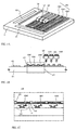
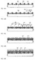
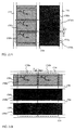
- Figs. 1A to 1C are diagrams for explaining the concept of the present invention.
- Fig. 1A shows a structure in which a pixel portion 102, a scanning line side driver circuit 103, and a data line side driver circuit 104 are formed on a substrate 101.
- Separation layers 105 are formed so as to form stripes in the pixel portion 102, and EL layers are formed between each separation layer.
- the separation layers 105 are formed in order that adjacent EL layers do not mutually mix when forming the EL layers by an ink-jet method.
- EL layers 106 are formed by discharging a liquid containing an EL material from an ink head 107.
- EL layer materials There are no particular limitations on EL layer materials, but to perform color display EL layers 106R, 106G, and 106B may be formed corresponding to red, green, and blue, respectively.
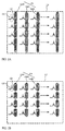
- Figs. 2A and 2B are diagrams for explaining details of the formation of the EL layers in the pixel portion.
- a plurality of current control TFTs 122 and a plurality of pixel electrodes 123 for connecting to the current control TFTs are formed, corresponding to each pixel, and arranged in a matrix state in the pixel portion 120, and the state of an EL layer 121 formed so as to form stripes corresponding to a selected row or column of the pixel electrodes is shown.
- EL layers 121R, 121G, and 121B corresponding to red, green, and blue, respectively, may be formed as shown in the figure for performing color display.
- EL layers 124 may also be formed to have an oblong shape or a rectangular shape corresponding to current control TFTs 125 arranged in a matrix state in a pixel portion 120 and pixel electrodes 126 connected to the current control TFTs 125.
- EL layers 124R, 124G, and 124B are similarly formed as shown in the figure.
- Fig. 1B is a cross sectional diagram of the schematic diagram shown by Fig. 1A, and shows the state in which the scanning line side driver circuit 103 and the pixel portion 102 are formed on the substrate 101.
- the separation layers 105 are formed in the pixel portion 102, and the EL layers 106R, 106G, and 106B are formed between each separation layer.
- the ink head 107 is part of the ink-jet method, and ink dots 108R, 108G, and 108B corresponding to the colors red, green, and blue, respectively, are discharged corresponding to a control signal.
- the discharged ink dots 108R, 108G, and 108B adhere to the substrate, and function as EL layers after later being dried or fired. As shown in Figs.
- the present invention is characterized in that the ink dots are formed having a continuous stripe shape, or an oblong or a rectangular shape on the substrate.
- the ink head may be scanned in one direction for every row or column, and therefore the processing time for forming the EL layers can be reduced.
- Fig. 1C is a diagram for explaining the pixel portion in additional detail, and current control TFTs 110 and pixel electrodes 112 connected to the current control TFTs 110 are formed on the substrate, and the EL layers 106R, 106G, and 106B are formed between the separation layers 105 on each pixel electrode. It is also preferable to form insulating films 111 having a blocking effect against alkali metals between the pixel electrodes 112 and the current control TFTs 110.
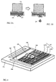
- Figs. 3A and 3B are diagrams for explaining the structure of the inkhead, and show an example in which the piezo method is used.
- Reference numeral 131 designates a piezo element (piezoelectric element); 132, a casing; and 133, an EL forming solution.
- the piezo element is deformed, and the casing 132 is also deformed.
- the EL forming solution 133 inside thereof is ejected as a droplet 134.
- the EL forming solution is carried out. In this case, since the EL forming solution 133 is pushed out by a physical external pressure, its composition etc. is not influenced at all.
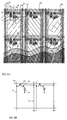
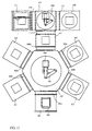
- Fig. 4 similarly is a diagram for explaining the concept of the present invention, and first separation layers 145 and second separation layers 146 formed orthogonal to the first separation layers 145 are formed in a pixel portion 142 formed on a substrate 141.
- EL layers 147 are formed in portions which are surrounded between the first separation layers 146 and the second separation layers 146.
- the first separation layers 145 and the second separation layers 146 are formed corresponding to each pixel electrode.
- the EL layers are formed by discharging an EL forming liquid containing an EL material from an ink head 148.
- EL layers 148R, 148G, and 148B may be formed corresponding to red, green, and blue, respectively, for performing color display.
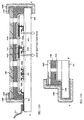
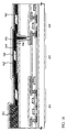
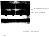
- FIG. 5 Shown in Fig. 5 is a cross sectional diagram of a pixel of the active matrix type EL display device of the present invention, and Fig. 6A is a top view, and Fig. 6B is a circuit structure of the active matrix type EL display device.
- a plurality of these types of pixels are arranged in a matrix state, forming a pixel portion (image display portion).
- FIG. 5 shows a cross section cut along the line A-A' in the top view shown in Fig. 6A.
- Common numerals are used in Fig. 5 and in Figs. 6A and 6B, and therefore the three figures may be referenced as appropriate.
- reference numeral 11 denotes a substrate
- reference numeral 12 denotes an insulating film serving as a base film.
- a glass substrate, a glass ceramic substrate, a quartz substrate, a silicon substrate, a ceramic substrate, a metallic substrate, or a plastic substrate (including a plastic film) can be used as the substrate 11.
- the base film 12 is especially effective for cases in which a substrate containing mobile ions, or a substrate having conductivity, is used, but need not be formed for a quartz substrate.
- An insulating film containing silicon may be formed as the base film 12.
- the term "insulating film containing silicon” indicates, specifically, an insulating film such as a silicon oxide film, a silicon nitride film, or a silicon nitride oxide film (denoted by SiOxNy) containing silicon, oxygen, and nitrogen in predetermined ratios.
- the base film 12 possess a heat radiating effect, it is also effective in preventing degradation of the TFTs and deterioration of EL elements due to the emission of heat generated by the TFTs.
- an alloy material containing Al such as an aluminum (Al) oxide or nitride, may also be formed.
- Reference numeral 201 denotes a TFT functioning as a switching element (hereafter referred to as a switching TFT), and reference numeral 202 denotes a TFT functioning as an current control element for controlling the amount of current flowing to the EL elements (hereafter referred to as a current control TFT). Both are formed from n-channel TFTs.
- TFT and the current control TFT are not necessary to limit the switching TFT and the current control TFT to n-channel TFTs, and that it is possible to use p-channel TFTs for either the switching TFT or the current control TFT, or for both. In any cases, selection of TFT type is made based on polarity of bias voltage applied to the EL element that is connected to the current control TFT.
- the switching TFT 201 is formed having: an active layer containing a source region 13, a drain region 14, LDD regions 15a to 15d, a high concentration impurity region 16, and channel forming regions 17a and 17b; a gate insulating film 18; gate electrodes 19a and 19b, a first interlayer insulating film 20, a source wiring 21, and a drain wiring 22.
- the gate electrodes 19a and 19b may be a double gate structure electrically connected by a gate wiring which is formed from a different material (a material having a lower resistance than the gate electrodes 19a and 19b). With this configuration, the device can deal with enlarged display size.
- a so-called multi-gate structure a structure containing an active layer having two or more channel forming regions connected in series
- a triple gate structure may also be used.
- the multi-gate structure is extremely effective in lowering the value of the off current, and by making the switching element 201 of the pixel into a multi-gate structure with the present invention, a low off current value can be realized for the switching element.
- the active layer is formed from a semiconductor film containing a crystal structure.
- a single crystal semiconductor film may be used, and a polycrystalline semiconductor film or a microcrystalline semiconductor film may also be used.
- the gate insulating film 18 may be formed from an insulating film containing silicon. Additionally, known wiring materials represented by Al. tantalum (Ta), tungsten (w), and the like can be used for the gate electrodes, the source wiring, and the drain wiring.
- the LDD regions 15a to 15d in the switching TFT 201 are formed sandwiching the gate insulating film 18, and so as not to overlay with the gate electrodes 17a and 17b. This structure is extremely effective in reducing the off current value.
- an offset region (a region having the same composition as the channel forming regions, and to which a gate voltage is not applied) between the channel forming regions and the LDD regions is more preferable for reducing the off current value.
- the high concentration impurity region formed between the channel forming regions is effective in lowering the value of the off current.
- the multi-gate structure TFT as the switching element 201, as above, a switching element having a sufficiently low off current value is realized by the present invention.
- the gate voltage of the current control TFT can therefore be maintained for a sufficient amount of time (for a period from one selection until the next selection) without forming a capacitor, such as the one illustrated in Fig. 2 in Japanese Patent Application Laid-open No. Hei 10-189252.
- the current control TFT 202 is formed having an active layer containing: a source region 31, a drain region 32, an LDD region 33, and a channel forming region 34; a gate insulating film 18; a gate electrode 35; a first interlayer insulating film 20; a source wiring 36; and a drain wiring 37.
- the gate electrode 35 has a single gate structure, but may also have a multi-gate structure.
- the drain of the switching TFT is electrically connected to the gate of the current control TFT.
- the gate electrode 35 of the current control TFT 202 is electrically connected to the drain region 14 of the switching TFT 201 through the drain wiring (also referred to as a connection wiring) 22.
- the source wiring 36 is connected to an current supply wiring 212.
- a characteristic of the current control TFT 202 is that its channel width is larger than the channel width of the switching TFT 201. Namely, as shown in Fig. 12, when the channel length of the switching TFT is taken as L1 and its channel width as W1, and the channel length of the current control TFT is taken as L2 and its channel width as W2, a relational expression is reached in which W2 / L2 ⁇ 5 x W1 / L1 (preferably W2 / L2 ⁇ 10 x W1 / L1 ). Consequently, it is possible for more current to easily flow in the current control TFT than in the switching TFT.
- the channel length L1 of the multi-gate structure switching TFT 201 is the sum of each of the channel lengths of the two or more channel forming regions formed.
- a double gate structure is formed in the case of Fig. 12, and therefore the sum of the channel lengths L1a and L1b, respectively, of the two channel-forming regions becomes the channel length L1 of the switching TFT 201.
- the channel lengths L1 and L2, and the channel widths W1 and W2 are not specifically limited to a range of values with the present invention, but it is preferable that W1 be from 0.1 to 5 ⁇ m (typically between 1 and 3 ⁇ m), and that W2 be from 0.5 to 30 ⁇ m (typically between 2 and 10 ⁇ m). It is preferable that L1 be from 0.2 to 18 ⁇ m (typically between 2 and 15 ⁇ m), and that L2 be from 0.1 to 50 ⁇ m (typically between 1 and 20 ⁇ m) at this time.
- the channel length L somewhat long in order to prevent excess current from flowing in the current control TFT 202. It may preferably be set such that W2 / L2 ⁇ 3 (more preferably W2 / L2 ⁇ 5 ). It is preferable that the amount of current flow per pixel is from 0.5 to 2 ⁇ A (more preferably, from 1 to 1.5 ⁇ A).
- the length (width) of the LDD region formed in the switching TFT 201 is set from 0.5 to 3.5 ⁇ m, typically between 2.0 and 2.5 ⁇ m.
- the EL display device shown in Fig. 5 is characterized in that, in the current control TFT 202, the LDD region 33 is formed between the drain region 32 and the channel forming region 34, and in that the LDD region 33 has a region which overlaps the gate electrode 35 through the gate insulating film 18, and a region which does not overlap the gate insulating film 18.
- the current control TFT 202 at the same time as supplying current for emitting light from an EL element 204, is capable of controlling the amount of current supplied, performing gradation display. Therefore, it is necessary to devise a countermeasure against deterioration due to hot carrier injection so that the TFT does not degrade even if a large current flows. Furthermore, the current control TFT 202 is set to an off state when displaying the color black, and if the value of the off current is high at that time, then the color black cannot be displayed clearly, leading to lowered contrast. It is therefore also necessary to control the value of the off current.
- the length of the LDD region which overlaps the gate electrode may be set from 0.1 to 3 ⁇ m (preferably between 0.3 and 1.5 ⁇ m) at this point. Too long and the parasitic capacity will become large; too short and the hot carrier prevention effect will become weak. Further, the length of the LDD region which does not overlap the gate electrode may be set from 1.0 to 3.5 ⁇ m (preferably between 1.5 and 2.0 ⁇ m). If it is too long, then sufficient current cannot flow, while if it is too short, then the effect of reducing the value of the off current will weaken.
- a parasitic capacitance is formed in the region in which the gate electrode and the LDD region overlap in the above structure, and therefore it is preferable to form this between the source region 31 and the channel forming region 34.
- the current control TFT always has the identical carrier (electron here) flow direction, and therefore it is sufficient to form the LDD region in only the drain region side.
- the film thickness of the active layer (in particular, the channel forming region) of the current control TFT 202 thicker (preferably from 50 to 100 nm, even better from 60 to 80 nm).
- the film thickness of the active layer (in particular, the channel forming region) thinner (preferably from 20 to 50 nm, even better between 25 and 40 nm).
- the film thickness of a first passivation film 41 may be set from 10 nm to 1 ⁇ m (preferably between 200 and 500 nm).
- An insulating film containing silicon in particular, a silicon nitride oxide film or a silicon nitride film is preferable
- the first passivation film 41 possesses a role of protecting the formed TFT from alkali metals and from moisture. Alkali metals such as sodium are contained in the EL layer to be formed later above the TFT. In other words, the first passivation film 41 works as a protecting layer so that alkali metals (mobile ions) do not ingress upon the TFT side.
- the first passivation film 41 possess a heat radiating effect, it is effective in preventing thermal degradation of the EL layer. Note that in order for light to be emitted from the substrate 11 side in an EL display device with the structure of Fig. 5, it is necessary for the first passivation film 41 to have light transmitting characteristics. In addition, when using an organic material as the EL layer, there is deterioration due to bonding with oxygen, and therefore it is preferable not to use an insulating film through which oxygen is easily released.
- An insulating film containing at least one element selected from the group consisting of B (boron), C (carbon), and N (nitrogen), and containing at least one element selected from the group consisting of Al (aluminum), Si (silicon), and P (phosphorous) can be given as a light transmitting material which prevents transmission of alkali metals and which additionally possesses a heat radiating effect.
- a nitride compound of aluminum typically aluminum nitride (Al x N y ), a carbide compound of silicon, typically silicon carbide (Si x C y ), a nitride compound of silicon, typically silicon nitride (Si x N y ), a nitride compound of boron, typically boron nitride (B x N y ), and a phosphide of boron, typically boron phosphide (B x P y ).
- an oxide of aluminum typically aluminum oxide (Al x O y )
- Al x O y has superior light transmitting characteristics, and a thermal conductivity of 20 Wm -1 K -1 , and is one of the preferable materials.
- these materials are also effective in preventing the incursion of moisture.
- nitrided aluminum oxide denoted by AlN x O y .
- This material in addition to a heat radiating effect, is also effective in preventing the incursion of moisture, alkali metals, and the like.
- an insulating film containing Si, Al, N, O, and M (where M denotes at least one rare earth element, preferably at least one element selected from the group consisting of Ce (cerium), Yb (ytterbium), Sm (samarium), Er (erbium), Y (yttrium), La (lanthanum), Gd (gadolinium), Dy (dysprosium), and Nd (neodymium)) can be used. These materials are also effective in preventing the incursion of moisture, alkali metals and the like, in addition to having a heat radiating effect.
- a carbon film containing at least a diamond thin film or an amorphous carbon film (in particular, one having characteristics close to those of diamond, referred to as diamond like carbon) can be used. These have extremely high thermal conductivities and are highly effective as heat radiating layers. Note that if the film thickness becomes thick, then it becomes brownish and the transmittivity is reduced, and therefore it is preferable to use as thin a film thickness as possible (preferably from 5 to 100 nm).
- the aim of the first passivation film 41 is to protect the TFTs from alkali metals and moisture, and therefore the material must not lose that effect. Therefore, a thin film made from the above materials which possess the heat radiating effect can be used alone, but it is effective to laminate these thin films with an insulating film which can prevent the transmission of alkali metals and moisture (typically a silicon nitride film (Si x N y ) or a silicon nitride oxide film (SiO x N y )).
- an insulating film typically a silicon nitride film (Si x N y ) or a silicon nitride oxide film (SiO x N y )
- Known materials may be employed for the EL layers of each color of pixel. Note that it is possible to implement the present invention without considering the method of light emission, and all four of the above methods can be used in the present invention.
- a second interlayer insulating film (which may also be referred to as a leveling film) 44 is formed having a shape which covers each of the TFTs, performing leveling of steps which arise due to the TFTs.
- An organic resin film is preferable as the second interlayer insulating film 44, and materials such as polyimide, polyamide, acrylic, and BCB (benzocyclobutene) may be used.
- An inorganic film may also be used, of course, provided that it is capable of sufficient leveling.
- the leveling of the steps due to the TFTs by the second interlayer insulating film 44 is extremely important.
- the EL layers formed later are extremely thin, and therefore there are cases of cracks and short circuits between anodes and cathodes in portions in which the step exists. It is therefore preferable to perform leveling before forming pixel electrodes in order to be able to form the EL layers on as level a surface as possible.
- a second passivation film 45 shoulders a vital role of blocking the diffusion of alkali metals from the EL elements. Its film thickness may be set from 5 nm to 1 ⁇ m (typically between 20 and 300 nm). An insulating film which can prevent the transmission of alkali metals is used in the second passivation film 45.
- the materials used as the first passivation film 41 can also be used as the materials for the second passivation film 45.
- the second passivation film 45 also functions as a heat radiating layer and releases heat generated by the EL elements so that heat does not accumulate in the EL elements.
- the second passivation film 45 ensures that heat generated by the EL elements does not impart any bad influence to the second interlayer insulating film 44.
- the second passivation film 45 also functions as a protecting layer for ensuring that alkali metals within the EL layers do not diffuse to the TFT side, and moreover, also functions as a protecting layer to ensure that moisture and oxygen from the TFT side do not penetrate to the EL layer side.
- a pixel electrode (anode of EL element) 46 is a transparent conductive film, and after opening a contact hole in the second passivation film 45, in the second interlayer insulating film 44, and in the first passivation film 41, the pixel electrode 46 is formed so as to connect to the drain wiring 37 of the current control TFT 202 in the formed contact hole portion.
- a separation layer 101 is formed from an organic resin film on the second passivation film 45.
- the separation layer 101 is formed by a spin coating method from a photosensitive polyimide film, and a separation layer 101 is formed by patterning.
- the separation layer 101 has a shape as when forming the EL layers by an ink-jet method, and the EL element formation locations can be demarcated by the placement of the separation layer.
- an EL layer (preferably an organic material) 47 is formed by an ink-jet method.
- a single layer structure or a lamination structure can be used for the EL layer 47, and there are many cases of using a lamination structure.
- Various lamination structures have been proposed in which layers such as a light emitting layer, an electron transporting layer, an electron injecting layer, a hole injecting layer, and a hole transporting layer are combined, and any structure may be used for the present invention. Further, a fluorescent pigment or the like may also be doped into the EL layer.
- Organic materials are widely known as such materials, and considering the driver voltage, it is preferable to use an organic material.
- the materials disclosed in the following U.S. Patents and Japanese patent applications can be used as the organic EL material:
- an organic material such as the one shown by the following general formula can be used as a hole injecting layer.
- Q is either N or a C-R (carbon chain);
- M is a metal, a metal oxide compound, or a metal halogen compound;
- R is hydrogen, an alkyl, an aralkyl, an allyl, or an alkalyl; and
- T1 and T2 are unsaturated six-membered ring including substituents such as hydrogen, alkyls, or halogens.
- an aromatic tertiary amine can be used as an organic material hole transporting layer, preferably including the tetra-allyl-diamine shown by the following general formula.
- Chem 2 are an allylene group, n is an integer from 1 to 4, and AR, R 7 , R 8 , and R 9 are each chosen allyl group.
- a metal oxynoid compound can be used as an organic material EL layer, electron transporting layer, or electron injecting layer.
- a material such as that shown by the general formula below may be used as the metal oxynoid compound.
- R 2 through R 7 It is possible to substitute R 2 through R 7 , and a metal oxynoid compound such as the following can also be used.
- R 2 through R 7 are defined as stated above; L 1 through L 5 are carbohydrate groups containing from 1 to 12 carbon elements; and both L 1 and L 2 , or both L 2 and L 3 are formed from benzo-rings. Further, a metal oxynoid compound such as the following may also be used.
- the present invention uses an ink jet method in forming the EL layer, and hence it is preferable to use a polymer-based material as the EL material.
- a polymer material such as polyparaphenylene vinylenes (PPVs) type material and polyfluorenes type material can be given as typical polymer-based materials.
- PSVs polyparaphenylene vinylenes
- the ink-jet method is roughly divided into a bubble jet method (also referred to as a thermal ink-jet method) and a piezo method, and that the piezo method is preferable for implementing the present invention.
- the shape at the time of applying the EL material on the pixel electrodes may be a strip shape, or an oblong shape or a rectangular shape in which a plurality of dots are continuous.
- the separation layer 101 functions so that adjacent EL layers do not mutually intermix when the EL layers are formed by the ink-jet method.
- a red color light emitting EL layer 47R, a green color light emitting layer 47G, and a blue color light emitting EL layer 47B are formed as shown in Fig. 6A.
- the EL layers may each be formed in order at this point, and the EL layers corresponding respectively to red, green, and blue may be formed at the same time.
- a baking (firing) process is necessary in order to remove a solvent contained in the EL forming solution.
- the baking process may be performed after forming all of the EL layers. Alternatively, it may be performed every time the formation of one EL layer is completed.
- the EL layer is thus formed to have a thickness of from 50 to 250 nm.
- Figs. 21A and 21B are diagrams for explaining the structure in the pixel portion, and show a state in which a plurality of pixel electrodes are formed in EL layers formed having a stripe shape, or an oblong shape or rectangular shape.
- a plurality of pixel electrodes are formed corresponding to the different color light emitting EL layers 1702a and 1702b in Fig. 21A.
- Two TFTs, a switching TFT and an current control TFT, are connected to each of the pixel electrodes.
- the EL layer 1702a and the EL layer 1702b are separated by a separation layer 1701.
- pixel electrodes 1703a and 1703b are taken as one set, forming one pixel 1710a.
- the value of D is set from 5 to 10 times the thickness of the EL layers. Namely, it is set from 250 to 2500 nm.
- Fig. 21B is a diagram showing an example of another structure.
- a plurality of pixel electrodes are formed corresponding to different color light emitting EL layers 1705a, 1705b, and 1705c, for example red, green, and blue.
- the EL layers are separated by separation layers 1704.
- the pixel electrodes 1706a, 1706b, and 1706c are taken as one set, forming one pixel 1720a.
- An adjacent pixel 1710b is formed similarly, and taking the gap between pixels as D, the value of D is set to be from 5 to 10 times the thickness of the EL layers. Namely, it is set from 250 to 2500 nm. A sharp image display can thus be made.
- the EL layer 47 when forming the EL layer 47, it is preferable to use a dry atmosphere having as little moisture as possible as the processing environment, and it is preferable to performing the formation within an inert gas.
- the EL layer easily deteriorates due to the existence of moisture and oxygen, and therefore it is necessary to eliminate these causes as much as possible when forming the EL layer 47.
- atmospheres such as a dry nitrogen atmosphere and a dry argon atmosphere are preferable.
- a cathode 48 and an auxiliary electrode 49 are formed next.
- a light emitting element formed from the pixel electrode (anode), the EL layer, and the cathode is referred to as an EL element throughout this specification.
- An MgAgAl electrode, an LiAl electrode, and an LiFAl electrode can be given as other examples.
- the auxiliary electrode 49 is an electrode formed in order to be a protecting film from external moisture or the like, and a material containing aluminum (Al) or silver (Ag) is used.
- the auxiliary electrode 48 also has a heat radiating effect.
- the EL layer 47 and the cathode 48 are formed successively in a dry, inert atmosphere without exposure to the atmosphere. This is in order to avoid the absorption of moisture during exposure to the atmosphere because an organic material, when used as the EL layer, is extremely weak to moisture. In addition, it is even better to form not only the EL layer 47, the cathode 48, but also the auxiliary electrode 49 in succession.
- a third passivation film 50 may have a film thickness from 10 nm to 1 ⁇ m (preferably between 200 and 500 nm).
- the aim of forming the third passivation film 50 is mainly for protecting the EL layer 47 from moisture, and it may also be given a heat radiating effect similar to the second passivation film 45.
- the same materials as those used in the first passivation film 41 can therefore be used as the formation material of the third passivation film 50. Note that when an organic material is used as the EL layer 47, there is the possibility of deterioration due to bonding with oxygen, and therefore it is preferable to use an insulating film through which oxygen is easily radiated.
- the EL layer is weak with respect to heat, as stated above, and therefore it is preferable to perform film deposition at as low a temperature as possible (preferably in a temperature range from room temperature to 120°C). It can therefore be said that plasma CVD, sputtering, vacuum evaporation, ion plating, and solution application (spin coating) are preferable film deposition methods.
- Deterioration of the EL element can be sufficiently controlled by forming only the second passivation film 45, but it is more preferable to surround the EL element by sandwiching it using two insulating films, the second passivation film 45 and the third passivation film 50, thus preventing incursion of moisture and oxygen into the EL layer, stopping diffusion of alkali metals from the EL layer, and preventing accumulation of heat in the EL layer. As a result, deterioration of the EL layer is additionally suppressed, and an EL display device having high reliability can be obtained.
- the EL display device of the present invention has the pixel portion composed of pixels having the structure shown in Fig. 5, and TFTs having differing structures, corresponding to their function, are arranged within the pixels.
- a switching TFT having a sufficiently low off current value, and an current control TFT which is strong against hot carrier injection can thus be formed within the same pixel, and an EL display device having high reliability and good image display capabilities (high operation performance) can be obtained.
- a multi-gate structure TFT is used as the switching TFT in the pixel structure of Fig. 5, but it is not necessary to limit the structure to that of Fig. 5 with regard to LDD region placement and other structures.
- a more detailed explanation of the present invention having the above constitution is performed by the embodiments shown below.
- CMOS circuit is shown as a basic circuit for the driver circuits.
- a base film 301 is formed with a 300 nm thickness on a glass substrate 300.
- Silicon nitride oxide films are laminated as the base film 302 in embodiment 1. It is good to set the nitrogen concentration at between 10 and 25 wt% in the film contacting the glass substrate 300.
- the base film 301 it is effective to provide an insulating film made of a material similar to the first passivation film 41 shown in Fig. 5.
- the current controlling TFT is apt to generate heat since a large current is made to flow, and it is effective to provide an insulating film having a heat radiating effect at a place as close as possible.
- an amorphous silicon film (not shown in the figures) is formed with a thickness of 50 nm on the base film 301 by a known deposition method. Note that it is not necessary to limit this to the amorphous silicon film, and another film may be formed provided that it is a semiconductor film containing an amorphous structure (including a microcrystalline semiconductor film). In addition, a compound semiconductor film containing an amorphous structure, such as an amorphous silicon germanium film, may also be used. Further, the film thickness may be made from 20 to 100 nm.
- the amorphous silicon film is then crystallized by a known method, forming a crystalline silicon film (also referred to as a polycrystalline silicon film or a polysilicon film) 302.
- a crystalline silicon film also referred to as a polycrystalline silicon film or a polysilicon film
- Thermal crystallization using an electric furnace, laser annealing crystallization using a laser, and lamp annealing crystallization using an infrared lamp exist as known crystallization methods. Crystallization is performed in embodiment 1 by laser annealing using light from an excimer laser which uses XeCl gas.
- pulse emission type excimer laser light formed into a linear shape is used in embodiment 1, but a rectangular shape may also be used, and continuous emission argon laser light and continuous emission excimer laser light can also be used.
- the light source of laser is not limited to excimer laser, the second harmonic or the third harmonic of YAG laser can be used.
- the crystalline silicon film is used as the active layer of the TFT, it is also possible to use an amorphous silicon film.
- the current control TFT has necessity of flowing a mass current, it is advantageous to use the crystalline silicon film through which a current can easily flow.
- a protecting film 303 is formed on the crystalline silicon film 302 with a silicon oxide film having a thickness 0 130 nm. This thickness may be chosen within the range of 100 to 200 nm (preferably between 130 and 170 nm). Furthermore, other films may also be used providing that they are insulating films containing silicon.
- the protecting film 303 is formed so that the crystalline silicon film is not directly exposed to plasma during addition of an impurity, and so that it is possible to have delicate concentration control of the impurity.
- Resist masks 304a and 304b are then formed on the protecting film 303, and an impurity element which imparts n-type conductivity (hereafter referred to as an n-type impurity element) is added.
- an impurity element which imparts n-type conductivity hereafter referred to as an n-type impurity element
- elements residing in periodic table group 15 are generally used as the n-type impurity element, and typically phosphorous or arsenic can be used.
- a plasma doping method is used, in which phosphine (PH 3 ) is plasma activated without separation of mass, and phosphorous is added at a concentration of1x10 18 atoms/cm 3 in embodiment 1.
- An ion implantation method, in which separation of mass is performed, may also be used, of course.
- the dose amount is regulated so that the n-type impurity element is contained in n-type impurity regions 305 and 306, thus formed by this process, at a concentration of 2x10 16 to 5x10 19 atoms/cm 3 (typically between 5x10 17 and 5x10 18 atoms/cm 3 ).
- the protecting film 303 is removed, and an activation of the added periodic table group 15 elements is performed.
- a known technique of activation may be used as the means of activation, and activation is done in embodiment 1 by irradiation of excimer laser light.
- a pulse emission type excimer laser and a continuous emission type excimer laser may both, of course, be used, and it is not necessary to place any limits on the use of excimer laser light.
- the purpose is the activation of the added impurity element, and it is preferable that irradiation is performed at an energy level at which the crystalline silicon film does not melt. Note chat the laser irradiation may also be performed with the protecting film 303 in place.
- the activation by heat treatment may also be performed along with activation of the impurity element by laser light. When activation is performed by heat treatment, considering the heat resistance of the substrate, it is good to perform heat treatment on the order of 450 to 550 °C.
- a boundary portion (connecting portion) with regions along the edges of the n-type impurity regions 305 and 306, namely regions along the perimeter into which the n-type impurity element, which exists in the n-type impurity regions 305 and 306, is not added, is delineated by this process. This means that, at the point when the TFTs are later completed, extremely good connections can be formed between LDD regions and channel forming regions.
- a gate insulating film 311 is formed, covering the active layers 307 to 310.
- a single layer structure or a lamination structure may be used.
- a 110 nm thick silicon nitride oxide film is used in embodiment 1.
- gate electrodes 312 to 316 A conducting film with a thickness of 200 to 400 nm is formed next and patterned, forming gate electrodes 312 to 316.
- the gate electrodes and lead wirings electrically connected to the gate electrodes are formed from different materials. Specifically, a material having a lower resistance than that of the gate electrodes is used for the gate wirings. This is because a material which is capable of being micro-processed is used as the gate electrodes, and even if the gate wirings cannot be micro-processed, the material used for the wirings has low resistance.
- the gate electrodes and the gate wirings may also be formed from the same material.
- the gate wirings may be formed by a single layer conducting film, and when necessary, it is preferable to use a two layer or a three layer lamination film. All known conducting films can be used as the gate electrode material. However, as stated above, it is preferable to use a material which is capable of being micro-processed, specifically, a material which is capable of being patterned to a line width of 2 ⁇ m or less.
- the films may be used as a single layer or a laminate layer.
- a laminate film of a tantalum nitride (TaN) film having a thickness of 50 nm and a Ta film having a thickness of 350 nm is used. These may be formed by a sputtering method. When an inert gas of Xe, Ne or the like is added as a sputtering gas, film peeling due to stress can be prevented.
- TaN tantalum nitride
- the gate electrodes 313 and 316 are formed at this time so as to overlap a portion of the n-type impurity regions 305 and 306, respectively, sandwiching the gate insulating film 311. This overlapping portion later becomes an LDD region overlapping the gate electrode.
- an n-type impurity element (phosphorous is used in embodiment 1) is added in a self-aligning manner with the gate electrodes 312 to 316 as masks, as shown in Fig. 8A.
- the addition is regulated so that phosphorous is added to impurity regions 317 to 323 thus formed at a concentration of 1/10 to 1/2 that of the impurity regions 305 and 306 (typically between 1/4 and 1/3).
- a concentration of 1x10 16 to 5x10 18 atoms/cm 3 (typically 3x10 17 to 3x10 18 atoms/cm 3 ) is preferable.
- Resist masks 324a to 324c are formed next, with a shape covering the gate electrodes etc, as shown in Fig. 8B, and an n-type impurity element (phosphorous is used in embodiment 1) is added, forming impurity regions 325 to 331 containing a high concentration of phosphorous.
- Ion doping using phosphine (PH 3 ) is also performed here, and is regulated so that the phosphorous concentration of these regions is from 1x10 20 to 1x10 21 atoms/cm 3 (typically between 2x10 20 and 5x10 21 atoms/cm 3 ).
- a source region or a drain region of the n-channel TFT is formed by this process, and in the switching TFT, a portion of the n-type impurity regions 320 to 322 formed by the process of Fig. 8A remains. These remaining regions correspond to the LDD regions 15a to 15d of the switching TFT in Fig. 5.
- the resist masks 324a to 324c are removed, and a new resist mask 332 is formed.
- a p-type impurity element (boron is used in embodiment 1) is then added, forming impurity regions 333 and 334 containing a high concentration of boron. Boron is added here to form impurity regions 333 and 334 at a concentration of 3x10 20 to 3x10 21 atoms/cm 3 (typically between 5x10 20 and 1x10 21 atoms/cm 3 ) by ion doping using diborane (B 2 H 6 ).
- phosphorous has already been added to the impurity regions 333 and 334 at a concentration of 1x10 20 to 1x10 21 atoms/cm 3 , but boron is added here at a concentration of at least 3 times than of the phosphorous. Therefore, the n-type impurity regions already formed completely invert to p-type, and function as p-type impurity regions.
- the n-type and p-type impurity elements added at various concentrations are activated.
- Furnace annealing, laser annealing, or lamp annealing may be performed as a means of activation.
- Heat treatment is performed in embodiment 1 in a nitrogen atmosphere for 4 hours at 550°C in an electric furnace.
- the concentration of oxygen in the processing environment in the above activation process should be 1 ppm or less, desirably 0.1 ppm or less.
- a gate wiring 335 with a thickness of 300 nm is formed next as shown in Fig. 8D.
- a metallic film having aluminum (Al) or copper (Cu) as its principal constituent (comprising 50 to 100% of the composition) may be used as the material of the gate wiring 335.
- the gate wiring 335 is formed with a placement so that the gate electrodes 314 and 315 of the switching TFTs (corresponding to gate electrodes 19a and 19b of Fig. 2) are electrically connected.
- the wiring resistance of the gate wiring can be made extremely small by using this type of structure, and therefore a pixel display region (pixel portion) having a large surface area can be formed.
- the pixel structure of embodiment 1 is extremely effective because an EL display device having a screen size of a 10 inch diagonal or larger (in addition, a 30 inch or larger diagonal) is realized due to this structure.
- a first interlayer insulating film 336 is formed next, as shown in Fig. 9A.
- a single layer insulating film containing silicon is used as the first interlayer insulating film 336, while a lamination film may be combined in between. Further, a film thickness of between 400 nm and 1.5 ⁇ m may be used.
- a lamination structure of an 800 nm thick silicon oxide film on a 200 nm thick silicon nitride oxide film is used in embodiment 1.
- heat treatment is performed for 1 to 12 hours at 300 to 450° C in an environment containing between 3 and 100% hydrogen, performing hydrogenation.
- This process is one of hydrogen termination of dangling bonds in the semiconductor film by hydrogen which is thermally activated.
- Plasma hydrogenation (using hydrogen activated by a plasma) may also be performed as another means of hydrogenation.
- the hydrogenation step may also be inserted during the formation of the first interlayer insulating film 336. Namely, hydrogen processing may be performed as above after forming the 200 nm thick silicon nitride oxide film, and then the remaining 800 nm thick silicon oxide film may be formed.
- this electrode is made of a laminate film of three-layer structure in which a titanium film having a thickness of 100 nm, an aluminum film containing titanium and having a thickness of 300 nm, and a titanium film having a thickness of 150 nm are continuously formed by a sputtering method.
- a titanium film having a thickness of 100 nm, an aluminum film containing titanium and having a thickness of 300 nm, and a titanium film having a thickness of 150 nm are continuously formed by a sputtering method.
- other conductive films may be used.
- a first passivation film 344 is formed next with a thickness of 50 to 500 nm (typically between 200 and 300 nm).
- a 300 nm thick silicon nitride oxide film is used as the first passivation film 344 in embodiment 1. This may also be substituted by a silicon nitride film. It is of course possible to use the same materials as those of the first passivation film 41 of Fig. 5.
- a second interlayer insulating film 347 made of organic resin is formed.
- the organic resin it is possible to use polyimide, polyamide, acryl, BCB (benzocyclobutene) or the like.
- the second interlayer insulating film 346 is primarily used for flattening, acryl excellent in flattening properties is preferable.
- an acrylic film is formed to a thickness sufficient to flatten a stepped portion formed by TFTs. It is appropriate that the thickness is preferably made 1 to 5 ⁇ m (more preferably, 2 to 4 ⁇ m).
- a second passivation film 348 having a thickness of 100 nm is formed on the second interlayer insulating film 347.
- an insulating film containing Si, Al, N, O and La is used, it is possible to prevent alkaline metal from diffusing from the EL layer provided thereon. At the same time, intrusion of moisture into the EL layer is blocked and heat generated in the EL layer is dissipated, so that it is possible to suppress deterioration of the EL layer due to heat and deterioration of the flattened film (second interlayer insulating film).
- a contact hole reaching a drain wiring 343 is formed through the second passivation film 348, the second interlayer insulating film 347, and the first passivation film 344, and a pixel electrode 349 is formed.
- an indium-tin oxide (ITO) film having a thickness of 110 nm is formed, and patterning is carried out to form the pixel electrode.
- This pixel electrode 349 becomes an anode of the EL element.
- ITO indium-tin oxide
- this embodiment has such a structure that the pixel electrode 349 is electrically connected to the drain region 331 of the current controlling TFT through the drain wiring 343.
- This structure has merits as follows:
- the pixel electrode 349 comes in direct contact with an organic material of an EL layer (light emitting layer) or charge transporting layer, there is a possibility that a movable ion contained in the EL layer or the like diffuses in the pixel electrode. That is, in the structure of this embodiment, the pixel electrode 349 is not directly connected to the drain region 331 as a part of the active layer, but the drain wiring 343 is made to intervene so that intrusion of the movable ion into the active layer can be prevented.
- an EL layer 350 is formed by an ink jet method, and further, a cathode (MgAg electrode) 351 and a protecting electrode 352 are formed without opening to the air. At this time, it is desirable to completely remove moisture by carrying out a heat treatment to the pixel electrode 349 before the EL layer 350 and the cathode 351 are formed.
- MgAg electrode is used as the cathode of the EL element, other well-known materials may be used.
- the materials explained in the embodiment mode 2 of the invention can be used.
- a four-layer structure of a hole injecting layer, a hole transporting layer, a light emitting layer and an electron transporting layer are made an EL layer, there is also a case where an electron transporting layer is not formed, where an electron injecting layer is provided, or where a hole injecting layer is omitted.
- various examples have already been reported for the combination, and any structure of them may be used.
- An amine such as TPD may be used as the hole injecting layer or as the hole transporting layer, and in addition, a hydrazone (typically DEH), a stilbene (typically STB), or a starburst (typically m-MTDATA) can also be used.
- a starburst material which has a high glass transition temperature and is difficult to crystallize, is preferable.
- BPPC, perylene, and DCM can be used as a red color emitting layer in the emitting layer, and in particular, the Eu complex shown by Eu(DBM) 3 (Phen) (refer to Kido, J., et. al, Appl. Phys., vol. 35, pp. L394-396, 1996 for details) is highly monochromatic, possessing a sharp emission at a wavelength of 620 nm.
- an Alq 3 (8-hydroxyquinoline aluminum) material in which quinacridone or coumarin is added at a level of several mol% can be used as a green color emitting layer.
- a distile-arylene amino dielectric in which amino substituted DSA is added to DSA (distile-arylene dielectric) can be used as a blue color emitting layer.
- distilyl-biphenyl DPVBi
- DPVBi high performance material distilyl-biphenyl
- a third passivation film 353 may be provided.
- a silicon nitride film having a thickness of 300 nm is provided.
- This third passivation film may also be formed continuously after the auxiliary electrode 352 without opening to the air.
- the same material as the third passivation film 50 of Fig. 5 may be used.
- the auxiliary electrode 352 is provided to prevent deterioration of the MgAg electrode 351, and a metal film containing aluminum as its main ingredient is typical. Of course, another material may be used. Since the EL layer 350 and the MgAg electrode 351 are very weak to moisture, it is desirable to make continuous formation to the auxiliary electrode 352 without opening to the air so that the EL layer is protected from the outside air.
- the thickness of the EL layer 350 is made 10 to 400 nm (typically 60 to 160 nm), and the thickness of the MgAg electrode 351 is made 180 to 300 nm (typically 200 to 250 nm).
- the film thickness of each layer is the range of 10 to 100 nm.
- an active matrix type EL display device having a structure as shown in Fig. 9C is completed.
- a TFT having an optimum structure is disposed in not only the pixel portion but also the driving circuit portion, so that very high reliability is obtained and operation characteristics can also be improved.
- a TFT having a structure to decrease hot carrier injection so as not to drop the operation speed thereof as much as possible is used as an n-channel TFT 205 of a CMOS circuit forming a driving circuit.
- the driving circuit here includes a shift register, a buffer, a level shifter, a sampling circuit (sample and hold circuit) and the like.
- a signal conversion circuit such as a D/A converter can also be included.
- the active layer of the n-channel 205 includes a source region 355, a drain region 356, an LDD region 357 and a channel formation region 358, and the LDD region 357 overlaps with the gate electrode 313, putting the gate insulating film 311 therebetween.
- the LDD region 357 is made to completely overlap with the gate electrode to decrease a resistance component to a minimum. That is, it is preferable to remove the so-called offset.
- a TFT having a structure as shown in Fig. 13. As shown in Fig. 13, parts of LDD regions 901a and 901b overlap with a gate electrode 903, putting a gate insulating film 902 therebetween. This effect is as set forth in the explanation of the current controlling TFT 202, and a different point is that in the sampling circuit, the LDD regions 901a and 901b are provided to be put at both sides of a channel formation region 904.
- the pixel portion is formed by forming the pixel structure which is shown in the Fig. 5.
- the structure of the switching TFT or the current control TFT formed in a pixel is not provided an explanation because it was given in Fig. 5.
- a housing member such as a protection film having high airtightness and less degassing (laminate film, ultraviolet ray curing resin film, etc.) or a ceramic sealing can so as to prevent exposure to the outer air.
- a housing member such as a protection film having high airtightness and less degassing (laminate film, ultraviolet ray curing resin film, etc.) or a ceramic sealing can so as to prevent exposure to the outer air.
- a housing member such as a protection film having high airtightness and less degassing (laminate film, ultraviolet ray curing resin film, etc.) or a ceramic sealing can so as to prevent exposure to the outer air.
- a connector flexible print circuit: FPC
- FPC flexible print circuit
- the active matrix type EL display device of this embodiment is constituted by a pixel portion 602, a gate side driving circuit 603, and a source side driving circuit 604 formed on a glass substrate 601.
- a switching TFT 605 of a pixel portion is an n-channel TFT, and is disposed at an intersection point of a gate wiring 606 connected to the gate side driving circuit 603 and a source wiring 607 connected to the source side driving circuit 604.
- the drain of the switching TFT 605 is connected to the gate of a current controlling TFT 608.
- the source of the current controlling TFT 606 is connected to a current supply line 609.
- a current supply line 609 is given an earth electric potential.
- An EL element 610 is connected to the drain of the current controlling TFT 608. Further, a cathode of the EL element 610 is added a fixed voltage (10 to 12 V in this embodiment).
- Input-output wirings (connection wirings) 612 and 613 for transmitting signals to the driving circuits and an input-output wiring 614 connected to the current supply line 609 are provided in an FPC 611 as an external input-output terminal.
- circuit structure of the EL display device shown in Fig. 10 is shown in Fig. 11.
- the circuit structure shown in Fig. 11 is an example of an analog driving, a source side driving circuit 701, a gate side driving circuit (A) 707, a gate side driving circuit (B) 711, and a pixel portion 706.
- the term "driving circuit" is a general term including the source side driving circuit and the gate side driving circuit.
- the source side driving circuit 701 is provided with a shift register 702, a level shifter 703, a buffer 704, and a sampling circuit (sample and hold circuit) 705.
- the gate side driving circuit (A) 707 is provided with a shift register 708, a level shifter 709, and a buffer 710.
- the gate side driving circuit (B) 711 also has the same structure.
- the shift registers 702 and 708 have driving voltages of 5 to 16 V (typically 10 V) respectively, and the structure indicated by 205 in Fig. 9C is suitable for an n-channel TFT used in a CMOS circuit forming the circuit.
- the CMOS circuit including the n-channel TFT 205 of Fig. 9C is suitable for each of the level shifters 703 and 709 and the buffers 704 and 710, while the driving voltage is raised 14 to 16 V, similarly to the shift register.
- the CMOS circuit including the n-channel TFT 205 of Fig. 9C is suitable for each of the level shifters 703 and 709 and the buffers 704 and 710.
- it is effective to make a gate wiring a multi-gate structure such as a double gate structure or a triple gate structure in improvement of reliability of each circuit.
- a CMOS circuit including the n-channel TFT 208 of Fig. 13 is suitable for the sampling circuit 705 while its driving voltage is 14 to 16V.
- the pixel portion 706, which driving voltage is 14 to 16V, are disposed pixels having the structure shown in Fig. 5.
- the foregoing structure can be easily realized by manufacturing TFTs in accordance with the manufacturing steps shown in Figs. 7A to 9C.
- a logical circuit other than the driving circuit such as a signal dividing circuit, a D/A converter circuit, an operational amplifier circuit, a ⁇ correction circuit, or the like on the same substrate, and further, it is believed that a memory portion, a microprocessor, or the like can be formed.
- EL module of this embodiment including a housing member as well will be described with reference to Figs. 14, 15A and 15B. Incidently, as needed, reference numbers used in Figs. 10 and 11 will be quoted.
- reference numeral 601 denotes a substrate
- reference numeral 602 denotes a pixel portion
- 603 denotes a source side driver circuit
- 604 denotes a gate side driver circuit
- 612 denotes connection wirings for electrically connecting the pixel portion 602, the source side driver circuit 603, and the gate side driver circuit 604 to an FPC (flexible printed circuit) 611.
- the FPC is electrically connected to external equipment, and external signals can thus be input to the pixel portion 602, the source side driver circuit 603, and the gate side driver circuit 604.
- the pixel portion 602, the source side driver circuit 603, and the gate side driver circuit 604 are formed from thin film transistors (hereafter referred to as TFTs) formed on the substrate 601.
- TFTs having any type of structure may be used as the TFTs.
- Known structures may also be used, of course.
- a filler material (not shown in the figure), a covering material 1407, a sealing material (not shown in the figure), and a frame material 1408 are formed.
- FIG. 15A A cross sectional diagram of Fig. 14 cut along the line A-A is shown in Fig. 15A, and a cross sectional diagram of Fig. 14 cut along the line B-B is shown in Fig. 15B. Note that in Figs. 15A and 15B, identical numerals are used for portions identical to those of Fig. 14.
- the pixel portion 602 and the driver circuit 603 are formed on the substrate 601, and the pixel portion 602 is composed of a plurality of pixels containing an current control TFT 1501 and a pixel electrode 1502 electrically connected to the current control TFT 1501.
- the pixel electrode 1502 functions as an anode of an EL element.
- an EL layer 1503 is formed covering the pixel electrode 1502, and a cathode 1504 of the EL element is formed on the EL layer 1503.
- the cathode 1504 also functions as a common wiring among all pixels, and is electrically connected to the FPC 611 via the connection wirings 612.
- the element containing the pixel portion 602 and the driver circuit 603 is completely covered by a passivation film 1507.
- a filler material 1508 is formed covering the EL element.
- the filler material 1508 functions as an adhesive for bonding the covering material 1407.
- PVC polyvinyl chloride
- epoxy resin epoxy resin
- silicone resin silicone resin
- PVB polyvinyl butyral
- EVA ethylene vinyl acetate
- materials such as a glass plate, an aluminum plate, a stainless steel plate, an FRP (fiberglass-reinforced plastic) plate, a PVF (polyvinyl fluoride) film, a Mylar film, a polyester film, and an acrylic film can be used as the covering material 1407.
- PVB or EVA polyvinyl fluoride
- the covering material 1407 depending on the emission direction of light emitted from the EL element, it is necessary for the covering material 1407 to possess transparency. In other words, for the case of Figs. 15A and 15B, light is irradiated to the side opposite that of the covering material 1407, and therefore the material properties do not matter, but for a case in which the light is irradiated to the covering material 1407 side, a highly transparent material is used.
- the frame material 1408 is attached so as to cover the side surface (exposed surface) of the filler material 1508.
- the frame material 1408 is bonded by a sealing material (which functions as a sealant) 1509.
- a sealing material which functions as a sealant
- a photo curing resin as the sealing material 1509 at this point, but a thermally curable resin may also be used provided that the thermal resistance of the EL layer permits.
- the sealing material 1509 be a material through which as little moisture and oxygen as possible are transmitted. Further, a drying agent may also be added to the inside of the sealing material 1509.
- the EL element By sealing the EL element in the filler material 1508 using the above method, the EL element can be completely shut off from the outside, and the incursion of substances from the outside which promote degradation by oxidation of the EL layer through moisture, oxygen, etc. can be prevented. An EL display device having high reliability can therefore be manufactured.
- Embodiment 1 An EL display device having a form in which light emitted by an EL element is irradiated to the side of a substrate on which TFTs are formed is shown in Embodiment 1. For this case, at least the region in which the TFTs are formed becomes shadow, and the aperture ratio of a pixel portion is reduced by that amount. On the other hand, if a form is used in which light emitted by the EL element is irradiated in the upward direction (the side of the substrate opposite that on which the TFTs are formed), then at least it becomes easy to increase the aperture ratio.
- Fig. 18 shows the structure of an EL display element in which light is irradiated in the upward direction.
- the structures of the switching TFT 201 and the current control TFT 202 are the same as those of Embodiment Mode 2, and the differences in other portions is explained here.
- a cathode side pixel electrode 949 connected to the drain side of the current control TFT 202 is formed on a second passivation layer 945.
- a separation layer 951 is formed from an organic resin material.
- the EL layer 947 is also formed by an ink-jet method similar to that of Embodiment Mode 1 or Embodiment Mode 2.
- an anode side pixel electrode is formed from a transparent conducting material such as ITO, and a third passivation film 950 is formed on the anode side pixel electrode, completing the EL display element in which light is irradiated in the upward direction.
- the method of manufacturing an EL layer by an ink-jet method, and the manufactured EL layer according to the present invention, can also be applied to a passive type EL display device.
- An example of such is explained with reference to Figs. 16A to 16E.
- a substrate such as: a non-alkaline glass substrate, typically a Corning Corp. # 1737 glass substrate; a crystalline glass substrate; a soda lime glass substrate on whose surface a silicon oxide film or a silicon nitride film is formed; or a plastic substrate can be applied to a substrate 1601 in Fig. 16A.
- a transparent electrode 1602 is formed with a film thickness of 50 to 200 nm on the substrate 1601, and is partitioned into a plurality of strip shapes by a process such as etching or lift-off.
- the transparent electrode 1601 is formed from a material such as ITO, ZnO, SnO 2 , or ITO-ZnO.
- separating layers 1603 are formed with a thickness of 0.5 to 2 ⁇ m so as to contact the side edge portions of the transparent electrode 1602 formed into the strip shapes.
- the EL layer uses a single layer or a lamination structure.
- a lamination structure is a structure in which a combination of layers such as a light emitting layer, an electron transporting layer, an electron injecting layer, a hole injecting layer, and a hole transporting layer are combined and laminated, and in Embodiment 3 a hole injecting layer and a light emitting layer are formed into a lamination structure.
- a hole injecting layer 1606 is formed.
- the hole injecting layer is not always necessary, but there are instances in which it is preferable to form it in order to increase the light emitting efficiency.
- the hole injecting layer is formed from an organic material containing tetra-allyl-diamine.
- An ink-jet method is used for this case as well, and a solution 1605 discharged from an ink head 1604 is formed into a stripe shape, or into an oblong shape or a rectangular shape of a plurality of dots which are continuous, between the separating layers. This is heated at a temperature on the order of 100°C by a means such as a hot plate, evaporating components such as unnecessary moisture.
- the light emitting layer is also formed by an ink-jet method, as shown in Fig. 16C.
- an ink head having a cylinder for each of the colors such as red, green, and blue is used, and an EL forming solution 1609 containing a light emitting material is discharged on the hole injecting layer.
- PPV polyparaphenylene vinylene
- a cyano-paraphenylene vinylene in a red light emitting material
- a paraphenylene vinylene in a green light emitting material
- a polyphenylene vinylene or a polyalkylphenylene in a yellow light emitting material.
- light emitting layers 1608R, 1608G, and 1608B corresponding to the colors red, green, and blue, respectively, are formed so as to form stripes, or in an oblong shape or a rectangular shape in which a plurality are made continuous.
- an inert gas atmosphere such as nitrogen or argon.
- the cathode material is typically formed with a thickness of 1 to 50 nm by vacuum evaporation.
- a material such as Al is laminated on the cathode as an auxiliary electrode.
- a cathode layer 1610 of Fig. 16D shows this type of structure, and strip shapes are formed using a masking material at the time of each film formation.
- the cathode layers 1610 formed into the strip shapes are formed so as to be nearly orthogonal to the transparent electrodes 1602 which are similarly formed into stip shapes.
- a passivation film 1611 is formed on the cathode layers 1610 from a film such as a silicon nitride film or a silicon nitride oxide film.
- the materials which form the EL layer shown here are weak with respect to moisture and humidity, and therefore it is preferable to seal them by a housing material.
- an insulating substance such as a glass or a polymer for a housing material 1614.
- materials such as an amorphous glass (such as a borosilicate glass or quartz), a crystallized glass, a ceramic glass, an organic resin (such as an acrylic resin, a styrene resin, a polycarbonate resin, or an epoxy resin), and a silicone resin can be given.
- a ceramic may also be used.
- a sealant 1705 is an insulating substance, it is also possible to use a metallic material such as a stainless steel alloy.
- an adhesive such as an epoxy resin or an acrylate resin for an adhesive 1612 which joins the housing material 1614 to the substrate on which the EL layers are formed.
- a thermally curable resin or a photo curing resin can be used as the adhesive. Note that it is necessary for the material to transmit as little oxygen and moisture as possible.
- a drying agent 1613 such as barium oxide may also be mixed into the adhesive 1612. The passive type EL display device can thus be formed.
- FIG. 17 An example of a thin film forming apparatus for forming an EL element is shown in Fig. 17. Shown in Fig. 17 is an apparatus which forms a polymer organic EL layer as a light emitting layer, a metallic film containing a periodic table group 1 or group 2 element as a cathode layer, a conductive film such as Al as a supplementary electrode, and a passivation film in succession.
- reference numeral 401 denotes a conveying chamber, also referred to as a load-unload chamber, which performs loading and unloading of a substrate.
- a carrier 402 on which the substrate is set is placed here.
- the conveying chamber 401 may also be separated into a substrate loading chamber and a substrate unloading chamber.
- reference numeral 403 is a common chamber containing a mechanism (hereafter referred to as a conveying mechanism) 405 for conveying a substrate 404.
- Mechanisms such as a robot arm for performing handling of the substrate are one type of conveying mechanism (1) 405.
- a plurality of processing chambers are connected to the common chamber 403 through gates 406a to 406f.
- the common chamber 403 is reduced in pressure to a level from several m Torr to several tens of m Torr, and each processing chamber is cut off from the common chamber 403 by the gates 406a to 406f.
- processing is performed in an ink-jet printing processing chamber 415 and a spin coating processing chamber 408 under an inert gas such as nitrogen or argon under normal pressure, and therefore this is a structure in which a vacuum evacuation processing chamber 412 is formed between the chambers 415 and 416, and the common chamber 403.
- an evacuation pump By placing an evacuation pump in each processing chamber which performs predetermined work at low pressure, it becomes possible to perform processing under a vacuum. It is possible to use a rotary oil pump, a mechanical booster pump, a turbo-molecular pump, or a cryo-pump for the evacuation pumps, and a cryo-pump which is effective at removing moisture is preferable.
- an EL layer composed of a light emitting layer and an injecting layer is performed in the ink-jet printing processing chamber 415 or in the spin coating processing chamber 408.
- Components such as a means of maintaining the substrate and the ink head explained by Figs. 3A and 3B are placed in the ink-jet printing processing chamber 415.
- organic EL materials are extremely weak with respect to moisture, and therefore an inert atmosphere is maintained at all times in the ink-jet printing processing chamber 415 and the spin coating processing chamber 408.
- the vacuum evacuation processing chamber 412 is reduced in pressure until its pressure is the same as the common chamber 403, the gate 406d is open in that state, and the substrate is conveyed. Then, after the gate 406d closes, the inside of the vacuum evacuation processing chamber 412 is purged by an inert gas, and a gate 413 is opened at the point where the pressure has returned to standard pressure, arid the substrate is conveyed to the ink-jet printing processing chamber 415 and to the spin coating processing chamber 408 by a conveying mechanism (2) 418 in a substrate conveyor chamber 414.
- the organic EL layer is formed by the ink-jet method in the present invention, but the organic EL layer may also be formed by suitably combining both ink-jet and spin coating methods.
- the light emitting layer may be formed by the ink-jet method, and a portion of the layers, such as a hole or electron injecting layer, or a hole or electron transporting layer, may be formed by spin coating.
- the gate 413 is opened and the substrate is conveyed to the vacuum evacuation processing chamber 412, and vacuum evacuation is performed in a state where the gate 413 and the gate 406d are closed.
- the gate 406d opens and the substrate is conveyed to the common chamber.
- firing processing chamber 409 is included here, but firing processing may also be performed by making a susceptor of the vacuum evacuation processing chamber 412 capable of heating. After firing, it is possible to induce outgassing by vacuum evacuation.
- Formation of a cathode is performed in a first film deposition processing chamber 410.
- a known material is used to form the cathode.
- the cathode is formed by vacuum evaporation, and the surface of the substrate (the surface on which a polymer EL layer is formed) at that time may be facing up (face-up method) or facing down (face-down method).
- the substrate conveyed from the common chamber 403 may be set in the susceptor as is, and therefore it is an extremely easy method.
- the face-down method it is necessary to prepare a mechanism for turning over the substrate in the conveyor mechanism (1) 405 or in the first film deposition processing chamber 410, and therefore the conveyor mechanism is complex.
- an advantage of little contaminant adhesion can be obtained.
- an evaporation source when performing evaporation processing in the first film deposition processing chamber 110, it is necessary to prepare an evaporation source.
- a plurality of evaporation sources may also be prepared.
- a resist heating method evaporation source may be used, and an EB (electron beam) evaporation source may also be used.
- a second film deposition processing chamber 411 is a processing chamber for forming an electrode by a vapor phase film deposition method.
- the formation of the auxiliary electrode for supplementing the cathode is performed here.
- evaporation or sputtering is used, but evaporation is preferred because the evaporation method is less likely to impart damage.
- the common chamber 403 is cut off by the gate 406f, and film deposition is performed under a vacuum. Note that when performing evaporation as the vapor phase film deposition method, it is necessary to provide an evaporation source.
- the evaporation source may be similar to that of the first vapor phase film deposition processing chamber 410, and therefore an explanation regarding the evaporation source is omitted here.
- Metallic films containing an element from periodic table group 1 or group 2 are often used as the cathode, but these metallic films are easily oxidized, and therefore it is preferable to protect the surface of the cathode. Further, the required film thickness is thin, and therefore a conductive film having a low resistivity is supplementally formed, lowering the resistance of the cathode, and in addition, protecting the cathode. A metallic film in which aluminum, copper, or silver is the main constituent is used as the low resistivity conductive film.
- a third film deposition processing chamber 407 is a processing chamber for forming a third passivation film.
- the third passivation film is formed by plasma CVD from a silicon nitride film, a silicon nitride oxide film, or the like. Therefore, although not shown in the figure, components such as a system for supplying SiH 4 , N 2 O, and NH 3 gases, a means of plasma generation using a 13.56 to 60 MHZ high frequency power source, and a means of heating the substrate are provided.
- EL layers made from organic materials are weak with respect to moisture and humidity, and therefore this type of passivation film may be formed in succession, without exposure to the atmosphere, after forming the EL layers.
- the most important characteristic of the thin film forming apparatus having the above structure is that formation of the EL layers is performed by the ink-jet method, and that the means of forming the EL layers is loaded into a multi-chamber type thin film forming apparatus along with the means of forming the cathode. Therefore, beginning with a process of surface oxidation on the anode made from a transparent conductive film, and continuing through the process of forming the auxiliary electrode, it is possible to perform all processes without the substrate even once being exposed to the atmosphere. As a result, it becomes possible to form the polymer EL layer, strong against degradation, by a simple means, and it becomes possible to manufacture an EL display device having high reliability.
- Laser crystallization is used as the means of forming the crystalline silicon film 302 in embodiment 1, and a case of using a different means of crystallization is explained in embodiment 5.
- crystallization is performed using the technique recorded in Japanese Patent Application Laid-open No. Hei 7-130652.
- the technique recorded in the above patent application is one of obtaining a crystalline silicon film having good crystallinity by using an element such as nickel as a catalyst for promoting crystallization.
- a process of removing the catalyst used in the crystallization may be performed.
- the catalyst may be gettered using the technique recorded in Japanese Patent Application Laid-open No. Hei 10-270363 or Japanese Patent Application Laid-open No. Hei 8-330602.
- a TFT may be formed using the technique recorded in the specification of Japanese Patent Application Serial No. Hei 11-076967 by the applicant of the present invention.
- An active matrix type EL display device or a passive type EL display device (EL module) formed by implementing the present invention has superior visibility in bright locations in comparison to a liquid crystal display device because it is a self-emitting type device. It therefore has a wide range of uses as a direct-view type EL display (indicating a display incorporating an EL module).
- the EL display of the present invention may therefore be used as a display (display monitor) having a diagonal equal to 30 inches or greater (typically equal to 40 inches or greater) for appreciation of TV broadcasts by large screen.
- an EL display such as a personal computer monitor, a TV broadcast reception monitor, or an advertisement display monitor
- it can be used as a display for various electronic devices.
- electronic devices a video camera; a digital camera; a goggle type display (head mounted display); a car navigation system; a personal computer; a portable information terminal (such as a mobile computer, a mobile telephone, or an electronic book); and an image reproduction device using a recording medium (specifically, a device which performs reproduction of a recording medium and is provided with a display which can display those images, such as a compact disk (CD), a laser disk (LD), or a digital video disk (DVD)). Examples of these semiconductor devices are shown in Figs. 19A to 20B.
- Fig. 19A is an EL display, comprising a body 2001, a support stand 2002, and a display portion 2003.
- the present invention can be used in the display portion 2003. They are especially advantageous for cases in which the screen is made large, and is favorable for displays having a diagonal greater than or equal to 10 inches (especially one which is greater than or equal to 30 inches).
- Fig. 19B is a video camera, comprising a main body 2101, a display portion 2102, an audio input portion 2103, operation switches 2104, a battery 2105, and an image receiving portion 2106.
- the present invention can be used in the display portion 2102.
- Fig. 19C is a portion of a head-mounted type display, comprising a main body 2201, a signal cable 2202, a fasting band 2203, a display monitor 2204, an optical system 2205 and a EL display device 2206.
- the present invention can be used in the display device 2206.
- the structure is to project the image information, which is projected by EL display device 2206, on a display portion 2204 by an optical light system.
- the present invention is used to the display device 2206.
- Fig. 19D is an image reproduction device (specifically, a DVD reproduction device) provided with a recording medium, comprising a main body 2301, a recording medium (such as a CD, an LD, or a DVD) 2302, operation switches 2303, a display portion (a) 2304, and a display portion (b) 2305.
- the display portion (a) is mainly used for displaying image information
- the image portion (b) is mainly used for displaying character information
- the present invention can be used in the image portion (a) and in the image portion (b).
- the present invention can be used as an image reproduction device provided with a recording medium in devices such as a CD reproduction device and game equipment.
- Fig. 19E is a mobile computer, comprising a main body 2401, a camera portion 2402, an image receiving portion 2403, operation switches 2404, and a display portion 2405.
- the present invention can be used in the display portion 2405.
- Fig. 19F is a personal computer, comprising a main body 2501, a display portion 2503, and a keyboard 2504.
- the present invention can be used in the display portion 2503.
- Fig. 20A is a mobile phone, comprising a main body 2601, an audio output portion 2602, an audio input portion 2603, a display portion 2604, an operation switches 2605, an antenna 2606.
- the EL display device is a low power consumption, and can be good used for display portion 2604.
- Fig. 20B is a car audio equipment of the mount type, comprising a main body 2701, display portion 2702, operation switches 2703, 2704.
- the EL display device in accordance with the present invention can be good used as the display portion 2702, because the EL display device has a wide viewing angle and exhibits excellent recognizability.
- the range of applications of the present invention is thus extremely wide, and it is possible to apply the present invention to electronic devices in all fields.
- the electronic devices of embodiment 6 can be realized by using any constitution of any combination of embodiments 1 to 5.
- Fig. 22 shows a microscopic photograph of a test piece on which an EL layer is formed using the ink-jet method of the present invention.
- the structure of the sample piece has a pixel electrode formed from ITO on an insulating film formed from an acrylic resin, and separation layers formed from a light-sensitive acrylic resin formed so as to form stripes.
- a PEDOT layer is first formed on the ITO by a liquid coating method (spin coating).
- the ITO is hydrophobic at this point, and therefore oxygen plasma processing and CF 4 plasma processing are performed in order to make it hydrophilic.
- the EL layer is formed by the ink-jet method using PPV dissolved in anisole at a ratio of 0.04 g to 20 mg, respectively.
- the gap between separation layers is 60 ⁇ m, and it can be seen that the EL layers are formed in a continuous state between separation layers. simple, high-speed processing for EL layer formation thus becomes possible.
- Employment of the present invention makes it possible to form EL layers by simple processing and at a high speed. Also, degradation of EL elements from moisture or heat can be suppressed. Moreover, the invention prevents an alkali metal from diffusing from the EL layers and thereby affecting TFT characteristics. As a result, the operation performance and reliability of an EL display device can be greatly increased.
Applications Claiming Priority (2)
| Application Number | Priority Date | Filing Date | Title |
|---|---|---|---|
| JP29031499 | 1999-10-12 | ||
| JP29031499 | 1999-10-12 |
Publications (3)
| Publication Number | Publication Date |
|---|---|
| EP1093167A2 true EP1093167A2 (fr) | 2001-04-18 |
| EP1093167A3 EP1093167A3 (fr) | 2007-02-21 |
| EP1093167B1 EP1093167B1 (fr) | 2012-07-25 |
Family
ID=17754504
Family Applications (1)
| Application Number | Title | Priority Date | Filing Date |
|---|---|---|---|
| EP00122181A Expired - Lifetime EP1093167B1 (fr) | 1999-10-12 | 2000-10-12 | Dispositif électro-optique et son procédé de fabrication |
Country Status (5)
| Country | Link |
|---|---|
| US (2) | US6830494B1 (fr) |
| EP (1) | EP1093167B1 (fr) |
| KR (2) | KR100736416B1 (fr) |
| CN (3) | CN1596047B (fr) |
| TW (2) | TW480722B (fr) |
Cited By (33)
| Publication number | Priority date | Publication date | Assignee | Title |
|---|---|---|---|---|
| EP1093156A2 (fr) * | 1999-10-13 | 2001-04-18 | Semiconductor Energy Laboratory Co., Ltd. | Dispositif pour la formation de couches minces |
| EP1246246A2 (fr) * | 2001-03-30 | 2002-10-02 | SANYO ELECTRIC Co., Ltd. | Dispositif émetteur de lumière et méthode de fabrication |
| NL1020701C2 (nl) * | 2002-05-29 | 2003-12-02 | Stichting Energie | Werkwijze en inrichting voor het op een laag van een nanokristallijn eerste materiaal aanbrengen van een laag van een tweede materiaal. |
| US6822629B2 (en) | 2000-08-18 | 2004-11-23 | Semiconductor Energy Laboratory Co., Ltd. | Light emitting device |
| WO2005004250A2 (fr) * | 2003-06-24 | 2005-01-13 | Eastman Kodak Company | Syntonisation des couleurs d'un afficheur actif |
| US6872672B2 (en) | 1999-06-28 | 2005-03-29 | Semiconductor Energy Laboratory Co., Ltd. | Method of manufacturing an electro-optical device |
| US6956240B2 (en) | 2001-10-30 | 2005-10-18 | Semiconductor Energy Laboratory Co., Ltd. | Light emitting device |
| EP1626103A3 (fr) * | 2004-07-15 | 2006-08-30 | Samsung SDI Co., Ltd. | Ensemble masque-cadre pour la déposition de couches minces et dispositif organique luminescent obtenu au moyen de cet ensemble |
| US7179756B2 (en) | 2001-05-21 | 2007-02-20 | Semiconductor Energy Laboratory Co., Ltd. | Light emitting device and method of manufacturing thereof |
| US7387904B2 (en) | 2003-10-03 | 2008-06-17 | Semiconductor Energy Laboratory Co., Ltd. | Light emitting element and manufacturing method thereof, and light emitting device using the light emitting element |
| US7488986B2 (en) | 2001-10-26 | 2009-02-10 | Semiconductor Energy Laboratory Co., Ltd. | Light emitting device |
| US7696519B2 (en) * | 2002-03-20 | 2010-04-13 | Seiko Epson Corporation | Wiring substrate, electronic device, electro-optical device, and electronic apparatus |
| US7732808B2 (en) | 2003-09-26 | 2010-06-08 | Semiconductor Energy Laboratory Co., Ltd | Light-emitting device and method for manufacturing the same |
| US7745989B2 (en) | 2005-06-30 | 2010-06-29 | Semiconductor Energy Laboratory Co., Ltd | Light emitting element, light emitting device, and electronic apparatus |
| US7790296B2 (en) | 2005-05-20 | 2010-09-07 | Semiconductor Energy Laboratory Co., Ltd. | Light emitting element, light emitting device, and electronic device |
| US7851989B2 (en) | 2005-03-25 | 2010-12-14 | Semiconductor Energy Laboratory Co., Ltd. | Light emitting device |
| US7893427B2 (en) | 2004-07-23 | 2011-02-22 | Semiconductor Energy Laboratory Co., Ltd. | Light emitting element and light emitting device using the same |
| US8008652B2 (en) | 2004-09-24 | 2011-08-30 | Semiconductor Energy Laboratory Co., Ltd. | Light emitting device |
| US8017252B2 (en) | 2005-06-22 | 2011-09-13 | Semiconductor Energy Laboratory Co., Ltd. | Light emitting device and electronic appliance using the same |
| US8119188B2 (en) | 2001-06-08 | 2012-02-21 | Semiconductor Energy Laboratory Co., Ltd. | Process of manufacturing luminescent device |
| US8133748B2 (en) | 1999-10-12 | 2012-03-13 | Semiconductor Energy Laboratory Co., Ltd. | EL display device and method of manufacturing the same |
| US8179040B2 (en) | 2002-12-19 | 2012-05-15 | Semiconductor Energy Laboratory Co., Ltd. | Display device and manufacturing method of display device |
| US8404500B2 (en) | 2009-11-02 | 2013-03-26 | Semiconductor Energy Laboratory Co., Ltd. | Method for manufacturing light-emitting element, light-emitting element, light-emitting device, lighting device, and electronic appliance |
| US8420227B2 (en) | 2005-03-23 | 2013-04-16 | Semiconductor Energy Laboratory Co., Ltd. | Composite material, light emitting element and light emitting device |
| US8796670B2 (en) | 2003-12-26 | 2014-08-05 | Semiconductor Energy Laboratory Co., Ltd. | Light-emitting element |
| US8802185B2 (en) | 2008-05-29 | 2014-08-12 | Semiconductor Energy Laboratory Co., Ltd. | Deposition method and method for manufacturing light-emitting device |
| EP2259314A3 (fr) * | 1998-11-02 | 2014-09-24 | Semiconductor Energy Laboratory Co., Ltd. | Dispositif d'affichage à matrice active |
| US9224976B2 (en) | 2008-11-19 | 2015-12-29 | Semiconductor Energy Laboratory Co., Ltd. | Light-emitting element, light-emitting device, electronic device, and lighting device |
| US9312323B2 (en) | 2002-01-24 | 2016-04-12 | Semiconductor Energy Laboratory Co., Ltd. | Light emitting device having insulator between pixel electrodes and auxiliary wiring in contact with the insulator |
| US9564609B2 (en) | 2011-02-11 | 2017-02-07 | Semiconductor Energy Laboratory Co., Ltd. | Light-emitting element including electrode of three layers |
| EP3270415A4 (fr) * | 2015-03-13 | 2018-11-14 | Boe Technology Group Co. Ltd. | Plaque arrière d'affichage et son procédé de fabrication, et dispositif d'affichage |
| US10134996B2 (en) | 2004-10-29 | 2018-11-20 | Semicondcutor Energy Laboratory Co., Ltd. | Composite material, light-emitting element, light-emitting device, and manufacturing method thereof |
| US10325940B2 (en) | 2001-11-30 | 2019-06-18 | Semiconductor Energy Laboratory Co., Ltd. | Vehicle, display device and manufacturing method for a semiconductor device |
Families Citing this family (87)
| Publication number | Priority date | Publication date | Assignee | Title |
|---|---|---|---|---|
| US20030148024A1 (en) * | 2001-10-05 | 2003-08-07 | Kodas Toivo T. | Low viscosity precursor compositons and methods for the depositon of conductive electronic features |
| US7288420B1 (en) | 1999-06-04 | 2007-10-30 | Semiconductor Energy Laboratory Co., Ltd. | Method for manufacturing an electro-optical device |
| TW556357B (en) * | 1999-06-28 | 2003-10-01 | Semiconductor Energy Lab | Method of manufacturing an electro-optical device |
| TW495808B (en) * | 2000-02-04 | 2002-07-21 | Semiconductor Energy Lab | Thin film formation apparatus and method of manufacturing self-light-emitting device using thin film formation apparatus |
| JP2001341296A (ja) * | 2000-03-31 | 2001-12-11 | Seiko Epson Corp | インクジェット法による薄膜形成方法、インクジェット装置、有機el素子の製造方法、有機el素子 |
| US6605826B2 (en) | 2000-08-18 | 2003-08-12 | Semiconductor Energy Laboratory Co., Ltd. | Light-emitting device and display device |
| SG125891A1 (en) * | 2000-09-08 | 2006-10-30 | Semiconductor Energy Lab | Light emitting device, method of manufacturing thesame, and thin film forming apparatus |
| US6739931B2 (en) * | 2000-09-18 | 2004-05-25 | Semiconductor Energy Laboratory Co., Ltd. | Display device and method of fabricating the display device |
| US6909111B2 (en) | 2000-12-28 | 2005-06-21 | Semiconductor Energy Laboratory Co., Ltd. | Method of manufacturing a light emitting device and thin film forming apparatus |
| TW525402B (en) * | 2001-01-18 | 2003-03-21 | Semiconductor Energy Lab | Process for producing a light emitting device |
| US6822391B2 (en) * | 2001-02-21 | 2004-11-23 | Semiconductor Energy Laboratory Co., Ltd. | Light emitting device, electronic equipment, and method of manufacturing thereof |
| JP2002343578A (ja) * | 2001-05-10 | 2002-11-29 | Nec Corp | 発光体、発光素子、および発光表示装置 |
| US7199515B2 (en) * | 2001-06-01 | 2007-04-03 | Semiconductor Energy Laboratory Co., Ltd. | Organic light emitting element and light emitting device using the element |
| JP4683772B2 (ja) * | 2001-06-15 | 2011-05-18 | 株式会社半導体エネルギー研究所 | 発光装置の作製方法 |
| TW548860B (en) | 2001-06-20 | 2003-08-21 | Semiconductor Energy Lab | Light emitting device and method of manufacturing the same |
| US7211828B2 (en) | 2001-06-20 | 2007-05-01 | Semiconductor Energy Laboratory Co., Ltd. | Light emitting device and electronic apparatus |
| JP4593019B2 (ja) * | 2001-06-25 | 2010-12-08 | 株式会社半導体エネルギー研究所 | 発光装置の作製方法 |
| JP2003022892A (ja) * | 2001-07-06 | 2003-01-24 | Semiconductor Energy Lab Co Ltd | 発光装置の製造方法 |
| JP4865165B2 (ja) | 2001-08-29 | 2012-02-01 | 株式会社半導体エネルギー研究所 | 発光装置の作製方法 |
| WO2003022010A1 (fr) * | 2001-08-30 | 2003-03-13 | Fujitsu Limited | Procede de fabrication d'un dispositif electroluminescent organique et dispositif electroluminescent organique correspondant |
| US20030166311A1 (en) * | 2001-09-12 | 2003-09-04 | Seiko Epson Corporation | Method for patterning, method for forming film, patterning apparatus, film formation apparatus, electro-optic apparatus and method for manufacturing the same, electronic equipment, and electronic apparatus and method for manufacturing the same |
| KR100743105B1 (ko) * | 2001-10-22 | 2007-07-27 | 엘지.필립스 엘시디 주식회사 | 유기 전계발광표시소자 및 그 제조방법 |
| US7483001B2 (en) | 2001-11-21 | 2009-01-27 | Seiko Epson Corporation | Active matrix substrate, electro-optical device, and electronic device |
| US20030146692A1 (en) * | 2002-01-11 | 2003-08-07 | Seiko Epson Corporation | Organic EL device and manufacturing method therefor, electrooptic apparatus, and electronic apparatus |
| JP4066661B2 (ja) * | 2002-01-23 | 2008-03-26 | セイコーエプソン株式会社 | 有機el装置の製造装置および液滴吐出装置 |
| TWI285515B (en) | 2002-02-22 | 2007-08-11 | Semiconductor Energy Lab | Light-emitting device and method of manufacturing the same, and method of operating manufacturing apparatus |
| EP1343206B1 (fr) | 2002-03-07 | 2016-10-26 | Semiconductor Energy Laboratory Co., Ltd. | Appareil émetteur de lumière, dispositif électronique, dispositif d'éclairage et procédé de fabrication de l'appareil émetteur de lumière |
| JP3957277B2 (ja) * | 2002-04-15 | 2007-08-15 | 株式会社アドバンスト・ディスプレイ | 液晶表示装置及びその製造方法 |
| US7474045B2 (en) * | 2002-05-17 | 2009-01-06 | Semiconductor Energy Laboratory Co., Ltd. | Display device having TFT with radiation-absorbing film |
| JP4217428B2 (ja) | 2002-05-31 | 2009-02-04 | キヤノン株式会社 | 表示装置 |
| KR100478524B1 (ko) * | 2002-06-28 | 2005-03-28 | 삼성에스디아이 주식회사 | 고분자 및 저분자 발광 재료의 혼합물을 발광 재료로사용하는 유기 전계 발광 소자 |
| KR100840326B1 (ko) | 2002-06-28 | 2008-06-20 | 삼성전자주식회사 | 액정 표시 장치 및 그에 사용되는 박막 트랜지스터 기판 |
| JP2004087439A (ja) * | 2002-07-05 | 2004-03-18 | Toyota Industries Corp | 照明装置及び液晶表示装置 |
| JP2004069395A (ja) * | 2002-08-02 | 2004-03-04 | Nec Corp | マイクロチップ、マイクロチップの製造方法および成分検出方法 |
| TW554639B (en) * | 2002-10-04 | 2003-09-21 | Au Optronics Corp | Method for fabricating an OLED device and the solid passivation |
| JP2004165068A (ja) * | 2002-11-14 | 2004-06-10 | Sanyo Electric Co Ltd | 有機電界発光パネルの製造方法 |
| JP4306231B2 (ja) * | 2002-11-19 | 2009-07-29 | カシオ計算機株式会社 | 表示装置並びに表示装置の製造方法及び製造装置 |
| JP4554152B2 (ja) * | 2002-12-19 | 2010-09-29 | 株式会社半導体エネルギー研究所 | 半導体チップの作製方法 |
| JP4101643B2 (ja) * | 2002-12-26 | 2008-06-18 | 株式会社半導体エネルギー研究所 | 半導体装置の作製方法 |
| JP4170179B2 (ja) * | 2003-01-09 | 2008-10-22 | 株式会社 日立ディスプレイズ | 有機elパネルの製造方法および有機elパネル |
| US7436050B2 (en) | 2003-01-22 | 2008-10-14 | Semiconductor Energy Laboratory Co., Ltd. | Semiconductor device having a flexible printed circuit |
| JP2004247373A (ja) * | 2003-02-12 | 2004-09-02 | Semiconductor Energy Lab Co Ltd | 半導体装置 |
| JP4526771B2 (ja) * | 2003-03-14 | 2010-08-18 | 株式会社半導体エネルギー研究所 | 半導体装置の作製方法 |
| US20040265481A1 (en) * | 2003-06-27 | 2004-12-30 | Yoshihiro Kobayashi | Method for manufacturing electroluminescent element |
| US20050069713A1 (en) * | 2003-09-30 | 2005-03-31 | Rahul Gupta | Capillary coating method |
| TWI253870B (en) * | 2003-10-30 | 2006-04-21 | Au Optronics Corp | Active organic electroluminescence display and fabricating method thereof |
| US7592207B2 (en) | 2003-11-14 | 2009-09-22 | Semiconductor Energy Laboratory Co., Ltd. | Light-emitting device and method for manufacturing the same |
| US7601994B2 (en) * | 2003-11-14 | 2009-10-13 | Semiconductor Energy Laboratory Co., Ltd. | Display device and method for manufacturing the same |
| TWI225008B (en) * | 2003-12-31 | 2004-12-11 | Ritdisplay Corp | Ink-jet printing apparatus |
| JP4161964B2 (ja) * | 2004-03-09 | 2008-10-08 | セイコーエプソン株式会社 | パターン形成方法、パターン形成システムおよび電子機器 |
| JP4195411B2 (ja) * | 2004-04-12 | 2008-12-10 | セイコーエプソン株式会社 | 有機エレクトロルミネッセンス装置の製造方法 |
| US20060066235A1 (en) * | 2004-09-27 | 2006-03-30 | Brody Thomas P | Receptacles for inkjet deposited PLED/OLED devices and method of making the same |
| KR100651656B1 (ko) * | 2004-11-29 | 2006-12-01 | 한국과학기술연구원 | 투명전도성 산화물 전극 접촉 재료를 갖는 상변화 메모리 셀 |
| US20060132028A1 (en) * | 2004-12-16 | 2006-06-22 | Lexmark International, Inc. | Electroluminescent display construction using printing technology |
| JP2006201423A (ja) * | 2005-01-20 | 2006-08-03 | Seiko Epson Corp | 色要素付き基板、成膜方法、電気光学装置および電子機器 |
| KR101108148B1 (ko) * | 2005-02-03 | 2012-02-09 | 삼성모바일디스플레이주식회사 | 유기 전계 발광 소자 및 이의 제조 방법 |
| KR20060104531A (ko) * | 2005-03-30 | 2006-10-09 | 삼성에스디아이 주식회사 | 발광표시장치의 제조방법 |
| US8334057B2 (en) | 2005-06-08 | 2012-12-18 | Semiconductor Energy Laboratory Co., Ltd. | Light-emitting element, light-emitting device, and electronic device |
| GB0518512D0 (en) * | 2005-09-10 | 2005-10-19 | Eastman Kodak Co | A display element |
| JP2007115464A (ja) * | 2005-10-19 | 2007-05-10 | Toppan Printing Co Ltd | 表示素子の製造方法 |
| KR20070054806A (ko) * | 2005-11-24 | 2007-05-30 | 삼성전자주식회사 | 유기 발광 표시 장치 |
| KR100661642B1 (ko) * | 2005-11-28 | 2006-12-26 | 삼성전자주식회사 | 표시장치의 제조방법과 이에 의한 표시장치 |
| EP1830422A3 (fr) | 2006-03-03 | 2012-03-07 | Semiconductor Energy Laboratory Co., Ltd. | Dispositif électroluminescent et dispositif électronique |
| US20070215883A1 (en) * | 2006-03-20 | 2007-09-20 | Dixon Michael J | Electroluminescent Devices, Subassemblies for use in Making Electroluminescent Devices, and Dielectric Materials, Conductive Inks and Substrates Related Thereto |
| US8159128B2 (en) * | 2006-07-05 | 2012-04-17 | Ifire Ip Corporation | Sealed thick film dielectric electroluminescent display |
| JP5084236B2 (ja) * | 2006-11-30 | 2012-11-28 | 東京エレクトロン株式会社 | デバイス製造装置およびデバイス製造方法 |
| KR100830320B1 (ko) * | 2007-04-16 | 2008-05-16 | 삼성에스디아이 주식회사 | 유기 전계 발광표시장치 및 그의 제조방법 |
| KR20100020514A (ko) * | 2007-06-08 | 2010-02-22 | 가부시키가이샤 한도오따이 에네루기 켄큐쇼 | 표시 장치 |
| CN101681579B (zh) * | 2007-06-15 | 2014-10-29 | 株式会社半导体能源研究所 | 显示装置 |
| JP5343330B2 (ja) * | 2007-06-28 | 2013-11-13 | 住友化学株式会社 | 薄膜形成方法、有機エレクトロルミネッセンス素子の製造方法、半導体素子の製造方法及び光学素子の製造方法 |
| JP5315761B2 (ja) * | 2008-04-15 | 2013-10-16 | セイコーエプソン株式会社 | 有機エレクトロルミネッセンス装置 |
| US8350468B2 (en) * | 2008-06-30 | 2013-01-08 | Samsung Display Co., Ltd. | Organic electroluminescence display including a spacer and method for fabricating the same |
| KR100993426B1 (ko) * | 2008-11-10 | 2010-11-09 | 삼성모바일디스플레이주식회사 | 유기전계발광 표시 장치 및 그의 제조 방법 |
| WO2011013493A1 (fr) * | 2009-07-28 | 2011-02-03 | Semiconductor Energy Laboratory Co., Ltd. | Procédé d'inspection et procédé de fabrication d'un dispositif électroluminescent |
| CN101853925B (zh) * | 2010-04-21 | 2011-09-14 | 陕西科技大学 | 保护电极的oled/pled平板显示器件 |
| US10095016B2 (en) | 2011-01-04 | 2018-10-09 | Nlight, Inc. | High power laser system |
| US9409255B1 (en) | 2011-01-04 | 2016-08-09 | Nlight, Inc. | High power laser imaging systems |
| US9429742B1 (en) | 2011-01-04 | 2016-08-30 | Nlight, Inc. | High power laser imaging systems |
| US9720244B1 (en) | 2011-09-30 | 2017-08-01 | Nlight, Inc. | Intensity distribution management system and method in pixel imaging |
| WO2014129519A1 (fr) | 2013-02-20 | 2014-08-28 | Semiconductor Energy Laboratory Co., Ltd. | Procédé de décollement, dispositif semi-conducteur, et appareil de décollement |
| US9310248B2 (en) | 2013-03-14 | 2016-04-12 | Nlight, Inc. | Active monitoring of multi-laser systems |
| WO2015087192A1 (fr) | 2013-12-12 | 2015-06-18 | Semiconductor Energy Laboratory Co., Ltd. | Procédé de décollement et appareil de décollement |
| KR102099722B1 (ko) | 2014-02-05 | 2020-05-18 | 엔라이트 인크. | 단일-이미터 라인 빔 시스템 |
| KR20180059486A (ko) * | 2015-09-30 | 2018-06-04 | 스미또모 가가꾸 가부시키가이샤 | 박막 제조 방법 및 유기 el 디바이스의 제조 방법 |
| KR102525822B1 (ko) | 2017-07-06 | 2023-04-26 | 삼성디스플레이 주식회사 | 표시 소자 및 그 제조 방법 |
| KR102486552B1 (ko) | 2018-01-15 | 2023-01-10 | 삼성디스플레이 주식회사 | 표시 장치 및 표시 장치의 제조 방법 |
| EP3570329B1 (fr) | 2018-05-14 | 2022-12-14 | Samsung Display Co., Ltd. | Afficheur |
Citations (7)
| Publication number | Priority date | Publication date | Assignee | Title |
|---|---|---|---|---|
| JPS52122092A (en) | 1976-04-06 | 1977-10-13 | Sharp Corp | Thin film el panel |
| JPH08234683A (ja) | 1994-12-14 | 1996-09-13 | Eastman Kodak Co | 有機エレクトロルミネセンス媒体を用いたtft−el表示パネル |
| JPH1012377A (ja) | 1996-06-19 | 1998-01-16 | Seiko Epson Corp | アクティブマトリックス型有機el表示体の製造方法 |
| JPH10189252A (ja) | 1996-12-26 | 1998-07-21 | Idemitsu Kosan Co Ltd | 有機アクティブel発光装置 |
| WO1999021233A1 (fr) | 1997-10-17 | 1999-04-29 | The Regents Of The University Of California | Procede de fabrication de dispositifs a semi-conducteurs organiques au moyen d'une technique par jet d'encre et dispositif et systeme afferents |
| JPH11195487A (ja) | 1997-12-27 | 1999-07-21 | Tdk Corp | 有機el素子 |
| EP0940797A1 (fr) | 1997-08-21 | 1999-09-08 | Seiko Epson Corporation | Afficheur a matrice active |
Family Cites Families (98)
| Publication number | Priority date | Publication date | Assignee | Title |
|---|---|---|---|---|
| US4356429A (en) | 1980-07-17 | 1982-10-26 | Eastman Kodak Company | Organic electroluminescent cell |
| US4530750A (en) | 1981-03-20 | 1985-07-23 | A. S. Laboratories, Inc. | Apparatus for coating optical fibers |
| US4539507A (en) | 1983-03-25 | 1985-09-03 | Eastman Kodak Company | Organic electroluminescent devices having improved power conversion efficiencies |
| JPS6290260A (ja) | 1985-10-16 | 1987-04-24 | Tdk Corp | サ−マルヘツド用耐摩耗性保護膜 |
| US4885211A (en) | 1987-02-11 | 1989-12-05 | Eastman Kodak Company | Electroluminescent device with improved cathode |
| US4720432A (en) | 1987-02-11 | 1988-01-19 | Eastman Kodak Company | Electroluminescent device with organic luminescent medium |
| US4769292A (en) | 1987-03-02 | 1988-09-06 | Eastman Kodak Company | Electroluminescent device with modified thin film luminescent zone |
| US5003221A (en) | 1987-08-29 | 1991-03-26 | Hoya Corporation | Electroluminescence element |
| US4975338A (en) | 1988-04-12 | 1990-12-04 | Ricoh Company, Ltd. | Thin film electroluminescence device |
| JP2742057B2 (ja) | 1988-07-14 | 1998-04-22 | シャープ株式会社 | 薄膜elパネル |
| US5189405A (en) | 1989-01-26 | 1993-02-23 | Sharp Kabushiki Kaisha | Thin film electroluminescent panel |
| GB8909011D0 (en) | 1989-04-20 | 1989-06-07 | Friend Richard H | Electroluminescent devices |
| US4950950A (en) | 1989-05-18 | 1990-08-21 | Eastman Kodak Company | Electroluminescent device with silazane-containing luminescent zone |
| US5270267A (en) | 1989-05-31 | 1993-12-14 | Mitel Corporation | Curing and passivation of spin on glasses by a plasma process wherein an external polarization field is applied to the substrate |
| JPH0329291A (ja) | 1989-06-27 | 1991-02-07 | Sumitomo Bakelite Co Ltd | 有機分散型elランプ用捕水フィルム |
| US5073446A (en) | 1990-07-26 | 1991-12-17 | Eastman Kodak Company | Organic electroluminescent device with stabilizing fused metal particle cathode |
| US5059861A (en) | 1990-07-26 | 1991-10-22 | Eastman Kodak Company | Organic electroluminescent device with stabilizing cathode capping layer |
| US5047687A (en) | 1990-07-26 | 1991-09-10 | Eastman Kodak Company | Organic electroluminescent device with stabilized cathode |
| US5059862A (en) | 1990-07-26 | 1991-10-22 | Eastman Kodak Company | Electroluminescent device with improved cathode |
| US5680185A (en) | 1990-11-26 | 1997-10-21 | Seiko Epson Corporation | Polymer dispersed liquid crystal (PDLC) display apparatus |
| US5061617A (en) | 1990-12-07 | 1991-10-29 | Eastman Kodak Company | Process for the preparation of high chloride tabular grain emulsions |
| US5206749A (en) | 1990-12-31 | 1993-04-27 | Kopin Corporation | Liquid crystal display having essentially single crystal transistors pixels and driving circuits |
| EP0491521B1 (fr) | 1990-12-15 | 1997-03-12 | Fujitsu Limited | Procédé pour la production d'une couche de diamant |
| US5151629A (en) | 1991-08-01 | 1992-09-29 | Eastman Kodak Company | Blue emitting internal junction organic electroluminescent device (I) |
| US5680165A (en) | 1991-10-25 | 1997-10-21 | Canon Kabushiki Kaisha | Jet recording method |
| JPH05116297A (ja) | 1991-10-25 | 1993-05-14 | Canon Inc | 噴射記録方法 |
| US5294869A (en) | 1991-12-30 | 1994-03-15 | Eastman Kodak Company | Organic electroluminescent multicolor image display device |
| US5294870A (en) | 1991-12-30 | 1994-03-15 | Eastman Kodak Company | Organic electroluminescent multicolor image display device |
| TW232751B (en) * | 1992-10-09 | 1994-10-21 | Semiconductor Energy Res Co Ltd | Semiconductor device and method for forming the same |
| JP2793102B2 (ja) | 1993-06-23 | 1998-09-03 | シャープ株式会社 | El素子 |
| FI92897C (fi) | 1993-07-20 | 1995-01-10 | Planar International Oy Ltd | Menetelmä kerrosrakenteen valmistamiseksi elektroluminenssikomponentteja varten |
| JPH07109573A (ja) | 1993-10-12 | 1995-04-25 | Semiconductor Energy Lab Co Ltd | ガラス基板および加熱処理方法 |
| US5552668A (en) | 1993-10-15 | 1996-09-03 | Seiko Precision Inc. | Self-waterproofing electroluminescent device |
| TW264575B (fr) | 1993-10-29 | 1995-12-01 | Handotai Energy Kenkyusho Kk | |
| US5923962A (en) | 1993-10-29 | 1999-07-13 | Semiconductor Energy Laboratory Co., Ltd. | Method for manufacturing a semiconductor device |
| US5482896A (en) | 1993-11-18 | 1996-01-09 | Eastman Kodak Company | Light emitting device comprising an organic LED array on an ultra thin substrate and process for forming same |
| JP3463362B2 (ja) * | 1993-12-28 | 2003-11-05 | カシオ計算機株式会社 | 電界発光素子の製造方法および電界発光素子 |
| JP2701738B2 (ja) | 1994-05-17 | 1998-01-21 | 日本電気株式会社 | 有機薄膜el素子 |
| JP2639355B2 (ja) | 1994-09-01 | 1997-08-13 | 日本電気株式会社 | 半導体装置およびその製造方法 |
| WO1996008122A1 (fr) | 1994-09-08 | 1996-03-14 | Idemitsu Kosan Co., Ltd. | Procede d'enrobage d'un element electroluminescent organique et d'un autre element electroluminescent organique |
| JP3097945B2 (ja) | 1994-10-03 | 2000-10-10 | シャープ株式会社 | 反射型液晶表示装置の製造方法 |
| US5550066A (en) * | 1994-12-14 | 1996-08-27 | Eastman Kodak Company | Method of fabricating a TFT-EL pixel |
| DE69535970D1 (de) | 1994-12-14 | 2009-08-06 | Eastman Kodak Co | Elektrolumineszente Vorrichtung mit einer organischen elektrolumineszenten Schicht |
| KR100265179B1 (ko) | 1995-03-27 | 2000-09-15 | 야마자끼 순페이 | 반도체장치와 그의 제작방법 |
| CN1056459C (zh) | 1995-03-28 | 2000-09-13 | 松下电器产业株式会社 | 金属氧化物薄膜电阻器 |
| US5771562A (en) | 1995-05-02 | 1998-06-30 | Motorola, Inc. | Passivation of organic devices |
| US5688551A (en) | 1995-11-13 | 1997-11-18 | Eastman Kodak Company | Method of forming an organic electroluminescent display panel |
| TW439003B (en) | 1995-11-17 | 2001-06-07 | Semiconductor Energy Lab | Display device |
| JPH09148066A (ja) | 1995-11-24 | 1997-06-06 | Pioneer Electron Corp | 有機el素子 |
| US5686360A (en) | 1995-11-30 | 1997-11-11 | Motorola | Passivation of organic devices |
| US5811177A (en) | 1995-11-30 | 1998-09-22 | Motorola, Inc. | Passivation of electroluminescent organic devices |
| JPH09162415A (ja) | 1995-12-09 | 1997-06-20 | Semiconductor Energy Lab Co Ltd | 半導体装置およびその作製方法 |
| TW309633B (fr) * | 1995-12-14 | 1997-07-01 | Handotai Energy Kenkyusho Kk | |
| US5985740A (en) | 1996-01-19 | 1999-11-16 | Semiconductor Energy Laboratory Co., Ltd. | Method of manufacturing a semiconductor device including reduction of a catalyst |
| DE19712233C2 (de) | 1996-03-26 | 2003-12-11 | Lg Philips Lcd Co | Flüssigkristallanzeige und Herstellungsverfahren dafür |
| WO1998000295A1 (fr) | 1996-06-28 | 1998-01-08 | Pelikan Produktions Ag | Revetement hydrophobe pour tetes d'impression a jet d'encre |
| TW548686B (en) | 1996-07-11 | 2003-08-21 | Semiconductor Energy Lab | CMOS semiconductor device and apparatus using the same |
| US5824374A (en) | 1996-07-22 | 1998-10-20 | Optical Coating Laboratory, Inc. | In-situ laser patterning of thin film layers during sequential depositing |
| US5693956A (en) | 1996-07-29 | 1997-12-02 | Motorola | Inverted oleds on hard plastic substrate |
| CN100485904C (zh) | 1996-09-19 | 2009-05-06 | 精工爱普生株式会社 | 矩阵式显示元件及其制造方法 |
| US20020075422A1 (en) * | 1996-09-19 | 2002-06-20 | Seiko Epson Corporation | Matrix type display device and manufacturing method thereof |
| JP3372848B2 (ja) | 1996-10-31 | 2003-02-04 | キヤノン株式会社 | 電子放出素子及び画像表示装置及びそれらの製造方法 |
| JPH10208883A (ja) * | 1996-11-20 | 1998-08-07 | Hokuriku Electric Ind Co Ltd | 発光装置とその製造方法 |
| JP3899566B2 (ja) | 1996-11-25 | 2007-03-28 | セイコーエプソン株式会社 | 有機el表示装置の製造方法 |
| EP0884754B1 (fr) * | 1996-12-17 | 2006-04-12 | Toray Industries, Inc. | Procede de fabrication d'ecran a plasma et dispositif correspondant |
| KR100226548B1 (ko) | 1996-12-24 | 1999-10-15 | 김영환 | 웨이퍼 습식 처리 장치 |
| US5952778A (en) | 1997-03-18 | 1999-09-14 | International Business Machines Corporation | Encapsulated organic light emitting device |
| JPH10268360A (ja) | 1997-03-26 | 1998-10-09 | Semiconductor Energy Lab Co Ltd | 表示装置 |
| JP3290375B2 (ja) | 1997-05-12 | 2002-06-10 | 松下電器産業株式会社 | 有機電界発光素子 |
| JP3541625B2 (ja) | 1997-07-02 | 2004-07-14 | セイコーエプソン株式会社 | 表示装置及びアクティブマトリクス基板 |
| US6198220B1 (en) | 1997-07-11 | 2001-03-06 | Emagin Corporation | Sealing structure for organic light emitting devices |
| JP3941169B2 (ja) * | 1997-07-16 | 2007-07-04 | セイコーエプソン株式会社 | 有機el素子の製造方法 |
| US6843937B1 (en) | 1997-07-16 | 2005-01-18 | Seiko Epson Corporation | Composition for an organic EL element and method of manufacturing the organic EL element |
| GB9718393D0 (en) * | 1997-08-29 | 1997-11-05 | Cambridge Display Tech Ltd | Electroluminescent Device |
| JP3830238B2 (ja) | 1997-08-29 | 2006-10-04 | セイコーエプソン株式会社 | アクティブマトリクス型装置 |
| JP3861400B2 (ja) | 1997-09-01 | 2006-12-20 | セイコーエプソン株式会社 | 電界発光素子およびその製造方法 |
| US5853905A (en) | 1997-09-08 | 1998-12-29 | Motorola, Inc. | Efficient single layer electroluminescent device |
| KR100249784B1 (ko) | 1997-11-20 | 2000-04-01 | 정선종 | 고분자복합막을이용한유기물혹은고분자전기발광소자의패키징방법 |
| EP0929104B1 (fr) * | 1998-01-09 | 2009-08-05 | Sony Corporation | Dispositif électroluminescent et son procédé de fabrication |
| JP3543170B2 (ja) | 1998-02-24 | 2004-07-14 | カシオ計算機株式会社 | 電界発光素子及びその製造方法 |
| JPH11251059A (ja) * | 1998-02-27 | 1999-09-17 | Sanyo Electric Co Ltd | カラー表示装置 |
| KR100660383B1 (ko) | 1998-03-17 | 2006-12-21 | 세이코 엡슨 가부시키가이샤 | 유기이엘장치의 제조방법 |
| US6268842B1 (en) | 1998-04-13 | 2001-07-31 | Semiconductor Energy Laboratory Co., Ltd. | Thin film transistor circuit and semiconductor display device using the same |
| GB9808806D0 (en) * | 1998-04-24 | 1998-06-24 | Cambridge Display Tech Ltd | Selective deposition of polymer films |
| TW410478B (en) | 1998-05-29 | 2000-11-01 | Lucent Technologies Inc | Thin-film transistor monolithically integrated with an organic light-emitting diode |
| US6146225A (en) | 1998-07-30 | 2000-11-14 | Agilent Technologies, Inc. | Transparent, flexible permeability barrier for organic electroluminescent devices |
| DE69831243T2 (de) | 1998-10-13 | 2006-08-10 | Sony Deutschland Gmbh | Herstellungsverfahren einer Licht emittierenden Anzeigevorrichtung mit aktiver Matrix |
| US6274887B1 (en) | 1998-11-02 | 2001-08-14 | Semiconductor Energy Laboratory Co., Ltd. | Semiconductor device and manufacturing method therefor |
| JP2000228284A (ja) | 1998-12-01 | 2000-08-15 | Sanyo Electric Co Ltd | カラーel表示装置 |
| US6268695B1 (en) | 1998-12-16 | 2001-07-31 | Battelle Memorial Institute | Environmental barrier material for organic light emitting device and method of making |
| US6531713B1 (en) * | 1999-03-19 | 2003-03-11 | Semiconductor Energy Laboratory Co., Ltd. | Electro-optical device and manufacturing method thereof |
| JP4578609B2 (ja) | 1999-03-19 | 2010-11-10 | 株式会社半導体エネルギー研究所 | 電気光学装置 |
| US7288420B1 (en) * | 1999-06-04 | 2007-10-30 | Semiconductor Energy Laboratory Co., Ltd. | Method for manufacturing an electro-optical device |
| TW468283B (en) * | 1999-10-12 | 2001-12-11 | Semiconductor Energy Lab | EL display device and a method of manufacturing the same |
| TW471011B (en) * | 1999-10-13 | 2002-01-01 | Semiconductor Energy Lab | Thin film forming apparatus |
| US6413645B1 (en) | 2000-04-20 | 2002-07-02 | Battelle Memorial Institute | Ultrabarrier substrates |
| TW525122B (en) | 1999-11-29 | 2003-03-21 | Semiconductor Energy Lab | Electronic device |
| CN1212114C (zh) | 2001-04-27 | 2005-07-27 | 昆明制药集团股份有限公司 | 口服灯盏花素缓释制剂 |
-
2000
- 2000-09-20 TW TW089119399A patent/TW480722B/zh not_active IP Right Cessation
- 2000-10-06 US US09/680,492 patent/US6830494B1/en not_active Expired - Lifetime
- 2000-10-10 KR KR1020000059409A patent/KR100736416B1/ko active IP Right Grant
- 2000-10-12 EP EP00122181A patent/EP1093167B1/fr not_active Expired - Lifetime
- 2000-10-12 CN CN200410085630XA patent/CN1596047B/zh not_active Expired - Fee Related
- 2000-10-12 CN CNB001304992A patent/CN1179395C/zh not_active Expired - Fee Related
- 2000-10-12 CN CN2006101002160A patent/CN1905204B/zh not_active Expired - Fee Related
-
2001
- 2001-09-20 TW TW090123691A patent/TW506134B/zh not_active IP Right Cessation
-
2004
- 2004-07-08 US US10/885,953 patent/US7745991B2/en not_active Expired - Fee Related
-
2005
- 2005-09-23 KR KR1020050088795A patent/KR100713032B1/ko not_active IP Right Cessation
Patent Citations (8)
| Publication number | Priority date | Publication date | Assignee | Title |
|---|---|---|---|---|
| JPS52122092A (en) | 1976-04-06 | 1977-10-13 | Sharp Corp | Thin film el panel |
| JPH08234683A (ja) | 1994-12-14 | 1996-09-13 | Eastman Kodak Co | 有機エレクトロルミネセンス媒体を用いたtft−el表示パネル |
| US5684365A (en) | 1994-12-14 | 1997-11-04 | Eastman Kodak Company | TFT-el display panel using organic electroluminescent media |
| JPH1012377A (ja) | 1996-06-19 | 1998-01-16 | Seiko Epson Corp | アクティブマトリックス型有機el表示体の製造方法 |
| JPH10189252A (ja) | 1996-12-26 | 1998-07-21 | Idemitsu Kosan Co Ltd | 有機アクティブel発光装置 |
| EP0940797A1 (fr) | 1997-08-21 | 1999-09-08 | Seiko Epson Corporation | Afficheur a matrice active |
| WO1999021233A1 (fr) | 1997-10-17 | 1999-04-29 | The Regents Of The University Of California | Procede de fabrication de dispositifs a semi-conducteurs organiques au moyen d'une technique par jet d'encre et dispositif et systeme afferents |
| JPH11195487A (ja) | 1997-12-27 | 1999-07-21 | Tdk Corp | 有機el素子 |
Non-Patent Citations (1)
| Title |
|---|
| SHIMADA, T. ET AL.: "Multicolor Pixel Patterning ofLight°Emitting Polymers by Ink-jet Printing", SID 99 DIGEST, pages 376 - 379 |
Cited By (75)
| Publication number | Priority date | Publication date | Assignee | Title |
|---|---|---|---|---|
| EP2259314A3 (fr) * | 1998-11-02 | 2014-09-24 | Semiconductor Energy Laboratory Co., Ltd. | Dispositif d'affichage à matrice active |
| US6872672B2 (en) | 1999-06-28 | 2005-03-29 | Semiconductor Energy Laboratory Co., Ltd. | Method of manufacturing an electro-optical device |
| US8133748B2 (en) | 1999-10-12 | 2012-03-13 | Semiconductor Energy Laboratory Co., Ltd. | EL display device and method of manufacturing the same |
| US8319224B2 (en) | 1999-10-12 | 2012-11-27 | Semiconductor Energy Laboratory Co., Ltd. | EL display device and a method of manufacturing the same |
| US8884301B2 (en) | 1999-10-12 | 2014-11-11 | Semiconductor Energy Laboratory Co., Ltd. | EL display device and a method of manufacturing the same |
| EP1093156A2 (fr) * | 1999-10-13 | 2001-04-18 | Semiconductor Energy Laboratory Co., Ltd. | Dispositif pour la formation de couches minces |
| EP1093156A3 (fr) * | 1999-10-13 | 2001-08-08 | Semiconductor Energy Laboratory Co., Ltd. | Dispositif pour la formation de couches minces |
| US7919341B2 (en) | 1999-10-13 | 2011-04-05 | Semiconductor Energy Laboratory Co., Ltd. | Thin film forming apparatus |
| US7115434B2 (en) | 1999-10-13 | 2006-10-03 | Semiconductor Energy Laboratory Co., Ltd. | Method for precisely forming light emitting layers in a semiconductor device |
| US6822629B2 (en) | 2000-08-18 | 2004-11-23 | Semiconductor Energy Laboratory Co., Ltd. | Light emitting device |
| US7560860B2 (en) | 2000-08-18 | 2009-07-14 | Semiconductor Energy Laboratory Co., Ltd. | Light emitting device including multiple light emitting layers |
| EP1246246A2 (fr) * | 2001-03-30 | 2002-10-02 | SANYO ELECTRIC Co., Ltd. | Dispositif émetteur de lumière et méthode de fabrication |
| EP1246246A3 (fr) * | 2001-03-30 | 2005-10-26 | SANYO ELECTRIC Co., Ltd. | Dispositif émetteur de lumière et méthode de fabrication |
| US6975065B2 (en) | 2001-03-30 | 2005-12-13 | Sanyo Electric Co., Ltd. | Light-emitting device and light-emitting device manufacturing method |
| US7485584B2 (en) | 2001-05-21 | 2009-02-03 | Semiconductor Energy Laboratory Co., Ltd. | Light emitting device and method of manufacturing thereof |
| US7179756B2 (en) | 2001-05-21 | 2007-02-20 | Semiconductor Energy Laboratory Co., Ltd. | Light emitting device and method of manufacturing thereof |
| US8119188B2 (en) | 2001-06-08 | 2012-02-21 | Semiconductor Energy Laboratory Co., Ltd. | Process of manufacturing luminescent device |
| US7488986B2 (en) | 2001-10-26 | 2009-02-10 | Semiconductor Energy Laboratory Co., Ltd. | Light emitting device |
| US7592193B2 (en) | 2001-10-30 | 2009-09-22 | Semiconductor Energy Laboratory Co., Ltd. | Light emitting device |
| US6956240B2 (en) | 2001-10-30 | 2005-10-18 | Semiconductor Energy Laboratory Co., Ltd. | Light emitting device |
| US10957723B2 (en) | 2001-11-30 | 2021-03-23 | Semiconductor Energy Laboratory Co., Ltd. | Vehicle, display device and manufacturing method for a semiconductor device |
| US10629637B2 (en) | 2001-11-30 | 2020-04-21 | Semiconductor Energy Laboratory Co., Ltd. | Vehicle, display device and manufacturing method for a semiconductor device |
| US10325940B2 (en) | 2001-11-30 | 2019-06-18 | Semiconductor Energy Laboratory Co., Ltd. | Vehicle, display device and manufacturing method for a semiconductor device |
| US9312323B2 (en) | 2002-01-24 | 2016-04-12 | Semiconductor Energy Laboratory Co., Ltd. | Light emitting device having insulator between pixel electrodes and auxiliary wiring in contact with the insulator |
| US9627459B2 (en) | 2002-01-24 | 2017-04-18 | Semiconductor Energy Laboratory Co., Ltd. | Display device having sealing material |
| US7696519B2 (en) * | 2002-03-20 | 2010-04-13 | Seiko Epson Corporation | Wiring substrate, electronic device, electro-optical device, and electronic apparatus |
| WO2003100801A1 (fr) * | 2002-05-29 | 2003-12-04 | Stichting Energieonderzoek Centrum Nederland | Procede et dispositif pour appliquer une couche d'une seconde matiere sur une couche d'une premiere matiere nanocristalline |
| NL1020701C2 (nl) * | 2002-05-29 | 2003-12-02 | Stichting Energie | Werkwijze en inrichting voor het op een laag van een nanokristallijn eerste materiaal aanbrengen van een laag van een tweede materiaal. |
| US8179040B2 (en) | 2002-12-19 | 2012-05-15 | Semiconductor Energy Laboratory Co., Ltd. | Display device and manufacturing method of display device |
| WO2005004250A3 (fr) * | 2003-06-24 | 2005-03-31 | Eastman Kodak Co | Syntonisation des couleurs d'un afficheur actif |
| WO2005004250A2 (fr) * | 2003-06-24 | 2005-01-13 | Eastman Kodak Company | Syntonisation des couleurs d'un afficheur actif |
| US7153539B2 (en) | 2003-06-24 | 2006-12-26 | Eastman Kodak Company | Apparatus and method of color tuning a light-emitting display |
| US8178869B2 (en) | 2003-09-26 | 2012-05-15 | Semiconductor Energy Laboratory Co., Ltd. | Light-emitting device and method for manufacturing the same |
| US8507903B2 (en) | 2003-09-26 | 2013-08-13 | Semiconductor Energy Laboratory Co., Ltd. | Light-emitting device and method for manufacturing the same |
| US8216875B2 (en) | 2003-09-26 | 2012-07-10 | Semiconductor Energy Laboratory Co., Ltd. | Light-emitting device and method for manufacturing the same |
| US7732808B2 (en) | 2003-09-26 | 2010-06-08 | Semiconductor Energy Laboratory Co., Ltd | Light-emitting device and method for manufacturing the same |
| US7387904B2 (en) | 2003-10-03 | 2008-06-17 | Semiconductor Energy Laboratory Co., Ltd. | Light emitting element and manufacturing method thereof, and light emitting device using the light emitting element |
| US8994007B2 (en) | 2003-10-03 | 2015-03-31 | Semiconductor Energy Laboratory Co., Ltd. | Light emitting element and manufacturing method thereof, and light emitting device using the light emitting element |
| US7994496B2 (en) | 2003-10-03 | 2011-08-09 | Semiconductor Energy Laboratory Co., Ltd. | Light emitting element and manufacturing method thereof, and light emitting device using the light emitting element |
| US10886497B2 (en) | 2003-12-26 | 2021-01-05 | Semiconductor Energy Laboratory Co., Ltd. | Light-emitting element |
| US8796670B2 (en) | 2003-12-26 | 2014-08-05 | Semiconductor Energy Laboratory Co., Ltd. | Light-emitting element |
| EP1626103A3 (fr) * | 2004-07-15 | 2006-08-30 | Samsung SDI Co., Ltd. | Ensemble masque-cadre pour la déposition de couches minces et dispositif organique luminescent obtenu au moyen de cet ensemble |
| US7802537B2 (en) | 2004-07-15 | 2010-09-28 | Samsung Mobile Display Co., Ltd. | Mask frame assembly for depositing thin layer and organic light emitting display device manufactured using the mask frame assembly |
| US8368060B2 (en) | 2004-07-23 | 2013-02-05 | Semiconductor Energy Laboratory Co., Ltd. | Light emitting element and light emitting device using the same |
| US9520532B2 (en) | 2004-07-23 | 2016-12-13 | Semiconductor Energy Laboratory Co., Ltd. | Light emitting element and light emitting device using the same |
| US7893427B2 (en) | 2004-07-23 | 2011-02-22 | Semiconductor Energy Laboratory Co., Ltd. | Light emitting element and light emitting device using the same |
| US8368059B2 (en) | 2004-07-23 | 2013-02-05 | Semiconductor Energy Laboratory Co., Ltd. | Light emitting element and light emitting device using the same |
| US8872169B2 (en) | 2004-07-23 | 2014-10-28 | Semiconductor Energy Laboratory Co., Ltd. | Light emitting element and light emitting device using the same |
| US8008652B2 (en) | 2004-09-24 | 2011-08-30 | Semiconductor Energy Laboratory Co., Ltd. | Light emitting device |
| US8643003B2 (en) | 2004-09-24 | 2014-02-04 | Semiconductor Energy Laboratory Co., Ltd. | Light emitting device |
| US10134996B2 (en) | 2004-10-29 | 2018-11-20 | Semicondcutor Energy Laboratory Co., Ltd. | Composite material, light-emitting element, light-emitting device, and manufacturing method thereof |
| US8420227B2 (en) | 2005-03-23 | 2013-04-16 | Semiconductor Energy Laboratory Co., Ltd. | Composite material, light emitting element and light emitting device |
| US8916276B2 (en) | 2005-03-23 | 2014-12-23 | Semiconductor Energy Laboratory Co., Ltd. | Composite material, light emitting element and light emitting device |
| US8362688B2 (en) | 2005-03-25 | 2013-01-29 | Semiconductor Energy Laboratory Co., Ltd. | Light emitting device |
| US9246056B2 (en) | 2005-03-25 | 2016-01-26 | Semiconductor Energy Laboratory Co., Ltd. | Light emitting device |
| US7851989B2 (en) | 2005-03-25 | 2010-12-14 | Semiconductor Energy Laboratory Co., Ltd. | Light emitting device |
| US8445121B2 (en) | 2005-05-20 | 2013-05-21 | Semiconductor Energy Laboratory Co., Ltd. | Light emitting element, light emitting device, and electronic device |
| US8048543B2 (en) | 2005-05-20 | 2011-11-01 | Semiconductor Energy Laboratory Co., Ltd. | Light emitting element, light emitting device, and electronic device |
| US7883788B2 (en) | 2005-05-20 | 2011-02-08 | Semiconductor Energy Laboratory Co., Ltd. | Light emitting element, light emitting device, and electronic device |
| US8227097B2 (en) | 2005-05-20 | 2012-07-24 | Semiconductor Energy Laboratory Co., Ltd. | Light emitting element, light emitting device, and electronic device |
| US7790296B2 (en) | 2005-05-20 | 2010-09-07 | Semiconductor Energy Laboratory Co., Ltd. | Light emitting element, light emitting device, and electronic device |
| US8815419B2 (en) | 2005-06-22 | 2014-08-26 | Semiconductor Energy Laboratory Co., Ltd. | Light emitting device and electronic appliance using the same |
| US8017252B2 (en) | 2005-06-22 | 2011-09-13 | Semiconductor Energy Laboratory Co., Ltd. | Light emitting device and electronic appliance using the same |
| US8541114B2 (en) | 2005-06-22 | 2013-09-24 | Semiconductor Energy Laboratory Co., Ltd. | Light emitting device and electronic appliance using the same |
| US8252434B2 (en) | 2005-06-22 | 2012-08-28 | Semiconductor Energy Laboratory Co., Ltd. | Light emitting device and electronic appliance using the same |
| US8519617B2 (en) | 2005-06-30 | 2013-08-27 | Semiconductor Energy Laboratory Co., Ltd. | Light emitting element having a metal oxide composite layer, and light emitting device, and electronic apparatus |
| US7948169B2 (en) | 2005-06-30 | 2011-05-24 | Semiconductor Energy Larboratory Co., Ltd. | Light emitting element with composite layers of varying concentration, light emitting device, and electronic apparatus |
| US8378570B2 (en) | 2005-06-30 | 2013-02-19 | Semiconductor Energy Laboratory Co., Ltd. | Light emitting element, light emitting device, and electronic apparatus having first and second composite layers with different metal concentrations |
| US7745989B2 (en) | 2005-06-30 | 2010-06-29 | Semiconductor Energy Laboratory Co., Ltd | Light emitting element, light emitting device, and electronic apparatus |
| US8802185B2 (en) | 2008-05-29 | 2014-08-12 | Semiconductor Energy Laboratory Co., Ltd. | Deposition method and method for manufacturing light-emitting device |
| US9224976B2 (en) | 2008-11-19 | 2015-12-29 | Semiconductor Energy Laboratory Co., Ltd. | Light-emitting element, light-emitting device, electronic device, and lighting device |
| US8803188B2 (en) | 2009-11-02 | 2014-08-12 | Semiconductor Energy Laboratory Co., Ltd. | Method for manufacturing light-emitting element, light-emitting element, Light-emitting device, lighting device, and electronic appliance |
| US8404500B2 (en) | 2009-11-02 | 2013-03-26 | Semiconductor Energy Laboratory Co., Ltd. | Method for manufacturing light-emitting element, light-emitting element, light-emitting device, lighting device, and electronic appliance |
| US9564609B2 (en) | 2011-02-11 | 2017-02-07 | Semiconductor Energy Laboratory Co., Ltd. | Light-emitting element including electrode of three layers |
| EP3270415A4 (fr) * | 2015-03-13 | 2018-11-14 | Boe Technology Group Co. Ltd. | Plaque arrière d'affichage et son procédé de fabrication, et dispositif d'affichage |
Also Published As
| Publication number | Publication date |
|---|---|
| US20050035708A1 (en) | 2005-02-17 |
| US7745991B2 (en) | 2010-06-29 |
| CN1179395C (zh) | 2004-12-08 |
| KR100713032B1 (ko) | 2007-05-02 |
| KR20050098820A (ko) | 2005-10-12 |
| CN1291786A (zh) | 2001-04-18 |
| CN1905204A (zh) | 2007-01-31 |
| EP1093167A3 (fr) | 2007-02-21 |
| TW506134B (en) | 2002-10-11 |
| US6830494B1 (en) | 2004-12-14 |
| CN1596047B (zh) | 2011-06-08 |
| KR100736416B1 (ko) | 2007-07-09 |
| KR20010050933A (ko) | 2001-06-25 |
| TW480722B (en) | 2002-03-21 |
| CN1596047A (zh) | 2005-03-16 |
| CN1905204B (zh) | 2011-05-18 |
| EP1093167B1 (fr) | 2012-07-25 |
Similar Documents
| Publication | Publication Date | Title |
|---|---|---|
| EP1093167B1 (fr) | Dispositif électro-optique et son procédé de fabrication | |
| JP4780826B2 (ja) | 電気光学装置の作製方法 | |
| KR100713019B1 (ko) | 전기광학장치의 제작방법 | |
| EP1058484B1 (fr) | Dispositif électro-optique avec une couche isolante | |
| EP1058311B1 (fr) | Dispositif électro-optique et dispositif électronique | |
| EP1058314B1 (fr) | Procédé de fabrication d'un dispositif électro-optique | |
| KR20010066877A (ko) | 전기광학 장치를 제작하는 방법 |
Legal Events
| Date | Code | Title | Description |
|---|---|---|---|
| PUAI | Public reference made under article 153(3) epc to a published international application that has entered the european phase |
Free format text: ORIGINAL CODE: 0009012 |
|
| AK | Designated contracting states |
Kind code of ref document: A2 Designated state(s): AT BE CH CY DE DK ES FI FR GB GR IE IT LI LU MC NL PT SE |
|
| AX | Request for extension of the european patent |
Free format text: AL;LT;LV;MK;RO;SI |
|
| PUAL | Search report despatched |
Free format text: ORIGINAL CODE: 0009013 |
|
| AK | Designated contracting states |
Kind code of ref document: A3 Designated state(s): AT BE CH CY DE DK ES FI FR GB GR IE IT LI LU MC NL PT SE |
|
| AX | Request for extension of the european patent |
Extension state: AL LT LV MK RO SI |
|
| RIC1 | Information provided on ipc code assigned before grant |
Ipc: H01L 21/48 20060101ALI20070116BHEP Ipc: H01L 51/00 20060101AFI20070116BHEP |
|
| 17P | Request for examination filed |
Effective date: 20070816 |
|
| AKX | Designation fees paid |
Designated state(s): DE FI FR GB NL |
|
| 17Q | First examination report despatched |
Effective date: 20090325 |
|
| GRAP | Despatch of communication of intention to grant a patent |
Free format text: ORIGINAL CODE: EPIDOSNIGR1 |
|
| RIC1 | Information provided on ipc code assigned before grant |
Ipc: H01L 21/48 20060101ALI20120112BHEP Ipc: H01L 51/56 20060101ALI20120112BHEP Ipc: H01L 27/32 20060101ALI20120112BHEP Ipc: H01L 51/00 20060101AFI20120112BHEP |
|
| GRAS | Grant fee paid |
Free format text: ORIGINAL CODE: EPIDOSNIGR3 |
|
| GRAA | (expected) grant |
Free format text: ORIGINAL CODE: 0009210 |
|
| AK | Designated contracting states |
Kind code of ref document: B1 Designated state(s): DE FI FR GB NL |
|
| REG | Reference to a national code |
Ref country code: GB Ref legal event code: FG4D |
|
| REG | Reference to a national code |
Ref country code: DE Ref legal event code: R096 Ref document number: 60047374 Country of ref document: DE Effective date: 20120913 |
|
| REG | Reference to a national code |
Ref country code: NL Ref legal event code: T3 |
|
| PG25 | Lapsed in a contracting state [announced via postgrant information from national office to epo] |
Ref country code: FI Free format text: LAPSE BECAUSE OF FAILURE TO SUBMIT A TRANSLATION OF THE DESCRIPTION OR TO PAY THE FEE WITHIN THE PRESCRIBED TIME-LIMIT Effective date: 20120725 |
|
| PLBE | No opposition filed within time limit |
Free format text: ORIGINAL CODE: 0009261 |
|
| STAA | Information on the status of an ep patent application or granted ep patent |
Free format text: STATUS: NO OPPOSITION FILED WITHIN TIME LIMIT |
|
| 26N | No opposition filed |
Effective date: 20130426 |
|
| REG | Reference to a national code |
Ref country code: DE Ref legal event code: R097 Ref document number: 60047374 Country of ref document: DE Effective date: 20130426 |
|
| REG | Reference to a national code |
Ref country code: FR Ref legal event code: PLFP Year of fee payment: 17 |
|
| PGFP | Annual fee paid to national office [announced via postgrant information from national office to epo] |
Ref country code: FR Payment date: 20160919 Year of fee payment: 17 |
|
| PGFP | Annual fee paid to national office [announced via postgrant information from national office to epo] |
Ref country code: GB Payment date: 20161012 Year of fee payment: 17 Ref country code: NL Payment date: 20161010 Year of fee payment: 17 |
|
| REG | Reference to a national code |
Ref country code: NL Ref legal event code: MM Effective date: 20171101 |
|
| GBPC | Gb: european patent ceased through non-payment of renewal fee |
Effective date: 20171012 |
|
| REG | Reference to a national code |
Ref country code: FR Ref legal event code: ST Effective date: 20180629 |
|
| PG25 | Lapsed in a contracting state [announced via postgrant information from national office to epo] |
Ref country code: GB Free format text: LAPSE BECAUSE OF NON-PAYMENT OF DUE FEES Effective date: 20171012 Ref country code: NL Free format text: LAPSE BECAUSE OF NON-PAYMENT OF DUE FEES Effective date: 20171101 |
|
| PG25 | Lapsed in a contracting state [announced via postgrant information from national office to epo] |
Ref country code: FR Free format text: LAPSE BECAUSE OF NON-PAYMENT OF DUE FEES Effective date: 20171031 |
|
| PGFP | Annual fee paid to national office [announced via postgrant information from national office to epo] |
Ref country code: DE Payment date: 20191001 Year of fee payment: 20 |
|
| REG | Reference to a national code |
Ref country code: DE Ref legal event code: R071 Ref document number: 60047374 Country of ref document: DE |