EP1054459B1 - Elément piezo-électrique dimorphe à couche mince, détecteur mécanique et tête d'impression par jet d'encre l'employant et procédés pour sa fabrication - Google Patents
Elément piezo-électrique dimorphe à couche mince, détecteur mécanique et tête d'impression par jet d'encre l'employant et procédés pour sa fabrication Download PDFInfo
- Publication number
- EP1054459B1 EP1054459B1 EP00110740A EP00110740A EP1054459B1 EP 1054459 B1 EP1054459 B1 EP 1054459B1 EP 00110740 A EP00110740 A EP 00110740A EP 00110740 A EP00110740 A EP 00110740A EP 1054459 B1 EP1054459 B1 EP 1054459B1
- Authority
- EP
- European Patent Office
- Prior art keywords
- piezoelectric
- films
- film
- thin plate
- metal thin
- Prior art date
- Legal status (The legal status is an assumption and is not a legal conclusion. Google has not performed a legal analysis and makes no representation as to the accuracy of the status listed.)
- Expired - Lifetime
Links
- 239000010409 thin film Substances 0.000 title claims description 327
- 238000000034 method Methods 0.000 title claims description 45
- 238000004519 manufacturing process Methods 0.000 title claims description 32
- 229910052751 metal Inorganic materials 0.000 claims description 215
- 239000002184 metal Substances 0.000 claims description 215
- 239000010408 film Substances 0.000 claims description 141
- 230000010287 polarization Effects 0.000 claims description 68
- 238000009792 diffusion process Methods 0.000 claims description 44
- 238000004544 sputter deposition Methods 0.000 claims description 35
- 230000000994 depressogenic effect Effects 0.000 claims description 20
- 238000000059 patterning Methods 0.000 claims description 10
- 239000000126 substance Substances 0.000 claims description 9
- 238000013459 approach Methods 0.000 claims description 5
- 230000007423 decrease Effects 0.000 claims description 5
- 238000012545 processing Methods 0.000 claims description 2
- 230000015572 biosynthetic process Effects 0.000 description 24
- 239000010410 layer Substances 0.000 description 21
- 239000000203 mixture Substances 0.000 description 19
- 238000005530 etching Methods 0.000 description 16
- 230000008569 process Effects 0.000 description 12
- 230000001133 acceleration Effects 0.000 description 10
- 239000000758 substrate Substances 0.000 description 10
- 239000000463 material Substances 0.000 description 9
- 230000035882 stress Effects 0.000 description 8
- 238000003486 chemical etching Methods 0.000 description 6
- 230000008878 coupling Effects 0.000 description 6
- 238000010168 coupling process Methods 0.000 description 6
- 238000005859 coupling reaction Methods 0.000 description 6
- 230000000694 effects Effects 0.000 description 6
- 229910003781 PbTiO3 Inorganic materials 0.000 description 5
- 238000005452 bending Methods 0.000 description 5
- 239000013078 crystal Substances 0.000 description 5
- 239000007789 gas Substances 0.000 description 5
- 229910001220 stainless steel Inorganic materials 0.000 description 5
- 239000010935 stainless steel Substances 0.000 description 5
- GRYLNZFGIOXLOG-UHFFFAOYSA-N Nitric acid Chemical compound O[N+]([O-])=O GRYLNZFGIOXLOG-UHFFFAOYSA-N 0.000 description 4
- 229910020696 PbZrxTi1−xO3 Inorganic materials 0.000 description 4
- GWEVSGVZZGPLCZ-UHFFFAOYSA-N Titan oxide Chemical compound O=[Ti]=O GWEVSGVZZGPLCZ-UHFFFAOYSA-N 0.000 description 4
- 229910017604 nitric acid Inorganic materials 0.000 description 4
- 230000008859 change Effects 0.000 description 3
- RKTYLMNFRDHKIL-UHFFFAOYSA-N copper;5,10,15,20-tetraphenylporphyrin-22,24-diide Chemical compound [Cu+2].C1=CC(C(=C2C=CC([N-]2)=C(C=2C=CC=CC=2)C=2C=CC(N=2)=C(C=2C=CC=CC=2)C2=CC=C3[N-]2)C=2C=CC=CC=2)=NC1=C3C1=CC=CC=C1 RKTYLMNFRDHKIL-UHFFFAOYSA-N 0.000 description 3
- 238000001514 detection method Methods 0.000 description 3
- 230000005684 electric field Effects 0.000 description 3
- 230000006870 function Effects 0.000 description 3
- 238000010438 heat treatment Methods 0.000 description 3
- 230000035945 sensitivity Effects 0.000 description 3
- 229910000906 Bronze Inorganic materials 0.000 description 2
- NBIIXXVUZAFLBC-UHFFFAOYSA-N Phosphoric acid Chemical compound OP(O)(O)=O NBIIXXVUZAFLBC-UHFFFAOYSA-N 0.000 description 2
- 239000000853 adhesive Substances 0.000 description 2
- 230000002411 adverse Effects 0.000 description 2
- 239000010974 bronze Substances 0.000 description 2
- 238000001816 cooling Methods 0.000 description 2
- KUNSUQLRTQLHQQ-UHFFFAOYSA-N copper tin Chemical compound [Cu].[Sn] KUNSUQLRTQLHQQ-UHFFFAOYSA-N 0.000 description 2
- 230000014509 gene expression Effects 0.000 description 2
- 238000001755 magnetron sputter deposition Methods 0.000 description 2
- 235000012054 meals Nutrition 0.000 description 2
- 230000010355 oscillation Effects 0.000 description 2
- 239000000843 powder Substances 0.000 description 2
- 239000010970 precious metal Substances 0.000 description 2
- 230000002035 prolonged effect Effects 0.000 description 2
- 230000008646 thermal stress Effects 0.000 description 2
- 229910052719 titanium Inorganic materials 0.000 description 2
- 229910020698 PbZrO3 Inorganic materials 0.000 description 1
- OAICVXFJPJFONN-UHFFFAOYSA-N Phosphorus Chemical compound [P] OAICVXFJPJFONN-UHFFFAOYSA-N 0.000 description 1
- 208000036366 Sensation of pressure Diseases 0.000 description 1
- ATJFFYVFTNAWJD-UHFFFAOYSA-N Tin Chemical compound [Sn] ATJFFYVFTNAWJD-UHFFFAOYSA-N 0.000 description 1
- 230000004075 alteration Effects 0.000 description 1
- 229910000147 aluminium phosphate Inorganic materials 0.000 description 1
- QVGXLLKOCUKJST-UHFFFAOYSA-N atomic oxygen Chemical compound [O] QVGXLLKOCUKJST-UHFFFAOYSA-N 0.000 description 1
- 229910052790 beryllium Inorganic materials 0.000 description 1
- ATBAMAFKBVZNFJ-UHFFFAOYSA-N beryllium atom Chemical compound [Be] ATBAMAFKBVZNFJ-UHFFFAOYSA-N 0.000 description 1
- 238000005229 chemical vapour deposition Methods 0.000 description 1
- 230000008602 contraction Effects 0.000 description 1
- 230000007797 corrosion Effects 0.000 description 1
- 238000005260 corrosion Methods 0.000 description 1
- 238000005520 cutting process Methods 0.000 description 1
- 238000006073 displacement reaction Methods 0.000 description 1
- 229910052737 gold Inorganic materials 0.000 description 1
- MRELNEQAGSRDBK-UHFFFAOYSA-N lanthanum oxide Inorganic materials [O-2].[O-2].[O-2].[La+3].[La+3] MRELNEQAGSRDBK-UHFFFAOYSA-N 0.000 description 1
- 229910052745 lead Inorganic materials 0.000 description 1
- HTUMBQDCCIXGCV-UHFFFAOYSA-N lead oxide Chemical compound [O-2].[Pb+2] HTUMBQDCCIXGCV-UHFFFAOYSA-N 0.000 description 1
- YEXPOXQUZXUXJW-UHFFFAOYSA-N lead(II) oxide Inorganic materials [Pb]=O YEXPOXQUZXUXJW-UHFFFAOYSA-N 0.000 description 1
- 230000003647 oxidation Effects 0.000 description 1
- 238000007254 oxidation reaction Methods 0.000 description 1
- KTUFCUMIWABKDW-UHFFFAOYSA-N oxo(oxolanthaniooxy)lanthanum Chemical compound O=[La]O[La]=O KTUFCUMIWABKDW-UHFFFAOYSA-N 0.000 description 1
- 239000001301 oxygen Substances 0.000 description 1
- 229910052760 oxygen Inorganic materials 0.000 description 1
- 229910052763 palladium Inorganic materials 0.000 description 1
- 230000002093 peripheral effect Effects 0.000 description 1
- 238000007747 plating Methods 0.000 description 1
- 229910052697 platinum Inorganic materials 0.000 description 1
- 230000001681 protective effect Effects 0.000 description 1
- 238000012827 research and development Methods 0.000 description 1
- 239000011347 resin Substances 0.000 description 1
- 229920005989 resin Polymers 0.000 description 1
- 230000000630 rising effect Effects 0.000 description 1
- 239000002356 single layer Substances 0.000 description 1
- 238000000992 sputter etching Methods 0.000 description 1
- 229910052725 zinc Inorganic materials 0.000 description 1
Images


Classifications
-
- G—PHYSICS
- G01—MEASURING; TESTING
- G01P—MEASURING LINEAR OR ANGULAR SPEED, ACCELERATION, DECELERATION, OR SHOCK; INDICATING PRESENCE, ABSENCE, OR DIRECTION, OF MOVEMENT
- G01P15/00—Measuring acceleration; Measuring deceleration; Measuring shock, i.e. sudden change of acceleration
- G01P15/02—Measuring acceleration; Measuring deceleration; Measuring shock, i.e. sudden change of acceleration by making use of inertia forces using solid seismic masses
- G01P15/08—Measuring acceleration; Measuring deceleration; Measuring shock, i.e. sudden change of acceleration by making use of inertia forces using solid seismic masses with conversion into electric or magnetic values
- G01P15/0802—Details
-
- H—ELECTRICITY
- H10—SEMICONDUCTOR DEVICES; ELECTRIC SOLID-STATE DEVICES NOT OTHERWISE PROVIDED FOR
- H10N—ELECTRIC SOLID-STATE DEVICES NOT OTHERWISE PROVIDED FOR
- H10N30/00—Piezoelectric or electrostrictive devices
-
- B—PERFORMING OPERATIONS; TRANSPORTING
- B41—PRINTING; LINING MACHINES; TYPEWRITERS; STAMPS
- B41J—TYPEWRITERS; SELECTIVE PRINTING MECHANISMS, i.e. MECHANISMS PRINTING OTHERWISE THAN FROM A FORME; CORRECTION OF TYPOGRAPHICAL ERRORS
- B41J2/00—Typewriters or selective printing mechanisms characterised by the printing or marking process for which they are designed
- B41J2/005—Typewriters or selective printing mechanisms characterised by the printing or marking process for which they are designed characterised by bringing liquid or particles selectively into contact with a printing material
- B41J2/01—Ink jet
- B41J2/135—Nozzles
- B41J2/14—Structure thereof only for on-demand ink jet heads
- B41J2/14201—Structure of print heads with piezoelectric elements
- B41J2/14233—Structure of print heads with piezoelectric elements of film type, deformed by bending and disposed on a diaphragm
-
- G—PHYSICS
- G01—MEASURING; TESTING
- G01P—MEASURING LINEAR OR ANGULAR SPEED, ACCELERATION, DECELERATION, OR SHOCK; INDICATING PRESENCE, ABSENCE, OR DIRECTION, OF MOVEMENT
- G01P15/00—Measuring acceleration; Measuring deceleration; Measuring shock, i.e. sudden change of acceleration
- G01P15/02—Measuring acceleration; Measuring deceleration; Measuring shock, i.e. sudden change of acceleration by making use of inertia forces using solid seismic masses
- G01P15/08—Measuring acceleration; Measuring deceleration; Measuring shock, i.e. sudden change of acceleration by making use of inertia forces using solid seismic masses with conversion into electric or magnetic values
- G01P15/09—Measuring acceleration; Measuring deceleration; Measuring shock, i.e. sudden change of acceleration by making use of inertia forces using solid seismic masses with conversion into electric or magnetic values by piezoelectric pick-up
-
- H—ELECTRICITY
- H10—SEMICONDUCTOR DEVICES; ELECTRIC SOLID-STATE DEVICES NOT OTHERWISE PROVIDED FOR
- H10N—ELECTRIC SOLID-STATE DEVICES NOT OTHERWISE PROVIDED FOR
- H10N30/00—Piezoelectric or electrostrictive devices
- H10N30/01—Manufacture or treatment
- H10N30/07—Forming of piezoelectric or electrostrictive parts or bodies on an electrical element or another base
- H10N30/074—Forming of piezoelectric or electrostrictive parts or bodies on an electrical element or another base by depositing piezoelectric or electrostrictive layers, e.g. aerosol or screen printing
- H10N30/076—Forming of piezoelectric or electrostrictive parts or bodies on an electrical element or another base by depositing piezoelectric or electrostrictive layers, e.g. aerosol or screen printing by vapour phase deposition
-
- H—ELECTRICITY
- H10—SEMICONDUCTOR DEVICES; ELECTRIC SOLID-STATE DEVICES NOT OTHERWISE PROVIDED FOR
- H10N—ELECTRIC SOLID-STATE DEVICES NOT OTHERWISE PROVIDED FOR
- H10N30/00—Piezoelectric or electrostrictive devices
- H10N30/20—Piezoelectric or electrostrictive devices with electrical input and mechanical output, e.g. functioning as actuators or vibrators
- H10N30/204—Piezoelectric or electrostrictive devices with electrical input and mechanical output, e.g. functioning as actuators or vibrators using bending displacement, e.g. unimorph, bimorph or multimorph cantilever or membrane benders
- H10N30/2041—Beam type
- H10N30/2042—Cantilevers, i.e. having one fixed end
-
- H—ELECTRICITY
- H10—SEMICONDUCTOR DEVICES; ELECTRIC SOLID-STATE DEVICES NOT OTHERWISE PROVIDED FOR
- H10N—ELECTRIC SOLID-STATE DEVICES NOT OTHERWISE PROVIDED FOR
- H10N30/00—Piezoelectric or electrostrictive devices
- H10N30/20—Piezoelectric or electrostrictive devices with electrical input and mechanical output, e.g. functioning as actuators or vibrators
- H10N30/204—Piezoelectric or electrostrictive devices with electrical input and mechanical output, e.g. functioning as actuators or vibrators using bending displacement, e.g. unimorph, bimorph or multimorph cantilever or membrane benders
- H10N30/2047—Membrane type
-
- H—ELECTRICITY
- H10—SEMICONDUCTOR DEVICES; ELECTRIC SOLID-STATE DEVICES NOT OTHERWISE PROVIDED FOR
- H10N—ELECTRIC SOLID-STATE DEVICES NOT OTHERWISE PROVIDED FOR
- H10N30/00—Piezoelectric or electrostrictive devices
- H10N30/30—Piezoelectric or electrostrictive devices with mechanical input and electrical output, e.g. functioning as generators or sensors
- H10N30/302—Sensors
-
- B—PERFORMING OPERATIONS; TRANSPORTING
- B41—PRINTING; LINING MACHINES; TYPEWRITERS; STAMPS
- B41J—TYPEWRITERS; SELECTIVE PRINTING MECHANISMS, i.e. MECHANISMS PRINTING OTHERWISE THAN FROM A FORME; CORRECTION OF TYPOGRAPHICAL ERRORS
- B41J2/00—Typewriters or selective printing mechanisms characterised by the printing or marking process for which they are designed
- B41J2/005—Typewriters or selective printing mechanisms characterised by the printing or marking process for which they are designed characterised by bringing liquid or particles selectively into contact with a printing material
- B41J2/01—Ink jet
- B41J2/135—Nozzles
- B41J2/14—Structure thereof only for on-demand ink jet heads
- B41J2/14201—Structure of print heads with piezoelectric elements
- B41J2/14233—Structure of print heads with piezoelectric elements of film type, deformed by bending and disposed on a diaphragm
- B41J2002/14258—Multi layer thin film type piezoelectric element
-
- Y—GENERAL TAGGING OF NEW TECHNOLOGICAL DEVELOPMENTS; GENERAL TAGGING OF CROSS-SECTIONAL TECHNOLOGIES SPANNING OVER SEVERAL SECTIONS OF THE IPC; TECHNICAL SUBJECTS COVERED BY FORMER USPC CROSS-REFERENCE ART COLLECTIONS [XRACs] AND DIGESTS
- Y10—TECHNICAL SUBJECTS COVERED BY FORMER USPC
- Y10T—TECHNICAL SUBJECTS COVERED BY FORMER US CLASSIFICATION
- Y10T29/00—Metal working
- Y10T29/42—Piezoelectric device making
-
- Y—GENERAL TAGGING OF NEW TECHNOLOGICAL DEVELOPMENTS; GENERAL TAGGING OF CROSS-SECTIONAL TECHNOLOGIES SPANNING OVER SEVERAL SECTIONS OF THE IPC; TECHNICAL SUBJECTS COVERED BY FORMER USPC CROSS-REFERENCE ART COLLECTIONS [XRACs] AND DIGESTS
- Y10—TECHNICAL SUBJECTS COVERED BY FORMER USPC
- Y10T—TECHNICAL SUBJECTS COVERED BY FORMER US CLASSIFICATION
- Y10T29/00—Metal working
- Y10T29/49—Method of mechanical manufacture
- Y10T29/49002—Electrical device making
- Y10T29/49004—Electrical device making including measuring or testing of device or component part
-
- Y—GENERAL TAGGING OF NEW TECHNOLOGICAL DEVELOPMENTS; GENERAL TAGGING OF CROSS-SECTIONAL TECHNOLOGIES SPANNING OVER SEVERAL SECTIONS OF THE IPC; TECHNICAL SUBJECTS COVERED BY FORMER USPC CROSS-REFERENCE ART COLLECTIONS [XRACs] AND DIGESTS
- Y10—TECHNICAL SUBJECTS COVERED BY FORMER USPC
- Y10T—TECHNICAL SUBJECTS COVERED BY FORMER US CLASSIFICATION
- Y10T29/00—Metal working
- Y10T29/49—Method of mechanical manufacture
- Y10T29/49002—Electrical device making
- Y10T29/49005—Acoustic transducer
-
- Y—GENERAL TAGGING OF NEW TECHNOLOGICAL DEVELOPMENTS; GENERAL TAGGING OF CROSS-SECTIONAL TECHNOLOGIES SPANNING OVER SEVERAL SECTIONS OF THE IPC; TECHNICAL SUBJECTS COVERED BY FORMER USPC CROSS-REFERENCE ART COLLECTIONS [XRACs] AND DIGESTS
- Y10—TECHNICAL SUBJECTS COVERED BY FORMER USPC
- Y10T—TECHNICAL SUBJECTS COVERED BY FORMER US CLASSIFICATION
- Y10T29/00—Metal working
- Y10T29/49—Method of mechanical manufacture
- Y10T29/49002—Electrical device making
- Y10T29/49117—Conductor or circuit manufacturing
- Y10T29/49124—On flat or curved insulated base, e.g., printed circuit, etc.
- Y10T29/49126—Assembling bases
-
- Y—GENERAL TAGGING OF NEW TECHNOLOGICAL DEVELOPMENTS; GENERAL TAGGING OF CROSS-SECTIONAL TECHNOLOGIES SPANNING OVER SEVERAL SECTIONS OF THE IPC; TECHNICAL SUBJECTS COVERED BY FORMER USPC CROSS-REFERENCE ART COLLECTIONS [XRACs] AND DIGESTS
- Y10—TECHNICAL SUBJECTS COVERED BY FORMER USPC
- Y10T—TECHNICAL SUBJECTS COVERED BY FORMER US CLASSIFICATION
- Y10T29/00—Metal working
- Y10T29/49—Method of mechanical manufacture
- Y10T29/49002—Electrical device making
- Y10T29/49117—Conductor or circuit manufacturing
- Y10T29/49124—On flat or curved insulated base, e.g., printed circuit, etc.
- Y10T29/49128—Assembling formed circuit to base
-
- Y—GENERAL TAGGING OF NEW TECHNOLOGICAL DEVELOPMENTS; GENERAL TAGGING OF CROSS-SECTIONAL TECHNOLOGIES SPANNING OVER SEVERAL SECTIONS OF THE IPC; TECHNICAL SUBJECTS COVERED BY FORMER USPC CROSS-REFERENCE ART COLLECTIONS [XRACs] AND DIGESTS
- Y10—TECHNICAL SUBJECTS COVERED BY FORMER USPC
- Y10T—TECHNICAL SUBJECTS COVERED BY FORMER US CLASSIFICATION
- Y10T29/00—Metal working
- Y10T29/49—Method of mechanical manufacture
- Y10T29/49002—Electrical device making
- Y10T29/49117—Conductor or circuit manufacturing
- Y10T29/49124—On flat or curved insulated base, e.g., printed circuit, etc.
- Y10T29/49147—Assembling terminal to base
Definitions
- the present invention relates to a thin-film piezoelectric bimorph element, a mechanical detector and an inkjet head using the same, and methods of manufacturing the same.
- a dielectric substance in particular a ferroelectric substance, as a basic material of a pyroelectric IR detector using a pyroelectric property, a piezoelectric detector (sensor) and a piezoelectric actuator using a piezoelectric property, a nonvolatile memory using polarization inversion, a capacitive element using a high-dielectric-constant property, and the like.
- the piezoelectric detector has been used as a mechanical detector for detecting a dynamic amount such as acceleration or pressure by using a "piezoelectric effect," which is the generation of charge from a piezoelectric member as a result of the application of a force to the piezoelectric member.
- the piezoelectric detector features an eminently high sensitivity to voltage.
- the piezoelectric actuator provides a dynamic amount such as deformation by using a strain caused by the application of a voltage to a piezoelectric member.
- the piezoelectric actuator features excellent responsivity and the capability of precise control of an extremely small displacement.
- the piezoelectric detector or piezoelectric actuator is designed to have a bimorph structure in which a pair of piezoelectric members are bonded to the both surfaces of a metal plate which are in opposing relation to each other along the thickness thereof (piezoelectric bimorph element), the performance thereof can be improved significantly.
- a pair of piezoelectric members that have been subjected to a polarization process are bonded adhesively to the both surfaces of a metal plate which are in opposing relation to each other along the thickness thereof.
- the conventional piezoelectric bimorph element since it is extremely difficult to uniformly control the thickness and hardening of an adhesive agent, the conventional piezoelectric bimorph element has the problem of sensitivity variations due to non-uniform adhesion.
- the thickness of the piezoelectric members cannot be reduced excessively since a certain degree of rigidity is required by the piezoelectric members to adhere to the metal plate. This makes it difficult to fabricate a bimorph element using thin-film piezoelectric members (thin-film piezoelectric bimorph element).
- a method of driving a piezoelectric bimorph device and a piezoelectric bimorph device is known from US 5 233 256.
- the present invention has been achieved in view of the foregoing and it is therefore an object of the present invention to enable the manufacturing of a compact and high-performance thin-film piezoelectric bimorph element at low cost.
- the present invention has formed, by sputtering, a pair of piezoelectric thin films on both surfaces of the metal thin plate which are in opposing relation to each other along the thickness thereof, while controlling the respective states of polarizations of the piezoelectric thin films.
- a thin-film piezoelectric bimorph element comprises: a metal thin plate; a pair of piezoelectric thin films formed by sputtering on both surfaces of the metal thin plate which are in opposing relation to each other along the thickness thereof, while respective states of polarizations of the piezoelectric thin films are controlled; and a pair of electrode films provided on respective surfaces of the piezoelectric thin films which are opposite to the metal thin plate.
- the pair of piezoelectric thin films are formed by sputtering on the both surfaces of the metal thin plate as a substrate for film formation which are in opposing relation to each other along the thickness thereof.
- uniform and considerably thin piezoelectric thin films can be formed on the both surfaces of the metal thin plate which are in opposing relation to each other along the thickness thereof, while the piezoelectric thin films can be bonded tightly to the metal thin plate. Accordingly, a compact and high-performance thin-film piezoelectric bimorph element can be obtained easily at low cost.
- polarization control there can be adopted a method in which the temperature of the metal film used as the substrate for film formation is controlled or the like.
- the directions of polarizations of the pair of piezoelectric thin films may be opposite to each other or the same.
- each of the piezoelectric thin films is composed preferably of a plurality of piezoelectric layers stacked along the thickness of the metal thin plate, the piezoelectric layers having a piezoelectric constant which decreases gradually with approach toward the metal thin plate.
- each of the piezoelectric thin films has a piezoelectric constant which preferably increases gradually with distance from the metal thin plate toward the opposite side thereof. This prevents the production of a high stress in a portion of each of the piezoelectric thin films closer to the metal plate so that the piezoelectric thin film is less likely to peel off the metal thin plate.
- each of the piezoelectric thin films has a thickness adjusted preferably to 10 ⁇ m or less. This allows effective scaling down of the thin-film piezoelectric bimorph element. Moreover, the time required to form the piezoelectric thin films is reduced considerably and the composition of the piezoelectric thin films is controlled more easily.
- a pair of diffusion preventing films for preventing diffusion of a substance composing the metal thin plate in the piezoelectric thin films are provided preferably between the metal thin plate and the individual piezoelectric thin films. This prevents a substance (such as Cr) adversely affecting the piezoelectric thin films from being diffused in the piezoelectric thin films and maintains the performance of the thin-film piezoelectric bimorph element at a high level.
- a mechanical detector has a dynamic amount detecting portion, the dynamic amount detecting portion being composed of a thin-film piezoelectric bimorph element having: a metal thin plate; a pair of piezoelectric thin films formed by sputtering on both surfaces of the metal thin plate which are in opposing relation to each other along the thickness thereof, while respective states of polarizations of the piezoelectric thin films are controlled; and a pair of electrode films provided on respective surfaces of the piezoelectric thin films which are opposite to the metal thin plate.
- the dynamic amount detecting portion includes a plurality of dynamic amount detecting portions which are provided to bend in different directions. This allows pressure or acceleration acting in different directions to be detected by a single detector.
- the dynamic amount detecting portion includes a plurality of dynamic amount detecting portions having different natural frequencies. This allows high-accuracy detection of a dynamic amount such as pressure or acceleration when the dynamic amount varies periodically whether a frequency of the variation is high or low.
- An inkjet head comprises: a head main body formed with a depressed portion for a pressure chamber, the depressed portion having a supply port for ink supply and a discharge port for ink discharge; and an actuator for causing the ink in the pressure chamber to be discharged from the discharge port, the actuator being disposed to cover the depressed portion of the head main body and define the pressure chamber in combination with the depressed portion, the actuator being composed of a thin-film piezoelectric bimorph element having: a metal thin plate; a pair of piezoelectric thin films formed by sputtering on both surfaces of the metal thin plate which are in opposing relation to each other along the thickness thereof, while respective states of polarizations of the piezoelectric thin films are controlled; and a pair of electrode films provided on respective surfaces of the piezoelectric thin films which are opposite to the metal thin plate.
- the arrangement allows easy and low-cost formation of a compact and high-performance inkjet head, similarly to the thin-film piezoelectric bimorph element.
- a method of manufacturing a thin-film piezoelectric bimorph element according to the present invention comprises the steps of: forming a pair of piezoelectric thin films by sputtering on both surfaces of a metal thin plate which are in opposing relation to each other along the thickness thereof, while controlling respective states of polarizations of the piezoelectric thin films; and forming a pair of electrode films on respective surfaces of the piezoelectric thin films which are opposite to the metal thin plate.
- the arrangement allows easy and low-cost formation of a compact and high-performance thin-film piezoelectric bimorph element.
- the step of forming the piezoelectric thin films may include: forming the pair of piezoelectric thin films such that the directions of polarizations thereof are opposite to each other or the same.
- the step of forming the piezoelectric thin films may include the steps of: forming the first piezoelectric thin film by sputtering on one of both surfaces of the metal thin plate which are in opposing relation to each other along the thickness thereof, while adjusting a temperature of the metal thin plate to a specified level and controlling the state of polarization of the first piezoelectric thin film; and after the step of forming the first piezoelectric thin film, forming the second piezoelectric thin film by sputtering on the other of the both surfaces of the metal thin plate which are in opposing relation to each other along the thickness thereof, while adjusting the temperature of the metal thin plate to a level lower than the specified level and controlling the state of polarization of the second piezoelectric thin film, the second piezoelectric thin film having the same direction of polarization as the first piezoelectric thin film.
- one of the both surfaces of the metal thin plate which are in opposing relation to each other along the thickness thereof is oriented upward and the first piezoelectric thin film is formed thereon such that the direction of polarization of the first piezoelectric thin film is oriented, e.g., downward.
- the metal thin plate is vertically inverted such that the other of the both surfaces of the metal thin plate which are in opposing relation to each other along the thickness thereof is oriented upward (the direction of polarization of the first piezoelectric thin films is oriented upward as a result of the vertical inversion) and the second piezoelectric thin film is formed thereon.
- the direction of polarization of the second piezoelectric thin film can be oriented upward, which is opposite to the direction of polarization of the first piezoelectric thin film during the formation thereof.
- the first and second piezoelectric thin films can be formed to have the same direction of polarizations by a simple method.
- the step of forming the piezoelectric thin films preferably includes: forming each of the piezoelectric thin films by stacking a plurality of piezoelectric layers having different piezoelectric constants along the thickness of the metal thin plate such that the piezoelectric constants are in increasing order or forming each of the piezoelectric thin films such that a piezoelectric constant of the piezoelectric thin film increases gradually with distance from the metal thin plate toward the opposite side thereof. In the arrangement, each of the piezoelectric thin films is less likely to peel off the metal thin plate and durability is increased.
- the method according to the present invention may further comprise, prior to the step of forming the piezoelectric thin films: the step of forming a pair of diffusion preventing films for preventing diffusion of a substance composing the metal thin plate in the piezoelectric thin films on the both surfaces of the metal thin plate which are opposing relation to each other along the thickness thereof. This prevents a substance adversely affecting the piezoelectric thin films from being diffused in the piezoelectric thin films.
- a method of manufacturing a mechanical detector having a plurality of dynamic amount detecting portions each composed of a thin-film piezoelectric bimorph element comprises the steps of: forming a pair of piezoelectric thin films by sputtering on both surfaces of a metal thin plate which are opposing relation to each other along the thickness thereof, while controlling respective states of polarizations of the piezoelectric thin films; forming a pair of electrode films on respective surfaces of the piezoelectric thin films which are opposite to the metal thin plate; and patterning each of the piezoelectric thin films and of the electrode films into a specified configuration, processing the metal thin plate into a specified configuration after patterning, and thereby forming the plurality of dynamic amount detecting portions.
- each of the piezoelectric thin films and of the electrode films is patterned by etching or the like into a specified configuration and the metal thin plate is formed into a specified configuration by an etching process, a laser process, or the like so that the dynamic amount detecting portions each composed of a thin-film piezoelectric bimorph element are formed into cantilevers and fixed-end beams.
- This allows easy and low-cost formation of a compact and high-performance mechanical detector.
- the step of forming the plurality of dynamic amount detecting portions preferably includes: forming the plurality of dynamic amount detecting portions such that the dynamic amount detecting portions bend in different directions. If a bending process or the like is performed with respect to the metal thin plate, the plurality of dynamic amount detecting portions can be formed easily such that they bend in different directions. This allows pressure or acceleration acting in different directions to be detected by a single mechanical detector.
- the step of forming the plurality of dynamic amount detecting portions preferably includes: forming the plurality of dynamic amount detecting portions into different configurations such that the dynamic amount detecting portions have different natural frequencies. This easily allows the plurality of dynamic amount detecting portions to have different natural frequencies and ensures the detection of an acceleration of an oscillation irrespective of a frequency of the oscillation.
- a method of manufacturing an inkjet head having an actuator for ink discharge composed of a thin-film piezoelectric bimorph element comprises the steps of: forming a pair of piezoelectric thin films by sputtering on both surfaces of a metal thin plate which are opposing relation to each other along the thickness thereof, while controlling respective states of polarizations of the piezoelectric thin films; forming a pair of electrode films on the respective surfaces of the piezoelectric thin films which are opposite to the metal thin plate; patterning each of the piezoelectric thin films and of the electrode films into a specified configuration; and, after the patterning step, fixing the metal thin plate to a head main body having a depressed portion for a pressure chamber which composes the pressure chamber in combination with the metal thin plate.
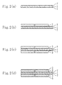
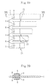
- FIG 1 shows a thin-film piezoelectric bimorph element according to Embodiment 1 of the present invention.
- the thin-film piezoelectric bimorph element comprises a metal thin plate 1 made of stainless steel and having a thickness of 50 to 200 ⁇ m (preferably 50 to 100 ⁇ m).
- a first piezoelectric thin film 2 is provided on one of the both surfaces (upper surface) of the metal thin plate 1 which are in opposing relation to each other along the thickness thereof with a diffusion preventing film 7 interposed therebetween, which will be described later, while a second piezoelectric thin film 3 is provided on the other of the both surfaces (lower surface) of the metal thin plate 1 which are in opposing relation to each other along the thickness thereof with another diffusion preventing film 7 interposed therebetween.
- the first and second piezoelectric thin films 2 and 3 having equal thicknesses are formed by sputtering on the both surfaces of the metal thin plate 1 as a substrate for film formation which are in opposing relation to each other along the thickness thereof, while the respective states of polarizations thereof are controlled.
- the directions of polarizations of the first and second piezoelectric thin films 2 and 3 are opposite to each other (see the arrows in Figure 1 ). That is, the directions of polarizations of the first and second piezoelectric thin films 2 and 3 are oppositely oriented relative to the metal thin plate 1 along the thickness thereof (upward in the first piezoelectric thin film 2 and downward in the second piezoelectric thin film 3 ).
- the thickness of each of the first and second piezoelectric thin films 2 and 3 is preferably 10 ⁇ m or less.
- the arrangement allows effective scaling down of the thin-film piezoelectric bimorph element.
- the first and second piezoelectric thin films 2 and 3 can be formed in a relatively short period of time and the compositions of the first and second piezoelectric thin films 2 and 3 can be controlled easily.
- each of the first and second piezoelectric thin films 2 and 3 is represented appropriately by Pb p La q Ti r Zr s O 3 provided that the values of p, q, r, and s satisfy any of the following numerical expressions (1) to (3).
- Pb 0.9 La 0.1 Ti 0.975 O 3 (PLT), PbTiO 3 , PbZr 0.50 Ti 0.50 O 3 (PZT), Pb 0.9 La 0.1 (Zr 0.1 Ti 0.9 ) 0.975 O 3 (PLZT), or the like is particularly preferred.
- a pair of electrode films 5 each made of Pt and having a thickness of 0.1 to 0.2 ⁇ m are formed on the surface (upper surface) of the first piezoelectric thin film 2 which is opposite to the metal thin plate 1 and on the surface (lower surface) of the second piezoelectric thin film 3 which is opposite to the metal thin plate 1 .
- a pair of diffusion preventing films 7 for preventing the diffusion of a substance (especially Cr) composing the metal thin plate 1 in the first and second piezoelectric thin films 2 and 3 are provided between the metal thin plate 1 and the first piezoelectric thin film 2 and between the metal thin plate 1 and the second piezoelectric thin film 3 .
- Each of the diffusion preventing films 7 is made of Pt, similarly to each of the electrode films 5 , and has a thickness adjusted to 0.1 to 0.2 ⁇ m. Although each of the diffusion preventing films 7 also functions as an electrode, each of the diffusion preventing films 7 is not necessarily required.
- the thin-film piezoelectric bimorph element bends to protrude downward.
- the thin-film piezoelectric bimorph element can be used as an actuator which is operated with the application of a voltage.
- the thin-film piezoelectric bimorph element When the thin-film piezoelectric bimorph element is deformed by an external force, on the other hand, a voltage is generated between the two electrode films 5 , which allows the thin-film piezoelectric bimorph element to be used as a mechanical detector for detecting a dynamic amount such as acceleration or pressure.
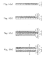
- the pair of diffusion preventing films 7 are formed on the both surfaces of the metal plate 1 as a substrate for film formation which are in opposing relation to each other along the thickness thereof (see Figure 2 (a)).
- the diffusion preventing films 7 are formed by, e.g., RF magnetron sputtering using a gas mixture of Ar and oxygen (at a mixture ratio of 95/5 to 80/20) under such conditions that the temperature of the metal thin plate 1 (substrate temperature) is 500 to 700 °C, the pressure of the sputter gas is 0.1 to 5 Pa, and the density of RF power applied is 1 to 5 W/cm 2 (at a frequency of 13.56 MHz). After one hour of film formation, the diffusion preventing films 7 each having a thickness of about 0.15 ⁇ m are obtained.
- the first and second piezoelectric thin films 2 and 3 are formed by sputtering on the respective surfaces of the two diffusion preventing films 7 which are opposite to the metal thin plate 1 , while the respective states of polarizations thereof are controlled.
- the first piezoelectric thin film 2 is formed first on the upper surface of one of the diffusion preventing films 7 that has been oriented upward (see Figure 2(b) ).
- Table 1 shows specific conditions for film formation when the first piezoelectric thin film 2 made of a material such as PLT, PbTiO 3 , PZT, or PLZT is formed by RF magnetron sputtering (at a frequency of 13.56 MHz).
- the first piezoelectric thin film 2 formed under the foregoing conditions has a tetragonal crystal structure and the direction of polarization thereof becomes upward (it is also possible to render the direction of polarization downward by adjusting the temperature of the metal thin plate 1 to a level higher than listed in Table 1).
- the polarization axes are oriented equally in the (001) direction. This may be because the metal thin plate 1 reduces a thermal stress in the first piezoelectric thin film 2 in the cooling process after film formation since the thermal expansion coefficient of the metal thin plate 1 is higher than that of the first piezoelectric thin film 2 .
- the metal thin plate 1 is vertically inverted and the second piezoelectric thin film 3 is formed under the same conditions as used in forming the first piezoelectric thin film 2 (see Figure 2(c) ).
- the direction of polarization of the second piezoelectric thin film 3 also becomes upward, while the direction of polarization of the first piezoelectric thin film 2 is downward as a result of the vertical inversion. Therefore, the directions of polarizations of the first and second piezoelectric thin films 2 and 3 are opposite to each other.
- the electrode films 5 are formed on the respective surfaces of the first and second piezoelectric thin films 2 and 3 which are opposite to the metal thin plate 1 (see Figure 2(d) ).
- a specific method of forming each of the electrode films 5 is the same as used in forming the diffusion preventing films 7 .
- first and second piezoelectric thin films 2 and 3 and the pair of electrodes 5 are patterned optionally to have proper configurations depending on the application of the thin-film piezoelectric bimorph element.
- the pair of electrode films 5 are patterned first by sputter etching. If the electrode films 5 are etched in a vacuum of about 8 Pa by using Ar gas at a flow rate of 10 sccm with a plasma power of 170 W, the etching is completed in about 15 minutes.
- the first and second piezoelectric thin films 2 and 3 are patterned by chemical etching.
- Table 2 shows process conditions for chemical etching when the first and second piezoelectric thin films 2 and 3 are made of a material such as PLT, PbTiO 3 , PZT, or PLZT.
- the pair of diffusion preventing films 7 are patterned by the same method as used in patterning the pair of electrode films 5 . If necessary, the metal thin plate 1 is processed by etching or by using a laser, whereby the thin-film piezoelectric bimorph element is completed.
- Embodiment 1 has formed the first and second piezoelectric thin films 2 and 3 by sputtering on the both surfaces of the metal thin plate 1 which are in opposing relation to each other along the thickness thereof with the pair of diffusion preventing films 7 interposed therebetween, comparatively thin first and second piezoelectric thin films 2 and 3 can be formed uniformly and bonded securely to the metal thin plate 1 (this is also true in the absence of the diffusion preventing films 7 ).
- This provides a thin-film piezoelectric bimorph element which is more compact than in the case where the piezoelectric members are bonded adhesively to the metal plate and eliminates sensitivity variations resulting from the bonding of the first and second piezoelectric thin films 2 and 3 to the metal thin plate 1 .
- the first and second piezoelectric thin films 2 and 3 can be formed easily by sputtering and the respective directions of polarizations thereof can be controlled easily by adjusting the temperature of the metal thin plate 1 . Accordingly, the thin-film piezoelectric bimorph element can be manufactured at a low cost.
- first and second piezoelectric thin films 2 and 3 and the like can be patterned easily by etching, which allows simultaneous manufacturing of a plurality of thin-film piezoelectric bimorph elements.
- the material of the metal thin plate 1 is not limited to stainless steel.
- the metal thin plate 1 may also be made of a metal such as Ti, Pt, phosphor bronze, or beryllium bronze.
- the material of the diffusion preventing films 7 may be a precious metal such as Au, Pd, or Ag other than Pt.
- a metal other than a precious metal and an anticorrosive metal this is also true in the following Embodiments 2 to 8 ).
- the diffusion preventing films 7 may also be formed by chemical vapor deposition, plating, or the like instead of sputtering.
- the diffusion preventing films 7 need not necessarily be formed entirely over the both surfaces of the metal thin plate 1 which are in opposing relation to each other along the thickness thereof. It is sufficient to form the diffusion preventing films 7 on at least portions to be formed with the first and second piezoelectric thin films 2 and 3 .
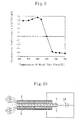
- the directions of the polarization axes of the first and second piezoelectric thin films 2 and 3 change depending on the composition thereof. If the composition of the first and second piezoelectric thin films 2 and 3 is PbZr x Ti 1-x O 3 , e.g., the crystal structure thereof change with the value of X (proportion of Zn to Ti), as shown in Figure 3 . If the value of X is small, the crystal structure is tetragonal and the polarization axes (Ps) are oriented in the (001) direction. If the value of X is large, the crystal structure is rhombohedral and the polarization axes are oriented in the (111) direction.
- the polarization axes are oriented in the (001) direction if the values of p, q, r and s in Pb p La q Ti r Zr s O 3 representing the composition of the first and second piezoelectric thin films 2 and 3 satisfy either of the following numerical expressions (a) and (b).
- the crystal structure of the first and second piezoelectric thin films 2 and 3 is not limited to a tetragonal system in which the polarization axes are oriented in the (001) direction and may be a rhombohedral system in which the polarization axes are oriented in the (111) direction, as described above.
- FIG 4 shows Embodiment 2 of the present invention (in each of the following embodiments, the detailed description of the same components as shown in Figure 1 will be omitted by retaining the same reference numerals), in which each of first and second piezoelectric thin films 2 and 3 has a multilayer structure.
- the first piezoelectric thin film 2 in Embodiment 2 is composed of a plurality of (three in the present embodiment) piezoelectric layers 2a , 2b , and 2c stacked along the thickness of the metal thin plate 1 .
- the piezoelectric layers 2a , 2b , and 2c are constituted to have a piezoelectric constant which decreases gradually with approach toward the metal thin plate 1 .
- the composition of the first piezoelectric thin film 2 is represented by PbZr x Ti 1-x O 3 as described above, the value of X is changed appropriately for each of the piezoelectric layers 2a, 2b , and 2c to change the proportion of Zn to Ti.
- the second piezoelectric thin film 3 is also composed of three piezoelectric layers 3a , 3b , and 3c stacked along the thickness of the metal thin plate 1 which are also constituted to have a piezoelectric constant which decreases gradually with approach toward the metal thin plate 1 .
- the directions of polarizations of the first and second piezoelectric thin films 2 and 3 are the same as in Embodiment 1 so that the directions of polarizations of the individual piezoelectric layers 2a, 2b , and 2c of the first piezoelectric thin film 2 are upward and the directions of polarizations of the individual piezoelectric layers 3a, 3b , and 3c of the second piezoelectric thin films 3 are downward.
- a pair of diffusion preventing films 7 are formed on the both surfaces of the metal thin plate 1 which are in opposing relation to each other along the thickness thereof (see Figure 5(a) ), similarly to Embodiment 1.
- the first piezoelectric thin film 2 is formed on the upper surface of one of the diffusion preventing films 7 that has been oriented upward.
- the three piezoelectric layers 2a , 2b , and 2c having different piezoelectric constants are stacked along the thickness of the metal thin plate 1 such that the piezoelectric constants thereof are in increasing order (see Figure 5(b) ).
- the method of forming the piezoelectric layers 2a , 2b , and 2c is the same as the method of forming the first and second piezoelectric thin films 2 and 3 used in Embodiment 1.
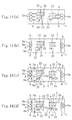
- composition control is performed by using, e.g., a multiple sputtering system as shown in Figure 6 . That is, if the composition is represented by PbZr x Ti 1-x O 3 , the composition is varied by controlling RF power applied to each of metal targets 12 of Pb, Ti, and Zn by using a controller 13 .
- a heater for heating the metal thin plate 1 to a specified temperature is designated at 14 .
- the second piezoelectric thin film 3 is formed on the upper surface of the other of the diffusion preventing films 7 that has been oriented upward.
- the three piezoelectric layers 3a , 3b , and 3c having different piezoelectric constants are stacked such that the piezoelectric constants thereof are in increasing order (see Figure 5(c) ), similarly to the first piezoelectric thin film 2 .
- Table 3 shows the compositions of the piezoelectric layers 2a, 2b , and 2c of the first piezoelectric thin film 2 and of the piezoelectric layers 3a, 3b , and 3c of the second piezoelectric thin film 3 and conditions for film formation.
- Reference Numerals of Piezoelectric Layers Composition of Piezoelectric Thin Film Temperature of Metal Thin Plate Film Thickness ( ⁇ m) 2a, 3a PbZr 0.30 Ti 0.70 O 3 570 to 630 °C 1.0 2b, 3b PbZr 0.45 Ti 0.55 O 3 570 to 630 °C 1.0 2c, 3c PbZr 0.52 Ti 0.48 O 3 570 to 630 °C 1.0
- the electrode films 5 are formed on the respective surfaces of the first and metal piezoelectric thin films 2 and 3 which are opposite to the metal thin plate 1 (see Figure 5(d) ), similarly to Embodiment 1. Thereafter, the first and second piezoelectric thin films 2 and 3 , the pair of electrode films 5 , and the like are patterned if necessary.
- the first and second piezoelectric thin films 2 and 3 are less likely to peel off the metal thin plate 1 .
- the metal thin plate 1 neither expands nor contracts, the rigidity thereof is by far larger than that of the first and second piezoelectric thin films 2 and 3 so that a high tensile stress or compressive stress is produced at the joints between the first and second piezoelectric thins films 2 and 3 and the metal thin plate 1 .
- the first and second piezoelectric tin films 2 and 3 are particularly susceptible to a tensile stress, the durability on the side on which a tensile stress is produced presents a problem.
- the piezoelectric constants of the piezoelectric layers 2a and 3a which are closest to the metal thin plate 1 have been reduced considerably, as described above, so that a strain resulting from the expansion or contraction of the piezoelectric layers 2a and 3a is slight. Accordingly, the stress produced at the portions of the first and second piezoelectric thin films 2 and 3 joined with the metal thin plate 1 can be reduced. Even over a prolonged period of use, therefore, the first and second piezoelectric thin films 2 and 3 will not peel off the metal thin plate 1 so that the durability of the thin-plate piezoelectric bimorph element is improved.
- each of the first and second piezoelectric thin films 2 and 3 has the multilayer structure in Embodiment 2, they may have a piezoelectric constant which increases gradually with distance from the metal thin plate 1 toward the opposite side thereof in a single-layer structure as used in Embodiment 1, not in a multilayer structure.
- the composition is varied gradually in forming the first and second piezoelectric thin films 2 and 3 such that the piezoelectric constant increases gradually with distance from the metal thin plate 1 toward the opposite side thereof.
- Figure 7 shows Embodiment 3 of the present invention, in which the directions of polarizations of the first and second piezoelectric thin films 2 and 3 are the same. That is, the direction of polarization of the first piezoelectric thin film 2 is from the side opposite to the metal thin plate 1 toward the metal thin plate 1 (downward), which is different from Embodiments 1 and 2 .
- the thin-plate piezoelectric bimorph element bends to protrude downward.
- the diffusion preventing films 7 are formed on the both surfaces of the metal thin plate 1 which are in opposing relation to each other along the thickness thereof, similarly to Embodiment 1 (see Figure 8(a) ).
- the first piezoelectric thin film 2 is formed on one of the diffusion preventing films 7 that has been oriented upward (see Figure 8(b) ).
- the temperature of the metal thin plate 1 is adjusted to be higher than the temperature range (570 to 630 °C) listed in Table 1 so that the direction of polarization of the first piezoelectric thin film 2 is oriented downward (the conditions other than the temperature of the metal thin plate 1 are the same as listed in Table 1).
- the temperature of the metal thin plate 1 is adjusted to 670 to 720 °C.
- the relationship between the pyroelectric coefficient and the temperature of the metal thin plate 1 is as shown in Figure 9 (the positive direction of a pyroelectric current is from the side opposite to the metal thin plate 1 toward the meal thin plate 1 ). If the temperature of the metal thin plate 1 is adjusted to 670 to 720 °C, the pyroelectric current flows in a negative direction so that the direction of polarization is from the side opposite to the metal thin plate 1 toward the metal thin plate 1 (downward). If the temperature of the metal thin plate 1 is adjusted to 570 to 630 °C as in Embodiment 1, the pyroelectric current flows in the positive direction so that the direction of polarization is from the metal thin plate 1 toward the opposite side thereof.
- the other of the diffusion preventing films 7 is oriented upward and the second piezoelectric thin film 3 is formed by sputtering on the upper surface thereof (see Figure 8(c) ).
- the temperature of the meal thin plate 1 is adjusted to 570 to 630 °C.
- the second piezoelectric thin film 3 is formed by sputtering, while the temperature of the metal thin plate 1 is adjusted to a level lower than the temperature during the formation of the first piezoelectric thin film 2 and the state of polarization thereof is controlled.
- the direction of polarization of the second piezoelectric thin film 3 is from the metal thin plate 1 toward the opposite side thereof (upward) so that the directions of polarizations of the first and second piezoelectric thin films 2 and 3 are the same.
- the pair of electrode films 5 are formed on the respective surfaces of the first and second piezoelectric thin films 2 and 3 which are opposite to the metal thin plate 1 (see Figure 8(d) ), similarly to Embodiment 1. Thereafter, the first and second piezoelectric thin films 2 and 3 and the pair of electrode films 5 are patterned as required.
- Embodiment 3 has also formed the first and second piezoelectric thin films 2 and 3 by sputtering on the both surfaces of the metal thin plate 1 which are in opposing relation to each other along the thickness thereof, similarly to Embodiment 1, the same effects as obtained in Embodiment 1 are obtained.
- each of the first and second piezoelectric thin films 2 and 3 may be formed to have a multilayer structure or a piezoelectric constant which gradually increases with distance from the metal thin plate 1 toward the opposite side thereof.
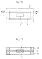
- Figures 11 and 12 show a mechanical detector according to Embodiment 4 of the present invention.
- the mechanical detector is used as a sensor for sensing a dynamic amount such as pressure or acceleration.
- the mechanical detector also comprises: a metal thin plate 1 made of stainless steel; first and second piezoelectric thin films 2 and 3 formed by sputtering on the both surfaces of the metal thin plate 1 which are in opposing relation to each other along the thickness thereof, while the respective states of polarizations thereof are controlled; and a pair of electrode films 5 made of Pt provided on the respective surfaces of the first and second piezoelectric thin films 2 and 3 which are opposite to the metal thin plate 1 (referred to as outer electrode films in Embodiments 4, 5, and 8 for the distinction between the electric films 5 and inner electrode films 8 , which will be described later).
- the mechanical detector is provided with five dynamic amount detecting portions 21 .
- the pair of outer electrode films 5 are patterned to be located correspondingly to the individual dynamic amount detecting portions 21 .
- Holes 22 for forming the detecting portions are formed in the metal thin plate 1 and in the first and second piezoelectric thin films 2 and 3 to surround the dynamic amount detecting portions 21 .
- the holes 22 for forming the detecting portions sequentially penetrate the metal thin plate 1 and the first and second piezoelectric thin films 2 and 3 .
- the three dynamic amount detecting portions 21 located on the left hand of Figure 11 are configured as cantilevers, while the two dynamic amount detecting portions 21 located on the right hand of Figure 11 are configured as fixed-end beams, so that the dynamic amount detecting portions are likely to be deformed.
- the mechanical detector 21 is composed of thin-film piezoelectric bimorph elements each having the metal thin plate 1 , the first and second piezoelectric thin films 2 and 3 formed by sputtering on the both surfaces of the metal thin plate 1 which are in opposing relation to each other along the thickness thereof, while the respective states of polarizations thereof are controlled, and the pair of outer electrode films 5 provided on the respective surfaces of the first and second piezoelectric thin films 2 and 3 which are opposite to the metal thin plate 1 .
- the dynamic amount detecting portions 21 are formed to have different lengths, which renders the respective natural frequencies of the dynamic amount detecting portions 21 different from each other.
- the directions of polarizations of the first and second piezoelectric thin films 2 and 3 may be opposite to each other, as in Embodiment 1, or the same, as in Embodiment 3.
- the pair of inner electrode films 8 made of Pt (which perform the same function in the individual dynamic amount detecting portions 21 as the diffusion preventing films 7 of the thin-film piezoelectric bimorph elements of Embodiments 1 to 3) are formed by patterning to be located correspondingly to the individual dynamic amount detecting portions 21 between the metal thin plate 1 and the first and second piezoelectric thin films 2 and 3 .
- Each of the inner electrode films 8 has one end portion provided with an electric contact portion 8a , which is uncovered with the first and second piezoelectric thin films 2 and 3 .
- Each of the outer electrode films 5 also has an electric contact portion 5a adjacent the corresponding one of the dynamic amount detecting portions 21 .
- the pair of inner electrode films 8 are formed on the both surfaces of the metal thin plate 1 which are in opposing relation to each other along the thickness thereof.
- the inner electrode films 8 are then patterned by etching into specified configurations (see Figure 13(a) ).
- a method of forming the inner electrode films 8 is the same as the method of forming the diffusion preventing films 7 used in Embodiment 1.
- a method of etching is the same as the method of etching the electrode films 5 used in Embodiment 1.
- the first and second piezoelectric thin films 2 and 3 are formed by sputtering on the both surfaces of the metal thin plate 1 (on the portions other than the right and left end portions on which the electric contact portions 8a of the inner electrode films 8 are located) which are formed with the respective inner electrode films 8 and in opposing relation to each other along the thickness thereof, while the respective states of polarizations thereof are controlled (see Figure 13(b) ), similarly to Embodiments 1 to 3.
- the pair of outer electrode films 5 are formed on the respective surfaces of the first and second piezoelectric thin films 2 and 3 which are opposite to the metal thin plate 1 .
- the outer electrode films 5 are then patterned by etching into specified configurations (see Figure 13(c) ).
- a method of forming and etching the outer electrode films 5 is the same as the method of forming and etching the electrode films 5 used in Embodiment 1.
- the portions of the first and second piezoelectric thin films 2 and 3 corresponding to the periphery of the outer electrode films 5 are etched in the same manner as in Embodiment 1 (see Table 2). Thereafter, the portion of the metal thin plate 1 corresponding to the periphery of the outer electrode films 5 is processed by etching, so that the holes 22 for forming the detecting portions (see Figure 13(d) ) are formed and the dynamic amount detecting portions 21 having specified configurations are thereby formed.
- Figure 14 illustrates another method of manufacturing the foregoing mechanical detector, in which through holes 23 having generally the same configurations as the holes 22 for forming the detecting portions are formed preliminarily in the metal thin plate 1 .
- the portions corresponding to the three dynamic amount detecting portions 21 configured as cantilevers have their tip portions coupled to the portions of the inner surfaces of the through holes 23 with fine coupling portions 24 such that they are not deformed in the manufacturing process.
- the through holes 23 are formed first in the metal thin plate 1 such that the portions corresponding to the dynamic amount detecting portions 21 and the coupling portions 24 are formed. Then, the pair of inner electrode films 8 are formed on the both surfaces of the metal thin plate 1 formed with the through holes 23 which are in opposing relation to each other along the thickness thereof. The inner electrode films 8 are then patterned by etching into specified configurations (see Figure 14(a) ). Next, the first and second piezoelectric thin films 2 and 3 are formed on the respective surfaces of the metal thin plate 1 which are in opposing relation to each other along the thickness thereof and formed with the respective inner electrode films 8 (see Figure 14(b) ).
- the first and second piezoelectric thin films 2 and 3 are formed not to cover the through holes 23 of the metal thin plate 1 .
- the pair of outer electrode films 5 are formed on the respective surfaces of the first and second piezoelectric thin films 2 and 3 which are opposite to the metal thin plate 1 .
- the outer electrode films 5 are then patterned by etching into specified configurations (see Figure 14(c) ).
- the coupling portions 24 are subjected to a cutting process using a laser (which may also be subjected to an etching process), so that the holes 22 for forming the detecting portions are formed (the through holes 23 which are unformed with the coupling portions 24 serve as the holes 22 for forming the detecting portions without any alterations) and the mechanical detector comprising the dynamic amount detecting portions 21 having specified configurations are thereby completed.
- Embodiment 4 has thus formed the dynamic amount detecting portions 21 by forming the first and second piezoelectric thin films 2 and 3 by sputtering on the both surfaces of the metal thin plate 1 which are in opposing relation to each other along the thickness thereof, a compact and high-performance mechanical detector can be obtained easily at low cost. Moreover, since the plurality of dynamic amount detecting portions 21 can be formed simultaneously and easily, the mechanical detector can sense a wide variety of frequencies if it is used as an acceleration sensor or the like by rending the lengths of the plurality of dynamic amount detecting portions 21 , i.e., the natural frequencies thereof different from each other.
- FIG. 15 shows Embodiment 5 of the present invention, in which three dynamic amount detecting portions 21 each composed of a thin-film piezoelectric bimorph element (the first, second, and third dynamic amount detecting portions 21a, 21b , and 21c ) are provided, similarly to Embodiment 4, so as to bend in different directions. It is to be noted that the metal thin plate 1 and the individual films are depicted in Figure 15 by omitting the thicknesses thereof.
- the first dynamic amount detecting portion 21a of Embodiment 5 extends in a direction (the y-direction in Figure 15 ) parallel to the both surfaces of the metal thin plate 1 which are in opposing relation to each other along the thickness thereof and bends in the direction (the z-direction in Figure 15 ) of the thickness of the metal thin plate 1 , similarly to Embodiment 4 .
- the second dynamic amount detecting portion 21b of Embodiment 5 is bent at the proximal end thereof to extend in the z-direction and bend in the x-direction which is perpendicular to the y- and z-directions
- the third mechanical detector 21c of Embodiment 5 is bent at the proximal end thereof to extend in the z-direction and bend in the y-direction.
- the first to third dynamic amount detecting portions 21a , 21b , and 21c are designed to bend in the directions perpendicular to each other.
- the mechanical detector is for triaxial detection and capable of detecting respective dynamic amounts in the x-, y-, and z-directions.
- the method of manufacturing the mechanical detector is generally the same as in Embodiment 4 until the process reaches the step of forming the holes 22 for forming the detecting portions .
- the second and third dynamic amount detecting portions 21b and 21c are bent by 90° at the proximal ends thereof (a bending process is performed with respect to the metal thin plate 1 ) into specified configurations.
- a heat treatment involving heating and rapid cooling may also be performed with respect to the bent portions (proximal ends) or, alternatively, a hardening resin may also be applied to the bent portions, as required.
- the bent portions are fixed reliably and the bending angle is stable over a long period of time.
- Embodiment 4 the same effects as obtained in Embodiment 4 are also obtainable in Embodiment 5 and pressure or acceleration acting in mutually perpendicular triaxial directions can be detected by a single mechanical detector.
- each of the first to third dynamic amount detecting portions 21a, 21b , and 21c is provided on a one-by-one basis in Embodiment 5, each of the first to third dynamic amount detecting portions 21a, 21b , and 21c may be provided in a plural number. In short, plural sets of first to third dynamic amount detecting portions 21a, 21b , and 21c may be provided. In that case, the first to third dynamic amount detecting portions 21a, 21b , and 21c in different sets preferably have different lengths (natural frequencies).
- the first to third dynamic amount detecting portions 21a , 21b , and 21c may bend in any directions.
- the directions in which the first to third dynamic amount detecting portions 21a, 21b , and 21c bend are determined appropriately depending on the direction of a dynamic amount to be detected.
- Figure 16 shows an inkjet head according to Embodiment 6 of the present invention.
- the inkjet head comprises a head main body 31 formed with a plurality of depressed portions 32 for pressure chambers having supply ports 32a for ink supply and discharge ports 32b for ink discharge.
- the depressed portions 32 are arranged in rows (two rows in the present embodiment) in a direction perpendicular to the paper surface of Figure 16 .
- the supply ports 32a are connected to ink supply passages 35 extending in the direction in which the rows of depressed portions 2 are arranged.
- the ink supply passages 35 are connected to an ink tank not shown.
- the discharge ports 32b are connected to nozzle slots 36 provided in the bottom surface of the head main body 31 for the respective depressed portions 32 on a one-by-one basis.
- An actuator 41 which covers the depressed portions 32 to compose the pressure chambers 33 in combination with the depressed portions 32 is provided on the upper surface (the surface formed with the depressed portions) of the head main body 31 .
- the actuator 41 causes ink within the pressure chambers 33 to be discharged from the discharge ports 32 and from the nozzle slots 36 such that the ink adheres to a recording sheet disposed in opposing relation to the bottom surface of the head main body 31 .
- the actuator 41 is composed of thin-film piezoelectric bimorph elements each having: a metal thin plate 1 made of stainless steel; first and second piezoelectric thin films 2 and 3 formed by sputtering on the both surfaces of the metal thin plate 1 which are in opposing relation to each other along the thickness thereof, while the respective states of polarizations of the first and second piezoelectric thin films 2 and 3 are controlled; and a pair of electrode films 5 made of Pt and provided on the respective surfaces of the first and second piezoelectric thin films 2 and 3 which are opposite to the metal thin plate 1 .
- the directions of polarizations of the first and second piezoelectric thin films 2 and 3 may be opposite to each other as in Embodiment 1 or may be the same as in Embodiment 3.
- the actuator 41 has drive portions 41a provided at portions corresponding to the individual depressed portions 32 of the head main body 31 .
- the first and second piezoelectric thin films 2 and 3 and the pair of electrode films 5 are patterned to be located correspondingly to the individual drive portions 41 .
- a pair of diffusion preventing films 7 are provided entirely over the metal thin plate 1 and between the metal thin plate 1 and the first and second piezoelectric thin films 2 and 3 , similarly to the thin-film piezoelectric bimorph elements according to Embodiments 1 to 3.
- the portions of the actuator 41 other than the drive portions 41a are fixed to the upper surface of the head main body 31 with an adhesive agent 42 interposed therebetween.
- the metal thin plate 1 is fixed adhesively to the upper surface of the head main body 31 with the diffusion preventing film 7 interposed therebetween and both the second piezoelectric thin film 3 and the electrode film 5 on the second piezoelectric thin film 3 are located within the depressed portions 32 of the head main body 31 .
- the second piezoelectric thin film 3 and the electrode film 5 on the second piezoelectric thin film 3 are exposed to the ink so that each of the films 3 and 5 is preferably covered with, e.g., a thin organic or inorganic insulating film, though it is not depicted.
- the actuator 41 selectively applies, for each of the drive portions 41a , a pulse-like voltage to the first and second piezoelectric thin films 2 and 3 .
- Each of the drive portions 41a is deformed on a rising edge of the pulse voltage in such a manner as to protrude downward. The deformation produces a pressure in the pressure chamber 33 so that the ink within the pressure chamber 33 is discharged under the pressure from the discharge port 32b and from the nozzle slot 36 to the outside to adhere in dots to the paper surface of the recording sheet.
- the drive portion 41a returns to the original state so that the ink is filled in the pressure chamber 33 via the ink supply passage 35 and the supply port 32a .
- the pair of diffusion preventing films 7 are formed on the both surfaces of the metal thin plate 1 which are in opposing relation to each other along the thickness thereof (see Figure 17(a) ), similarly to Embodiment 1.
- the first and second piezoelectric thin films 2 and 3 are formed by sputtering, while the respective states of polarizations thereof are controlled (see Figure 17(b) ), similarly to Embodiment 1 or 3.
- each of the pair of electrode films 5 and of the first and second piezoelectric thin films 2 and 3 is patterned into a specified configuration, whereby the drive portions 41a are formed (see Figure 17(c) ).
- the metal thin plate 1 is fixed adhesively to the head main body 31 preliminarily formed with the depressed portions 32 for pressure chambers, whereby the inkjet head is completed (see Figure 17(d) ).
- Embodiment 6 has thus formed the actuator 41 by forming the first and second piezoelectric thin films 2 and 3 by sputtering on the both surfaces of the metal thin plate 1 which are in opposing relation to each other along the thickness of thereof, a compact and high-performance actuator 41 can be obtained easily at low cost, similarly to the thin-film piezoelectric bimorph elements of Embodiments 1 and 3, so that the gradation of printing is improved.
- the configuration of the actuator 41 and the placement of the drive portions 41 can be determined arbitrarily. Furthermore, the flexibility of the configuration and size of the inkjet head can be enhanced.
- Figure 18 shows a thin-film piezoelectric bimorph element according to Embodiment 7 of the present invention, in which a pair of diffusion preventing films 7 made of PbZrO 3 or the like which does not have a piezoelectric effect are provided between the first and second piezoelectric thin films 2 and 3 , each having a multilayer structure similarly to Embodiment 2, and the metal thin plate 1 .
- the diffusion preventing films 7 are not metal films and do not function as electrode films but prevent the diffusion of Cr or the like contained in the metal thin plate 1 in the first and second piezoelectric thin films 2 and 3 . Since the diffusion preventing films 7 do not have a piezoelectric effect, it achieves the effect of reducing stresses produced in the piezoelectric layers 2a and 3a of the first and second piezoelectric thin films 2 and 3 closer to the metal thin plate 1 . Therefore, the durability of the thin-film piezoelectric bimorph element can further be increased than in Embodiment 2.
- Figures 19 and 20 show a mechanical detector according to Embodiment 8 of the present invention, which has a structure different from the structure of the mechanical detector in Embodiment 4.
- each of the dynamic amount detecting portions 21 has a proximal portion composed of a metal thin plate 1 , first and second piezoelectric thin films 2 and 3 , an outer electrode film 5 , and an inner electrode film 8 , similarly to the dynamic amount detecting portions 21 in Embodiment 4 , while having a distal portion composed only of the metal thin plate 1 .
- the distal portions of the dynamic amount detecting portions 21 have different lengths, while the proximal portions thereof have equal lengths. Accordingly, the five dynamic amount detecting portions 21 have different natural frequencies.
- the proximal portions of the dynamic amount detecting portions 21 are connected to each other by only the metal thin plate 1 .
- a method of manufacturing such a mechanical detector is also the same as in Embodiment 4 and allows easy and low-cost formation of a compact and high-performance mechanical detector.
- the mechanical detector is used as an acceleration sensor, it can sense a wide variety of frequencies.
- each of the foregoing embodiments has controlled the temperature of the metal thin plate 1 for polarization control, it is also possible to apply an external force to the metal thin plate 1 .
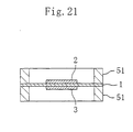
- a description will be given to a method of applying an external force to the metal thin plate 1 with reference to Figure 21 .
- the method uses a circular metal thin plate 1 .
- First and second piezoelectric thin films 2 and 3 are formed with ring-shaped metal rings 51 bonded to the peripheral portions of the both surfaces of the metal thin plate 1 which are in opposing relation to each other along the thickness thereof.
- Each of the metal rings 51 is made of a material having a thermal expansion coefficient higher than that of the metal thin plate 1 .
- the metal thin plate 1 is composed of stainless steel (with a thermal expansion coefficient of 9 to 18 x 10 -6 /°C) or Cr (with a thermal expansion coefficient of 7 x 10 -6 /°C), for example, the metal rings 51 are composed appropriately of Al (with a thermal expansion coefficient of 24 x 10 -6 /°C), Mn (with a thermal expansion coefficient of 23 x 10 -6 /°C), or the like.
- the metal rings 51 By using the metal rings 51 , the metal thin plate 1 can be stretched outwardly diametrically by properly adjusting an ambient temperature during film formation.
- the metal thin plate 1 contracts if a room temperature is restored after film formation such that thermal stresses in the first and second piezoelectric thin films 2 and 3 are reduced and the polarization axes are equally oriented in the (001) direction, as described in Embodiment 1.
- a compressing force also acts on the first and second piezoelectric thin films 2 and 3 at a room temperature. Accordingly, the strengths of the first and second piezoelectric thin films 2 and 3 which are sensitive to a tensile force can be increased.
- first and second piezoelectric thin films 2 and 3 have equal thicknesses in each of the foregoing embodiments, the first and second piezoelectric thin films 2 and 3 may have different thicknesses, as shown in Figure 24 .
- a tensile force constantly acts on the first piezoelectric thin film 2
- a compressive force constantly acts on the second piezoelectric thin film 3
- resistance to the tensile force is also provided if the first piezoelectric thin film 2 is formed to be thicker than the second piezoelectric thin film 3 , as shown in Figure 24 , so that durability is increased.
- the bent configuration is hardly affected since the rigidity of the metal thin plate 1 is by far higher than that of the first and second piezoelectric thin films 2 and 3 .
- a metal thin film 62 having a thickness of about 2 to 10 ⁇ m is formed by sputtering on a substrate 61 for film formation made of MgO (see Figure 25(a) ).
- a first piezoelectric thin film 2 and an electrode film 5 are formed successively on the metal thin film 62 and then patterned (see Figure 25(b) ).
- a MgO film 63 is formed entirely over the metal thin film 62 formed with the first piezoelectric thin film 2 and the electrode film 5 (see Figure 25(c) ). Thereafter, the MgO film 63 is covered with a protective material not shown.
- the substrate 61 for film formation is then molten away by phosphoric acid or the like (see Figure 25(d) ). Thereafter, a second piezoelectric thin film 3 and the electrode film 5 are formed on the surface of the metal thin film 62 from which the substrate 61 for film formation has been removed (see Figure 25(e) ).
- the surface of the metal thin film 62 from which the substrate 61 for film formation has been removed is fixed to a structure 64 such as the head main body 31 (see Figure 25(f) ). Thereafter, the MgO film 63 is removed (see Figure 25(g) ).
- the metal thin plate 1 composed of the metal thin film 62 and having a considerably reduced thickness can be formed. Since the metal thin film 62 is supported by at least one of the substrate 61 for film formation and the MgO film 63 in the manufacturing process, it is free of bending or deformation. Since the first and second piezoelectric thin films 2 and 3 are formed by sputtering, while the respective states of polarizations thereof are controlled, there can be obtained a compact and high-performance thin-film piezoelectric bimorph element, similarly to each of the foregoing embodiments.
Claims (21)
- Elément bimorphe piézoélectrique à couches minces comportant :une plaque mince métallique (1) comportant deux surfaces qui sont en relation opposée l'une avec l'autre suivant l'épaisseur de celle-ci,une paire de couches minces piézoélectriques (2, 3) formées sur les deux dites surfaces de la plaque mince métallique (1) par pulvérisation, alors que les états respectifs des polarisations des couches minces piézoélectriques (2, 3) sont commandées durant ladite pulvérisation, etune paire de couches d'électrodes (5) disposées sur des surfaces respectives des couches minces piézoélectriques (2, 3) qui sont opposées à la plaque mince métallique (1).
- Elément bimorphe piézoélectrique à couches minces selon la revendication 1, dans lequel les directions des polarisations de la paire de couches minces piézoélectriques (2, 3) sont opposées l'une à l'autre.
- Elément bimorphe piézoélectrique à couches minces selon la revendication 1, dans lequel les directions des polarisations de la paire de couches minces piézoélectriques (2, 3) sont les mêmes.
- Elément bimorphe piézoélectrique à couches minces selon la revendication 1, dans lequel chacune des couches minces piézoélectriques (2, 3) est composée d'une pluralité de couches piézoélectriques (2a, 2b, 2c, 3a, 3b, 3c) empilées suivant l'épaisseur des couches de la plaque mince métallique (1),
les couches piézoélectriques (2a, 2b, 2c, 3a, 3b, 3c) présentant une constante piézoélectrique qui diminue progressivement en se rapprochant de la plaque mince métallique (1). - Elément bimorphe piézoélectrique à couches minces selon la revendication 1, dans lequel chacune des couches minces piézoélectriques (2, 3) présente une constante piézoélectrique qui augmente progressivement avec la distance par rapport à la plaque mince métallique (1) vers le côté opposé de celle-ci.
- Elément bimorphe piézoélectrique à couches minces selon la revendication 1, dans lequel chacune des couches minces piézoélectriques (2, 3) présente une épaisseur ajustée à 10 µm ou moins.
- Elément bimorphe piézoélectrique à couches minces selon la revendication 1, dans lequel une paire de couches empêchant une diffusion (7) destinées à empêcher une diffusion d'une substance composant la plaque mince métallique (1) dans les couches minces piézoélectriques (2, 3) sont prévues entre la plaque mince métallique (1) et les couches minces piézoélectriques individuelles (2, 3).
- Détecteur mécanique comportant une partie de détection de valeur dynamique, la partie de détection de valeur dynamique (21) étant composée d'un élément bimorphe piézoélectrique à couches minces selon la revendication 1.
- Détecteur mécanique selon la revendication 8, dans lequel la partie de détection de valeur de dynamique (21) comprend une pluralité de parties de détection de valeur dynamique (21) qui sont prévues pour se courber dans des directions différentes.
- Détecteur mécanique selon la revendication 8, dans lequel la partie de détection de valeur dynamique (21) comprend une pluralité de parties de détection de valeur dynamique (21) présentant des fréquences propres différentes.
- Tête d'injection comprenant :un corps principal de tête (31) muni d'une partie en creux (32) destinée à une chambre de pression, la partie en creux (32) comportant un orifice d'alimentation (32a) destiné à l'alimentation en encre et un orifice de rejet (32b) destiné au rejet de l'encre, etun actionneur destiné à amener l'encre dans la chambre de pression à être rejetée de l'orifice de rejet (32b), l'actionneur étant disposé pour couvrir la partie en creux (32) du corps principal de tête (31) et définir la chambre de pression en combinaison avec la partie en creux (32),l'actionneur étant composé d'un élément bimorphe piézoélectrique à couches minces selon la revendication 1.
- Procédé de fabrication d'un élément bimorphe piézoélectrique à couches minces, le procédé comprenant les étapes consistant à :disposer une plaque mince métallique (1) comportant deux surfaces qui sont en relation opposée l'une avec l'autre suivant l'épaisseur de celle-ci,former une paire de couches minces piézoélectriques (2, 3) sur les deux dites surfaces de la plaque mince métallique (1) par pulvérisation, tout en commandant les états respectifs des polarisations des couches minces piézoélectriques (2, 3) durant ladite pulvérisation, etformer une paire de couches d'électrodes (5) sur des surfaces respectives des couches minces piézoélectriques (2, 3) qui sont opposées à la plaque mince métallique (1).
- Procédé selon la revendication 12, dans lequel l'étape de formation des couches minces piézoélectriques (2, 3) comprend :la formation de la paire de couches minces piézoélectriques (2, 3) de telle sorte que les directions des polarisations de celles-ci soient opposées l'une à l'autre.
- Procédé selon la revendication 12, dans lequel l'étape de formation des couches minces piézoélectriques (2, 3) comprend les étapes consistant à :former les premières couches minces piézoélectriques (2) par pulvérisation sur l'une des deux surfaces de la plaque mince métallique (1) qui sont en relation opposée l'une avec l'autre suivant l'épaisseur de celle-ci, tout en ajustant une température de la plaque mince métallique (1) à un niveau spécifié et en commandant ainsi l'état de polarisation de la première couche mince piézoélectrique (2), etaprès l'étape de formation de la première couche mince piézoélectrique (2), former la seconde couche mince piézoélectrique (3) par pulvérisation sur l'autre des deux surfaces de la plaque mince métallique (1) qui sont en relation opposée l'une avec l'autre suivant l'épaisseur de celle-ci, tout en ajustant la température de la plaque mince métallique (1) à un niveau inférieur au niveau spécifié et en commandant ainsi l'état de la polarisation de la seconde couche mince piézoélectrique (3), la seconde couche mince piézoélectrique (3) présentant la même direction de polarisation que la première couche mince piézoélectrique (2).
- Procédé selon la revendication 12, dans lequel l'étape de formation des couches minces piézoélectriques (2, 3) comprend :la formation de chacune des couches minces piézoélectriques (2, 3) par empilement d'une pluralité de couches piézoélectriques (2a, 2b, 2c, 3a, 3b, 3c) présentant des constantes piézoélectriques différentes suivant l'épaisseur de la plaque mince métallique (1) de sorte que les constantes piézoélectriques soient en nombre croissant.
- Procédé selon la revendication 12, dans lequel l'étape de formation des couches minces piézoélectriques (2, 3) comprend :la formation de chacune des couches minces piézoélectriques (2, 3) de telle sorte qu'une constante piézoélectrique des couches minces piézoélectriques (2, 3) augmente progressivement avec la distance par rapport à la plaque mince métallique (1) vers le côté opposé de celle-ci.
- Procédé selon la revendication 12, comprenant en outre, avant l'étape de formation des couches minces piézoélectriques (2, 3) :l'étape consistant à former une paire de couches empêchant une diffusion (7) destinées à empêcher une diffusion d'une substance composant la plaque mince métallique (1) dans les couches minces piézoélectriques (2, 3) sur les deux surfaces de la plaque mince métallique (1) qui sont en relation opposée l'une avec l'autre suivant l'épaisseur de celle-ci.
- Procédé de fabrication d'un détecteur mécanique comportant une pluralité de parties de détection de valeur dynamique (21), chacune étant composée d'un élément bimorphe piézoélectrique à couches minces, le procédé comprenant les étapes du procédé de fabrication d'un élément bimorphe piézoélectrique à couches minces selon la revendication 12, et
la mise en motif de chacune des couches minces piézoélectriques (2, 3) et des couches d'électrodes (5) suivant une configuration spécifiée, le traitement de la plaque mince métallique (1) suivant une configuration spécifiée après la mise en motif, et ainsi la formation de la pluralité de parties de détection de valeur dynamique (21). - Procédé selon la revendication 18, dans lequel l'étape de formation de la pluralité de parties de détection de valeur dynamique (21) comprend:la formation de la pluralité de parties de détection de valeur dynamique (21), de telle sorte que les parties de détection de valeur dynamique (21) se courbent dans des directions différentes.
- Procédé selon la revendication 18, dans lequel l'étape de formation de la pluralité de parties de détection de valeur dynamique (21) comprend :la formation de la pluralité de parties de détection de valeur dynamique (21) suivant des configurations différentes, de telle sorte que les parties de détection de valeur dynamique (21) présentent des fréquences propres différentes.
- Procédé de fabrication d'une tête à jet d'encre comportant un actionneur destiné au rejet de l'encre, composé d'un élément bimorphe piézoélectrique à couches minces, le procédé comprenant les étapes du procédé de fabrication d'un élément bimorphe piézoélectrique à couches minces selon la revendication 12, et
la mise en motif de chacune des couches minces piézoélectriques (2, 3) et des couches d'électrodes (5) suivant une configuration spécifiée, et
après l'étape de mise en motif, la fixation de la plaque mince métallique (1) sur un corps principal de tête (31) comportant une partie en creux (32) destinée à une chambre de pression qui compose la chambré de pression en combinaison avec la plaque mince métallique (1).
Applications Claiming Priority (2)
| Application Number | Priority Date | Filing Date | Title |
|---|---|---|---|
| JP14205899 | 1999-05-21 | ||
| JP11142058A JP2000332313A (ja) | 1999-05-21 | 1999-05-21 | 薄膜圧電型バイモルフ素子及びその応用 |
Publications (2)
| Publication Number | Publication Date |
|---|---|
| EP1054459A1 EP1054459A1 (fr) | 2000-11-22 |
| EP1054459B1 true EP1054459B1 (fr) | 2002-12-11 |
Family
ID=15306448
Family Applications (1)
| Application Number | Title | Priority Date | Filing Date |
|---|---|---|---|
| EP00110740A Expired - Lifetime EP1054459B1 (fr) | 1999-05-21 | 2000-05-19 | Elément piezo-électrique dimorphe à couche mince, détecteur mécanique et tête d'impression par jet d'encre l'employant et procédés pour sa fabrication |
Country Status (5)
| Country | Link |
|---|---|
| US (1) | US7024738B2 (fr) |
| EP (1) | EP1054459B1 (fr) |
| JP (1) | JP2000332313A (fr) |
| KR (1) | KR100683325B1 (fr) |
| DE (1) | DE60000948T2 (fr) |
Families Citing this family (50)
| Publication number | Priority date | Publication date | Assignee | Title |
|---|---|---|---|---|
| JP4934924B2 (ja) * | 2001-08-09 | 2012-05-23 | パナソニック株式会社 | 強誘電体アクチュエータ素子およびその製造方法 |
| TW546477B (en) * | 2001-08-09 | 2003-08-11 | Matsushita Electric Ind Co Ltd | Drop impact determination system and acceleration sensing element used in the drop impact determination system |
| AU2002215134A1 (en) * | 2001-11-21 | 2003-06-17 | Apogent Robotics Limited | Actuator structure |
| JP3879685B2 (ja) | 2002-03-18 | 2007-02-14 | セイコーエプソン株式会社 | 圧電素子、圧電アクチュエータ、及び、液体噴射ヘッド |
| JP3931823B2 (ja) | 2002-03-18 | 2007-06-20 | セイコーエプソン株式会社 | 圧電アクチュエータ及びその製造方法、並びに、液体噴射ヘッド及びその製造方法 |
| JP3903936B2 (ja) | 2002-03-18 | 2007-04-11 | セイコーエプソン株式会社 | 圧電素子、圧電アクチュエータ、及び、液体噴射ヘッド |
| JP4305016B2 (ja) | 2002-03-18 | 2009-07-29 | セイコーエプソン株式会社 | 圧電アクチュエータユニット、及び、それを用いた液体噴射ヘッド |
| JP3991894B2 (ja) | 2002-03-18 | 2007-10-17 | セイコーエプソン株式会社 | 圧電アクチュエータの製造方法、液体噴射ヘッドの製造方法、及び、アクチュエータ母部材 |
| JP4100202B2 (ja) | 2002-03-18 | 2008-06-11 | セイコーエプソン株式会社 | 圧電アクチュエータ、及び、液体噴射ヘッド |
| KR100478228B1 (ko) * | 2002-06-12 | 2005-03-23 | 재단법인서울대학교산학협력재단 | 분극 방향이 서로 반대인 압전-압전 세라믹 액츄에이터 |
| WO2004023572A1 (fr) * | 2002-08-30 | 2004-03-18 | Usc Corporation | Generateur piezoelectrique |
| AU2003264456A1 (en) * | 2002-10-30 | 2004-05-25 | Sony Corporation | Input device and process for manufacturing the same, portable electronic apparatus comprising input device |
| JP3867664B2 (ja) * | 2002-12-12 | 2007-01-10 | ソニー株式会社 | 入力装置、携帯型情報処理装置、リモートコントロール装置、および入力装置における圧電アクチュエータ駆動制御方法 |
| US6964201B2 (en) * | 2003-02-25 | 2005-11-15 | Palo Alto Research Center Incorporated | Large dimension, flexible piezoelectric ceramic tapes |
| US7089635B2 (en) | 2003-02-25 | 2006-08-15 | Palo Alto Research Center, Incorporated | Methods to make piezoelectric ceramic thick film arrays and elements |
| US6895645B2 (en) * | 2003-02-25 | 2005-05-24 | Palo Alto Research Center Incorporated | Methods to make bimorph MEMS devices |
| JP4593905B2 (ja) * | 2003-06-30 | 2010-12-08 | 京セラ株式会社 | 圧電アクチュエータおよびその製造方法、並びに液体吐出装置 |
| JP4058018B2 (ja) * | 2003-12-16 | 2008-03-05 | 松下電器産業株式会社 | 圧電素子及びその製造方法、並びにその圧電素子を備えたインクジェットヘッド、インクジェット式記録装置及び角速度センサ |
| US7701119B2 (en) | 2003-12-26 | 2010-04-20 | Nec Corporation | Piezoelectric actuator |
| JP4737375B2 (ja) * | 2004-03-11 | 2011-07-27 | セイコーエプソン株式会社 | アクチュエータ装置の製造方法及び液体噴射ヘッドの製造方法並びに液体噴射装置の製造方法 |
| US20060012646A1 (en) * | 2004-07-13 | 2006-01-19 | Brother Kogyo Kabushiki Kaisha | Piezoelectric actuator, ink jet head, and method of manufacturing them |
| EP1616700A1 (fr) * | 2004-07-13 | 2006-01-18 | Brother Kogyo Kabushiki Kaisha | Actionneur piézoélectrique, tête jet d'encre et leur méthode de fabrication |
| US7419252B2 (en) * | 2004-07-13 | 2008-09-02 | Brother Kogyo Kabushiki Kaisha | Ink jet head, piezo-electric actuator, and method of manufacturing them |
| US7239064B1 (en) | 2004-10-15 | 2007-07-03 | Morgan Research Corporation | Resettable latching MEMS temperature sensor apparatus and method |
| WO2006097522A1 (fr) * | 2005-03-18 | 2006-09-21 | Bae Systems Plc | Actionneur |
| US20070041273A1 (en) * | 2005-06-21 | 2007-02-22 | Shertukde Hemchandra M | Acoustic sensor |
| JP4696754B2 (ja) * | 2005-07-26 | 2011-06-08 | Tdk株式会社 | 圧電薄膜振動子およびその製造方法、並びにそれを用いた駆動装置および圧電モータ |
| JP5063892B2 (ja) * | 2005-12-20 | 2012-10-31 | 富士フイルム株式会社 | 液体吐出ヘッドの製造方法 |
| EP1953841B1 (fr) * | 2007-01-30 | 2009-12-02 | Delphi Technologies, Inc. | Procédé de fabrication d'un actionneur piézo-électrique |
| DE602007001155D1 (de) * | 2006-03-17 | 2009-07-09 | Delphi Tech Inc | Piezoelektrischer Aktor |
| WO2009051166A1 (fr) * | 2007-10-16 | 2009-04-23 | Murata Manufacturing Co., Ltd. | Dispositif vibrant, et pompe piézoélectrique |
| JP5636730B2 (ja) * | 2010-04-28 | 2014-12-10 | パナソニック株式会社 | 角速度センサ素子およびその製造方法 |
| KR101187465B1 (ko) | 2011-01-31 | 2012-10-02 | 한국산업기술대학교산학협력단 | 다층 졸겔층을 갖는 압전 세라믹 소자 |
| RU2472253C1 (ru) * | 2011-08-17 | 2013-01-10 | Федеральное государственное бюджетное образовательное учреждение высшего профессионального образования "Тверской государственный университет" | Пьезоэлектрический прибор и способ его изготовления |
| JP5979369B2 (ja) * | 2011-10-03 | 2016-08-24 | セイコーエプソン株式会社 | 発電装置、電子機器、移動手段、電池、及び、発電装置の制御方法 |
| DE102013200243A1 (de) * | 2013-01-10 | 2014-07-10 | Robert Bosch Gmbh | Piezoelektrisches Bauteil und Verfahren zur Herstellung eines piezoelektrischen Bauteils |
| DE102013200242A1 (de) * | 2013-01-10 | 2014-07-10 | Robert Bosch Gmbh | Piezoelektrisches Bauteil und Verfahren zur Herstellung eines piezoelektrischen Bauteils |
| KR101531114B1 (ko) * | 2013-12-26 | 2015-06-23 | 삼성전기주식회사 | 압전 액추에이터 모듈, 압전 액추에이터 모듈의 제조방법 및 압전 액추에이터 모듈을 포함하는 mems 센서 |
| JP6413461B2 (ja) * | 2014-08-13 | 2018-10-31 | セイコーエプソン株式会社 | 圧電駆動装置及びその駆動方法、ロボット及びその駆動方法 |
| KR101616784B1 (ko) * | 2014-08-21 | 2016-04-29 | 한양대학교 산학협력단 | 전력모듈 제어시스템 |
| KR101705078B1 (ko) * | 2015-02-09 | 2017-02-10 | 도레이첨단소재 주식회사 | 양면 금속적층 필름의 제조방법 및 그로부터 제조되는 양면 금속적층 필름 |
| JP6426061B2 (ja) * | 2015-07-02 | 2018-11-21 | 富士フイルム株式会社 | 積層薄膜構造体の製造方法、積層薄膜構造体及びそれを備えた圧電素子 |
| DE102016206566A1 (de) * | 2016-04-19 | 2017-10-19 | Robert Bosch Gmbh | Mikromechanisches Bauteil und Herstellungsverfahren für ein mikromechanisches Bauteil |
| US10622543B2 (en) * | 2017-01-11 | 2020-04-14 | The Boeing Company | Piezoelectric bimorph disk outer boundary design and method for performance optimization |
| US20190198748A1 (en) * | 2017-12-26 | 2019-06-27 | Santosh Kumar BEHERA | Self-sensing bending actuator |
| US10777730B2 (en) * | 2017-12-26 | 2020-09-15 | Santosh Kumar BEHERA | Scalable piezoelectric linear actuator |
| US11701619B2 (en) * | 2018-10-12 | 2023-07-18 | MIS IP Holdings, LLC | Diagnostic methods and apparatus for electrodialysis |
| DE102020107028B4 (de) | 2020-03-13 | 2022-12-29 | Technische Universität Chemnitz | Piezoelektrische Vorrichtung und Verfahren zu deren Herstellung |
| DE102020002351A1 (de) * | 2020-04-19 | 2021-10-21 | Exel Industries Sa | Druckkopf mit mikropneumatischer Steuereinheit |
| CN116418251A (zh) * | 2021-12-31 | 2023-07-11 | 华为技术有限公司 | 致动器、驱动装置、摄像模组以及电子设备 |
Family Cites Families (25)
| Publication number | Priority date | Publication date | Assignee | Title |
|---|---|---|---|---|
| US3457463A (en) | 1965-07-07 | 1969-07-22 | Lewis Balamuth | Method and apparatus for generating electric currents of small magnitude |
| JPS58151077A (ja) | 1982-03-03 | 1983-09-08 | Seiko Epson Corp | 圧電効果装置 |
| JPS5919383A (ja) | 1982-07-23 | 1984-01-31 | Omron Tateisi Electronics Co | 圧電バイモルフ |
| JPS59175777A (ja) | 1983-03-25 | 1984-10-04 | Sumitomo Special Metals Co Ltd | バイモルフ振動子の駆動方法 |
| JPS60178677A (ja) | 1984-02-24 | 1985-09-12 | Nippon Telegr & Teleph Corp <Ntt> | 屈曲形圧電アクチユエ−タ |
| EP0262637B1 (fr) * | 1986-09-29 | 1995-03-22 | Mitsubishi Chemical Corporation | Dispositif d'actionnement piézoélectrique |
| US4985926A (en) * | 1988-02-29 | 1991-01-15 | Motorola, Inc. | High impedance piezoelectric transducer |
| US5404067A (en) * | 1990-08-10 | 1995-04-04 | Siemens Aktiengesellschaft | Bonded piezoelectric bending transducer and process for producing the same |
| JP2741629B2 (ja) * | 1990-10-09 | 1998-04-22 | キヤノン株式会社 | カンチレバー型プローブ、それを用いた走査型トンネル顕微鏡及び情報処理装置 |
| JP3185226B2 (ja) * | 1991-01-30 | 2001-07-09 | 株式会社村田製作所 | 圧電バイモルフ素子の駆動方法及び圧電バイモルフ素子 |
| JP2836269B2 (ja) * | 1991-03-07 | 1998-12-14 | 三菱マテリアル株式会社 | 光学スイッチ |
| JP3093849B2 (ja) * | 1991-08-09 | 2000-10-03 | 呉羽化学工業株式会社 | 可撓性積層圧電素子 |
| JPH05286132A (ja) * | 1992-04-16 | 1993-11-02 | Rohm Co Ltd | インクジェットプリントヘッドの製造方法及びインクジェットプリントヘッド |
| JPH06218917A (ja) | 1993-01-22 | 1994-08-09 | Sharp Corp | インクジェットヘッド |
| JPH07142781A (ja) * | 1993-06-21 | 1995-06-02 | Sumitomo Metal Ind Ltd | 圧電バイモルフ素子 |
| US5666141A (en) * | 1993-07-13 | 1997-09-09 | Sharp Kabushiki Kaisha | Ink jet head and a method of manufacturing thereof |
| JP3490483B2 (ja) * | 1993-10-08 | 2004-01-26 | アネルバ株式会社 | Pzt薄膜の作製方法 |
| US5914556A (en) * | 1994-09-09 | 1999-06-22 | Murata Manufacturing Co., Ltd. | Piezoelectric element and method of manufacturing the same |
| JP3114538B2 (ja) | 1994-12-12 | 2000-12-04 | 株式会社村田製作所 | 圧電体素子及びその製造方法 |
| JP3405618B2 (ja) | 1995-04-11 | 2003-05-12 | 松下電器産業株式会社 | バイモルフ圧電アクチュエータ |
| JP3428773B2 (ja) * | 1995-04-21 | 2003-07-22 | 松下電器産業株式会社 | バイモルフ圧電素子とその製造方法 |
| JPH08293631A (ja) | 1995-04-24 | 1996-11-05 | Tokin Corp | 圧電バイモルフ |
| JP3890634B2 (ja) * | 1995-09-19 | 2007-03-07 | セイコーエプソン株式会社 | 圧電体薄膜素子及びインクジェット式記録ヘッド |
| JPH111387A (ja) * | 1997-06-12 | 1999-01-06 | Toshio Fukuda | Pzt薄膜バイモルフ構造体、pzt薄膜バイモルフ形の平行平板構造体、及びその製造方法 |
| US6169355B1 (en) | 1998-07-22 | 2001-01-02 | Eastman Kodak Company | Piezoelectric actuating element for an ink jet head and the like |
-
1999
- 1999-05-21 JP JP11142058A patent/JP2000332313A/ja active Pending
-
2000
- 2000-05-19 KR KR1020000026866A patent/KR100683325B1/ko not_active IP Right Cessation
- 2000-05-19 DE DE60000948T patent/DE60000948T2/de not_active Expired - Lifetime
- 2000-05-19 EP EP00110740A patent/EP1054459B1/fr not_active Expired - Lifetime
-
2002
- 2002-04-04 US US10/116,096 patent/US7024738B2/en not_active Expired - Lifetime
Also Published As
| Publication number | Publication date |
|---|---|
| KR100683325B1 (ko) | 2007-02-15 |
| EP1054459A1 (fr) | 2000-11-22 |
| KR20010007085A (ko) | 2001-01-26 |
| DE60000948T2 (de) | 2003-07-17 |
| US20020149296A1 (en) | 2002-10-17 |
| JP2000332313A (ja) | 2000-11-30 |
| US7024738B2 (en) | 2006-04-11 |
| DE60000948D1 (de) | 2003-01-23 |
Similar Documents
| Publication | Publication Date | Title |
|---|---|---|
| EP1054459B1 (fr) | Elément piezo-électrique dimorphe à couche mince, détecteur mécanique et tête d'impression par jet d'encre l'employant et procédés pour sa fabrication | |
| EP0468796B1 (fr) | Organe d'actionnement piézo-électrique/électrostrictif à substrat céramique | |
| EP0561616B1 (fr) | Elément piézoélectrique/électrostrictif à électrode auxiliaire disposé entre une couche piézoélectrique/électrostrictive et le substrat | |
| EP0526048B1 (fr) | Elément piezoélectrique/électrostrictive à substrat céramique comportant uniquement du zircone | |
| US5265315A (en) | Method of making a thin-film transducer ink jet head | |
| EP0782203B1 (fr) | Elément de type à couche mince piézo-électrique/électrostrictif et procédé de fabrication | |
| US5940947A (en) | Method of making a piezoelectric/electrostrictive film element with a diaphragm having at least one stress releasing end section | |
| US5500988A (en) | Method of making a perovskite thin-film ink jet transducer | |
| EP0629007B1 (fr) | Dispositif piézoélectrique | |
| KR100485551B1 (ko) | 압전 소자 구조와 액체 분사 기록 헤드, 및 그 제조 방법 | |
| JP3120260B2 (ja) | 圧電/電歪膜型素子 | |
| EP0991130B1 (fr) | Dispositif piezo-electrique, tete d'enregistrement a jet d'encre, procede de fabrication, et imprimante | |
| EP0766325B1 (fr) | Couche mince piézoélectrique/électrostrictive et procédé de fabrication | |
| JP3104550B2 (ja) | 圧電アクチュエータおよびその製造方法 | |
| JP2001077438A (ja) | 圧電素子、インクジェット式記録ヘッド、およびこれらの製造方法 | |
| JP2019522902A (ja) | 優先電界駆動方向における圧電薄膜素子の分極 | |
| EP1338672B1 (fr) | Film mince piezo-electrique et son procede de preparation, element piezo-electrique, tete a jet d'encre et dispositif d'impression a jet d'encre | |
| JP3126212B2 (ja) | 圧電/電歪膜型素子 | |
| US20050146772A1 (en) | Piezoelectric element, method for fabricating the same, inkjet head, method for fabricating the same, and inkjet recording apparatus | |
| US7380318B2 (en) | Method of manufacturing liquid discharge head | |
| JP2000158648A (ja) | インクジェット式記録ヘッド | |
| JP2001156351A (ja) | 積層構造電極、その形成方法、及び圧電アクチュエータ | |
| JP2003188432A (ja) | 圧電素子及びその製造方法、並びに圧電素子を備えたインクジエツトヘツド及びインクジエツト式記録装置 | |
| JPH07131086A (ja) | 圧電膜型素子及びその処理方法並びにその駆動方法 | |
| EP2884551B1 (fr) | Élément piézoélectrique, dispositif piézoélectrique, tête de jet d'encre, et imprimante à jet d'encre |
Legal Events
| Date | Code | Title | Description |
|---|---|---|---|
| PUAI | Public reference made under article 153(3) epc to a published international application that has entered the european phase |
Free format text: ORIGINAL CODE: 0009012 |
|
| AK | Designated contracting states |
Kind code of ref document: A1 Designated state(s): DE FR GB IT NL |
|
| AX | Request for extension of the european patent |
Free format text: AL;LT;LV;MK;RO;SI |
|
| 17P | Request for examination filed |
Effective date: 20010411 |
|
| AKX | Designation fees paid |
Free format text: DE FR GB IT NL |
|
| 17Q | First examination report despatched |
Effective date: 20010719 |
|
| GRAG | Despatch of communication of intention to grant |
Free format text: ORIGINAL CODE: EPIDOS AGRA |
|
| GRAG | Despatch of communication of intention to grant |
Free format text: ORIGINAL CODE: EPIDOS AGRA |
|
| GRAH | Despatch of communication of intention to grant a patent |
Free format text: ORIGINAL CODE: EPIDOS IGRA |
|
| GRAH | Despatch of communication of intention to grant a patent |
Free format text: ORIGINAL CODE: EPIDOS IGRA |
|
| GRAA | (expected) grant |
Free format text: ORIGINAL CODE: 0009210 |
|
| AK | Designated contracting states |
Kind code of ref document: B1 Designated state(s): DE FR GB IT NL |
|
| PG25 | Lapsed in a contracting state [announced via postgrant information from national office to epo] |
Ref country code: IT Free format text: LAPSE BECAUSE OF FAILURE TO SUBMIT A TRANSLATION OF THE DESCRIPTION OR TO PAY THE FEE WITHIN THE PRESCRIBED TIME-LIMIT;WARNING: LAPSES OF ITALIAN PATENTS WITH EFFECTIVE DATE BEFORE 2007 MAY HAVE OCCURRED AT ANY TIME BEFORE 2007. THE CORRECT EFFECTIVE DATE MAY BE DIFFERENT FROM THE ONE RECORDED. Effective date: 20021211 |
|
| REG | Reference to a national code |
Ref country code: GB Ref legal event code: FG4D |
|
| REF | Corresponds to: |
Ref document number: 60000948 Country of ref document: DE Date of ref document: 20030123 |
|
| ET | Fr: translation filed | ||
| PLBE | No opposition filed within time limit |
Free format text: ORIGINAL CODE: 0009261 |
|
| STAA | Information on the status of an ep patent application or granted ep patent |
Free format text: STATUS: NO OPPOSITION FILED WITHIN TIME LIMIT |
|
| 26N | No opposition filed |
Effective date: 20030912 |
|
| REG | Reference to a national code |
Ref country code: FR Ref legal event code: PLFP Year of fee payment: 17 |
|
| REG | Reference to a national code |
Ref country code: FR Ref legal event code: PLFP Year of fee payment: 18 |
|
| PGFP | Annual fee paid to national office [announced via postgrant information from national office to epo] |
Ref country code: NL Payment date: 20170412 Year of fee payment: 18 |
|
| PGFP | Annual fee paid to national office [announced via postgrant information from national office to epo] |
Ref country code: DE Payment date: 20170516 Year of fee payment: 18 Ref country code: GB Payment date: 20170517 Year of fee payment: 18 Ref country code: FR Payment date: 20170413 Year of fee payment: 18 |
|
| REG | Reference to a national code |
Ref country code: DE Ref legal event code: R119 Ref document number: 60000948 Country of ref document: DE |
|
| REG | Reference to a national code |
Ref country code: NL Ref legal event code: MM Effective date: 20180601 |
|
| GBPC | Gb: european patent ceased through non-payment of renewal fee |
Effective date: 20180519 |
|
| PG25 | Lapsed in a contracting state [announced via postgrant information from national office to epo] |
Ref country code: DE Free format text: LAPSE BECAUSE OF NON-PAYMENT OF DUE FEES Effective date: 20181201 Ref country code: NL Free format text: LAPSE BECAUSE OF NON-PAYMENT OF DUE FEES Effective date: 20180601 Ref country code: GB Free format text: LAPSE BECAUSE OF NON-PAYMENT OF DUE FEES Effective date: 20180519 Ref country code: FR Free format text: LAPSE BECAUSE OF NON-PAYMENT OF DUE FEES Effective date: 20180531 |