EP1052684A1 - A method for manufacturing group III nitride compound semiconductor and a light-emitting device using group III nitride compound semiconductor - Google Patents
A method for manufacturing group III nitride compound semiconductor and a light-emitting device using group III nitride compound semiconductor Download PDFInfo
- Publication number
- EP1052684A1 EP1052684A1 EP00109798A EP00109798A EP1052684A1 EP 1052684 A1 EP1052684 A1 EP 1052684A1 EP 00109798 A EP00109798 A EP 00109798A EP 00109798 A EP00109798 A EP 00109798A EP 1052684 A1 EP1052684 A1 EP 1052684A1
- Authority
- EP
- European Patent Office
- Prior art keywords
- group iii
- iii nitride
- nitride compound
- compound semiconductor
- substrate
- Prior art date
- Legal status (The legal status is an assumption and is not a legal conclusion. Google has not performed a legal analysis and makes no representation as to the accuracy of the status listed.)
- Withdrawn
Links
- 239000004065 semiconductor Substances 0.000 title claims abstract description 135
- -1 nitride compound Chemical class 0.000 title claims abstract description 132
- 238000000034 method Methods 0.000 title claims description 38
- 238000004519 manufacturing process Methods 0.000 title claims description 18
- 239000000758 substrate Substances 0.000 claims abstract description 100
- PIGFYZPCRLYGLF-UHFFFAOYSA-N Aluminum nitride Chemical compound [Al]#N PIGFYZPCRLYGLF-UHFFFAOYSA-N 0.000 claims abstract description 8
- 229910052594 sapphire Inorganic materials 0.000 claims description 25
- 239000010980 sapphire Substances 0.000 claims description 25
- 238000005530 etching Methods 0.000 claims description 9
- 150000001875 compounds Chemical class 0.000 claims description 7
- 239000013078 crystal Substances 0.000 claims description 4
- 229910052782 aluminium Inorganic materials 0.000 claims description 2
- XAGFODPZIPBFFR-UHFFFAOYSA-N aluminium Chemical compound [Al] XAGFODPZIPBFFR-UHFFFAOYSA-N 0.000 claims description 2
- 150000004767 nitrides Chemical class 0.000 claims 1
- 229910002601 GaN Inorganic materials 0.000 description 54
- JMASRVWKEDWRBT-UHFFFAOYSA-N Gallium nitride Chemical compound [Ga]#N JMASRVWKEDWRBT-UHFFFAOYSA-N 0.000 description 49
- PMHQVHHXPFUNSP-UHFFFAOYSA-M copper(1+);methylsulfanylmethane;bromide Chemical compound Br[Cu].CSC PMHQVHHXPFUNSP-UHFFFAOYSA-M 0.000 description 21
- QGZKDVFQNNGYKY-UHFFFAOYSA-N Ammonia Chemical compound N QGZKDVFQNNGYKY-UHFFFAOYSA-N 0.000 description 8
- 239000000463 material Substances 0.000 description 7
- 229910000069 nitrogen hydride Inorganic materials 0.000 description 6
- 208000012868 Overgrowth Diseases 0.000 description 4
- 238000001312 dry etching Methods 0.000 description 4
- 238000002488 metal-organic chemical vapour deposition Methods 0.000 description 4
- 238000001020 plasma etching Methods 0.000 description 4
- 238000005253 cladding Methods 0.000 description 3
- 239000002019 doping agent Substances 0.000 description 3
- VYPSYNLAJGMNEJ-UHFFFAOYSA-N Silicium dioxide Chemical compound O=[Si]=O VYPSYNLAJGMNEJ-UHFFFAOYSA-N 0.000 description 2
- XUIMIQQOPSSXEZ-UHFFFAOYSA-N Silicon Chemical compound [Si] XUIMIQQOPSSXEZ-UHFFFAOYSA-N 0.000 description 2
- RNQKDQAVIXDKAG-UHFFFAOYSA-N aluminum gallium Chemical compound [Al].[Ga] RNQKDQAVIXDKAG-UHFFFAOYSA-N 0.000 description 2
- NWAIGJYBQQYSPW-UHFFFAOYSA-N azanylidyneindigane Chemical compound [In]#N NWAIGJYBQQYSPW-UHFFFAOYSA-N 0.000 description 2
- 238000007796 conventional method Methods 0.000 description 2
- 230000007423 decrease Effects 0.000 description 2
- 238000010438 heat treatment Methods 0.000 description 2
- 239000011777 magnesium Substances 0.000 description 2
- 230000001902 propagating effect Effects 0.000 description 2
- 229910052710 silicon Inorganic materials 0.000 description 2
- 239000010703 silicon Substances 0.000 description 2
- 239000002904 solvent Substances 0.000 description 2
- 238000005406 washing Methods 0.000 description 2
- GYHNNYVSQQEPJS-UHFFFAOYSA-N Gallium Chemical compound [Ga] GYHNNYVSQQEPJS-UHFFFAOYSA-N 0.000 description 1
- FYYHWMGAXLPEAU-UHFFFAOYSA-N Magnesium Chemical compound [Mg] FYYHWMGAXLPEAU-UHFFFAOYSA-N 0.000 description 1
- 229910021529 ammonia Inorganic materials 0.000 description 1
- 230000004888 barrier function Effects 0.000 description 1
- 239000012159 carrier gas Substances 0.000 description 1
- 229910052681 coesite Inorganic materials 0.000 description 1
- 229910052906 cristobalite Inorganic materials 0.000 description 1
- 230000003247 decreasing effect Effects 0.000 description 1
- 238000000295 emission spectrum Methods 0.000 description 1
- 229910052733 gallium Inorganic materials 0.000 description 1
- 239000007789 gas Substances 0.000 description 1
- 229910052732 germanium Inorganic materials 0.000 description 1
- GNPVGFCGXDBREM-UHFFFAOYSA-N germanium atom Chemical compound [Ge] GNPVGFCGXDBREM-UHFFFAOYSA-N 0.000 description 1
- 125000005842 heteroatom Chemical group 0.000 description 1
- 229910052738 indium Inorganic materials 0.000 description 1
- APFVFJFRJDLVQX-UHFFFAOYSA-N indium atom Chemical compound [In] APFVFJFRJDLVQX-UHFFFAOYSA-N 0.000 description 1
- 239000012212 insulator Substances 0.000 description 1
- 238000010030 laminating Methods 0.000 description 1
- 229910052749 magnesium Inorganic materials 0.000 description 1
- 229910052751 metal Inorganic materials 0.000 description 1
- 239000002184 metal Substances 0.000 description 1
- 238000012986 modification Methods 0.000 description 1
- 230000004048 modification Effects 0.000 description 1
- 230000010355 oscillation Effects 0.000 description 1
- 230000000149 penetrating effect Effects 0.000 description 1
- 230000002093 peripheral effect Effects 0.000 description 1
- 238000005498 polishing Methods 0.000 description 1
- 230000000644 propagated effect Effects 0.000 description 1
- HBMJWWWQQXIZIP-UHFFFAOYSA-N silicon carbide Chemical compound [Si+]#[C-] HBMJWWWQQXIZIP-UHFFFAOYSA-N 0.000 description 1
- 239000000377 silicon dioxide Substances 0.000 description 1
- 229910052682 stishovite Inorganic materials 0.000 description 1
- JBQYATWDVHIOAR-UHFFFAOYSA-N tellanylidenegermanium Chemical compound [Te]=[Ge] JBQYATWDVHIOAR-UHFFFAOYSA-N 0.000 description 1
- 229910052905 tridymite Inorganic materials 0.000 description 1
- JLTRXTDYQLMHGR-UHFFFAOYSA-N trimethylaluminium Chemical compound C[Al](C)C JLTRXTDYQLMHGR-UHFFFAOYSA-N 0.000 description 1
- XCZXGTMEAKBVPV-UHFFFAOYSA-N trimethylgallium Chemical compound C[Ga](C)C XCZXGTMEAKBVPV-UHFFFAOYSA-N 0.000 description 1
- 238000000927 vapour-phase epitaxy Methods 0.000 description 1
Images

Classifications
-
- H—ELECTRICITY
- H01—ELECTRIC ELEMENTS
- H01L—SEMICONDUCTOR DEVICES NOT COVERED BY CLASS H10
- H01L33/00—Semiconductor devices with at least one potential-jump barrier or surface barrier specially adapted for light emission; Processes or apparatus specially adapted for the manufacture or treatment thereof or of parts thereof; Details thereof
- H01L33/005—Processes
- H01L33/0062—Processes for devices with an active region comprising only III-V compounds
- H01L33/0066—Processes for devices with an active region comprising only III-V compounds with a substrate not being a III-V compound
- H01L33/007—Processes for devices with an active region comprising only III-V compounds with a substrate not being a III-V compound comprising nitride compounds
-
- H—ELECTRICITY
- H01—ELECTRIC ELEMENTS
- H01L—SEMICONDUCTOR DEVICES NOT COVERED BY CLASS H10
- H01L21/00—Processes or apparatus adapted for the manufacture or treatment of semiconductor or solid state devices or of parts thereof
- H01L21/02—Manufacture or treatment of semiconductor devices or of parts thereof
- H01L21/02104—Forming layers
- H01L21/02365—Forming inorganic semiconducting materials on a substrate
- H01L21/02367—Substrates
- H01L21/0237—Materials
- H01L21/0242—Crystalline insulating materials
-
- H—ELECTRICITY
- H01—ELECTRIC ELEMENTS
- H01L—SEMICONDUCTOR DEVICES NOT COVERED BY CLASS H10
- H01L21/00—Processes or apparatus adapted for the manufacture or treatment of semiconductor or solid state devices or of parts thereof
- H01L21/02—Manufacture or treatment of semiconductor devices or of parts thereof
- H01L21/02104—Forming layers
- H01L21/02365—Forming inorganic semiconducting materials on a substrate
- H01L21/02436—Intermediate layers between substrates and deposited layers
- H01L21/02439—Materials
- H01L21/02455—Group 13/15 materials
- H01L21/02458—Nitrides
-
- H—ELECTRICITY
- H01—ELECTRIC ELEMENTS
- H01L—SEMICONDUCTOR DEVICES NOT COVERED BY CLASS H10
- H01L21/00—Processes or apparatus adapted for the manufacture or treatment of semiconductor or solid state devices or of parts thereof
- H01L21/02—Manufacture or treatment of semiconductor devices or of parts thereof
- H01L21/02104—Forming layers
- H01L21/02365—Forming inorganic semiconducting materials on a substrate
- H01L21/02518—Deposited layers
- H01L21/02521—Materials
- H01L21/02538—Group 13/15 materials
- H01L21/0254—Nitrides
-
- H—ELECTRICITY
- H01—ELECTRIC ELEMENTS
- H01L—SEMICONDUCTOR DEVICES NOT COVERED BY CLASS H10
- H01L21/00—Processes or apparatus adapted for the manufacture or treatment of semiconductor or solid state devices or of parts thereof
- H01L21/02—Manufacture or treatment of semiconductor devices or of parts thereof
- H01L21/02104—Forming layers
- H01L21/02365—Forming inorganic semiconducting materials on a substrate
- H01L21/02612—Formation types
- H01L21/02617—Deposition types
- H01L21/0262—Reduction or decomposition of gaseous compounds, e.g. CVD
-
- H—ELECTRICITY
- H01—ELECTRIC ELEMENTS
- H01L—SEMICONDUCTOR DEVICES NOT COVERED BY CLASS H10
- H01L21/00—Processes or apparatus adapted for the manufacture or treatment of semiconductor or solid state devices or of parts thereof
- H01L21/02—Manufacture or treatment of semiconductor devices or of parts thereof
- H01L21/02104—Forming layers
- H01L21/02365—Forming inorganic semiconducting materials on a substrate
- H01L21/02612—Formation types
- H01L21/02617—Deposition types
- H01L21/02636—Selective deposition, e.g. simultaneous growth of mono- and non-monocrystalline semiconductor materials
- H01L21/02639—Preparation of substrate for selective deposition
-
- H—ELECTRICITY
- H01—ELECTRIC ELEMENTS
- H01L—SEMICONDUCTOR DEVICES NOT COVERED BY CLASS H10
- H01L21/00—Processes or apparatus adapted for the manufacture or treatment of semiconductor or solid state devices or of parts thereof
- H01L21/02—Manufacture or treatment of semiconductor devices or of parts thereof
- H01L21/02104—Forming layers
- H01L21/02365—Forming inorganic semiconducting materials on a substrate
- H01L21/02612—Formation types
- H01L21/02617—Deposition types
- H01L21/02636—Selective deposition, e.g. simultaneous growth of mono- and non-monocrystalline semiconductor materials
- H01L21/02647—Lateral overgrowth
Definitions
- the present invention relates to a method for manufacturing a group III nitride compound semiconductor. Especially, the present invention relates to a method for manufacturing a group III nitride compound semiconductor in which an epitaxial lateral overgrowth (ELO) method is used to form a layer on a substrate. The present invention also relates to a light-emitting device using a group III nitride compound semiconductor formed on a group III nitride compound semiconductor layer using the ELO method.
- ELO epitaxial lateral overgrowth
- a group III nitride compound semiconductor can be made of binary compounds such as AlN, GaN or InN, ternary compounds such as Al x Ga 1-x N, Al x In 1-x N or Ga x In 1-x N (0 ⁇ x ⁇ 1), or quaternary compounds Al x Ga y In 1-x-y N (0 ⁇ x ⁇ 1, 0 ⁇ y ⁇ 1, 0 ⁇ x+y ⁇ 1), that is, those are represented by a general formula Al x Ga y In 1-x-y N (0 ⁇ x ⁇ 1, 0 ⁇ y ⁇ 1, 0 ⁇ x+y ⁇ 1).
- a group III nitride compound semiconductor is a direct-transition-type semiconductor having a wide emission spectrum range from ultraviolet to red, and is applied to light-emitting devices such as light-emitting diodes (LEDs) and laser diodes (LDs).
- the group III nitride compound semiconductor is, in general, formed on a sapphire substrate.
- dislocations due to misfit are feedthrough dislocations which penetrate the semiconductor layer in longitudinal direction, resulting in propagation of about 10 9 cm -2 of dislocation in the group III nitride compound semiconductor.
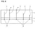
- FIG. 6 illustrates a schematic view showing a structure of a conventional group III nitride compound semiconductor.
- a buffer layer 2 and a group III nitride compound semiconductor layer 3 are formed successively on a substrate 1.
- the substrate 1 and the buffer layer 2 are made of sapphire and aluminum nitride (AlN), respectively.
- AlN buffer layer 2 is formed to relax misfit between the sapphire substrate 1 and the group III nitride compound semiconductor layer 3, possibility of generating dislocations cannot be 0.
- Feedthrough dislocations 4 are propagated from dislocation generating points 40 in longitudinal direction (a direction vertical to a surface of the substrate), penetrating the buffer layer 2 and the group III nitride compound semiconductor layer 3.
- manufacturing a semiconductor device by laminating various group III nitride compound semiconductor layers on the group III nitride compound semiconductor layer 3 results in propagating feedthrough dislocations 4 from dislocation generating points 41 which reach the surface of the group III nitride compound semiconductor layer 3, further through the semiconductor device in longitudinal direction. Accordingly, it had been difficult to prevent dislocations from propagating in the semiconductor device at the time when a group III nitride compound semiconductor layer is formed.
- an object of the present invention is to realize an efficient method capable of forming a layer of a group III nitride compound semiconductor without generation of cracks and dislocations to thereby improve device characteristics.
- the present invention has a first feature that resides in a method for manufacturing a group III nitride compound semiconductor, which hardly grows epitaxially on a substrate, by crystal growth, comprising: forming a buffer layer on a substrate into an island pattern such as a dot pattern, a striped pattern, or a grid pattern such that substrate-exposed portions are formed in a scattered manner; and forming a group III nitride compound semiconductor layer on the buffer layer by growing a group III nitride compound epitaxially in longitudinal and lateral directions.
- forming substrate-exposed portions in a scattered manner does not necessarily represent the condition that each substrate-exposed portions is completely separated, but represents the condition that the buffer layer exists around arbitrary substrate-exposed portions.
- the following method can be applied: forming the buffer layer on the entire surface of the substrate and then removing the desired portions of the buffer layer by etching; or forming a selective mask such as an SiO 2 film on the substrate and partially forming the buffer layer.
- the "lateral" direction as used in the specification refers to a direction parallel to a surface of the substrate.
- the group III nitride compound semiconductor grows on the buffer layer in a longitudinal direction.
- the group III nitride compound semiconductor which grows on the buffer layer in a longitudinal direction also grows in a lateral direction in order to cover the substrate-exposed portions.
- the growth velocity of the group III nitride compound semiconductor in the longitudinal and lateral directions can be controlled by conditions of, for example, temperature, pressure, or supplying conditions of source materials.
- a group III nitride compound semiconductor layer reunited into one layer can cover the substrate-exposed portions which are not covered by the buffer layer from a base of the buffer layer which is formed into an island pattern such as a dot pattern, a striped pattern or a grid pattern.
- feedthrough dislocations of the group III nitride compound semiconductor exists only in the regions of group III nitride compound semiconductor layer formed on the buffer layer, which is formed into an island pattern such as a dot pattern, a striped pattern or a grid pattern. This is because feedthrough dislocations are not generated when the group III nitride compound semiconductor grows in a lateral direction but are generated when it grows in a longitudinal direction.
- the second feature of the present invention is a method for manufacturing a group III nitride compound semiconductor, which hardly grows epitaxially on a substrate, by crystal growth, comprising: forming a buffer layer on a substrate into an island pattern such as a dot pattern, a striped pattern, or a grid pattern such that substrate-exposed portions are formed in a scattered manner; forming a group III nitride compound semiconductor layer on the buffer layer by growing a group III nitride compound epitaxially in longitudinal and lateral directions; etching at least one of the regions of the group III nitride compound semiconductor layer, growing in a longitudinal direction on the buffer layer which is formed into an island pattern; and growing the group III nitride compound semiconductor, which is left without being etched, in a lateral direction. Forming substrate-exposed portions in a scattered manner is explained in the first feature.
- the group III nitride compound semiconductor layer is etched after carrying out the method of the first feature, and then it is grown in a lateral direction in order to cover the etched regions.
- the surface density of longitudinal feedthrough dislocations of the group III nitride compound semiconductor layer decreases, and crystallinity of the device is thus improved.
- feedthrough dislocations generated by the longitudinal growth of the semiconductor layer can be eliminated. It is preferable to also etch the buffer layer to expose the substrate during etching of the group III nitride compound semiconductor layer.
- the substrate-exposed regions can be covered and a group III nitride compound semiconductor layer which is reunited into one layer can be obtained.
- the lateral growth can be promoted by the conditions of, for example, temperature, pressure, or supplying conditions of source materials.
- feedthrough dislocations existing in the group III nitride compound semiconductor layer can be eliminated.
- the group III nitride compound semiconductor layer does not have longitudinal feedthrough dislocations, and crystallinity of the device is, therefore, improved.
- the scope of the present invention also involves a method of etching regions of the group III nitride compound semiconductor layer, including the upper surface of the buffer layer, wider than the width of the buffer layer in case that feedthrough dislocations are generated partially inclined (in a lateral direction).
- all the regions of the group III nitride compound semiconductor layer which have feedthrough dislocations and grow on the buffer layer, which is formed into an island pattern such as a dot pattern, a striped pattern, or a grid pattern is not necessarily etched.
- the group III nitride compound semiconductor layer can be reunited into one layer by growing it in a lateral direction again, even when feedthrough dislocations are left without being etched in the semiconductor layer.
- the scope of the present invention also involves a method of dividing etching and epitaxial lateral overgrowth (ELO) components into several parts, according to a position or a design of the regions to form the buffer layer and limitations in the process afterward.
- ELO epitaxial lateral overgrowth
- the third feature of the present invention is to combine epitaxial growth of a group III nitride compound semiconductor layer formed on the buffer layer in longitudinal direction and epitaxial growth of the group III nitride compound in a lateral direction by using the difference between the velocities of epitaxial growth of the group III nitride compound semiconductor layer on the buffer layer and on the exposed substrate, in order to obtain a group III nitride compound semiconductor layer which covers the surface of the substrate.
- the difference between the velocities of epitaxial growth of the group III nitride compound semiconductor on the buffer layer and on the substrate can be easily controlled by the conditions of, for example, temperature, pressure, or supplying conditions of source materials.
- the velocities of growing the group III nitride compound semiconductor epitaxially on the buffer layer in longitudinal and lateral directions can be controlled. By controlling these conditions, surface density of feedthrough dislocations of the group III nitride compound semiconductor layer in longitudinal direction is decreased, and crystallinity of the device is improved.
- the difference between the velocities of epitaxial growth of the group III nitride compound semiconductor on the buffer layer and on the substrate is used.
- the group III nitride compound semiconductor comprises a compound which is identical to that of the buffer layer in view of stoichiometric composition.
- the compound of the group III nitride compound semiconductor can be non-crystalline, a set of micro-crystalline and polycrystalline, or single-crystalline.
- the difference between the velocities of epitaxial growth of the group III nitride compound semiconductor layer on the buffer layer and on the exposed substrate is an essential point of the present invention, and combination of the group III nitride compound, the compound forming the buffer layer, and materials to form the substrate is a method of generating the different epitaxial growth velocities.
- the fourth feature of the present invention is that the substrate is made of sapphire. As a result, it is difficult to epitaxially grow the group III nitride compound semiconductor on the substrate.
- the fifth feature of the present invention is that the buffer layer is made of aluminum nitride (AlN). And the sixth feature of the present invention is that the group III nitride compound semiconductor which grows in lateral direction does not comprise aluminum (Al).
- the seventh feature of the present invention is to obtain a light-emitting group III nitride compound semiconductor device by forming an another group III nitride compound semiconductor layer on the group III nitride compound semiconductor, which is formed on the region where the buffer layer is not formed, by using the above-described method. Because the group III nitride compound semiconductor layer is laminated on the regions which have no surface density of longitudinal feedthrough dislocations, reliability of the device is improved.
- the eighth feature of the present invention is to obtain only the group III nitride compound semiconductor layer by using the above-described method.
- the group III nitride compound semiconductor layer which is a layer laminated on the substrate, is left by removing the substrate. If necessary, the buffer layer can be removed with the substrate.
- the group III nitride compound semiconductor layer can dope an arbitrary dopant into the substrate so that the substrate has an arbitrary resistivity, and the group III nitride compound semiconductor layer with non-insulated substrate can be obtained. Because the group III nitride compound semiconductor layer has little or no surface density of feedthrough dislocations, it can be useful as a semiconductor substrate.
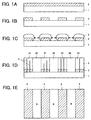
- FIGS. 1A-1E, 3A-3C, and 4A-4C each show views of processes for manufacturing a group III nitride compound semiconductor according to the first embodiment of the present invention.
- the group III nitride compound semiconductor of the present invention is formed through the use of a metal organic vapor phase epitaxy (hereinafter referred to as "MOVPE") method.
- Gases used in the MOVPE method are ammonia (NH 3 ), carrier gas (H 2 , or N 2 ), trimethyl gallium (Ga(CH 3 ) 3 ) (hereinafter referred to as "TMG”), and trimethyl aluminum (Al(CH 3 ) 3 ) (hereinafter referred to as "TMA").
- a single crystalline sapphire substrate 1 is formed to have a main surface 'a' which is cleaned by an organic washing solvent and heat treatment.
- An AlN buffer layer 2, having a thickness of about 40nm, is then formed on the surface 'a' of the sapphire substrate 1 under conditions controlled by lowering the temperature to 400°C and concurrently supplying H 2 , NH 3 and TMA at a flow rate of 10L/min, 5L/min, and 20 ⁇ mol/min, respectively, for 3 minutes (FIG. 1A).
- the buffer layer 2 is then dry-etched in a striped pattern by selective dry-etching including reactive ion etching (RIE) using a hard baked resist mask.
- RIE reactive ion etching
- the AlN buffer layer 2 is formed in a striped pattern such that each region defined above the buffer layer 2, has a width of 5 ⁇ m, and each region where the sapphire substrate 1 was exposed, has a width of 5 ⁇ m, and are formed alternately (FIGS. 1B and 1E).
- GaN layer 3 having a thickness of several thousands ⁇ was grown to cover the entire surface of the substrate and the AlN buffer layer, while maintaining the substrate 1 at a temperature of 1150°C, and feeding H 2 , NH 3 and TMG at 20L/min, 10L/min and 5 ⁇ mol/min, respectively. TMG is then fed at 300 ⁇ mol/min, thereby obtaining about 3 ⁇ m in thickness of GaN layer 3 at a growth temperature of 1000°C.
- the GaN layer 3 was formed by growing GaN regions 32 epitaxially on the sapphire substrate 1 in a lateral direction, from the GaN regions 31 which grows epitaxially on the upper surface of the AlN buffer layer 2 in a longitudinal direction and serves as a nucleus (FIGS. 1C and 1D). Accordingly, GaN regions 32 having excellent crystallinity can be obtained on the regions where the AlN buffer layer 2 is not formed and the sapphire substrate 1 is exposed.
- a group III nitride compound semiconductor device can be formed using the GaN regions 32 having excellent crystallinity, which is formed by epitaxial lateral overgrowth (ELO) method on the upper surface of the sapphire substrate 1, where predetermined regions of the substrate 1 for forming the device are exposed.
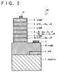
- FIG. 2 illustrates a device 100 comprising an LD formed on the GaN regions of high crystallinity in a Si-doped n-type GaN layer 30.
- the n-GaN regions of high crystallinity is formed in the regions where the AlN buffer layer is not formed, and the following layers are laminated in sequence on each of the regions: an n-Al 0.07 Ga 0.93 N cladding layer 4c; an n-GaN guide layer 5; an emission layer 6 having a multiple quantum well (MQW) structure, in which a well layer 61 made of Ga 0.9 In 0.1 N and a barrier layer 62 made of Ga 0.97 In 0.03 N were laminated alternately; a p-GaN guide layer 7; a p-Al 0.07 Ga 0.93 N cladding layer 8; and a p-GaN contact layer 9.
- MQW multiple quantum well
- electrodes 11 and 10 are formed on the n-GaN layer 30 and the p-GaN contact layer 9, respectively. Because the LD shown in FIG. 2 does not have feedthrough dislocations except around the electrode 11, reliability of the LD as a device is improved.
- a single crystalline sapphire substrate 1 is formed to have a main surface 'a' which is cleaned by an organic washing solvent and heat treatment.
- An AlN buffer layer 2, having a thickness of about 40nm is then formed on the surface 'a' of the sapphire substrate 1 under conditions controlled by lowering the temperature to 400°C and concurrently supplying H 2 , NH 3 and TMA at a flow rate of 10L/min, 5L/min, and 20 ⁇ mol/min, respectively, for 3 minutes.
- the buffer layer 2 is dry-etched in a striped pattern by selective dry-etching including reactive ion etching (RIE) using a hard baked resist mask.
- RIE reactive ion etching
- the AlN buffer layer 2 is formed in a striped pattern such that each region defined above the buffer layer 2, has a width of 5 ⁇ m, and each region where the sapphire substrate 1 is exposed, has a width of 5 ⁇ m, and are formed alternately.
- a GaN layer 3 having a thickness of several thousands ⁇ is grown to cover the entire surface of the substrate and the AlN buffer layer, while maintaining the substrate 1 at a temperature of 1150°C, and feeding H 2 , NH 3 and TMG were fed at 20L/min, 10L/min and 5 ⁇ mol/min, respectively. TMG is then fed at 300 ⁇ mol/min, thereby obtaining about 3 ⁇ m in thickness of GaN layer 3 at a growth temperature of 1000°C.
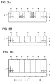
- the GaN layer 3 is formed by growing GaN regions 32 epitaxially on the sapphire substrate 1 in a lateral direction, from the GaN regions 31 which grow epitaxially on the upper surface of the AlN buffer layer 2 in a longitudinal direction and serves as a nucleus (FIG. 3A).
- the GaN regions 31 which grow epitaxially on the upper surface of the AlN buffer layer 2 in a longitudinal direction is dry-etched by selective etching (FIG. 3B).
- AlN buffer layer 2 is also etched.
- a film 3 having a thickness of several thousands ⁇ is formed to cover the entire surface of the group III nitride compound semiconductor, while maintaining the substrate 1 at a temperature of 1150°C, and feeding H 2 , NH 3 and TMG at 20L/min, 10L/min and 5 ⁇ mol/min, respectively. TMG is then fed at 300 ⁇ mol/min, thereby obtaining about 3 ⁇ m in thickness of GaN layer 3 at a growth temperature of 1000°C.
- GaN region 32 and GaN region 33 both have high crystallinity, and are formed on the sapphire substrate 1.
- the GaN region 32 is formed on the sapphire substrate 1 which is exposed by dry-etching the AlN buffer layer 2.
- the GaN region 33 is formed on the sapphire substrate 1 which is exposed by dry-etching the GaN regions 31 and the AlN buffer layer 2.
- a GaN layer 3 which has excellent crystallinity and does not have feedthrough dislocations, can be formed over a wide area W as shown in FIG. 3C.
- FIGS. 4A-4C are plan views of FIGS. 3A-3C.
- a GaN layer of excellent crystallinity is formed on a region other than a portion where the GaN region 31, which grows epitaxially on the upper surface of the AlN buffer layer 2 in a longitudinal direction, are formed.
- FIG. 4A illustrates the buffer layer 2 which is formed in a striped pattern. Regions represented by B are where the sapphire substrate 1 is exposed.
- FIG. 4B shows the GaN layer 3 left after etching the GaN region 31 and the buffer layer 2 thereunder, which grows epitaxially on the buffer layer 2 in a longitudinal direction. As shown in FIG. 4B, the GaN region 31 which has feedthrough dislocations is left at both sides of the substrate in order to support the GaN regions 32 of higher crystallinity, thus, preventing the GaN region 32 from peeling.
- FIG. 4C shows the GaN layer 3 reunited into one layer by epitaxial lateral overgrowth (ELO). As shown in FIG. 4C, the GaN layer 3 comprises GaN regions 31, 32 and 33.
- ELO epitaxial lateral overgrowth
- the GaN region 31 is formed on the buffer layer 2 and has feedthrough dislocations.
- the GaN region 32 is formed on the exposed substrate 1 and has no feedthrough dislocations.
- the GaN region 33 is formed after removing the buffer layer 2 and the GaN layer 31 and has no feedthrough dislocations. Accordingly, the crystallinity of GaN regions 32 and 33, or a region W, which has no feedthrough dislocations, is very desirable.
- the sapphire substrate 1 and the buffer layer 2 are removed by machinery polishing and then the GaN region 31 which has feedthrough dislocations and is at both side of the substrate is cut.
- the width of the regions defined above the AlN buffer layer 2, which are formed in a striped pattern is 5 ⁇ m
- a preferred range for the width is from 1 ⁇ m to 10 ⁇ m. This is because when the width of the regions becomes larger than 10 ⁇ m, the probability of generating dislocations increases. When the width of the regions becomes smaller than 1 ⁇ m, obtaining a GaN layer 3 with wide area and high quality becomes difficult.
- a width b of the regions B where the substrate 1 is exposed has a width of about 5 ⁇ m, a preferred range for the width is from 1 ⁇ m to 10 ⁇ m.
- a preferred range for thickness of the n-layer 3 made of GaN is 50 ⁇ m to 100 ⁇ m, because the n-layer 3 can be formed without dislocations.
- the buffer layer 2 and the group III nitride compound semiconductor layer 3 comprise aluminum nitride (AlN) and gallium nitride (GaN), respectively. Alternatively, these materials are not limited to AlN and GaN, respectively.
- An essential point of the present invention is to grow the group III nitride compound semiconductor, which does not grow epitaxially on the substrate, on the buffer layer epitaxially in a longitudinal direction and on the exposed substrate portion in a lateral direction, in order to form regions without feedthrough dislocations.
- the materials of the substrate, the buffer layer, and the composition ratio of the group III nitride compound semiconductor can be combined in different ways in accordance with different conditions for epitaxial growth.
- sapphire is used to form the substrate 1.
- silicon Si
- silicon carbide SiC
- other materials can be used.
- aluminum nitride is used to form the buffer layer 2.
- gallium nitride (GaN), gallium indium nitride (Ga x In 1-x N, 0 ⁇ x ⁇ 1), aluminum gallium nitride (Al x Ga 1-x N, 0 ⁇ x ⁇ 1) or aluminum gallium indium nitride (Al x Ga y In 1-x-y N, 0 ⁇ x ⁇ 1, 0 ⁇ y ⁇ 1, 0 ⁇ x+y ⁇ 1) may also be used.
- the buffer layer 2 is formed in a striped pattern.
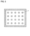
- the buffer layer 2 can be formed into an island pattern by exposing the substrate 1 in a grid pattern as shown in FIG. 5.
- the buffer layer 2 surrounds the peripheral surface of the substrate in FIG. 5, it is not necessarily present.
- a group III nitride compound semiconductor substrate can be obtained. Except when selectivity of epitaxial growth is prevented, an arbitrary dopant such as silicon (Si), germanium (Ge), zinc (Zn), indium (In), or magnesium (Mg) may be doped into the group III nitride compound semiconductor substrate. Accordingly, the group III nitride compound semiconductor substrate which has an arbitrary resistivity and includes an arbitrary dopant may be obtained.
- a light-emitting diode or a laser device comprising various group III nitride compound semiconductors, which is well known to have a double hetero structure comprising a guide layer, a cladding layer, an active layer having an MQW or SQW structure can be formed in the group III nitride compound semiconductor substrate of the present invention.
- a resonator facet can be easily cleaved because all the layers from the substrate to other layers are made of group III nitride compound semiconductors. As a result, oscillation efficiency of the laser can be improved.
- the group III nitride compound semiconductor substrate to have conductivity, electric current can flow in a vertical direction to the surface of the substrate.
- a process for forming an electrode can be simplified and the sectional area of the current path becomes wider and the length becomes shorter, resulting in lowering a driving voltage of the device.
- the MOVPE method is carried out under normal pressure.
- the MOVPE method can be carried out under reduced pressure. Further alternatively, it can be carried out under conditions combining normal pressure and reduced pressure.
- the group III nitride compound semiconductor of the present invention can be applied not only to a light-emitting device such as an LED or an LD but also to a light-receiving device or an electronic device.
- a buffer layer 2 made of aluminum nitride (AlN) is formed on a substrate 1 and is formed into an island pattern such as a dot pattern, a striped pattern, or a grid pattern such that substrate-exposed portions are formed in a scattered manner.
- a group III nitride compound semiconductor 3 grows epitaxially on the buffer layer 2 in a longitudinal direction, and grows epitaxially on the substrate-exposed portions in a lateral direction. As a result, a group III nitride compound semiconductor 3 which has little or no feedthrough dislocations 4 is obtained.
- region 32 Because the region where the group III nitride compound semiconductor 3 grows epitaxially in a lateral direction, on region 32, has excellent crystallinity, forming a group III nitride compound semiconductor device on the upper surface of the region results in improved device characteristics.
Abstract
A buffer layer 2 made of aluminum nitride (AlN) is
formed on a substrate 1 and is formed into an island pattern
such as a dot pattern, a striped pattern, or a grid pattern
such that substrate-exposed portions are formed in a
scattered manner. A group III nitride compound
semiconductor 3 grows epitaxially on the buffer layer 2 in a
longitudinal direction, and grows epitaxially on the
substrate-exposed portions in a lateral direction. As a
result, a group III nitride compound semiconductor 3 which
has little or no feedthrough dislocations 4 is obtained.
Because the region where the group III nitride compound
semiconductor 3 grows epitaxially in a lateral direction, on
region 32, has excellent crystallinity, forming a group III
nitride compound semiconductor device on the upper surface
of the region results in improved device characteristics.
Description
The present invention relates to a method for
manufacturing a group III nitride compound semiconductor.
Especially, the present invention relates to a method for
manufacturing a group III nitride compound semiconductor in
which an epitaxial lateral overgrowth (ELO) method is used
to form a layer on a substrate. The present invention also
relates to a light-emitting device using a group III nitride
compound semiconductor formed on a group III nitride
compound semiconductor layer using the ELO method. A group
III nitride compound semiconductor can be made of binary
compounds such as AlN, GaN or InN, ternary compounds such as
AlxGa1-xN, AlxIn1-xN or GaxIn1-xN (0<x<1), or quaternary
compounds AlxGayIn1-x-yN (0<x<1, 0<y<1, 0<x+y<1), that is,
those are represented by a general formula AlxGayIn1-x-yN
(0≤x≤1, 0≤y≤1, 0≤x+y≤1).
A group III nitride compound semiconductor is a direct-transition-type
semiconductor having a wide emission
spectrum range from ultraviolet to red, and is applied to
light-emitting devices such as light-emitting diodes (LEDs)
and laser diodes (LDs). The group III nitride compound
semiconductor is, in general, formed on a sapphire substrate.
However, in the above-described conventional technique,
when a layer of a group III nitride compound semiconductor
is formed on a sapphire substrate, cracks and/or warpage are
generated in the semiconductor layer due to a difference in
thermal expansion coefficient between sapphire and the group
III nitride compound semiconductor, and dislocations are
generated in the semiconductor layer due to misfit, which
result in degraded device characteristics. Especially,
dislocations due to misfit are feedthrough dislocations
which penetrate the semiconductor layer in longitudinal
direction, resulting in propagation of about 109 cm-2 of
dislocation in the group III nitride compound semiconductor.
FIG. 6 illustrates a schematic view showing a structure
of a conventional group III nitride compound semiconductor.
In FIG. 6, a buffer layer 2 and a group III nitride compound
semiconductor layer 3 are formed successively on a substrate
1. In general, the substrate 1 and the buffer layer 2 are
made of sapphire and aluminum nitride (AlN), respectively.
Although the AlN buffer layer 2 is formed to relax misfit
between the sapphire substrate 1 and the group III nitride
compound semiconductor layer 3, possibility of generating
dislocations cannot be 0. Feedthrough dislocations 4 are
propagated from dislocation generating points 40 in
longitudinal direction (a direction vertical to a surface of
the substrate), penetrating the buffer layer 2 and the group
III nitride compound semiconductor layer 3. Thus,
manufacturing a semiconductor device by laminating various
group III nitride compound semiconductor layers on the group
III nitride compound semiconductor layer 3 results in
propagating feedthrough dislocations 4 from dislocation
generating points 41 which reach the surface of the group
III nitride compound semiconductor layer 3, further through
the semiconductor device in longitudinal direction.
Accordingly, it had been difficult to prevent dislocations
from propagating in the semiconductor device at the time
when a group III nitride compound semiconductor layer is
formed.
Accordingly, in light of the above problems, an object
of the present invention is to realize an efficient method
capable of forming a layer of a group III nitride compound
semiconductor without generation of cracks and dislocations
to thereby improve device characteristics.
In order to solve the above problems, the present
invention has a first feature that resides in a method for
manufacturing a group III nitride compound semiconductor,
which hardly grows epitaxially on a substrate, by crystal
growth, comprising: forming a buffer layer on a substrate
into an island pattern such as a dot pattern, a striped
pattern, or a grid pattern such that substrate-exposed
portions are formed in a scattered manner; and forming a
group III nitride compound semiconductor layer on the buffer
layer by growing a group III nitride compound epitaxially in
longitudinal and lateral directions.
Here forming substrate-exposed portions in a scattered
manner does not necessarily represent the condition that
each substrate-exposed portions is completely separated, but
represents the condition that the buffer layer exists around
arbitrary substrate-exposed portions. In order to form the
buffer layer into an island pattern such as a dot pattern, a
striped pattern or a grid pattern, the following method can
be applied: forming the buffer layer on the entire surface
of the substrate and then removing the desired portions of
the buffer layer by etching; or forming a selective mask
such as an SiO2 film on the substrate and partially forming
the buffer layer.
The "lateral" direction as used in the specification
refers to a direction parallel to a surface of the substrate.
By using the above-described method, the group III nitride
compound semiconductor grows on the buffer layer in a
longitudinal direction. The group III nitride compound
semiconductor which grows on the buffer layer in a
longitudinal direction also grows in a lateral direction in
order to cover the substrate-exposed portions. The growth
velocity of the group III nitride compound semiconductor in
the longitudinal and lateral directions can be controlled by
conditions of, for example, temperature, pressure, or
supplying conditions of source materials. Accordingly, a
group III nitride compound semiconductor layer reunited into
one layer can cover the substrate-exposed portions which are
not covered by the buffer layer from a base of the buffer
layer which is formed into an island pattern such as a dot
pattern, a striped pattern or a grid pattern. As a result,
feedthrough dislocations of the group III nitride compound
semiconductor exists only in the regions of group III
nitride compound semiconductor layer formed on the buffer
layer, which is formed into an island pattern such as a dot
pattern, a striped pattern or a grid pattern. This is
because feedthrough dislocations are not generated when the
group III nitride compound semiconductor grows in a lateral
direction but are generated when it grows in a longitudinal
direction. Accordingly, surface density of longitudinal
feedthrough dislocations of the group III nitride compound
semiconductor layer decreases, and crystallinity of the
device is improved. When a group III nitride compound
semiconductor device which is manufactured using only a
group III nitride compound semiconductor layer which is
formed on the substrate-exposed portions, or the regions
which are not covered by a buffer layer, surface density of
feedthrough dislocations of the device can become 0.
The second feature of the present invention is a method
for manufacturing a group III nitride compound semiconductor,
which hardly grows epitaxially on a substrate, by crystal
growth, comprising: forming a buffer layer on a substrate
into an island pattern such as a dot pattern, a striped
pattern, or a grid pattern such that substrate-exposed
portions are formed in a scattered manner; forming a group
III nitride compound semiconductor layer on the buffer layer
by growing a group III nitride compound epitaxially in
longitudinal and lateral directions; etching at least one of
the regions of the group III nitride compound semiconductor
layer, growing in a longitudinal direction on the buffer
layer which is formed into an island pattern; and growing
the group III nitride compound semiconductor, which is left
without being etched, in a lateral direction. Forming
substrate-exposed portions in a scattered manner is
explained in the first feature.
In the second feature of the present invention, the
group III nitride compound semiconductor layer is etched
after carrying out the method of the first feature, and then
it is grown in a lateral direction in order to cover the
etched regions. As described in the first feature of the
present invention, the surface density of longitudinal
feedthrough dislocations of the group III nitride compound
semiconductor layer decreases, and crystallinity of the
device is thus improved. By etching the regions of the
group III nitride compound semiconductor layer which grow on
the buffer layer in a longitudinal direction and have
feedthrough dislocations, feedthrough dislocations generated
by the longitudinal growth of the semiconductor layer can be
eliminated. It is preferable to also etch the buffer layer
to expose the substrate during etching of the group III
nitride compound semiconductor layer.
By growing the group III nitride compound semiconductor
in a lateral direction again, the substrate-exposed regions
can be covered and a group III nitride compound
semiconductor layer which is reunited into one layer can be
obtained. The lateral growth can be promoted by the
conditions of, for example, temperature, pressure, or
supplying conditions of source materials. As a result,
feedthrough dislocations existing in the group III nitride
compound semiconductor layer can be eliminated. Thus, the
group III nitride compound semiconductor layer does not have
longitudinal feedthrough dislocations, and crystallinity of
the device is, therefore, improved. The scope of the
present invention also involves a method of etching regions
of the group III nitride compound semiconductor layer,
including the upper surface of the buffer layer, wider than
the width of the buffer layer in case that feedthrough
dislocations are generated partially inclined (in a lateral
direction). Similarly, all the regions of the group III
nitride compound semiconductor layer which have feedthrough
dislocations and grow on the buffer layer, which is formed
into an island pattern such as a dot pattern, a striped
pattern, or a grid pattern, is not necessarily etched. The
group III nitride compound semiconductor layer can be
reunited into one layer by growing it in a lateral direction
again, even when feedthrough dislocations are left without
being etched in the semiconductor layer. The scope of the
present invention also involves a method of dividing etching
and epitaxial lateral overgrowth (ELO) components into
several parts, according to a position or a design of the
regions to form the buffer layer and limitations in the
process afterward.
The third feature of the present invention is to
combine epitaxial growth of a group III nitride compound
semiconductor layer formed on the buffer layer in
longitudinal direction and epitaxial growth of the group III
nitride compound in a lateral direction by using the
difference between the velocities of epitaxial growth of the
group III nitride compound semiconductor layer on the buffer
layer and on the exposed substrate, in order to obtain a
group III nitride compound semiconductor layer which covers
the surface of the substrate. The difference between the
velocities of epitaxial growth of the group III nitride
compound semiconductor on the buffer layer and on the
substrate can be easily controlled by the conditions of, for
example, temperature, pressure, or supplying conditions of
source materials. Similarly, the velocities of growing the
group III nitride compound semiconductor epitaxially on the
buffer layer in longitudinal and lateral directions can be
controlled. By controlling these conditions, surface
density of feedthrough dislocations of the group III nitride
compound semiconductor layer in longitudinal direction is
decreased, and crystallinity of the device is improved.
In this feature, the difference between the velocities
of epitaxial growth of the group III nitride compound
semiconductor on the buffer layer and on the substrate is
used. But this does not necessarily exclude the possibility
that the group III nitride compound semiconductor comprises
a compound which is identical to that of the buffer layer in
view of stoichiometric composition. Depending on the layer
formed under the semiconductor layer and the condition of
the epitaxial growth, the compound of the group III nitride
compound semiconductor can be non-crystalline, a set of
micro-crystalline and polycrystalline, or single-crystalline.
The difference between the velocities of epitaxial growth of
the group III nitride compound semiconductor layer on the
buffer layer and on the exposed substrate is an essential
point of the present invention, and combination of the group
III nitride compound, the compound forming the buffer layer,
and materials to form the substrate is a method of
generating the different epitaxial growth velocities.
The fourth feature of the present invention is that the
substrate is made of sapphire. As a result, it is difficult
to epitaxially grow the group III nitride compound
semiconductor on the substrate.
The fifth feature of the present invention is that the
buffer layer is made of aluminum nitride (AlN). And the
sixth feature of the present invention is that the group III
nitride compound semiconductor which grows in lateral
direction does not comprise aluminum (Al).
The seventh feature of the present invention is to
obtain a light-emitting group III nitride compound
semiconductor device by forming an another group III nitride
compound semiconductor layer on the group III nitride
compound semiconductor, which is formed on the region where
the buffer layer is not formed, by using the above-described
method. Because the group III nitride compound
semiconductor layer is laminated on the regions which have
no surface density of longitudinal feedthrough dislocations,
reliability of the device is improved.
The eighth feature of the present invention is to
obtain only the group III nitride compound semiconductor
layer by using the above-described method. The group III
nitride compound semiconductor layer, which is a layer
laminated on the substrate, is left by removing the
substrate. If necessary, the buffer layer can be removed
with the substrate. When an insulator is used to form the
substrate, the group III nitride compound semiconductor
layer can dope an arbitrary dopant into the substrate so
that the substrate has an arbitrary resistivity, and the
group III nitride compound semiconductor layer with non-insulated
substrate can be obtained. Because the group III
nitride compound semiconductor layer has little or no
surface density of feedthrough dislocations, it can be
useful as a semiconductor substrate.
The present invention will now be described by way of
concrete embodiments.
FIGS. 1A-1E, 3A-3C, and 4A-4C each show views of
processes for manufacturing a group III nitride compound
semiconductor according to the first embodiment of the
present invention. The group III nitride compound
semiconductor of the present invention is formed through the
use of a metal organic vapor phase epitaxy (hereinafter
referred to as "MOVPE") method. Gases used in the MOVPE
method are ammonia (NH3), carrier gas (H2, or N2), trimethyl
gallium (Ga(CH3)3) (hereinafter referred to as "TMG"), and
trimethyl aluminum (Al(CH3)3) (hereinafter referred to as
"TMA").
A single crystalline sapphire substrate 1 is formed to
have a main surface 'a' which is cleaned by an organic
washing solvent and heat treatment. An AlN buffer layer 2,
having a thickness of about 40nm, is then formed on the
surface 'a' of the sapphire substrate 1 under conditions
controlled by lowering the temperature to 400°C and
concurrently supplying H2, NH3 and TMA at a flow rate of
10L/min, 5L/min, and 20µmol/min, respectively, for 3
minutes (FIG. 1A). The buffer layer 2 is then dry-etched in
a striped pattern by selective dry-etching including
reactive ion etching (RIE) using a hard baked resist mask.
Accordingly, the AlN buffer layer 2 is formed in a striped
pattern such that each region defined above the buffer layer
2, has a width of 5µm, and each region where the sapphire
substrate 1 was exposed, has a width of 5µm, and are formed
alternately (FIGS. 1B and 1E).
A GaN layer 3 having a thickness of several thousands Å
was grown to cover the entire surface of the substrate and
the AlN buffer layer, while maintaining the substrate 1 at a
temperature of 1150°C, and feeding H2, NH3 and TMG at
20L/min, 10L/min and 5µmol/min, respectively. TMG is then
fed at 300µmol/min, thereby obtaining about 3µm in
thickness of GaN layer 3 at a growth temperature of 1000°C.
In this embodiment, the GaN layer 3 was formed by growing
GaN regions 32 epitaxially on the sapphire substrate 1 in a
lateral direction, from the GaN regions 31 which grows
epitaxially on the upper surface of the AlN buffer layer 2
in a longitudinal direction and serves as a nucleus (FIGS.
1C and 1D). Accordingly, GaN regions 32 having excellent
crystallinity can be obtained on the regions where the AlN
buffer layer 2 is not formed and the sapphire substrate 1 is
exposed.
A group III nitride compound semiconductor device can
be formed using the GaN regions 32 having excellent
crystallinity, which is formed by epitaxial lateral
overgrowth (ELO) method on the upper surface of the sapphire
substrate 1, where predetermined regions of the substrate 1
for forming the device are exposed. FIG. 2 illustrates a
device 100 comprising an LD formed on the GaN regions of
high crystallinity in a Si-doped n-type GaN layer 30. The
n-GaN regions of high crystallinity is formed in the regions
where the AlN buffer layer is not formed, and the following
layers are laminated in sequence on each of the regions: an
n-Al0.07Ga0.93N cladding layer 4c; an n-GaN guide layer 5; an
emission layer 6 having a multiple quantum well (MQW)
structure, in which a well layer 61 made of Ga0.9In0.1N and a
barrier layer 62 made of Ga0.97In0.03N were laminated
alternately; a p-GaN guide layer 7; a p-Al0.07Ga0.93 N cladding
layer 8; and a p-GaN contact layer 9. Then electrodes 11
and 10 are formed on the n-GaN layer 30 and the p-GaN
contact layer 9, respectively. Because the LD shown in FIG.
2 does not have feedthrough dislocations except around the
electrode 11, reliability of the LD as a device is improved.
A single crystalline sapphire substrate 1 is formed to
have a main surface 'a' which is cleaned by an organic
washing solvent and heat treatment. An AlN buffer layer 2,
having a thickness of about 40nm is then formed on the
surface 'a' of the sapphire substrate 1 under conditions
controlled by lowering the temperature to 400°C and
concurrently supplying H2, NH3 and TMA at a flow rate of
10L/min, 5L/min, and 20µmol/min, respectively, for 3
minutes. The buffer layer 2 is dry-etched in a striped
pattern by selective dry-etching including reactive ion
etching (RIE) using a hard baked resist mask. Accordingly,
the AlN buffer layer 2 is formed in a striped pattern such
that each region defined above the buffer layer 2, has a
width of 5µm, and each region where the sapphire substrate
1 is exposed, has a width of 5µm, and are formed
alternately.
A GaN layer 3 having a thickness of several thousands Å
is grown to cover the entire surface of the substrate and
the AlN buffer layer, while maintaining the substrate 1 at a
temperature of 1150°C, and feeding H2, NH3 and TMG were fed
at 20L/min, 10L/min and 5µmol/min, respectively. TMG is
then fed at 300µmol/min, thereby obtaining about 3µm in
thickness of GaN layer 3 at a growth temperature of 1000°C.
In this embodiment, the GaN layer 3 is formed by growing GaN
regions 32 epitaxially on the sapphire substrate 1 in a
lateral direction, from the GaN regions 31 which grow
epitaxially on the upper surface of the AlN buffer layer 2
in a longitudinal direction and serves as a nucleus (FIG.
3A).
The GaN regions 31 which grow epitaxially on the upper
surface of the AlN buffer layer 2 in a longitudinal
direction is dry-etched by selective etching (FIG. 3B). In
this embodiment, AlN buffer layer 2 is also etched. A film
3 having a thickness of several thousands Å is formed to
cover the entire surface of the group III nitride compound
semiconductor, while maintaining the substrate 1 at a
temperature of 1150°C, and feeding H2, NH3 and TMG at
20L/min, 10L/min and 5µmol/min, respectively. TMG is then
fed at 300µmol/min, thereby obtaining about 3µm in
thickness of GaN layer 3 at a growth temperature of 1000°C.
TMG is then fed to the device at 300µmol/min, wherein each
space where the GaN region 31 is removed is covered again by
growing a region 33 in a lateral direction at a growth
temperature of 1000°C, and the GaN layer 3 is obtained
having a thickness about 3µm (FIG. 3C). Accordingly, GaN
region 32 and GaN region 33, both have high crystallinity,
and are formed on the sapphire substrate 1. The GaN region
32 is formed on the sapphire substrate 1 which is exposed by
dry-etching the AlN buffer layer 2. The GaN region 33 is
formed on the sapphire substrate 1 which is exposed by dry-etching
the GaN regions 31 and the AlN buffer layer 2. As a
result, a GaN layer 3, which has excellent crystallinity and
does not have feedthrough dislocations, can be formed over a
wide area W as shown in FIG. 3C.
FIGS. 4A-4C are plan views of FIGS. 3A-3C. In this
embodiment, a GaN layer of excellent crystallinity is formed
on a region other than a portion where the GaN region 31,
which grows epitaxially on the upper surface of the AlN
buffer layer 2 in a longitudinal direction, are formed.
FIG. 4A illustrates the buffer layer 2 which is formed
in a striped pattern. Regions represented by B are where
the sapphire substrate 1 is exposed. FIG. 4B shows the GaN
layer 3 left after etching the GaN region 31 and the buffer
layer 2 thereunder, which grows epitaxially on the buffer
layer 2 in a longitudinal direction. As shown in FIG. 4B,
the GaN region 31 which has feedthrough dislocations is left
at both sides of the substrate in order to support the GaN
regions 32 of higher crystallinity, thus, preventing the GaN
region 32 from peeling. FIG. 4C shows the GaN layer 3
reunited into one layer by epitaxial lateral overgrowth
(ELO). As shown in FIG. 4C, the GaN layer 3 comprises GaN
regions 31, 32 and 33. The GaN region 31 is formed on the
buffer layer 2 and has feedthrough dislocations. The GaN
region 32 is formed on the exposed substrate 1 and has no
feedthrough dislocations. The GaN region 33 is formed after
removing the buffer layer 2 and the GaN layer 31 and has no
feedthrough dislocations. Accordingly, the crystallinity of
GaN regions 32 and 33, or a region W, which has no
feedthrough dislocations, is very desirable.
After the above-described process, the sapphire
substrate 1 and the buffer layer 2 are removed by machinery
polishing and then the GaN region 31 which has feedthrough
dislocations and is at both side of the substrate is cut.
As a result, a group III nitride compound semiconductor
substrate of excellent crystallinity, comprising the GaN
layer 3 which has no feedthrough dislocations, is obtained.
Although the width of the regions defined above the AlN
buffer layer 2, which are formed in a striped pattern, is 5
µm, a preferred range for the width is from 1µm to 10µm.
This is because when the width of the regions becomes larger
than 10µm, the probability of generating dislocations
increases. When the width of the regions becomes smaller
than 1µm, obtaining a GaN layer 3 with wide area and high
quality becomes difficult. Additionally, although a width b
of the regions B where the substrate 1 is exposed has a
width of about 5µm, a preferred range for the width is from
1µm to 10µm. This is because when the width of the regions
B becomes larger than 10µm, a longer time is required for
lateral growth, and when the width of the regions B becomes
smaller than 1µm, the crystallinity of the GaN region 32
becomes too small. Further, in view of the crystallinity of
the n-layer 3 made of GaN, the ratio of the width a of the
region which is defined above the AlN buffer layer 2 to the
width b of the region B where the sapphire substrate 1 is
exposed; i.e., a/b, preferably falls within the range of 1
to 10.
In the above embodiments, a preferred range for
thickness of the n-layer 3 made of GaN is 50µm to 100µm,
because the n-layer 3 can be formed without dislocations.
In the present embodiment, the buffer layer 2 and the
group III nitride compound semiconductor layer 3 comprise
aluminum nitride (AlN) and gallium nitride (GaN),
respectively. Alternatively, these materials are not
limited to AlN and GaN, respectively. An essential point of
the present invention is to grow the group III nitride
compound semiconductor, which does not grow epitaxially on
the substrate, on the buffer layer epitaxially in a
longitudinal direction and on the exposed substrate portion
in a lateral direction, in order to form regions without
feedthrough dislocations. The materials of the substrate,
the buffer layer, and the composition ratio of the group III
nitride compound semiconductor can be combined in different
ways in accordance with different conditions for epitaxial
growth. Accordingly, when sapphire and aluminum nitride
(AlN) are used to form the substrate and the buffer layer,
respectively, a group III nitride compound semiconductor
represented by a general formula AlxGayIn1-x-yN (0≤x≤1, 0≤y≤1,
0≤x+y≤1, except AlN, when x=1 and y=0) and having an
arbitrary composition ratio may be used to form the group
III nitride compound semiconductor.
In the above embodiments, sapphire is used to form the
substrate 1. Alternatively, silicon (Si), silicon carbide
(SiC), and other materials can be used.
In the embodiments, aluminum nitride (AlN) is used to
form the buffer layer 2. Alternatively, gallium nitride
(GaN), gallium indium nitride (GaxIn1-xN, 0<x<1), aluminum
gallium nitride (AlxGa1-xN, 0<x<1) or aluminum gallium indium
nitride (AlxGayIn1-x-yN, 0<x<1, 0<y<1, 0<x+y<1) may also be
used.
In the embodiments, the buffer layer 2 is formed in a
striped pattern. Alternatively, the buffer layer 2 can be
formed into an island pattern by exposing the substrate 1 in
a grid pattern as shown in FIG. 5. Although the buffer
layer 2 surrounds the peripheral surface of the substrate in
FIG. 5, it is not necessarily present.
As described above, a group III nitride compound
semiconductor substrate can be obtained. Except when
selectivity of epitaxial growth is prevented, an arbitrary
dopant such as silicon (Si), germanium (Ge), zinc (Zn),
indium (In), or magnesium (Mg) may be doped into the group
III nitride compound semiconductor substrate. Accordingly,
the group III nitride compound semiconductor substrate which
has an arbitrary resistivity and includes an arbitrary
dopant may be obtained.
A light-emitting diode or a laser device comprising
various group III nitride compound semiconductors, which is
well known to have a double hetero structure comprising a
guide layer, a cladding layer, an active layer having an MQW
or SQW structure can be formed in the group III nitride
compound semiconductor substrate of the present invention.
For example, when a laser diode is formed on the group III
nitride compound semiconductor substrate, a resonator facet
can be easily cleaved because all the layers from the
substrate to other layers are made of group III nitride
compound semiconductors. As a result, oscillation
efficiency of the laser can be improved. And by forming the
group III nitride compound semiconductor substrate to have
conductivity, electric current can flow in a vertical
direction to the surface of the substrate. As a result, a
process for forming an electrode can be simplified and the
sectional area of the current path becomes wider and the
length becomes shorter, resulting in lowering a driving
voltage of the device.
In the above embodiments, the MOVPE method is carried
out under normal pressure. Alternatively, the MOVPE method
can be carried out under reduced pressure. Further
alternatively, it can be carried out under conditions
combining normal pressure and reduced pressure. The group
III nitride compound semiconductor of the present invention
can be applied not only to a light-emitting device such as
an LED or an LD but also to a light-receiving device or an
electronic device.
While the invention has been described in connection
with what are presently considered to be the most practical
and preferred embodiments, it is to be understood that the
invention is not to be limited to the disclosed embodiments,
but on the contrary, is intended to cover various
modifications and equivalent arrangements included within
the spirit and scope of the appended claims.
A buffer layer 2 made of aluminum nitride (AlN) is
formed on a substrate 1 and is formed into an island pattern
such as a dot pattern, a striped pattern, or a grid pattern
such that substrate-exposed portions are formed in a
scattered manner. A group III nitride compound
semiconductor 3 grows epitaxially on the buffer layer 2 in a
longitudinal direction, and grows epitaxially on the
substrate-exposed portions in a lateral direction. As a
result, a group III nitride compound semiconductor 3 which
has little or no feedthrough dislocations 4 is obtained.
Because the region where the group III nitride compound
semiconductor 3 grows epitaxially in a lateral direction, on
region 32, has excellent crystallinity, forming a group III
nitride compound semiconductor device on the upper surface
of the region results in improved device characteristics.
Claims (10)
- A method for manufacturing a group III nitride compound semiconductor, which hardly grows epitaxially on a substrate by crystal growth, comprising:forming a buffer layer on said substrate into an island pattern such as a dot pattern, a striped pattern, or a grid pattern such that substrate-exposed portions are formed in a scattered manner; andforming a group III nitride compound semiconductor layer on said island patterned buffer layer by growing said group III nitride compound epitaxially in longitudinal and lateral directions.
- A method for manufacturing a group III nitride compound semiconductor, which hardly grows epitaxially on a substrate by crystal growth, comprising:forming a buffer layer on said substrate into an island pattern such as a dot pattern, a striped pattern, or a grid pattern such that substrate-exposed portions are formed in a scattered manner;forming a group III nitride compound semiconductor layer on said island patterned buffer layer by growing said group III nitride compound epitaxially in longitudinal and lateral directions;etching at least one region of said group III nitride compound semiconductor layer, growing in a longitudinal direction on said island patterned buffer layer; andgrowing said group III nitride compound semiconductor epitaxially in a lateral direction on a remaining unetched portion of the group III nitride compound semiconductor.
- A method for manufacturing a group III nitride compound semiconductor according to claims 1 and 2, further comprising:combining epitaxial growth of said group III nitride compound formed on said island patterned buffer layer in a longitudinal direction and epitaxial growth of said group III nitride compound in a lateral direction by using the difference between the velocities of epitaxial growth of said group III nitride compound semiconductor layer on said buffer layer and on said substrate, in order to obtain a group III nitride compound semiconductor layer which covers the surface of said substrate.
- A method for manufacturing a group III nitride compound semiconductor according to claims 1, 2 and 3, characterized in that said substrate is made of sapphire.
- A method for manufacturing a group III nitride compound semiconductor according to claims 1, 2, 3, and 4, characterized in that said buffer layer is made of aluminum nitride (AlN).
- A method for manufacturing a group III nitride compound semiconductor according to claims 1, 2, 3, 4, and 5, characterized in that said group III nitride compound semiconductor growing in a lateral direction does not comprise aluminum (Al).
- A method for manufacturing a group III nitride compound semiconductor according to claims 1, 2, 3, 4, 5, and 6, further comprising:forming an another group III nitride compound semiconductor layer on said group III nitride compound semiconductor in order to obtain a light-emitting group III nitride compound semiconductor device, characterized in that said group III nitride compound semiconductor is formed on a region where said island patterned buffer layer is not formed.
- A method for manufacturing a group III nitride compound semiconductor according to claims 1, 2, 3, 4, 5, and 6, further comprising:removing said substrate in order to obtain only said group III nitride compound semiconductor layer.
- A light-emitting group III nitride compound semiconductor device formed by the method of claim 7.
- A group III nitride compound semiconductor substrate formed by the method of claim 8.
Applications Claiming Priority (2)
| Application Number | Priority Date | Filing Date | Title |
|---|---|---|---|
| JP12932299A JP3587081B2 (en) | 1999-05-10 | 1999-05-10 | Method of manufacturing group III nitride semiconductor and group III nitride semiconductor light emitting device |
| JP12932299 | 1999-05-10 |
Publications (1)
| Publication Number | Publication Date |
|---|---|
| EP1052684A1 true EP1052684A1 (en) | 2000-11-15 |
Family
ID=15006728
Family Applications (1)
| Application Number | Title | Priority Date | Filing Date |
|---|---|---|---|
| EP00109798A Withdrawn EP1052684A1 (en) | 1999-05-10 | 2000-05-09 | A method for manufacturing group III nitride compound semiconductor and a light-emitting device using group III nitride compound semiconductor |
Country Status (3)
| Country | Link |
|---|---|
| US (2) | US6645295B1 (en) |
| EP (1) | EP1052684A1 (en) |
| JP (1) | JP3587081B2 (en) |
Cited By (14)
| Publication number | Priority date | Publication date | Assignee | Title |
|---|---|---|---|---|
| WO2002064864A1 (en) | 2001-02-14 | 2002-08-22 | Toyoda Gosei Co., Ltd. | Production method for semiconductor crystal and semiconductor luminous element |
| WO2002071458A2 (en) * | 2001-02-28 | 2002-09-12 | Motorola, Inc. | Growth of compound semiconductor structures on patterned oxide films |
| WO2002078069A1 (en) * | 2001-03-27 | 2002-10-03 | Sony Corporation | Nitride semiconductor element and production method thereof |
| EP1378949A1 (en) * | 2001-03-21 | 2004-01-07 | Mitsubishi Cable Industries, Ltd. | Semiconductor light-emitting device |
| WO2004023536A1 (en) * | 2002-09-03 | 2004-03-18 | University Of Warwick | Formation of lattice-tuning semiconductor substrates |
| EP1479795A1 (en) * | 2002-02-28 | 2004-11-24 | Toyoda Gosei Co., Ltd. | Process for producing group iii nitride compound semiconductor |
| WO2005106985A2 (en) * | 2004-04-22 | 2005-11-10 | Cree, Inc. | Improved substrate buffer structure for group iii nitride devices |
| EP1245701A3 (en) * | 2001-03-28 | 2009-03-04 | Ngk Insulators, Ltd. | A method of fabricating a Group III nitride film |
| WO2010056443A1 (en) * | 2008-10-30 | 2010-05-20 | S.O.I.Tec Silicon On Insulator Technologies | Methods of forming layers of semiconductor material having reduced lattice strain, semiconductor structures, devices and engineered substrates including same |
| WO2012171736A1 (en) * | 2011-06-15 | 2012-12-20 | Osram Opto Semiconductors Gmbh | Optoelectronic semiconductor body and method for producing an optoelectronic semiconductor body |
| US8486771B2 (en) | 2008-09-24 | 2013-07-16 | Soitec | Methods of forming relaxed layers of semiconductor materials, semiconductor structures, devices and engineered substrates including same |
| US8637383B2 (en) | 2010-12-23 | 2014-01-28 | Soitec | Strain relaxation using metal materials and related structures |
| CN104221129A (en) * | 2012-04-13 | 2014-12-17 | 坦德姆太阳能股份公司 | Method for manufacturing semiconductor method device based on epitaxial growth. |
| CN107130294A (en) * | 2016-02-29 | 2017-09-05 | 信越化学工业株式会社 | The manufacture method of cvd diamond substrate, cvd diamond substrate and diamond self-supporting substrate |
Families Citing this family (59)
| Publication number | Priority date | Publication date | Assignee | Title |
|---|---|---|---|---|
| JP4817522B2 (en) * | 2001-04-06 | 2011-11-16 | 三洋電機株式会社 | Nitride-based semiconductor layer device and method for forming nitride-based semiconductor |
| JP3956637B2 (en) * | 2001-04-12 | 2007-08-08 | ソニー株式会社 | Nitride semiconductor crystal growth method and semiconductor element formation method |
| JP2003007999A (en) * | 2001-06-26 | 2003-01-10 | Sony Corp | Iii-v nitride-based compound semiconductor substrate, its manufacturing method, method of manufacturing semiconductor light emitting element, and method of manufacturing semiconductor device |
| JP3864870B2 (en) * | 2001-09-19 | 2007-01-10 | 住友電気工業株式会社 | Single crystal gallium nitride substrate, growth method thereof, and manufacturing method thereof |
| US7208393B2 (en) * | 2002-04-15 | 2007-04-24 | The Regents Of The University Of California | Growth of planar reduced dislocation density m-plane gallium nitride by hydride vapor phase epitaxy |
| WO2004061909A1 (en) * | 2002-12-16 | 2004-07-22 | The Regents Of The University Of California | Growth of reduced dislocation density non-polar gallium nitride by hydride vapor phase epitaxy |
| US8809867B2 (en) * | 2002-04-15 | 2014-08-19 | The Regents Of The University Of California | Dislocation reduction in non-polar III-nitride thin films |
| AU2003223563A1 (en) * | 2002-04-15 | 2003-11-03 | The Regents Of The University Of California | NON-POLAR (A1,B,In,Ga) QUANTUM WELL AND HETEROSTRUCTURE MATERIALS AND DEVICES |
| JP2004107114A (en) * | 2002-09-17 | 2004-04-08 | Toyoda Gosei Co Ltd | Method of manufacturing group iii nitride compound semiconductor substrate |
| US7186302B2 (en) * | 2002-12-16 | 2007-03-06 | The Regents Of The University Of California | Fabrication of nonpolar indium gallium nitride thin films, heterostructures and devices by metalorganic chemical vapor deposition |
| US7427555B2 (en) * | 2002-12-16 | 2008-09-23 | The Regents Of The University Of California | Growth of planar, non-polar gallium nitride by hydride vapor phase epitaxy |
| US20060276043A1 (en) * | 2003-03-21 | 2006-12-07 | Johnson Mark A L | Method and systems for single- or multi-period edge definition lithography |
| US7504274B2 (en) | 2004-05-10 | 2009-03-17 | The Regents Of The University Of California | Fabrication of nonpolar indium gallium nitride thin films, heterostructures and devices by metalorganic chemical vapor deposition |
| US7956360B2 (en) * | 2004-06-03 | 2011-06-07 | The Regents Of The University Of California | Growth of planar reduced dislocation density M-plane gallium nitride by hydride vapor phase epitaxy |
| US20080163814A1 (en) * | 2006-12-12 | 2008-07-10 | The Regents Of The University Of California | CRYSTAL GROWTH OF M-PLANE AND SEMIPOLAR PLANES OF (Al, In, Ga, B)N ON VARIOUS SUBSTRATES |
| KR100638609B1 (en) | 2004-08-04 | 2006-10-26 | 삼성전기주식회사 | Growth method of nitride semiconductor single crystal and manufacturation method of nitride semiconductor device by using the same |
| KR100918967B1 (en) | 2004-12-29 | 2009-09-25 | 갤럭시아포토닉스 주식회사 | A GaN DEVICE HAVING LIGHT SCATTERING MEANS IN BUFFER LAYER AND THE METHOD FOR MANUFACTURING |
| US8324660B2 (en) | 2005-05-17 | 2012-12-04 | Taiwan Semiconductor Manufacturing Company, Ltd. | Lattice-mismatched semiconductor structures with reduced dislocation defect densities and related methods for device fabrication |
| US9153645B2 (en) | 2005-05-17 | 2015-10-06 | Taiwan Semiconductor Manufacturing Company, Ltd. | Lattice-mismatched semiconductor structures with reduced dislocation defect densities and related methods for device fabrication |
| TW200703463A (en) * | 2005-05-31 | 2007-01-16 | Univ California | Defect reduction of non-polar and semi-polar III-nitrides with sidewall lateral epitaxial overgrowth (SLEO) |
| JP5024722B2 (en) * | 2005-06-06 | 2012-09-12 | 住友電気工業株式会社 | Nitride semiconductor substrate and manufacturing method thereof |
| WO2007112066A2 (en) | 2006-03-24 | 2007-10-04 | Amberwave Systems Corporation | Lattice-mismatched semiconductor structures and related methods for device fabrication |
| KR101305761B1 (en) * | 2006-06-13 | 2013-09-06 | 엘지이노텍 주식회사 | Semiconductor light emitting diode |
| US8173551B2 (en) | 2006-09-07 | 2012-05-08 | Taiwan Semiconductor Manufacturing Co., Ltd. | Defect reduction using aspect ratio trapping |
| WO2008039534A2 (en) | 2006-09-27 | 2008-04-03 | Amberwave Systems Corporation | Quantum tunneling devices and circuits with lattice- mismatched semiconductor structures |
| US20080187018A1 (en) | 2006-10-19 | 2008-08-07 | Amberwave Systems Corporation | Distributed feedback lasers formed via aspect ratio trapping |
| EP2087507A4 (en) * | 2006-11-15 | 2010-07-07 | Univ California | Method for heteroepitaxial growth of high-quality n-face gan, inn, and ain and their alloys by metal organic chemical vapor deposition |
| US8193020B2 (en) * | 2006-11-15 | 2012-06-05 | The Regents Of The University Of California | Method for heteroepitaxial growth of high-quality N-face GaN, InN, and AlN and their alloys by metal organic chemical vapor deposition |
| WO2008124154A2 (en) | 2007-04-09 | 2008-10-16 | Amberwave Systems Corporation | Photovoltaics on silicon |
| US8304805B2 (en) | 2009-01-09 | 2012-11-06 | Taiwan Semiconductor Manufacturing Company, Ltd. | Semiconductor diodes fabricated by aspect ratio trapping with coalesced films |
| US7825328B2 (en) | 2007-04-09 | 2010-11-02 | Taiwan Semiconductor Manufacturing Company, Ltd. | Nitride-based multi-junction solar cell modules and methods for making the same |
| US8237151B2 (en) | 2009-01-09 | 2012-08-07 | Taiwan Semiconductor Manufacturing Company, Ltd. | Diode-based devices and methods for making the same |
| US8329541B2 (en) | 2007-06-15 | 2012-12-11 | Taiwan Semiconductor Manufacturing Company, Ltd. | InP-based transistor fabrication |
| TWI385820B (en) * | 2007-08-24 | 2013-02-11 | Sino American Silicon Prod Inc | Semiconductor light-emitting device and method of fabricating the same |
| JP2010538495A (en) | 2007-09-07 | 2010-12-09 | アンバーウェーブ・システムズ・コーポレーション | Multi-junction solar cell |
| TWI344225B (en) * | 2007-10-05 | 2011-06-21 | Sino American Silicon Prod Inc | Semiconductor light-emitting device and method of fabricating the same |
| JP5085369B2 (en) * | 2008-02-18 | 2012-11-28 | 日本オクラロ株式会社 | Nitride semiconductor light emitting device and manufacturing method thereof |
| US8183667B2 (en) | 2008-06-03 | 2012-05-22 | Taiwan Semiconductor Manufacturing Co., Ltd. | Epitaxial growth of crystalline material |
| US8274097B2 (en) | 2008-07-01 | 2012-09-25 | Taiwan Semiconductor Manufacturing Company, Ltd. | Reduction of edge effects from aspect ratio trapping |
| US8779445B2 (en) * | 2008-07-02 | 2014-07-15 | Taiwan Semiconductor Manufacturing Company, Ltd. | Stress-alleviation layer for LED structures |
| US8981427B2 (en) | 2008-07-15 | 2015-03-17 | Taiwan Semiconductor Manufacturing Company, Ltd. | Polishing of small composite semiconductor materials |
| JP2010040867A (en) | 2008-08-06 | 2010-02-18 | Showa Denko Kk | Group iii nitride semiconductor laminated structure and method of manufacturing same |
| US20100072515A1 (en) | 2008-09-19 | 2010-03-25 | Amberwave Systems Corporation | Fabrication and structures of crystalline material |
| KR101216541B1 (en) | 2008-09-19 | 2012-12-31 | 타이완 세미콘덕터 매뉴팩쳐링 컴퍼니 리미티드 | Formation of devices by epitaxial layer overgrowth |
| US8253211B2 (en) | 2008-09-24 | 2012-08-28 | Taiwan Semiconductor Manufacturing Company, Ltd. | Semiconductor sensor structures with reduced dislocation defect densities |
| EP2415083B1 (en) | 2009-04-02 | 2017-06-21 | Taiwan Semiconductor Manufacturing Company, Ltd. | Devices formed from a non-polar plane of a crystalline material and method of making the same |
| CN101877377B (en) * | 2009-04-30 | 2011-12-14 | 比亚迪股份有限公司 | Epitaxial wafer of discrete light-emitting diode and manufacturing method thereof |
| WO2010140564A1 (en) * | 2009-06-01 | 2010-12-09 | 三菱化学株式会社 | Nitride semiconductor crystal and method for manufacturing same |
| US9048385B2 (en) | 2009-06-24 | 2015-06-02 | Nichia Corporation | Nitride semiconductor light emitting diode |
| EP2465141B1 (en) | 2009-08-04 | 2021-04-07 | GaN Systems Inc. | Gallium nitride microwave and power switching transistors with matrix layout |
| US9029866B2 (en) | 2009-08-04 | 2015-05-12 | Gan Systems Inc. | Gallium nitride power devices using island topography |
| US9818857B2 (en) | 2009-08-04 | 2017-11-14 | Gan Systems Inc. | Fault tolerant design for large area nitride semiconductor devices |
| KR20130088743A (en) * | 2010-04-13 | 2013-08-08 | 갠 시스템즈 인크. | High density gallium nitride devices using island topology |
| CN101931039B (en) * | 2010-08-23 | 2012-07-25 | 安徽三安光电有限公司 | Gallium nitride based light emitting diode with double-layer staggered perforated holes and manufacturing process thereof |
| JP5117596B2 (en) | 2011-05-16 | 2013-01-16 | 株式会社東芝 | Semiconductor light emitting device, wafer, and method of manufacturing nitride semiconductor crystal layer |
| CN104716241B (en) * | 2015-03-16 | 2018-10-16 | 映瑞光电科技(上海)有限公司 | A kind of LED structure and preparation method thereof |
| US11823900B2 (en) | 2018-10-10 | 2023-11-21 | The Johns Hopkins University | Method for printing wide bandgap semiconductor materials |
| US11056338B2 (en) | 2018-10-10 | 2021-07-06 | The Johns Hopkins University | Method for printing wide bandgap semiconductor materials |
| CN115036366A (en) * | 2021-03-05 | 2022-09-09 | 联华电子股份有限公司 | Semiconductor device and method for fabricating the same |
Citations (2)
| Publication number | Priority date | Publication date | Assignee | Title |
|---|---|---|---|---|
| EP0551721A2 (en) * | 1991-12-18 | 1993-07-21 | Amano, Hiroshi | Gallium nitride base semiconductor device and method of fabricating the same |
| EP0951055A2 (en) * | 1998-04-17 | 1999-10-20 | Hewlett-Packard Company | Epitaxial material grown laterally within a trench |
Family Cites Families (76)
| Publication number | Priority date | Publication date | Assignee | Title |
|---|---|---|---|---|
| JPS5143944B2 (en) | 1972-03-15 | 1976-11-25 | ||
| JPS51137393A (en) | 1975-05-22 | 1976-11-27 | Mitsubishi Electric Corp | Manufacturing method for semiconductor light emitting device |
| JPS5534646A (en) | 1978-08-30 | 1980-03-11 | Sumitomo Metal Ind Ltd | Heating method for furnace body in blowing-in of shaft furnace |
| JPS57115849A (en) | 1981-01-12 | 1982-07-19 | Fujitsu Ltd | Manufacture of substrate for semiconductor device |
| JPS5833882A (en) | 1981-08-21 | 1983-02-28 | Mitsubishi Electric Corp | Manufacture of light emitting diode |
| JPH01316459A (en) | 1988-06-15 | 1989-12-21 | Murata Mfg Co Ltd | In-line sputtering device and method |
| JP2768988B2 (en) | 1989-08-17 | 1998-06-25 | 三菱電機株式会社 | End face coating method |
| JPH06105797B2 (en) | 1989-10-19 | 1994-12-21 | 昭和電工株式会社 | Semiconductor substrate and manufacturing method thereof |
| JP2623464B2 (en) | 1990-04-27 | 1997-06-25 | 豊田合成株式会社 | Gallium nitride based compound semiconductor light emitting device |
| JPH0484418A (en) | 1990-07-27 | 1992-03-17 | Nec Corp | Method of heteroepitaxial development of iii-v group compound semiconductor for different types of substrates |
| JP2954743B2 (en) | 1991-05-30 | 1999-09-27 | 京セラ株式会社 | Method for manufacturing semiconductor light emitting device |
| JPH05110206A (en) | 1991-10-16 | 1993-04-30 | Kubota Corp | Method and apparatus for producing light emitting semiconductor element |
| JP2751963B2 (en) | 1992-06-10 | 1998-05-18 | 日亜化学工業株式会社 | Method for growing indium gallium nitride semiconductor |
| JPH07249830A (en) | 1994-03-10 | 1995-09-26 | Hitachi Ltd | Manufacture of semiconductor light-emitting element |
| JPH07273367A (en) | 1994-04-01 | 1995-10-20 | Mitsubishi Cable Ind Ltd | Manufacture of semiconductor substrate and light-emitting device |
| JPH0864791A (en) | 1994-08-23 | 1996-03-08 | Matsushita Electric Ind Co Ltd | Epitaxial growth method |
| JP3326545B2 (en) | 1994-09-30 | 2002-09-24 | ローム株式会社 | Semiconductor light emitting device |
| JPH08222812A (en) | 1995-02-17 | 1996-08-30 | Matsushita Electric Ind Co Ltd | Method for crystal growth of gallium nitride based compound semiconductor |
| AU6946196A (en) | 1995-09-18 | 1997-04-09 | Hitachi Limited | Semiconductor material, method of producing the semiconductor material, and semiconductor device |
| JP3396356B2 (en) | 1995-12-11 | 2003-04-14 | 三菱電機株式会社 | Semiconductor device and method of manufacturing the same |
| US5798536A (en) | 1996-01-25 | 1998-08-25 | Rohm Co., Ltd. | Light-emitting semiconductor device and method for manufacturing the same |
| JP3139445B2 (en) | 1997-03-13 | 2001-02-26 | 日本電気株式会社 | GaN-based semiconductor growth method and GaN-based semiconductor film |
| JPH11191657A (en) | 1997-04-11 | 1999-07-13 | Nichia Chem Ind Ltd | Growing method of nitride semiconductor and nitride semiconductor device |
| CA2258080C (en) | 1997-04-11 | 2007-06-05 | Nichia Chemical Industries, Ltd. | Nitride semiconductor growth method, nitride semiconductor substrate, and nitride semiconductor device |
| DE19715572A1 (en) | 1997-04-15 | 1998-10-22 | Telefunken Microelectron | Selective epitaxy of III-V nitride semiconductor layers |
| JPH10321954A (en) | 1997-05-15 | 1998-12-04 | Fuji Electric Co Ltd | Group iii nitride semiconductor element and manufacture thereof |
| JP3551751B2 (en) | 1997-05-16 | 2004-08-11 | 日亜化学工業株式会社 | Method for growing nitride semiconductor |
| EP1007768A4 (en) | 1997-07-03 | 2003-07-16 | Cbl Technologies | Elimination of thermal mismatch defects in epitaxially deposited films through the separation of the substrate from the film at the growth temperature |
| JPH1119167A (en) | 1997-07-04 | 1999-01-26 | Matsushita Electric Ind Co Ltd | Carbonated bathing agent supplier |
| JP3189877B2 (en) | 1997-07-11 | 2001-07-16 | 日本電気株式会社 | Crystal growth method of low dislocation gallium nitride |
| JPH1143398A (en) | 1997-07-22 | 1999-02-16 | Mitsubishi Cable Ind Ltd | Substrate for growing gallium nitride-based crystal and use thereof |
| JP3930161B2 (en) | 1997-08-29 | 2007-06-13 | 株式会社東芝 | Nitride-based semiconductor device, light-emitting device, and manufacturing method thereof |
| JPH11135770A (en) | 1997-09-01 | 1999-05-21 | Sumitomo Chem Co Ltd | Iii-v compd. semiconductor, manufacture thereof and semiconductor element |
| JPH11145519A (en) | 1997-09-02 | 1999-05-28 | Toshiba Corp | Semiconductor light-emitting element, semiconductor light-emitting device, and image-display device |
| JP3491538B2 (en) | 1997-10-09 | 2004-01-26 | 日亜化学工業株式会社 | Method for growing nitride semiconductor and nitride semiconductor device |
| JPH11135832A (en) | 1997-10-26 | 1999-05-21 | Toyoda Gosei Co Ltd | Gallium nitride group compound semiconductor and manufacture therefor |
| JP3036495B2 (en) * | 1997-11-07 | 2000-04-24 | 豊田合成株式会社 | Method for manufacturing gallium nitride-based compound semiconductor |
| JP3456413B2 (en) | 1997-11-26 | 2003-10-14 | 日亜化学工業株式会社 | Method for growing nitride semiconductor and nitride semiconductor device |
| US6051849A (en) | 1998-02-27 | 2000-04-18 | North Carolina State University | Gallium nitride semiconductor structures including a lateral gallium nitride layer that extends from an underlying gallium nitride layer |
| JP3620269B2 (en) | 1998-02-27 | 2005-02-16 | 豊田合成株式会社 | GaN-based semiconductor device manufacturing method |
| JP3839580B2 (en) | 1998-03-09 | 2006-11-01 | 株式会社リコー | Manufacturing method of semiconductor substrate |
| JPH11274082A (en) | 1998-03-24 | 1999-10-08 | Fuji Electric Co Ltd | Group iii nitride semiconductor and fabrication thereof, and group iii nitride semiconductor device |
| JP3436128B2 (en) | 1998-04-28 | 2003-08-11 | 日亜化学工業株式会社 | Method for growing nitride semiconductor and nitride semiconductor device |
| JPH11330546A (en) | 1998-05-12 | 1999-11-30 | Fuji Electric Co Ltd | Iii nitride semiconductor material and its manufacture |
| JP4390090B2 (en) | 1998-05-18 | 2009-12-24 | シャープ株式会社 | GaN crystal film manufacturing method |
| JP3460581B2 (en) | 1998-05-28 | 2003-10-27 | 日亜化学工業株式会社 | Method for growing nitride semiconductor and nitride semiconductor device |
| US6606335B1 (en) | 1998-07-14 | 2003-08-12 | Fujitsu Limited | Semiconductor laser, semiconductor device, and their manufacture methods |
| JP3316479B2 (en) | 1998-07-29 | 2002-08-19 | 三洋電機株式会社 | Semiconductor device, semiconductor light emitting device, and method of manufacturing semiconductor device |
| US6319742B1 (en) | 1998-07-29 | 2001-11-20 | Sanyo Electric Co., Ltd. | Method of forming nitride based semiconductor layer |
| JP3987660B2 (en) | 1998-07-31 | 2007-10-10 | シャープ株式会社 | Nitride semiconductor structure, manufacturing method thereof, and light emitting device |
| JP2000044121A (en) | 1998-08-03 | 2000-02-15 | Murata Mach Ltd | Sliver guide creel for spinning machine |
| JP3201475B2 (en) | 1998-09-14 | 2001-08-20 | 松下電器産業株式会社 | Semiconductor device and method of manufacturing the same |
| JP3592553B2 (en) | 1998-10-15 | 2004-11-24 | 株式会社東芝 | Gallium nitride based semiconductor device |
| JP2000150959A (en) | 1998-11-18 | 2000-05-30 | Hitachi Ltd | Gallium nitride compound semiconductor light emitting element |
| JP2000174393A (en) | 1998-12-04 | 2000-06-23 | Fuji Electric Co Ltd | Group iii nitride semiconductor, its manufacture and group iii nitride semiconductor device |
| JP4304750B2 (en) | 1998-12-08 | 2009-07-29 | 日亜化学工業株式会社 | Nitride semiconductor growth method and nitride semiconductor device |
| JP3659050B2 (en) | 1998-12-21 | 2005-06-15 | 日亜化学工業株式会社 | Nitride semiconductor growth method and nitride semiconductor device |
| JP2000261106A (en) | 1999-01-07 | 2000-09-22 | Matsushita Electric Ind Co Ltd | Semiconductor light emitting element, its manufacture and optical disk device |
| JP3770014B2 (en) | 1999-02-09 | 2006-04-26 | 日亜化学工業株式会社 | Nitride semiconductor device |
| JP3594826B2 (en) | 1999-02-09 | 2004-12-02 | パイオニア株式会社 | Nitride semiconductor light emitting device and method of manufacturing the same |
| DE60030279T2 (en) | 1999-03-17 | 2007-08-30 | Mitsubishi Cable Industries, Ltd. | SEMICONDUCTOR BASIS, ITS MANUFACTURING METHOD AND SEMICONDUCTOR CRYSTAL MANUFACTURING METHOD |
| JP4288743B2 (en) | 1999-03-24 | 2009-07-01 | 日亜化学工業株式会社 | Nitride semiconductor growth method |
| TW464953B (en) | 1999-04-14 | 2001-11-21 | Matsushita Electronics Corp | Method of manufacturing III nitride base compound semiconductor substrate |
| JP4231189B2 (en) | 1999-04-14 | 2009-02-25 | パナソニック株式会社 | Method for producing group III nitride compound semiconductor substrate |
| JP3786544B2 (en) | 1999-06-10 | 2006-06-14 | パイオニア株式会社 | Nitride semiconductor device manufacturing method and device manufactured by the method |
| GB9913687D0 (en) | 1999-06-11 | 1999-08-11 | Canon Kk | Image processing apparatus |
| JP3791246B2 (en) | 1999-06-15 | 2006-06-28 | 日亜化学工業株式会社 | Nitride semiconductor growth method, nitride semiconductor device manufacturing method using the same, and nitride semiconductor laser device manufacturing method |
| JP2000357820A (en) | 1999-06-15 | 2000-12-26 | Pioneer Electronic Corp | Gallium nitride semiconductor light emitting element and its manufacture |
| JP4005275B2 (en) | 1999-08-19 | 2007-11-07 | 日亜化学工業株式会社 | Nitride semiconductor device |
| JP4274504B2 (en) | 1999-09-20 | 2009-06-10 | キヤノン株式会社 | Semiconductor thin film structure |
| JP2001111174A (en) | 1999-10-06 | 2001-04-20 | Fuji Photo Film Co Ltd | Substrate for semiconductor device and method of fabrication thereof and semiconductor device using that substrate |
| JP4055304B2 (en) | 1999-10-12 | 2008-03-05 | 豊田合成株式会社 | Method for producing gallium nitride compound semiconductor |
| JP2001122693A (en) | 1999-10-22 | 2001-05-08 | Nec Corp | Ground substrate for crystal growth and method of producing substrate using the same |
| JP3518455B2 (en) | 1999-12-15 | 2004-04-12 | 日亜化学工業株式会社 | Method for manufacturing nitride semiconductor substrate |
| US6355497B1 (en) | 2000-01-18 | 2002-03-12 | Xerox Corporation | Removable large area, low defect density films for led and laser diode growth |
| JP3988018B2 (en) | 2001-01-18 | 2007-10-10 | ソニー株式会社 | Crystal film, crystal substrate and semiconductor device |
-
1999
- 1999-05-10 JP JP12932299A patent/JP3587081B2/en not_active Expired - Lifetime
-
2000
- 2000-05-09 EP EP00109798A patent/EP1052684A1/en not_active Withdrawn
- 2000-05-09 US US09/566,917 patent/US6645295B1/en not_active Expired - Lifetime
-
2002
- 2002-07-02 US US10/187,943 patent/US6790279B2/en not_active Expired - Lifetime
Patent Citations (2)
| Publication number | Priority date | Publication date | Assignee | Title |
|---|---|---|---|---|
| EP0551721A2 (en) * | 1991-12-18 | 1993-07-21 | Amano, Hiroshi | Gallium nitride base semiconductor device and method of fabricating the same |
| EP0951055A2 (en) * | 1998-04-17 | 1999-10-20 | Hewlett-Packard Company | Epitaxial material grown laterally within a trench |
Non-Patent Citations (2)
| Title |
|---|
| HIRAMATSU K ET AL: "Selective area growth and epitaxial lateral overgrowth of GaN by metalorganic vapor phase epitaxy and hydride vapor phase epitaxy", MATERIALS SCIENCE AND ENGINEERING B,CH,ELSEVIER SEQUOIA, LAUSANNE, vol. 59, no. 1-3, 6 May 1999 (1999-05-06), pages 104 - 111, XP004173214, ISSN: 0921-5107 * |
| ISAMU AKASAKI ET AL: "EFFECTS OF AIN BUFFER LAYER ON CRYSTALLOGRAPHIC STRUCTURE AND ON ELECTRICAL AND OPTICAL PROPERTIES OF GAN AND GA1-XALXN (0 X 0.4) FILMS GROWN ON SAPPHIRE SUBSTRATE BY MOVPE", JOURNAL OF CRYSTAL GROWTH,NL,NORTH-HOLLAND PUBLISHING CO. AMSTERDAM, vol. 98, no. 1/02, 1 November 1989 (1989-11-01), pages 209 - 219, XP000084936, ISSN: 0022-0248 * |
Cited By (36)
| Publication number | Priority date | Publication date | Assignee | Title |
|---|---|---|---|---|
| EP1367150A4 (en) * | 2001-02-14 | 2008-05-28 | Toyoda Gosei Kk | Production method for semiconductor crystal and semiconductor luminous element |
| WO2002064864A1 (en) | 2001-02-14 | 2002-08-22 | Toyoda Gosei Co., Ltd. | Production method for semiconductor crystal and semiconductor luminous element |
| EP1367150A1 (en) * | 2001-02-14 | 2003-12-03 | Toyoda Gosei Co., Ltd. | Production method for semiconductor crystal and semiconductor luminous element |
| WO2002071458A3 (en) * | 2001-02-28 | 2003-02-13 | Motorola Inc | Growth of compound semiconductor structures on patterned oxide films |
| WO2002071458A2 (en) * | 2001-02-28 | 2002-09-12 | Motorola, Inc. | Growth of compound semiconductor structures on patterned oxide films |
| EP1378949A1 (en) * | 2001-03-21 | 2004-01-07 | Mitsubishi Cable Industries, Ltd. | Semiconductor light-emitting device |
| EP1378949A4 (en) * | 2001-03-21 | 2006-03-22 | Mitsubishi Cable Ind Ltd | Semiconductor light-emitting device |
| WO2002078069A1 (en) * | 2001-03-27 | 2002-10-03 | Sony Corporation | Nitride semiconductor element and production method thereof |
| US6921673B2 (en) | 2001-03-27 | 2005-07-26 | Sony Corporation | Nitride semiconductor device and method of manufacturing the same |
| EP1245701A3 (en) * | 2001-03-28 | 2009-03-04 | Ngk Insulators, Ltd. | A method of fabricating a Group III nitride film |
| EP1479795A1 (en) * | 2002-02-28 | 2004-11-24 | Toyoda Gosei Co., Ltd. | Process for producing group iii nitride compound semiconductor |
| EP1479795A4 (en) * | 2002-02-28 | 2006-12-20 | Toyoda Gosei Kk | Process for producing group iii nitride compound semiconductor |
| WO2004023536A1 (en) * | 2002-09-03 | 2004-03-18 | University Of Warwick | Formation of lattice-tuning semiconductor substrates |
| US7179727B2 (en) | 2002-09-03 | 2007-02-20 | Advancesis Limited | Formation of lattice-tuning semiconductor substrates |
| CN100364052C (en) * | 2002-09-03 | 2008-01-23 | 阿德弗西斯有限公司 | Formation of lattice-tuning semiconductor substrates |
| US7872268B2 (en) | 2004-04-22 | 2011-01-18 | Cree, Inc. | Substrate buffer structure for group III nitride devices |
| WO2005106985A3 (en) * | 2004-04-22 | 2006-02-02 | Cree Inc | Improved substrate buffer structure for group iii nitride devices |
| WO2005106985A2 (en) * | 2004-04-22 | 2005-11-10 | Cree, Inc. | Improved substrate buffer structure for group iii nitride devices |
| US8486771B2 (en) | 2008-09-24 | 2013-07-16 | Soitec | Methods of forming relaxed layers of semiconductor materials, semiconductor structures, devices and engineered substrates including same |
| CN102203904A (en) * | 2008-10-30 | 2011-09-28 | S.O.I.探测硅绝缘技术公司 | Methods of forming layers of semiconductor material having reduced lattice strain, semiconductor structures, devices and engineered substrates including same |
| US8278193B2 (en) | 2008-10-30 | 2012-10-02 | Soitec | Methods of forming layers of semiconductor material having reduced lattice strain, semiconductor structures, devices and engineered substrates including same |
| US9368344B2 (en) | 2008-10-30 | 2016-06-14 | Soitec | Semiconductor structures, devices and engineered substrates including layers of semiconductor material having reduced lattice strain |
| CN102203904B (en) * | 2008-10-30 | 2013-11-20 | S.O.I.探测硅绝缘技术公司 | Methods of forming layers of semiconductor material having reduced lattice strain, semiconductor structures, devices and engineered substrates including same |
| US8836081B2 (en) | 2008-10-30 | 2014-09-16 | Soitec | Semiconductor structures, devices and engineered substrates including layers of semiconductor material having reduced lattice strain |
| WO2010056443A1 (en) * | 2008-10-30 | 2010-05-20 | S.O.I.Tec Silicon On Insulator Technologies | Methods of forming layers of semiconductor material having reduced lattice strain, semiconductor structures, devices and engineered substrates including same |
| US8637383B2 (en) | 2010-12-23 | 2014-01-28 | Soitec | Strain relaxation using metal materials and related structures |
| US9312339B2 (en) | 2010-12-23 | 2016-04-12 | Soitec | Strain relaxation using metal materials and related structures |
| WO2012171736A1 (en) * | 2011-06-15 | 2012-12-20 | Osram Opto Semiconductors Gmbh | Optoelectronic semiconductor body and method for producing an optoelectronic semiconductor body |
| US9478945B2 (en) | 2011-06-15 | 2016-10-25 | Osram Opto Semiconductors Gmbh | Optoelectronic semiconductor body and method for producing an optoelectronic semiconductor body |
| CN104221129A (en) * | 2012-04-13 | 2014-12-17 | 坦德姆太阳能股份公司 | Method for manufacturing semiconductor method device based on epitaxial growth. |
| EP2837021A4 (en) * | 2012-04-13 | 2016-03-23 | Tandem Sun Ab | A method for manufacturing a semiconductor method device based on epitaxial growth. |
| CN107130294A (en) * | 2016-02-29 | 2017-09-05 | 信越化学工业株式会社 | The manufacture method of cvd diamond substrate, cvd diamond substrate and diamond self-supporting substrate |
| EP3211657A3 (en) * | 2016-02-29 | 2017-11-15 | Shin-Etsu Chemical Co., Ltd. | Method for manufacturing diamond substrate, diamond substrate, and freestanding diamond substrate |
| US10253426B2 (en) | 2016-02-29 | 2019-04-09 | Shin-Etsu Chemical Co., Ltd. | Method for manufacturing diamond substrate |
| CN107130294B (en) * | 2016-02-29 | 2021-05-28 | 信越化学工业株式会社 | Method for producing diamond substrate, and diamond self-supporting substrate |
| US11066757B2 (en) | 2016-02-29 | 2021-07-20 | Shin-Etsu Chemical Co., Ltd. | Diamond substrate and freestanding diamond substrate |
Also Published As
| Publication number | Publication date |
|---|---|
| US6790279B2 (en) | 2004-09-14 |
| US6645295B1 (en) | 2003-11-11 |
| US20020179005A1 (en) | 2002-12-05 |
| JP3587081B2 (en) | 2004-11-10 |
| JP2000323417A (en) | 2000-11-24 |
Similar Documents
| Publication | Publication Date | Title |
|---|---|---|
| US6790279B2 (en) | Method for manufacturing group III nitride compound semiconductor and a light-emitting device using group III nitride compound semiconductor | |
| US6841410B2 (en) | Method for forming group-III nitride semiconductor layer and group-III nitride semiconductor device | |
| US6967122B2 (en) | Group III nitride compound semiconductor and method for manufacturing the same | |
| JP4032538B2 (en) | Semiconductor thin film and semiconductor device manufacturing method | |
| JP3036495B2 (en) | Method for manufacturing gallium nitride-based compound semiconductor | |
| JP3518455B2 (en) | Method for manufacturing nitride semiconductor substrate | |
| US8330144B2 (en) | Semi-polar nitride-based light emitting structure and method of forming same | |
| US6734503B2 (en) | Nitride-based semiconductor element | |
| EP1263031A1 (en) | Method for producing group iii nitride compound semiconductor and group iii nitride compound semiconductor device | |
| JP4055304B2 (en) | Method for producing gallium nitride compound semiconductor | |
| JP2001313259A (en) | Method for producing iii nitride based compound semiconductor substrate and semiconductor element | |
| KR20030070094A (en) | Crystal film, crystal substrate and semiconductor device | |
| WO2003072856A1 (en) | Process for producing group iii nitride compound semiconductor | |
| JPH10312971A (en) | Iii-v compound semiconductor film and growth method, gan system semiconductor film and its formation, gan system semiconductor stacked structure and its formation, and gan system semiconductor element and its manufacture | |
| US20040219702A1 (en) | Method for manufacturing group-III nitride compound semiconductor, and group-III nitride compound semiconductor device | |
| JP4406999B2 (en) | Group III nitride compound semiconductor manufacturing method and group III nitride compound semiconductor device | |
| US20070099320A1 (en) | Method for manufacturing gallium nitride compound semiconductor | |
| JP3934320B2 (en) | GaN-based semiconductor device and manufacturing method thereof | |
| JP4051892B2 (en) | Group III nitride compound semiconductor manufacturing method and group III nitride compound semiconductor device | |
| JP4016566B2 (en) | Group III nitride compound semiconductor manufacturing method and group III nitride compound semiconductor device | |
| JP4042775B2 (en) | Semiconductor thin film and semiconductor device manufacturing method | |
| JP2000332293A (en) | Iii-v nitride semiconductor light emitting element and its manufacture | |
| JP4255937B2 (en) | Semiconductor element | |
| JP2005094029A (en) | GaN SYSTEM SEMICONDUCTOR AND MANUFACTURING METHOD | |
| JP2001274519A (en) | Substrate for semiconductor element, method for manufacturing the same and semiconductor element using the same |
Legal Events
| Date | Code | Title | Description |
|---|---|---|---|
| PUAI | Public reference made under article 153(3) epc to a published international application that has entered the european phase |
Free format text: ORIGINAL CODE: 0009012 |
|
| 17P | Request for examination filed |
Effective date: 20000509 |
|
| AK | Designated contracting states |
Kind code of ref document: A1 Designated state(s): DE FR GB |
|
| AX | Request for extension of the european patent |
Free format text: AL;LT;LV;MK;RO;SI |
|
| AKX | Designation fees paid |
Free format text: DE FR GB |
|
| 17Q | First examination report despatched |
Effective date: 20070328 |
|
| STAA | Information on the status of an ep patent application or granted ep patent |
Free format text: STATUS: THE APPLICATION IS DEEMED TO BE WITHDRAWN |
|
| 18D | Application deemed to be withdrawn |
Effective date: 20091201 |