EP2465141B1 - Gallium nitride microwave and power switching transistors with matrix layout - Google Patents
Gallium nitride microwave and power switching transistors with matrix layout Download PDFInfo
- Publication number
- EP2465141B1 EP2465141B1 EP10805910.6A EP10805910A EP2465141B1 EP 2465141 B1 EP2465141 B1 EP 2465141B1 EP 10805910 A EP10805910 A EP 10805910A EP 2465141 B1 EP2465141 B1 EP 2465141B1
- Authority
- EP
- European Patent Office
- Prior art keywords
- drain
- source
- electrodes
- gate
- island
- Prior art date
- Legal status (The legal status is an assumption and is not a legal conclusion. Google has not performed a legal analysis and makes no representation as to the accuracy of the status listed.)
- Active
Links
- 229910002601 GaN Inorganic materials 0.000 title claims description 39
- JMASRVWKEDWRBT-UHFFFAOYSA-N Gallium nitride Chemical compound [Ga]#N JMASRVWKEDWRBT-UHFFFAOYSA-N 0.000 title claims description 29
- 239000011159 matrix material Substances 0.000 title claims description 4
- 239000000758 substrate Substances 0.000 claims description 39
- 239000004065 semiconductor Substances 0.000 claims description 31
- 150000004767 nitrides Chemical class 0.000 claims description 20
- 229910052751 metal Inorganic materials 0.000 claims description 14
- 239000002184 metal Substances 0.000 claims description 14
- RNQKDQAVIXDKAG-UHFFFAOYSA-N aluminum gallium Chemical compound [Al].[Ga] RNQKDQAVIXDKAG-UHFFFAOYSA-N 0.000 claims description 6
- PCHJSUWPFVWCPO-UHFFFAOYSA-N gold Chemical compound [Au] PCHJSUWPFVWCPO-UHFFFAOYSA-N 0.000 claims description 6
- 229910052737 gold Inorganic materials 0.000 claims description 6
- 239000010931 gold Substances 0.000 claims description 6
- KDLHZDBZIXYQEI-UHFFFAOYSA-N Palladium Chemical compound [Pd] KDLHZDBZIXYQEI-UHFFFAOYSA-N 0.000 claims description 4
- 230000005669 field effect Effects 0.000 claims description 4
- 229910052782 aluminium Inorganic materials 0.000 claims description 3
- XAGFODPZIPBFFR-UHFFFAOYSA-N aluminium Chemical compound [Al] XAGFODPZIPBFFR-UHFFFAOYSA-N 0.000 claims description 3
- RTAQQCXQSZGOHL-UHFFFAOYSA-N Titanium Chemical compound [Ti] RTAQQCXQSZGOHL-UHFFFAOYSA-N 0.000 claims description 2
- 229910052763 palladium Inorganic materials 0.000 claims description 2
- 229910052719 titanium Inorganic materials 0.000 claims description 2
- 239000010936 titanium Substances 0.000 claims description 2
- 239000010410 layer Substances 0.000 description 51
- XUIMIQQOPSSXEZ-UHFFFAOYSA-N Silicon Chemical compound [Si] XUIMIQQOPSSXEZ-UHFFFAOYSA-N 0.000 description 14
- 239000010703 silicon Substances 0.000 description 14
- 229910052710 silicon Inorganic materials 0.000 description 13
- 239000000463 material Substances 0.000 description 11
- 238000000034 method Methods 0.000 description 10
- 230000009467 reduction Effects 0.000 description 8
- 235000012431 wafers Nutrition 0.000 description 8
- RYGMFSIKBFXOCR-UHFFFAOYSA-N Copper Chemical compound [Cu] RYGMFSIKBFXOCR-UHFFFAOYSA-N 0.000 description 4
- 230000015556 catabolic process Effects 0.000 description 4
- 229910052802 copper Inorganic materials 0.000 description 4
- 239000010949 copper Substances 0.000 description 4
- 230000002950 deficient Effects 0.000 description 3
- 239000002019 doping agent Substances 0.000 description 3
- 230000000694 effects Effects 0.000 description 3
- 230000005684 electric field Effects 0.000 description 3
- 239000011229 interlayer Substances 0.000 description 3
- 238000004519 manufacturing process Methods 0.000 description 3
- 229910002704 AlGaN Inorganic materials 0.000 description 2
- 229910052581 Si3N4 Inorganic materials 0.000 description 2
- 239000004020 conductor Substances 0.000 description 2
- 230000007547 defect Effects 0.000 description 2
- 230000006872 improvement Effects 0.000 description 2
- 239000012212 insulator Substances 0.000 description 2
- 230000007246 mechanism Effects 0.000 description 2
- 238000004806 packaging method and process Methods 0.000 description 2
- 229910021420 polycrystalline silicon Inorganic materials 0.000 description 2
- 229920005591 polysilicon Polymers 0.000 description 2
- 230000008569 process Effects 0.000 description 2
- 230000007704 transition Effects 0.000 description 2
- JBRZTFJDHDCESZ-UHFFFAOYSA-N AsGa Chemical compound [As]#[Ga] JBRZTFJDHDCESZ-UHFFFAOYSA-N 0.000 description 1
- 229910001218 Gallium arsenide Inorganic materials 0.000 description 1
- 229910045601 alloy Inorganic materials 0.000 description 1
- 239000000956 alloy Substances 0.000 description 1
- AJGDITRVXRPLBY-UHFFFAOYSA-N aluminum indium Chemical compound [Al].[In] AJGDITRVXRPLBY-UHFFFAOYSA-N 0.000 description 1
- 230000004888 barrier function Effects 0.000 description 1
- 230000015572 biosynthetic process Effects 0.000 description 1
- 239000003990 capacitor Substances 0.000 description 1
- 150000001875 compounds Chemical class 0.000 description 1
- 230000008878 coupling Effects 0.000 description 1
- 238000010168 coupling process Methods 0.000 description 1
- 238000005859 coupling reaction Methods 0.000 description 1
- 239000013078 crystal Substances 0.000 description 1
- 230000001419 dependent effect Effects 0.000 description 1
- 229910003460 diamond Inorganic materials 0.000 description 1
- 239000010432 diamond Substances 0.000 description 1
- 238000009792 diffusion process Methods 0.000 description 1
- 230000009977 dual effect Effects 0.000 description 1
- 230000005274 electronic transitions Effects 0.000 description 1
- 230000005496 eutectics Effects 0.000 description 1
- 230000017525 heat dissipation Effects 0.000 description 1
- 229910052738 indium Inorganic materials 0.000 description 1
- APFVFJFRJDLVQX-UHFFFAOYSA-N indium atom Chemical compound [In] APFVFJFRJDLVQX-UHFFFAOYSA-N 0.000 description 1
- 229910044991 metal oxide Inorganic materials 0.000 description 1
- 150000004706 metal oxides Chemical class 0.000 description 1
- 238000004377 microelectronic Methods 0.000 description 1
- 230000005693 optoelectronics Effects 0.000 description 1
- 238000002161 passivation Methods 0.000 description 1
- 230000008092 positive effect Effects 0.000 description 1
- 238000000926 separation method Methods 0.000 description 1
- HQVNEWCFYHHQES-UHFFFAOYSA-N silicon nitride Chemical compound N12[Si]34N5[Si]62N3[Si]51N64 HQVNEWCFYHHQES-UHFFFAOYSA-N 0.000 description 1
- 239000002210 silicon-based material Substances 0.000 description 1
Images


Classifications
-
- H—ELECTRICITY
- H01—ELECTRIC ELEMENTS
- H01L—SEMICONDUCTOR DEVICES NOT COVERED BY CLASS H10
- H01L29/00—Semiconductor devices adapted for rectifying, amplifying, oscillating or switching, or capacitors or resistors with at least one potential-jump barrier or surface barrier, e.g. PN junction depletion layer or carrier concentration layer; Details of semiconductor bodies or of electrodes thereof ; Multistep manufacturing processes therefor
- H01L29/66—Types of semiconductor device ; Multistep manufacturing processes therefor
- H01L29/68—Types of semiconductor device ; Multistep manufacturing processes therefor controllable by only the electric current supplied, or only the electric potential applied, to an electrode which does not carry the current to be rectified, amplified or switched
- H01L29/76—Unipolar devices, e.g. field effect transistors
- H01L29/772—Field effect transistors
- H01L29/778—Field effect transistors with two-dimensional charge carrier gas channel, e.g. HEMT ; with two-dimensional charge-carrier layer formed at a heterojunction interface
- H01L29/7786—Field effect transistors with two-dimensional charge carrier gas channel, e.g. HEMT ; with two-dimensional charge-carrier layer formed at a heterojunction interface with direct single heterostructure, i.e. with wide bandgap layer formed on top of active layer, e.g. direct single heterostructure MIS-like HEMT
- H01L29/7787—Field effect transistors with two-dimensional charge carrier gas channel, e.g. HEMT ; with two-dimensional charge-carrier layer formed at a heterojunction interface with direct single heterostructure, i.e. with wide bandgap layer formed on top of active layer, e.g. direct single heterostructure MIS-like HEMT with wide bandgap charge-carrier supplying layer, e.g. direct single heterostructure MODFET
-
- H—ELECTRICITY
- H01—ELECTRIC ELEMENTS
- H01L—SEMICONDUCTOR DEVICES NOT COVERED BY CLASS H10
- H01L29/00—Semiconductor devices adapted for rectifying, amplifying, oscillating or switching, or capacitors or resistors with at least one potential-jump barrier or surface barrier, e.g. PN junction depletion layer or carrier concentration layer; Details of semiconductor bodies or of electrodes thereof ; Multistep manufacturing processes therefor
- H01L29/40—Electrodes ; Multistep manufacturing processes therefor
- H01L29/41—Electrodes ; Multistep manufacturing processes therefor characterised by their shape, relative sizes or dispositions
-
- H—ELECTRICITY
- H01—ELECTRIC ELEMENTS
- H01L—SEMICONDUCTOR DEVICES NOT COVERED BY CLASS H10
- H01L29/00—Semiconductor devices adapted for rectifying, amplifying, oscillating or switching, or capacitors or resistors with at least one potential-jump barrier or surface barrier, e.g. PN junction depletion layer or carrier concentration layer; Details of semiconductor bodies or of electrodes thereof ; Multistep manufacturing processes therefor
- H01L29/02—Semiconductor bodies ; Multistep manufacturing processes therefor
- H01L29/12—Semiconductor bodies ; Multistep manufacturing processes therefor characterised by the materials of which they are formed
- H01L29/20—Semiconductor bodies ; Multistep manufacturing processes therefor characterised by the materials of which they are formed including, apart from doping materials or other impurities, only AIIIBV compounds
-
- H—ELECTRICITY
- H01—ELECTRIC ELEMENTS
- H01L—SEMICONDUCTOR DEVICES NOT COVERED BY CLASS H10
- H01L29/00—Semiconductor devices adapted for rectifying, amplifying, oscillating or switching, or capacitors or resistors with at least one potential-jump barrier or surface barrier, e.g. PN junction depletion layer or carrier concentration layer; Details of semiconductor bodies or of electrodes thereof ; Multistep manufacturing processes therefor
- H01L29/40—Electrodes ; Multistep manufacturing processes therefor
- H01L29/41—Electrodes ; Multistep manufacturing processes therefor characterised by their shape, relative sizes or dispositions
- H01L29/417—Electrodes ; Multistep manufacturing processes therefor characterised by their shape, relative sizes or dispositions carrying the current to be rectified, amplified or switched
- H01L29/41725—Source or drain electrodes for field effect devices
- H01L29/41758—Source or drain electrodes for field effect devices for lateral devices with structured layout for source or drain region, i.e. the source or drain region having cellular, interdigitated or ring structure or being curved or angular
-
- H—ELECTRICITY
- H01—ELECTRIC ELEMENTS
- H01L—SEMICONDUCTOR DEVICES NOT COVERED BY CLASS H10
- H01L29/00—Semiconductor devices adapted for rectifying, amplifying, oscillating or switching, or capacitors or resistors with at least one potential-jump barrier or surface barrier, e.g. PN junction depletion layer or carrier concentration layer; Details of semiconductor bodies or of electrodes thereof ; Multistep manufacturing processes therefor
- H01L29/66—Types of semiconductor device ; Multistep manufacturing processes therefor
- H01L29/68—Types of semiconductor device ; Multistep manufacturing processes therefor controllable by only the electric current supplied, or only the electric potential applied, to an electrode which does not carry the current to be rectified, amplified or switched
- H01L29/76—Unipolar devices, e.g. field effect transistors
- H01L29/772—Field effect transistors
-
- H—ELECTRICITY
- H01—ELECTRIC ELEMENTS
- H01L—SEMICONDUCTOR DEVICES NOT COVERED BY CLASS H10
- H01L2224/00—Indexing scheme for arrangements for connecting or disconnecting semiconductor or solid-state bodies and methods related thereto as covered by H01L24/00
- H01L2224/73—Means for bonding being of different types provided for in two or more of groups H01L2224/10, H01L2224/18, H01L2224/26, H01L2224/34, H01L2224/42, H01L2224/50, H01L2224/63, H01L2224/71
- H01L2224/732—Location after the connecting process
- H01L2224/73251—Location after the connecting process on different surfaces
- H01L2224/73253—Bump and layer connectors
-
- H—ELECTRICITY
- H01—ELECTRIC ELEMENTS
- H01L—SEMICONDUCTOR DEVICES NOT COVERED BY CLASS H10
- H01L29/00—Semiconductor devices adapted for rectifying, amplifying, oscillating or switching, or capacitors or resistors with at least one potential-jump barrier or surface barrier, e.g. PN junction depletion layer or carrier concentration layer; Details of semiconductor bodies or of electrodes thereof ; Multistep manufacturing processes therefor
- H01L29/02—Semiconductor bodies ; Multistep manufacturing processes therefor
- H01L29/06—Semiconductor bodies ; Multistep manufacturing processes therefor characterised by their shape; characterised by the shapes, relative sizes, or dispositions of the semiconductor regions ; characterised by the concentration or distribution of impurities within semiconductor regions
- H01L29/10—Semiconductor bodies ; Multistep manufacturing processes therefor characterised by their shape; characterised by the shapes, relative sizes, or dispositions of the semiconductor regions ; characterised by the concentration or distribution of impurities within semiconductor regions with semiconductor regions connected to an electrode not carrying current to be rectified, amplified or switched and such electrode being part of a semiconductor device which comprises three or more electrodes
- H01L29/107—Substrate region of field-effect devices
- H01L29/1075—Substrate region of field-effect devices of field-effect transistors
-
- H—ELECTRICITY
- H01—ELECTRIC ELEMENTS
- H01L—SEMICONDUCTOR DEVICES NOT COVERED BY CLASS H10
- H01L29/00—Semiconductor devices adapted for rectifying, amplifying, oscillating or switching, or capacitors or resistors with at least one potential-jump barrier or surface barrier, e.g. PN junction depletion layer or carrier concentration layer; Details of semiconductor bodies or of electrodes thereof ; Multistep manufacturing processes therefor
- H01L29/02—Semiconductor bodies ; Multistep manufacturing processes therefor
- H01L29/12—Semiconductor bodies ; Multistep manufacturing processes therefor characterised by the materials of which they are formed
- H01L29/20—Semiconductor bodies ; Multistep manufacturing processes therefor characterised by the materials of which they are formed including, apart from doping materials or other impurities, only AIIIBV compounds
- H01L29/2003—Nitride compounds
-
- H—ELECTRICITY
- H01—ELECTRIC ELEMENTS
- H01L—SEMICONDUCTOR DEVICES NOT COVERED BY CLASS H10
- H01L29/00—Semiconductor devices adapted for rectifying, amplifying, oscillating or switching, or capacitors or resistors with at least one potential-jump barrier or surface barrier, e.g. PN junction depletion layer or carrier concentration layer; Details of semiconductor bodies or of electrodes thereof ; Multistep manufacturing processes therefor
- H01L29/40—Electrodes ; Multistep manufacturing processes therefor
- H01L29/41—Electrodes ; Multistep manufacturing processes therefor characterised by their shape, relative sizes or dispositions
- H01L29/417—Electrodes ; Multistep manufacturing processes therefor characterised by their shape, relative sizes or dispositions carrying the current to be rectified, amplified or switched
- H01L29/41725—Source or drain electrodes for field effect devices
- H01L29/4175—Source or drain electrodes for field effect devices for lateral devices where the connection to the source or drain region is done through at least one part of the semiconductor substrate thickness, e.g. with connecting sink or with via-hole
-
- H—ELECTRICITY
- H01—ELECTRIC ELEMENTS
- H01L—SEMICONDUCTOR DEVICES NOT COVERED BY CLASS H10
- H01L29/00—Semiconductor devices adapted for rectifying, amplifying, oscillating or switching, or capacitors or resistors with at least one potential-jump barrier or surface barrier, e.g. PN junction depletion layer or carrier concentration layer; Details of semiconductor bodies or of electrodes thereof ; Multistep manufacturing processes therefor
- H01L29/40—Electrodes ; Multistep manufacturing processes therefor
- H01L29/41—Electrodes ; Multistep manufacturing processes therefor characterised by their shape, relative sizes or dispositions
- H01L29/423—Electrodes ; Multistep manufacturing processes therefor characterised by their shape, relative sizes or dispositions not carrying the current to be rectified, amplified or switched
- H01L29/42312—Gate electrodes for field effect devices
- H01L29/42316—Gate electrodes for field effect devices for field-effect transistors
Definitions
- the invention relates generally to gallium nitride transistors and, more particularly, to performance improvement and yield enhancement methods associated with the same.
- Gallium nitride materials include gallium nitride and its alloys such as aluminum gallium nitride, indium gallium nitride and aluminum indium gallium nitride. These materials are semiconductor compounds that have a relatively wide, direct bandgap, which permits highly energetic electronic transitions to occur. Gallium nitride materials have a number of attractive properties including high electron mobility, the ability to efficiently emit blue light and the ability to transmit signals at high frequency, among others. Accordingly, gallium nitride materials are being investigated in many microelectronic applications such as transistors and optoelectronic devices.
- gallium nitride material-based devices Despite the attractive properties noted above, a number of challenges exist in connection with developing gallium nitride material-based devices. For example, it may be difficult to grow high quality gallium nitride materials on certain substrates, particularly silicon, due to property difference (e.g., lattice constant and thermal expansion coefficient) between the gallium nitride material and the substrate material. Also, it has been challenging to form gallium nitride material devices meeting the cost requirements for certain applications.
- property difference e.g., lattice constant and thermal expansion coefficient
- High power and medium power gallium nitride microwave transistors are now available and all types use a multifinger structure.
- Some of the power switching devices described in the research literature also use multifinger structures.
- Alternative new matrix island based structures are shown herein and these confer significant advantages in all switching applications.
- the structures are optimized for grounded source circuit applications where it is desirable to minimize the inductance and resistance of the source connection.
- the transistors are commonly constructed with a series of via connections that subtend the entire vertical structure. These commonly used through-substrate via connections are difficult to manufacture and control.
- air bridges may have to be constructed from each of the source connections. See, for example, US. Pat. No. 7,352,016 B2 .
- air bridges are a source of manufacturing and handling problems.
- U.S. Patent No. 7,550,821 B2 discloses a nitride semiconductor device in which air bridges are eliminated altogether.
- a plurality of first electrodes and a plurality of second electrodes are formed (spaced apart from each other) on an active region in a nitride semiconductor layer (which is formed on a main surface of a substrate).
- An interlayer insulating film is formed on the nitride semiconductor layer.
- the interlayer insulating film has openings that respectively expose the first electrodes and has a planarized top surface.
- a first electrode pad is formed in a region over the active region in the interlayer insulating film and is electrically connected to the exposed first electrodes through the respective openings.
- the source-substrate contacts are placed adjacent to the active areas and are directly connected to the source electrodes, there is an area increase penalty in this multifinger structure.
- the nitride semiconductor device of Shibata et al. is also accordingly limited by the high on-resistance typical of power switching transistors using conventional multifinger structures.
- US Patent 7,250,641 B2 discloses a nitride semiconductor device that comprises: a silicon substrate; a first aluminum gallium nitride layer formed as a channel layer on the silicon substrate in an island shape; and a second aluminum gallium nitride layer formed as a barrier layer of a first conductive type or i-type on the first aluminum gallium nitride layer.
- the islands disclosed therein are completely isolated from each other with no common gate electrode between them; each island is thus a separate device.
- the embodiments disclosed by Saito et al (e.g. as in Fig. 1 ) require the juxtaposition of three source electrodes, island to island.
- the island concept disclosed by Saito et al serves only as a separation of isolated devices; i.e. there is no intrinsic mode of operation invoked between the islands.
- WO9940629A1 entitled “Quasi-mesh gate structure including plugs connecting source regions with backside for lateral RF MOS devices” discloses another mesh gate MOS transistor structure formed on a conductive substrate, wherein a source plug connects the source electrodes to the underlying conductive substrate and an overlying interconnect structure comprises gate metal fingers and drain metal fingers.
- US5517046A entitled “High voltage lateral DMOS device with enhanced drift region” discloses another silicon LDMOS transistor having a polysilicon mesh gate structure, and overlying drain metal strips and source metal strips interconnecting individual sources and drains.
- EP1638147A2 entitled “III-V nitride semiconductor device and method for fabricating the same” discloses an example of an gallium nitride transistor formed on a conductive substrate, wherein the source electrode is connected through a groove to the conductive substrate to improve the breakdown voltage of the device.
- EP0069429A2 entitled “Insulated Gate Field Effect Transistor”, discloses a silicon insulated gate field effect transistor wherein, a field plate is provided overlying the gate and connected to the gate to increase the breakdown voltage of the device.
- the new topology described herein eliminates source connection air bridges and allows the gate electrode to be tracked in up to two additional directions leading to an on-resistance reduction of 1.5 to 5 times compared with conventional multi-finger structures. In this way the large area requirements of ladder (or multifinger structures) are eliminated.
- a few examples of the present invention may be based upon relatively complex silicon based templates. However this, together with the new island based surface topologies, greatly simplify the costly gallium nitride device process steps.
- the present invention eliminates the air bridges that are well known to cause power transistor manufacturing and handling difficulties. Both the older gallium arsenide devices and the newer gallium nitride devices suffer yield losses.
- the present invention provides a topology that in one realization uses a multiplicity of small short vias that make air bridges or through substrate source electrode via connections mechanisms unnecessary. Sources and drains are made to consist only of islands that are reduced in size sufficiently only to allow the positioning of a ball grid or/and via grid within each source and drain. By this unique means bonds are eliminated as well as air bridges.
- the present invention provides nitride semiconductor devices as set out in the independent claims 1 and 2.
- Advantageous embodiments of the invention are set out in the dependent claims.
- the island electrodes are preferably each a four-sided figure, or preferably triangular shaped. Alternatively, the islands may be a combination of various variants of polygon shapes that allow drain/source juxtapositioning.
- the nitride semiconductor device may further comprising one or more epitaxial layers in between the substrate and the nitride semiconductor layer. Each of the epitaxial layer is lightly doped. Field plates may be inserted within the epitaxial layers.
- source island electrodes are always juxtaposed with drain island electrodes, and a gate always exists between them.
- the via can be eliminated and replaced by a ball grid identical to that used for the drain islands.
- the islands if are each a four-sided figure possessing a two-fold or four-fold symmetry, this allows the gate to run in two directions; if the islands are triangular, then the gate can be run in three directions. As a result the gate track can be much larger for a given dice size.
- the multifinger structure can be abandoned and sources and drains made to consist only of islands.
- the island topology disclosed herein preferably triangular or rectangular island structures, provide numerous advantages over the common multi-finger or interdigitated structure. These island topologies result in the specific transistor resistance being less than 70% of those achieved by equivalent-area multi-finger layouts. More significantly, the effective overall device area ratios are 3 to 5 times superior because of the reduced surface interconnect and pad requirements.
- the present invention provides a device with a larger gate width (or "Wg") within a given active area.
- Wg gate width
- the topologies provide a great increase in the current handling capability per unit overall device area, rather than just within the active area.
- Another aspect of this invention relates to the design of the field plates buried within various epitaxial layers. Because the silicon conductive substrate will produce unwanted increases in the capacitance of the active regions, a lightly doped singular, dual or a series of epitaxial layers of intrinsic silicon material (lightly doped) can be grown on the substrate. The thickness of this or these layers can be varied and a buried conductive layer or a series of layers can be inserted to act as buried field plates. Multiple field plates of various sizes and shapes can be introduced. These field plates reduce the peak electric field near the gate edge that is juxtaposed to the drain and therefore increases the maximum voltage that the transistor can withstand. In addition, these field plates can be arranged to provide a very even distribution of the electrical stress between the gate edge and the drain edge. A unique and exceptionally linear or very high voltage device can be constructed. The novel vertical epitaxial silicon based structure can in addition assist with problems related to the mechanical stresses that arise due the disparity between the thermal expansion of silicon and gallium nitride.
- wafer template and substrate used in the following description include any structure having an exposed surface with which to form the circuit structure of the invention.
- substrate or template are understood to include semiconductor wafers.
- substrate or template are also used to refer to semiconductor structures during processing, and may include other layers that have been fabricated thereupon.
- Wafers, templates and substrate include doped and undoped semiconductors, epitaxial semiconductor layers supported by a base semiconductor or insulator, as well as other semiconductor structures well known to one skilled in the art.
- the term conductor is understood to include semiconductors, and the term insulator is defined to include any material that is less electrically conductive than the materials referred to as conductors. The following detailed description is, therefore, not to be taken in a limiting sense, and the scope of the present invention is defined only by the appended claims.
- the field of the invention pertains generally to high and medium power gallium nitride transistors. More specifically, the invention relates to the transistors that operate at high temperatures where large gallium nitride devices have thermal gradients that impair performance.
- the connection system for each source and/or drain includes a separate thermal sink. Since all large gallium nitride transistors have a plurality of source/drain electrodes, the schema described allows each source and drain connection to be separately compensated, both resistively and thermally, depending on the particular position of these connections in the overall complex structure of the transistor.
- the small, short vias are able to provide a low resistance connection to the back of the wafer.
- the wafer doping level can be chosen to tailor the resistance to the particular needs of every type of transistor. Wafers that are heavily doped enable the formation of positive temperature coefficient resistors that operate reliably over temperature ranges extending to 600°K. Positive temperature coefficient can be chosen to be between 0.11% per °K and 1.1% per °K using wafer doping levels between 10E16cm -3 and 10E18cm -3 .
- the small, short via can be varied in length, depth and/or width to provide appropriate compensation.
- the resistor temperature coefficients can be chosen so that they reach as low as 10% of their room temperature value. Operation in this alternative mode will counteract the natural tendency of gallium nitride devices to reduce their performance at higher temperatures. Transition temperatures from positive to negative temperature coefficients can be chosen between 600°K and 900°K. While this negative temperature coefficient of resistance is not generally valuable, it is possible to use gold or another suitable dopant to achieve a negative temperature coefficient.
- the new structure and layout may be used and a suitably employed to provide a series source resistance that has a negative temperature coefficient.
- gallium nitride transistor based on the schema proposed herein that exhibits very stable performance over a wide temperature range from below 300 °K to over 600 °K. Extremely simple bias methods and very stable, linear performance may be obtained. However the device design difficulty centers around the problem of balancing the positive effects of the source resistance reduction versus the declining performance of the typical of the intrinsic gallium nitride transistors as the temperature increases.
- the vertical arrangements described herein have aspects that notably contribute to the performance of the fabricated transistors. It is known that heavily doped substrates have disadvantages associated with the drain-source and channel-source capacitance. This higher capacitance arises from the fact that the substrate acts as one plate of a capacitor. To obviate the effects of this, a very lightly doped substrate has been used typically. Some of the designs described herein however require a heavily doped bulk substrate. To reduce the capacitance effect another aspect of the vertical structure proposed herein is the novel inclusion of a very lightly doped epitaxial layer or a series of epitaxial layers grown upon the substrate in such a way that an idealized interfacial structure is maintained.
- the present invention provides for a strained layer super lattice, which may assist with the further growth of GaN/AlGaN heterolayers.
- High quality GaN/AlGaN heterolayers can be grown over the epitaxial layer or layers by inserting a GaN AIN super lattice over an AIN buffer layer directly grown on the epitaxial layer or layers.
- the epitaxial layer or layers can be grown to extend, for example, over a thickness range of 3 to 20 microns.
- the smaller capacitance is preferred since it can be chosen to be part of the required matching network. However this will require the capacitance to be a minimum and the required epitaxial layer thickness will be at a maximum.
- the 20-micron dimension may be extended to further reduce the capacitance.
- Each or any of the epitaxial layers, where several are used, may contain a buried layer acting as a field plate below the gate.
- the combination of a buried field plate or plates and the conductive substrate obviates the absolute need for metal surface mounted field plates.
- the combination of surface field plates and the proposed buried field plates will provide very high breakdown voltage performance. It is possible, where the epitaxial layer is thin that a buried layer field plate is not required resulting in a simplified process. A choice can be made between reducing drain-source capacitance or alternatively reducing the field stress, resulting in an ideal epitaxial thickness of each transistor application.
- the reduced peak electric field for the transistor device of the present invention compared to a simple transistor device results from reduced field crowding at the drain side edge of the gate electrode. This reduction is attributed to the singular or combinational effects of the novel field plates that act to provide the same stress reduction or additional stress reduction that surface field plates provide.
- the stress reduction leads to improved electrical performance characteristics including increased operation voltage and/or reduced gate leakage current.
- Gallium nitride has a different crystal structure than silicon and when gallium nitride structure is formed on silicon substrates, dislocations may result. Defects and dislocations that are in the vicinity of an active region can greatly impair device performance. Because of the novel layout style of the proposed devices, it is possible to electrically isolate defective individual transistors and remove them from the main structure by disconnecting the gate connection of the defective device. Alternatively or additionally, in an embodiment not forming part of the present invention, the drain connection of the defective device can be disconnected. In the particular case of a normally-off transistor it may be sufficient to just disconnect the gate electrode. The disconnection mechanism could be based on a fuse or laser methodology. Owing to the leakage current or capacitive coupling involved, it may be additionally necessary to ground the gate electrode to the source electrode. A metal-to-metal short circuit can be achieved with a high-energy laser.
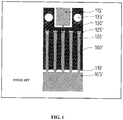
- the source electrodes 100 are connected by air bridges 125 to source pads 130, which are further, connected by a large via 135.
- the drain electrodes 120 are connected to a common drain pad 105; and the gate electrodes 110 are connected to a common gate pad 115.
- the large via is required to make a connection to the back of the substrate (not shown).
- the area required for the nitride semiconductor device is about three times as large as the area of an active region 130 (the area in which source, drain and gate electrodes are located) . It is possible to reduce the size of an electrode pad, but such reduction in size of the electrode pad is limited in view of the yield.
- FIG. 2 illustrates a unique topology, where the adjacent positioning of the substrate contacts (short vias) does not impair the active area density.
- the gate width is greatly increased for a given active area because the gate runs in two dimensions. There are no limitations, except breakdown voltage and line width limits, upon the on-resistance that can be achieved by this topology.
- each source electrode (100) is accompanied by a via (111); each source electrode (100) is surrounded by an adjacent drain electrode (120).
- Each drain electrode (120) is accompanied by a drain bump (105), which is often a conventional ball made of gold.
- the gate electrode is shown as 110, which is connected to a gate strap (175) by a contact (106).
- the gate strap (175) also connects to a gate pad (115). In this manner, each island electrode has its own pad, thereby reducing the size of the overall device.
- the islands, or tiles, shown in Fig. 2 are an embodiment of an overall feature wherein source and drain electrodes must alternate in a two-dimensional topology.
- the source electrode (100) and the drain electrode (120) are preferably formed from titanium and aluminum.
- the gate electrode (110) is preferably formed from palladium.
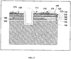
- FIG. 3 illustrates a cross-sectional view taken along I-I' of Fig. 2 .
- a buffer layer (135) is deposited upon the epitaxial layer (140), upon which an undoped gallium nitride layer (130) is deposited.
- a final undoped layer of aluminum 145, and 140 are deposited.
- a buffer layer (135) is deposited upon the epitaxial layer (140), upon which an undoped gallium nitride layer (130) is deposited.
- a final undoped layer of aluminum gallium nitride (125) is deposited upon layer 130.
- the source electrode is shown as 100, which has via (111) thereon, while a drain electrode is shown at 120.
- a gate electrode 110 sits in between the source electrode (100) and the drain electrode (120), upon which is a layer of oxide (170), preferably silicon nitride.
- a gate strap (175) is shown atop the layer 170.
- the rectangular equivalent shown in Fig. 2 may be replaced by any four-sided figure without losing the advantages stated.
- the rectangle can be rotated and an alternative use of the rectangle, for example, is shown in FIG. 5 .
- FIGS. 4 and 5 are extremely advantageous because they allow for increased gate width.
- the source electrodes and vias are shown as 100 and 111 respectively, while the drain electrodes and ball connections are shown as 120 and 105, respectively.
- the gate is run in both directions.
- the active useful gate width is not however doubled since some active area is lost in the transition between individual island devices.
- the island topologies of FIGS. 4 and 5 have been found to provide 1.5 to 1.7 times the gate width. The on-resistance of such devices is proportionately lowered.
- a via (111) is placed on top of a source electrode (100), while a ball connection (105) is atop a drain electrode (120).
- the fuse/antifuse (106) serves to join a gate electrode (110) with a gate strap (175); the gate strap (175) connects to a gate pad (115).
- the gate length is 0.5 microns
- the drain-source spacing is 2.5 microns
- the respective gate widths are: interdigitated, 0.7 meters, rectangular island, 1.1 meters, and triangular island, 1.1 meters.
- a GaN transistor with a 1.4 meter gate width can therefore be made using dice size of less than 3mm x 3mm. Such a device will have an on-resistance of 10-15 milliohms and will be capable of switching 100 Amperes.
- the island topology allows for the spaces between active devices to be used as connection points.
- a low unit resistance metal strap 175 the problem of metal gate resistance can be eliminated.
- the strap can be placed to act as an auxiliary field plate by positioning it separate from the gate as it transits the active gate-drain channel area. This is shown in FIG. 2 and FIG. 3 .
- contact 106 at the gate corners is available. Not forming part of the claimed invention but useful for understanding it, a yield improvement is also possible by isolating individual drains by gold bump removal or absence. Even in the presence of large defect densities it is therefore possible to produce viable functional devices using the layout shown in FIG. 2 .
- FIGS. 2 , 4 , 5 and 6 No provisions for conventional bonds or packages are shown in FIGS. 2 , 4 , 5 and 6 .
- An alternative advantageous packaging technique is shown in a cross-section view in FIG. 7 .
- the absence of air bridges allows the dice (200) to be eutectically bonded (via a eutectic bond (205)) to the copper/source heatsink clip (210).
- This can be inverted to allow the gold bump gate (215) and drain (220) connections to be made directly to copper tracks (225) on a multichip assembly.
- This arrangement greatly reduces the overall area of the mounted device compared to packages that use wire bonds and reduces the inductance of the drain and source connections.
- all of the heat dissipation can be removed through the copper track on board, and the copper/source heatsink clip removed.
- the drain, the source and the gate connections all have gold bumps, no via connections, and an insulative high resistance substrate is used.
- the dice is thinned to 50 microns to achieve lower series resistance to the source connection.
- the package shown in FIG. 7 is used to mechanically strengthen the dice and to ensure that a low inductance connection to the source is obtained.
Description
- The invention relates generally to gallium nitride transistors and, more particularly, to performance improvement and yield enhancement methods associated with the same.
- Gallium nitride materials include gallium nitride and its alloys such as aluminum gallium nitride, indium gallium nitride and aluminum indium gallium nitride. These materials are semiconductor compounds that have a relatively wide, direct bandgap, which permits highly energetic electronic transitions to occur. Gallium nitride materials have a number of attractive properties including high electron mobility, the ability to efficiently emit blue light and the ability to transmit signals at high frequency, among others. Accordingly, gallium nitride materials are being investigated in many microelectronic applications such as transistors and optoelectronic devices.
- Despite the attractive properties noted above, a number of challenges exist in connection with developing gallium nitride material-based devices. For example, it may be difficult to grow high quality gallium nitride materials on certain substrates, particularly silicon, due to property difference (e.g., lattice constant and thermal expansion coefficient) between the gallium nitride material and the substrate material. Also, it has been challenging to form gallium nitride material devices meeting the cost requirements for certain applications.
- High power and medium power gallium nitride microwave transistors are now available and all types use a multifinger structure. Some of the power switching devices described in the research literature also use multifinger structures. Alternative new matrix island based structures are shown herein and these confer significant advantages in all switching applications. Following the practice of all power transistors, the structures are optimized for grounded source circuit applications where it is desirable to minimize the inductance and resistance of the source connection. To this end the transistors are commonly constructed with a series of via connections that subtend the entire vertical structure. These commonly used through-substrate via connections are difficult to manufacture and control. To reach the areas where smaller number of large vias can be made, air bridges may have to be constructed from each of the source connections. See, for example,
US. Pat. No. 7,352,016 B2 . However, air bridges are a source of manufacturing and handling problems. -
U.S. Patent No. 7,550,821 B2 (Shibata et al. ) discloses a nitride semiconductor device in which air bridges are eliminated altogether. A plurality of first electrodes and a plurality of second electrodes are formed (spaced apart from each other) on an active region in a nitride semiconductor layer (which is formed on a main surface of a substrate). An interlayer insulating film is formed on the nitride semiconductor layer. The interlayer insulating film has openings that respectively expose the first electrodes and has a planarized top surface. A first electrode pad is formed in a region over the active region in the interlayer insulating film and is electrically connected to the exposed first electrodes through the respective openings. While the source-substrate contacts (short vias) are placed adjacent to the active areas and are directly connected to the source electrodes, there is an area increase penalty in this multifinger structure. As such, the nitride semiconductor device of Shibata et al. is also accordingly limited by the high on-resistance typical of power switching transistors using conventional multifinger structures. -
US Patent 7,250,641 B2 (Saito et al. ) discloses a nitride semiconductor device that comprises: a silicon substrate; a first aluminum gallium nitride layer formed as a channel layer on the silicon substrate in an island shape; and a second aluminum gallium nitride layer formed as a barrier layer of a first conductive type or i-type on the first aluminum gallium nitride layer. The islands disclosed therein are completely isolated from each other with no common gate electrode between them; each island is thus a separate device. The embodiments disclosed by Saito et al (e.g. as inFig. 1 ) require the juxtaposition of three source electrodes, island to island. The island concept disclosed by Saito et al, serves only as a separation of isolated devices; i.e. there is no intrinsic mode of operation invoked between the islands. - Mesh gate structures are known for power MOSFET devices.
US2004/245638A1 entitled "Semiconductor power device having a diamond shaped metal interconnect scheme", a double diffused metal oxide semiconductor (LDMOS) transistor wherein the polysilicon mesh gate acts as a self-aligned mask for diffusion of dopant to form source and drain regions, and diagonal overlying source metal strips and drain metal strips interconnect individual sources and drains, and another layer of interconnect provides source and drain bump connections.WO9940629A1 US5517046A , entitled "High voltage lateral DMOS device with enhanced drift region", discloses another silicon LDMOS transistor having a polysilicon mesh gate structure, and overlying drain metal strips and source metal strips interconnecting individual sources and drains. -
EP1638147A2 , entitled "III-V nitride semiconductor device and method for fabricating the same", discloses an example of an gallium nitride transistor formed on a conductive substrate, wherein the source electrode is connected through a groove to the conductive substrate to improve the breakdown voltage of the device.EP0069429A2 , entitled "Insulated Gate Field Effect Transistor", discloses a silicon insulated gate field effect transistor wherein, a field plate is provided overlying the gate and connected to the gate to increase the breakdown voltage of the device. - The new topology described herein eliminates source connection air bridges and allows the gate electrode to be tracked in up to two additional directions leading to an on-resistance reduction of 1.5 to 5 times compared with conventional multi-finger structures. In this way the large area requirements of ladder (or multifinger structures) are eliminated.
- A few examples of the present invention may be based upon relatively complex silicon based templates. However this, together with the new island based surface topologies, greatly simplify the costly gallium nitride device process steps.
- The invention in its general form will first be described, and then its implementation in terms of specific designs will be detailed hereafter. These embodiments are intended to demonstrate the principle of the invention, and the manner of its implementation.
- The present invention eliminates the air bridges that are well known to cause power transistor manufacturing and handling difficulties. Both the older gallium arsenide devices and the newer gallium nitride devices suffer yield losses. The present invention provides a topology that in one realization uses a multiplicity of small short vias that make air bridges or through substrate source electrode via connections mechanisms unnecessary. Sources and drains are made to consist only of islands that are reduced in size sufficiently only to allow the positioning of a ball grid or/and via grid within each source and drain. By this unique means bonds are eliminated as well as air bridges.
- The present invention provides nitride semiconductor devices as set out in the independent claims 1 and 2. Advantageous embodiments of the invention are set out in the dependent claims.
- The island electrodes are preferably each a four-sided figure, or preferably triangular shaped. Alternatively, the islands may be a combination of various variants of polygon shapes that allow drain/source juxtapositioning. In addition, the nitride semiconductor device may further comprising one or more epitaxial layers in between the substrate and the nitride semiconductor layer. Each of the epitaxial layer is lightly doped. Field plates may be inserted within the epitaxial layers.
- In the present invention, source island electrodes are always juxtaposed with drain island electrodes, and a gate always exists between them.
- Where it is desirable to use an insulative substrate, the via can be eliminated and replaced by a ball grid identical to that used for the drain islands. The islands, if are each a four-sided figure possessing a two-fold or four-fold symmetry, this allows the gate to run in two directions; if the islands are triangular, then the gate can be run in three directions. As a result the gate track can be much larger for a given dice size. The multifinger structure can be abandoned and sources and drains made to consist only of islands.
- The island topology disclosed herein, preferably triangular or rectangular island structures, provide numerous advantages over the common multi-finger or interdigitated structure. These island topologies result in the specific transistor resistance being less than 70% of those achieved by equivalent-area multi-finger layouts. More significantly, the effective overall device area ratios are 3 to 5 times superior because of the reduced surface interconnect and pad requirements.
- The present invention provides a device with a larger gate width (or "Wg") within a given active area. In certain exemplary embodiments, the topologies provide a great increase in the current handling capability per unit overall device area, rather than just within the active area. In addition, there is provided a simple process to fabricate extremely capable GaN semiconductor devices.
- Another aspect of this invention relates to the design of the field plates buried within various epitaxial layers. Because the silicon conductive substrate will produce unwanted increases in the capacitance of the active regions, a lightly doped singular, dual or a series of epitaxial layers of intrinsic silicon material (lightly doped) can be grown on the substrate. The thickness of this or these layers can be varied and a buried conductive layer or a series of layers can be inserted to act as buried field plates. Multiple field plates of various sizes and shapes can be introduced. These field plates reduce the peak electric field near the gate edge that is juxtaposed to the drain and therefore increases the maximum voltage that the transistor can withstand. In addition, these field plates can be arranged to provide a very even distribution of the electrical stress between the gate edge and the drain edge. A unique and exceptionally linear or very high voltage device can be constructed. The novel vertical epitaxial silicon based structure can in addition assist with problems related to the mechanical stresses that arise due the disparity between the thermal expansion of silicon and gallium nitride.
- The foregoing and other aspects of the present invention will become apparent from the following detailed description of the invention when considered in conjunction with the accompanying drawings.
- Wherever ranges of values are referenced within this specification, sub-ranges therein are intended to be included within the scope of the invention unless otherwise indicated. Where characteristics are attributed to one or another variant of the invention, unless otherwise indicated, such characteristics are intended to apply to all other variants of the invention where such characteristics are appropriate or compatible with such other variants.
- The following is given by way of illustration only and is not to be considered limitative of this invention.
-
-
FIG. 1 illustrates a plan view example of a prior art building block structure. -
FIG. 2 illustrates a plan view of an embodiment of the present invention. -
FIG. 3 illustrates a cross section taken along the line I-I' ofFig. 2 -
FIG. 4 illustrates a plan view of the embodiment shown inFig. 2 . -
FIG. 5 illustrates a plan of a second embodiment of the present invention. -
FIG. 6 illustrates a plan view of a third embodiment of the present invention. -
FIG. 7 illustrates packaging of the embodiment shown inFig. 4 . - In the following detailed description of the invention, reference is made to the accompanying drawings that form a part hereof, and in which is shown, by way of illustration, specific embodiments in which the invention may be practiced. In the drawings, like numerals describe substantially similar components throughout the several views. These embodiments are described in sufficient detail to enable those skilled in the art to practice the invention. Other embodiments may be utilized and structural, logical, and electrical changes may be made. The terms wafer template and substrate used in the following description include any structure having an exposed surface with which to form the circuit structure of the invention. The terms substrate or template are understood to include semiconductor wafers. The terms substrate or template are also used to refer to semiconductor structures during processing, and may include other layers that have been fabricated thereupon. Wafers, templates and substrate include doped and undoped semiconductors, epitaxial semiconductor layers supported by a base semiconductor or insulator, as well as other semiconductor structures well known to one skilled in the art. The term conductor is understood to include semiconductors, and the term insulator is defined to include any material that is less electrically conductive than the materials referred to as conductors. The following detailed description is, therefore, not to be taken in a limiting sense, and the scope of the present invention is defined only by the appended claims.
- The accompanying figures are schematic and are not intended to be drawn to scale. For purpose of clarity, not every component is labeled in every figure.
- The field of the invention pertains generally to high and medium power gallium nitride transistors. More specifically, the invention relates to the transistors that operate at high temperatures where large gallium nitride devices have thermal gradients that impair performance. The connection system for each source and/or drain includes a separate thermal sink. Since all large gallium nitride transistors have a plurality of source/drain electrodes, the schema described allows each source and drain connection to be separately compensated, both resistively and thermally, depending on the particular position of these connections in the overall complex structure of the transistor.
- In cases where the base substrate is heavily doped, the small, short vias are able to provide a low resistance connection to the back of the wafer. The wafer doping level can be chosen to tailor the resistance to the particular needs of every type of transistor. Wafers that are heavily doped enable the formation of positive temperature coefficient resistors that operate reliably over temperature ranges extending to 600°K. Positive temperature coefficient can be chosen to be between 0.11% per °K and 1.1% per °K using wafer doping levels between 10E16cm-3 and 10E18cm-3. The small, short via can be varied in length, depth and/or width to provide appropriate compensation.
- Alternatively where very high temperature (higher than 600°K) and very high performance short term operation is required the resistor temperature coefficients can be chosen so that they reach as low as 10% of their room temperature value. Operation in this alternative mode will counteract the natural tendency of gallium nitride devices to reduce their performance at higher temperatures. Transition temperatures from positive to negative temperature coefficients can be chosen between 600°K and 900°K. While this negative temperature coefficient of resistance is not generally valuable, it is possible to use gold or another suitable dopant to achieve a negative temperature coefficient. The new structure and layout may be used and a suitably employed to provide a series source resistance that has a negative temperature coefficient. It is possible therefore to build a gallium nitride transistor based on the schema proposed herein that exhibits very stable performance over a wide temperature range from below 300 °K to over 600 °K. Extremely simple bias methods and very stable, linear performance may be obtained. However the device design difficulty centers around the problem of balancing the positive effects of the source resistance reduction versus the declining performance of the typical of the intrinsic gallium nitride transistors as the temperature increases.
- In addition to the forgoing novel lateral topology attributes, the vertical arrangements described herein have aspects that notably contribute to the performance of the fabricated transistors. It is known that heavily doped substrates have disadvantages associated with the drain-source and channel-source capacitance. This higher capacitance arises from the fact that the substrate acts as one plate of a capacitor. To obviate the effects of this, a very lightly doped substrate has been used typically. Some of the designs described herein however require a heavily doped bulk substrate. To reduce the capacitance effect another aspect of the vertical structure proposed herein is the novel inclusion of a very lightly doped epitaxial layer or a series of epitaxial layers grown upon the substrate in such a way that an idealized interfacial structure is maintained. Since subsequent process steps involve difficulties related to the massive differences in terms of lattice constant (17%) and expansion coefficient between gallium nitride and silicon, the process steps involving the epitaxial layer or layers is critical. The present invention provides for a strained layer super lattice, which may assist with the further growth of GaN/AlGaN heterolayers. High quality GaN/AlGaN heterolayers can be grown over the epitaxial layer or layers by inserting a GaN AIN super lattice over an AIN buffer layer directly grown on the epitaxial layer or layers. The epitaxial layer or layers can be grown to extend, for example, over a thickness range of 3 to 20 microns. When microwave transistors are fabricated the smaller capacitance is preferred since it can be chosen to be part of the required matching network. However this will require the capacitance to be a minimum and the required epitaxial layer thickness will be at a maximum. The 20-micron dimension may be extended to further reduce the capacitance.
- It is known that it is important to reduce the electric field stress at gate edge. It has become common practice to extend the drain side of the gate edge over the SiN or other surface passivation. In some realizations, devices with a drain-gate spacing of 2.5 micron have a surface field plate extended 1.0 micron from the gate toward the drain. This extension results in an unwanted increase in gate-drain feedback capacitance. This noticeably reduces the gain of the device. Alternative schemes involve a metal field plate connected to the source and placed over the gate. The new proposed structures described herein employ a source connected buried layer that extends below the gate to the gate edge (or beyond) facing the drain. Further gains in field stress reduction arise from the conductive substrate below the epitaxial layer. Each or any of the epitaxial layers, where several are used, may contain a buried layer acting as a field plate below the gate. The combination of a buried field plate or plates and the conductive substrate obviates the absolute need for metal surface mounted field plates. The combination of surface field plates and the proposed buried field plates will provide very high breakdown voltage performance. It is possible, where the epitaxial layer is thin that a buried layer field plate is not required resulting in a simplified process. A choice can be made between reducing drain-source capacitance or alternatively reducing the field stress, resulting in an ideal epitaxial thickness of each transistor application.
- The reduced peak electric field for the transistor device of the present invention compared to a simple transistor device results from reduced field crowding at the drain side edge of the gate electrode. This reduction is attributed to the singular or combinational effects of the novel field plates that act to provide the same stress reduction or additional stress reduction that surface field plates provide. The stress reduction leads to improved electrical performance characteristics including increased operation voltage and/or reduced gate leakage current.
- Gallium nitride has a different crystal structure than silicon and when gallium nitride structure is formed on silicon substrates, dislocations may result. Defects and dislocations that are in the vicinity of an active region can greatly impair device performance. Because of the novel layout style of the proposed devices, it is possible to electrically isolate defective individual transistors and remove them from the main structure by disconnecting the gate connection of the defective device. Alternatively or additionally, in an embodiment not forming part of the present invention, the drain connection of the defective device can be disconnected. In the particular case of a normally-off transistor it may be sufficient to just disconnect the gate electrode. The disconnection mechanism could be based on a fuse or laser methodology. Owing to the leakage current or capacitive coupling involved, it may be additionally necessary to ground the gate electrode to the source electrode. A metal-to-metal short circuit can be achieved with a high-energy laser.
- In the conventional design used in prior art (
FIG. 1 ), thesource electrodes 100 are connected byair bridges 125 to sourcepads 130, which are further, connected by a large via 135. As shown thedrain electrodes 120 are connected to acommon drain pad 105; and thegate electrodes 110 are connected to acommon gate pad 115. In these illustrative unit cells, ten gate electrodes are connected to the gate pad and five drain electrodes are connected to the drain pad. In addition the large via is required to make a connection to the back of the substrate (not shown). In this case, the area required for the nitride semiconductor device is about three times as large as the area of an active region 130 (the area in which source, drain and gate electrodes are located) . It is possible to reduce the size of an electrode pad, but such reduction in size of the electrode pad is limited in view of the yield. -
FIG. 2 illustrates a unique topology, where the adjacent positioning of the substrate contacts (short vias) does not impair the active area density. In this topology, the gate width is greatly increased for a given active area because the gate runs in two dimensions. There are no limitations, except breakdown voltage and line width limits, upon the on-resistance that can be achieved by this topology. Here, each source electrode (100) is accompanied by a via (111); each source electrode (100) is surrounded by an adjacent drain electrode (120). Each drain electrode (120) is accompanied by a drain bump (105), which is often a conventional ball made of gold. The gate electrode is shown as 110, which is connected to a gate strap (175) by a contact (106). The gate strap (175) also connects to a gate pad (115). In this manner, each island electrode has its own pad, thereby reducing the size of the overall device. The islands, or tiles, shown inFig. 2 , are an embodiment of an overall feature wherein source and drain electrodes must alternate in a two-dimensional topology. The source electrode (100) and the drain electrode (120) are preferably formed from titanium and aluminum. The gate electrode (110) is preferably formed from palladium. -
FIG. 3 illustrates a cross-sectional view taken along I-I' ofFig. 2 . A substrate (155), preferably made of silicon, forms a base upon which successive insulatingepitaxial layers aluminum layer 130. Within the threeepitaxial layers field plates gate electrode 110 sits in between the source electrode (100) and the drain electrode (120), upon which is a layer of oxide (170), preferably silicon nitride. A gate strap (175) is shown atop thelayer 170. - The rectangular equivalent shown in
Fig. 2 may be replaced by any four-sided figure without losing the advantages stated. The rectangle can be rotated and an alternative use of the rectangle, for example, is shown inFIG. 5 . - These two-dimensional tiled layouts shown in
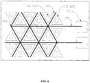
FIGS. 4 and5 are extremely advantageous because they allow for increased gate width. In bothFigures 4 and5 , the source electrodes and vias are shown as 100 and 111 respectively, while the drain electrodes and ball connections are shown as 120 and 105, respectively. The gate is run in both directions. The active useful gate width is not however doubled since some active area is lost in the transition between individual island devices. In practice, compared with multifinger device layouts, the island topologies ofFIGS. 4 and5 have been found to provide 1.5 to 1.7 times the gate width. The on-resistance of such devices is proportionately lowered. - It is possible to also enhance the gate width by running the gate in three directions. This is shown in the island layout of
FIG. 6 where a unique equilateral triangle island is used. The triangle can however be of any format and the concept of running the gate in three directions is not limited to the convenient equilateral triangle layout shown. In practice this layout also provides approximately 1.5 to 1.7 times the gate width obtained by using interdigitated (or multifingered) structures of the prior art. As inFig. 2 , a via (111) is placed on top of a source electrode (100), while a ball connection (105) is atop a drain electrode (120). The fuse/antifuse (106) serves to join a gate electrode (110) with a gate strap (175); the gate strap (175) connects to a gate pad (115). - Based on design rules where the gate length is 0.5 microns, the drain-source spacing is 2.5 microns, there are 7.5 micron drain/source features and where the active area is 7.5mm2, the respective gate widths are: interdigitated, 0.7 meters, rectangular island, 1.1 meters, and triangular island, 1.1 meters. A GaN transistor with a 1.4 meter gate width can therefore be made using dice size of less than 3mm x 3mm. Such a device will have an on-resistance of 10-15 milliohms and will be capable of switching 100 Amperes.
- The island topology allows for the spaces between active devices to be used as connection points. By using a low unit
resistance metal strap 175 the problem of metal gate resistance can be eliminated. The strap can be placed to act as an auxiliary field plate by positioning it separate from the gate as it transits the active gate-drain channel area. This is shown inFIG. 2 andFIG. 3 . - To use the strap only to connect to good functional individual cells, contact 106 at the gate corners is available. Not forming part of the claimed invention but useful for understanding it, a yield improvement is also possible by isolating individual drains by gold bump removal or absence. Even in the presence of large defect densities it is therefore possible to produce viable functional devices using the layout shown in
FIG. 2 . - No provisions for conventional bonds or packages are shown in
FIGS. 2 ,4 ,5 and6 . An alternative advantageous packaging technique is shown in a cross-section view inFIG. 7 . The absence of air bridges allows the dice (200) to be eutectically bonded (via a eutectic bond (205)) to the copper/source heatsink clip (210). This can be inverted to allow the gold bump gate (215) and drain (220) connections to be made directly to copper tracks (225) on a multichip assembly. This arrangement greatly reduces the overall area of the mounted device compared to packages that use wire bonds and reduces the inductance of the drain and source connections. - Alternatively, all of the heat dissipation can be removed through the copper track on board, and the copper/source heatsink clip removed. To achieve this result, the drain, the source and the gate connections all have gold bumps, no via connections, and an insulative high resistance substrate is used.
- It is common practice to thin the wafers of power R.F. devices from about 450 microns to 150 microns to lower the thermal resistance. In a packaged device, shown in
FIG. 7 , the dice is thinned to 50 microns to achieve lower series resistance to the source connection. The package shown inFIG. 7 is used to mechanically strengthen the dice and to ensure that a low inductance connection to the source is obtained. - The foregoing has constituted a description of specific embodiments showing how the invention may be applied and put into use. These embodiments are only exemplary. The invention in its broadest, and more specific aspects is further described and defined in the claims which now follow.
Claims (11)
- A nitride semiconductor device comprising:a) a substrate (155);b) a nitride semiconductor layer formed on a main surface of the substrate;c) a plurality of source island electrodes (100) and a plurality of drain island electrodes (120) of a multi-island field effect transistor, the source island electrodes and drain island electrodes being formed on the nitride semiconductor layer, spaced apart from each other and alternately arranged in a matrix arrangement to produce active regions therebetween in a device area of the nitride semiconductor layer, wherein, for each pair of adjacent source and drain island electrodes, a respective side of the source island electrode is juxtaposed with a respective side of the drain island electrode;d) a plurality of gate electrodes (110) formed on said active regions, wherein a respective gate electrode is formed between each pair of adjacent source and drain island electrodes, a low resistance gate interconnect (175) consisting of low resistance metal straps, the plurality of gate electrodes being interconnected to the low resistance gate interconnect by interconnections (106) at interstices defined by adjacent vertices of the source island electrodes and drain island electrodes;e) each of the plurality of source island electrodes (100) having a respective individual bump or ball connection (105) formed thereon;f) each of the plurality of drain island electrodes (120) having a respective individual bump or ball connection (105) formed thereon;
andg) the low resistance gate interconnect (175) being connected to a plurality of gate pads (115). - A nitride semiconductor device comprising:a) a conductive substrate (155);b) a nitride semiconductor layer formed on a main surface of the substrate;c) a plurality of source island electrodes (100) and a plurality of drain island electrodes (120) of a multi-island field effect transistor, the source island electrodes and drain island electrodes being formed on the nitride semiconductor layer, spaced apart from each other and alternately arranged in a matrix arrangement to produce active regions therebetween in a device area of the nitride semiconductor layer, wherein, for each pair of adjacent source and drain island electrodes, a respective side of the source island electrode is juxtaposed with a respective side of the drain island electrode;d) a plurality of gate electrodes (110) formed on said active regions, wherein a respective gate electrode is formed between each pair of adjacent source and drain island electrodes, a low resistance gate interconnect (175) consisting of low resistance metal straps, the plurality of gate electrodes being interconnected to the low resistance gate interconnect by interconnections (106) at interstices defined by adjacent vertices of the source island electrodes and the drain island electrodes;e) each of the plurality of source island electrodes (100) having a respective individual via connection (111) to the conductive substrate;f) each of the plurality of drain island electrodes (120) having a respective individual bump or ball connection (105) formed thereon;
andg) the low resistance gate interconnect (175) being connected to a plurality of gate pads (115). - The device of claim 1 or 2, wherein the drain and source island electrodes are each a four-sided figure.
- The device of claim 1 or 2, wherein the drain and source island electrodes are triangular shaped.
- The device of claim 1 or 2, wherein each of the drain and source island electrodes have a polygon shape that allows drain/source juxtapositioning.
- The device of any one of claims 1 to 5, further comprising one or more epitaxial layers in between said substrate and said nitride semiconductor layer.
- The device of claim 6, wherein said one or more epitaxial layers are lightly doped.
- The device of claim 6 or 7, comprising a plurality of said epitaxial layers and further comprising one or more field plates, wherein each said field plate is positioned between successive epitaxial layers.
- The device of any one of claims 1 to 8, wherein said bump or ball connections are formed of gold.
- The device of any one of claims 1 to 9, wherein the nitride semiconductor layer comprises a hetero-layer consisting of a layer of undoped gallium nitride beneath a layer of undoped aluminum gallium nitride.
- The device of claim 1, wherein each of the gate electrodes is formed from palladium, and each of the source and drain island electrodes are made from titanium and aluminum.
Applications Claiming Priority (2)
| Application Number | Priority Date | Filing Date | Title |
|---|---|---|---|
| US23113909P | 2009-08-04 | 2009-08-04 | |
| PCT/CA2010/001202 WO2011014951A1 (en) | 2009-08-04 | 2010-08-04 | Island matrixed gallium nitride microwave and power switching transistors |
Publications (3)
| Publication Number | Publication Date |
|---|---|
| EP2465141A1 EP2465141A1 (en) | 2012-06-20 |
| EP2465141A4 EP2465141A4 (en) | 2017-04-26 |
| EP2465141B1 true EP2465141B1 (en) | 2021-04-07 |
Family
ID=43543843
Family Applications (1)
| Application Number | Title | Priority Date | Filing Date |
|---|---|---|---|
| EP10805910.6A Active EP2465141B1 (en) | 2009-08-04 | 2010-08-04 | Gallium nitride microwave and power switching transistors with matrix layout |
Country Status (7)
| Country | Link |
|---|---|
| US (1) | US9064947B2 (en) |
| EP (1) | EP2465141B1 (en) |
| JP (1) | JP5985393B2 (en) |
| KR (1) | KR20120041237A (en) |
| AU (1) | AU2010281317A1 (en) |
| CA (1) | CA2769940C (en) |
| WO (1) | WO2011014951A1 (en) |
Families Citing this family (22)
| Publication number | Priority date | Publication date | Assignee | Title |
|---|---|---|---|---|
| US9029866B2 (en) | 2009-08-04 | 2015-05-12 | Gan Systems Inc. | Gallium nitride power devices using island topography |
| WO2011014951A1 (en) | 2009-08-04 | 2011-02-10 | John Roberts | Island matrixed gallium nitride microwave and power switching transistors |
| US9818857B2 (en) | 2009-08-04 | 2017-11-14 | Gan Systems Inc. | Fault tolerant design for large area nitride semiconductor devices |
| DE102010001788A1 (en) * | 2010-02-10 | 2011-08-11 | Forschungsverbund Berlin e.V., 12489 | Scalable structure for lateral semiconductor devices with high current carrying capacity |
| KR20130088743A (en) | 2010-04-13 | 2013-08-08 | 갠 시스템즈 인크. | High density gallium nitride devices using island topology |
| US9159743B2 (en) * | 2011-11-09 | 2015-10-13 | Skyworks Solutions, Inc. | Radio-frequency switches having silicon-on-insulator field-effect transistors with reduced linear region resistance |
| FR2984429B1 (en) | 2011-12-16 | 2014-02-14 | Snecma | VIBRATION DAMPING BANDS WITH FLUID EXHAUST, FOR ACOUSTIC PROTECTION OF AIRCRAFT TURBOMACHINE BLOWER HOUSING |
| US20140027778A1 (en) * | 2012-07-25 | 2014-01-30 | International Rectifier Corporation | Robust Fused Transistor |
| US9331154B2 (en) * | 2013-08-21 | 2016-05-03 | Epistar Corporation | High electron mobility transistor |
| KR101837877B1 (en) * | 2013-10-29 | 2018-03-12 | 갠 시스템즈 인크. | Fault tolerant design for large area nitride semiconductor devices |
| KR101729653B1 (en) | 2013-12-30 | 2017-04-25 | 한국전자통신연구원 | Nitride semiconductor device |
| GB201418752D0 (en) * | 2014-10-22 | 2014-12-03 | Rolls Royce Plc | Lateral field effect transistor device |
| DE102016103581B4 (en) | 2016-02-29 | 2019-11-14 | Infineon Technologies Austria Ag | A semiconductor device with needle-shaped field plates and a gate structure with edge and node regions |
| US9842920B1 (en) | 2016-07-12 | 2017-12-12 | Semiconductor Components Industries, Llc | Gallium nitride semiconductor device with isolated fingers |
| US10147796B1 (en) * | 2017-05-26 | 2018-12-04 | Stmicroelectronics Design And Application S.R.O. | Transistors with dissimilar square waffle gate patterns |
| US10403624B2 (en) | 2017-05-26 | 2019-09-03 | Stmicroelectronics Design And Application S.R.O. | Transistors with octagon waffle gate patterns |
| US10529802B2 (en) | 2017-09-14 | 2020-01-07 | Gan Systems Inc. | Scalable circuit-under-pad device topologies for lateral GaN power transistors |
| US10218346B1 (en) | 2017-09-14 | 2019-02-26 | Gan Systems Inc. | High current lateral GaN transistors with scalable topology and gate drive phase equalization |
| US11082039B2 (en) | 2017-11-08 | 2021-08-03 | Gan Systems Inc. | GaN transistor with integrated drain voltage sense for fast overcurrent and short circuit protection |
| US11387169B2 (en) | 2020-08-04 | 2022-07-12 | Nxp Usa, Inc. | Transistor with I/O ports in an active area of the transistor |
| US11502026B2 (en) | 2020-10-12 | 2022-11-15 | Nxp Usa, Inc. | Transistor with flip-chip topology and power amplifier containing same |
| US11587852B2 (en) | 2020-10-12 | 2023-02-21 | Nxp Usa, Inc. | Power amplifier modules with flip-chip and non-flip-chip power transistor dies |
Citations (2)
| Publication number | Priority date | Publication date | Assignee | Title |
|---|---|---|---|---|
| US6084266A (en) * | 1998-03-02 | 2000-07-04 | Vanguard International Semiconductor Corporation | Layout of semiconductor devices to increase the packing density of a wafer |
| US20060131745A1 (en) * | 2004-12-14 | 2006-06-22 | Mitsubishi Denki Kabushiki Kaisha | Semiconductor device and manufacturing method therefor |
Family Cites Families (125)
| Publication number | Priority date | Publication date | Assignee | Title |
|---|---|---|---|---|
| US3783349A (en) | 1971-05-25 | 1974-01-01 | Harris Intertype Corp | Field effect transistor |
| JPS5631752B2 (en) * | 1973-08-31 | 1981-07-23 | ||
| JPS5089263U (en) * | 1973-12-14 | 1975-07-29 | ||
| JPS5181067U (en) * | 1974-12-20 | 1976-06-28 | ||
| US4152714A (en) * | 1978-01-16 | 1979-05-01 | Honeywell Inc. | Semiconductor apparatus |
| NL8103218A (en) * | 1981-07-06 | 1983-02-01 | Philips Nv | FIELD-EFFECT TRANSISTOR WITH INSULATED HANDLEBAR ELECTRODE. |
| JPS5868954A (en) * | 1981-10-20 | 1983-04-25 | Mitsubishi Electric Corp | Package for high frequency transistor |
| US4819042A (en) * | 1983-10-31 | 1989-04-04 | Kaufman Lance R | Isolated package for multiple semiconductor power components |
| US4636825A (en) | 1985-10-04 | 1987-01-13 | Fairchild Semiconductor Corporation | Distributed field effect transistor structure |
| JPH07112064B2 (en) | 1986-02-10 | 1995-11-29 | 株式会社東芝 | Insulated gate field effect transistor |
| US5068603A (en) * | 1987-10-07 | 1991-11-26 | Xilinx, Inc. | Structure and method for producing mask-programmed integrated circuits which are pin compatible substitutes for memory-configured logic arrays |
| JP2679333B2 (en) * | 1990-02-26 | 1997-11-19 | 日本電気株式会社 | Schottky barrier junction gate type field effect transistor |
| JP3039021B2 (en) | 1991-08-13 | 2000-05-08 | 松下電器産業株式会社 | Manufacturing method of rotary transformer |
| JPH0589263A (en) | 1991-09-30 | 1993-04-09 | Sanyo Electric Co Ltd | Data processor |
| JP2948007B2 (en) | 1991-12-26 | 1999-09-13 | 日立電子株式会社 | Fine movement stage |
| US5355008A (en) | 1993-11-19 | 1994-10-11 | Micrel, Inc. | Diamond shaped gate mesh for cellular MOS transistor array |
| US5517046A (en) | 1993-11-19 | 1996-05-14 | Micrel, Incorporated | High voltage lateral DMOS device with enhanced drift region |
| KR0137975B1 (en) | 1994-01-19 | 1998-06-15 | 김주용 | Semiconductor device & process for manufacturing the same |
| JP3113153B2 (en) * | 1994-07-26 | 2000-11-27 | 株式会社東芝 | Semiconductor device with multilayer wiring structure |
| US5767546A (en) | 1994-12-30 | 1998-06-16 | Siliconix Incorporated | Laternal power mosfet having metal strap layer to reduce distributed resistance |
| DE19581809B4 (en) | 1995-04-06 | 2008-12-24 | Transpacific Ip, Ltd. | MOS cell, multiple cell transistor and IC chip |
| US5714784A (en) | 1995-10-19 | 1998-02-03 | Winbond Electronics Corporation | Electrostatic discharge protection device |
| US6353290B1 (en) * | 1996-03-06 | 2002-03-05 | The United States Of America As Represented By The Secretary Of The Army | Microwave field emitter array limiter |
| US5789791A (en) | 1996-08-27 | 1998-08-04 | National Semiconductor Corporation | Multi-finger MOS transistor with reduced gate resistance |
| US6639277B2 (en) | 1996-11-05 | 2003-10-28 | Power Integrations, Inc. | High-voltage transistor with multi-layer conduction region |
| JP3499103B2 (en) | 1997-02-21 | 2004-02-23 | 三菱電機株式会社 | Semiconductor device |
| US6002156A (en) | 1997-09-16 | 1999-12-14 | Winbond Electronics Corp. | Distributed MOSFET structure with enclosed gate for improved transistor size/layout area ratio and uniform ESD triggering |
| US6037822A (en) * | 1997-09-30 | 2000-03-14 | Intel Corporation | Method and apparatus for distributing a clock on the silicon backside of an integrated circuit |
| US7560296B2 (en) * | 2000-07-07 | 2009-07-14 | Lumilog | Process for producing an epitalixal layer of galium nitride |
| JP3441353B2 (en) * | 1998-01-29 | 2003-09-02 | 京セラ株式会社 | Field-effect transistor |
| CN1290403A (en) * | 1998-02-07 | 2001-04-04 | 斋摩德股份有限公司 | Quasi-mesh gate structure including plugs connecting source regious with backside for lateral RF MOS devices |
| US6100549A (en) * | 1998-08-12 | 2000-08-08 | Motorola, Inc. | High breakdown voltage resurf HFET |
| JP2000208759A (en) * | 1999-01-12 | 2000-07-28 | Rohm Co Ltd | Semiconductor device |
| JP3587081B2 (en) | 1999-05-10 | 2004-11-10 | 豊田合成株式会社 | Method of manufacturing group III nitride semiconductor and group III nitride semiconductor light emitting device |
| JP2001028425A (en) * | 1999-07-15 | 2001-01-30 | Mitsubishi Electric Corp | Semiconductor device and manufacture thereof |
| US6580098B1 (en) | 1999-07-27 | 2003-06-17 | Toyoda Gosei Co., Ltd. | Method for manufacturing gallium nitride compound semiconductor |
| GB9919479D0 (en) | 1999-08-17 | 1999-10-20 | Imperial College | Island arrays |
| JP4362905B2 (en) | 1999-09-21 | 2009-11-11 | 富士ゼロックス株式会社 | Self-scanning light-emitting device, light source for writing, and optical printer |
| EP1258040A4 (en) * | 2000-02-10 | 2009-07-01 | Int Rectifier Corp | Vertical conduction flip-chip device with bump contacts on single surface |
| JP4629826B2 (en) | 2000-02-22 | 2011-02-09 | パナソニック株式会社 | Semiconductor integrated circuit device |
| TW518767B (en) | 2000-03-31 | 2003-01-21 | Toyoda Gosei Kk | Production method of III nitride compound semiconductor and III nitride compound semiconductor element |
| WO2001080311A1 (en) | 2000-04-17 | 2001-10-25 | Virginia Commonwealth University | Defect reduction in gan and related materials |
| US6627974B2 (en) | 2000-06-19 | 2003-09-30 | Nichia Corporation | Nitride semiconductor substrate and method for manufacturing the same, and nitride semiconductor device using nitride semiconductor substrate |
| US6477023B1 (en) | 2000-07-12 | 2002-11-05 | United Microelectronics Corp. | Electrostatic discharge protection apparatus |
| AU2001273458A1 (en) | 2000-07-13 | 2002-01-30 | Isothermal Systems Research, Inc. | Power semiconductor switching devices, power converters, integrated circuit assemblies, integrated circuitry, power current switching methods, methods of forming a power semiconductor switching device, power conversion methods, power semiconductor switching device packaging methods, and methods of forming a power transistor |
| US6690042B2 (en) * | 2000-09-27 | 2004-02-10 | Sensor Electronic Technology, Inc. | Metal oxide semiconductor heterostructure field effect transistor |
| US6548333B2 (en) | 2000-12-01 | 2003-04-15 | Cree, Inc. | Aluminum gallium nitride/gallium nitride high electron mobility transistors having a gate contact on a gallium nitride based cap segment |
| US7233028B2 (en) | 2001-02-23 | 2007-06-19 | Nitronex Corporation | Gallium nitride material devices and methods of forming the same |
| JP3763753B2 (en) | 2001-06-05 | 2006-04-05 | 豊田合成株式会社 | Group III nitride compound semiconductor device and method for manufacturing the same |
| KR20040029301A (en) | 2001-08-22 | 2004-04-06 | 소니 가부시끼 가이샤 | Nitride semiconductor element and production method for nitride semiconductor element |
| US7398498B2 (en) * | 2001-08-23 | 2008-07-08 | Cadence Design Systems, Inc. | Method and apparatus for storing routes for groups of related net configurations |
| US6555873B2 (en) | 2001-09-07 | 2003-04-29 | Power Integrations, Inc. | High-voltage lateral transistor with a multi-layered extended drain structure |
| US6894397B2 (en) * | 2001-10-03 | 2005-05-17 | International Rectifier Corporation | Plural semiconductor devices in monolithic flip chip |
| JP3524908B2 (en) | 2002-01-21 | 2004-05-10 | 株式会社半導体理工学研究センター | Semiconductor device |
| US6713823B1 (en) * | 2002-03-08 | 2004-03-30 | Volterra Semiconductor Corporation | Conductive routings in integrated circuits |
| JP3968566B2 (en) | 2002-03-26 | 2007-08-29 | 日立電線株式会社 | Nitride semiconductor crystal manufacturing method, nitride semiconductor wafer, and nitride semiconductor device |
| US6724044B2 (en) * | 2002-05-10 | 2004-04-20 | General Semiconductor, Inc. | MOSFET device having geometry that permits frequent body contact |
| US20030218246A1 (en) * | 2002-05-22 | 2003-11-27 | Hirofumi Abe | Semiconductor device passing large electric current |
| US7253486B2 (en) | 2002-07-31 | 2007-08-07 | Freescale Semiconductor, Inc. | Field plate transistor with reduced field plate resistance |
| AU2003270578A1 (en) * | 2002-09-10 | 2004-04-30 | The Regents Of The University Of California | Interconnection architecture and method of assessing interconnection architecture |
| TW560120B (en) | 2002-09-20 | 2003-11-01 | Chung Shan Inst Of Science | Nitride based semiconductor laser diode device including a selective growth mask |
| US6972464B2 (en) | 2002-10-08 | 2005-12-06 | Great Wall Semiconductor Corporation | Power MOSFET |
| JP4232584B2 (en) | 2002-10-15 | 2009-03-04 | 株式会社デンソー | Semiconductor device |
| JP4396200B2 (en) | 2002-10-30 | 2010-01-13 | 株式会社デンソー | Semiconductor device |
| JP4510370B2 (en) | 2002-12-25 | 2010-07-21 | パナソニック株式会社 | Semiconductor integrated circuit device |
| KR100493059B1 (en) * | 2003-04-18 | 2005-06-02 | 삼성전자주식회사 | Transistor decreasing gate capacitance |
| US6897561B2 (en) | 2003-06-06 | 2005-05-24 | Semiconductor Components Industries, Llc | Semiconductor power device having a diamond shaped metal interconnect scheme |
| US7135720B2 (en) | 2003-08-05 | 2006-11-14 | Nitronex Corporation | Gallium nitride material transistors and methods associated with the same |
| JP2005117020A (en) | 2003-09-16 | 2005-04-28 | Stanley Electric Co Ltd | Gallium nitride based compound semiconductor device and its manufacturing method |
| KR100799857B1 (en) | 2003-10-27 | 2008-01-31 | 삼성전기주식회사 | Electrode structure and semiconductor light-emitting device provided with the same |
| DE102004058431B4 (en) * | 2003-12-05 | 2021-02-18 | Infineon Technologies Americas Corp. | III-nitride semiconductor device with trench structure |
| JP4667756B2 (en) * | 2004-03-03 | 2011-04-13 | 三菱電機株式会社 | Semiconductor device |
| US7622318B2 (en) | 2004-03-30 | 2009-11-24 | Sony Corporation | Method for producing structured substrate, structured substrate, method for producing semiconductor light emitting device, semiconductor light emitting device, method for producing semiconductor device, semiconductor device, method for producing device, and device |
| JP4810072B2 (en) | 2004-06-15 | 2011-11-09 | 株式会社東芝 | Nitrogen compound-containing semiconductor devices |
| US7943949B2 (en) | 2004-09-09 | 2011-05-17 | Bridgelux, Inc. | III-nitride based on semiconductor device with low-resistance ohmic contacts |
| JP2006086398A (en) * | 2004-09-17 | 2006-03-30 | Matsushita Electric Ind Co Ltd | Semiconductor device and its manufacturing method |
| US20060073621A1 (en) | 2004-10-01 | 2006-04-06 | Palo Alto Research Center Incorporated | Group III-nitride based HEMT device with insulating GaN/AlGaN buffer layer |
| JP4272142B2 (en) | 2004-12-07 | 2009-06-03 | 株式会社ルネサステクノロジ | Switching element, antenna switch circuit and high-frequency module using the same |
| US7906788B2 (en) | 2004-12-22 | 2011-03-15 | Panasonic Corporation | Semiconductor light emitting device, illumination module, illumination apparatus, method for manufacturing semiconductor light emitting device, and method for manufacturing semiconductor light emitting element |
| TWI261891B (en) * | 2004-12-24 | 2006-09-11 | Richtek Technology Corp | Power metal oxide semiconductor transistor layout with lower output resistance and high current limit |
| JP5076278B2 (en) * | 2005-03-14 | 2012-11-21 | 日亜化学工業株式会社 | Field effect transistor |
| US7294892B2 (en) | 2005-05-27 | 2007-11-13 | Faraday Technology Corp. | Multi-transistor layout capable of saving area |
| JP4705412B2 (en) * | 2005-06-06 | 2011-06-22 | パナソニック株式会社 | Field effect transistor and manufacturing method thereof |
| JP2007103451A (en) | 2005-09-30 | 2007-04-19 | Toshiba Corp | Semiconductor device and its manufacturing method |
| JP5140962B2 (en) * | 2005-10-28 | 2013-02-13 | 日亜化学工業株式会社 | Manufacturing method of nitride semiconductor substrate |
| EP1801855B1 (en) | 2005-12-22 | 2009-01-14 | Freiberger Compound Materials GmbH | Processes for selective masking of III-N layers and for the preparation of free-standing III-N layers or of devices |
| JP2007305954A (en) * | 2006-03-27 | 2007-11-22 | Nichia Chem Ind Ltd | Field-effect transistor and its device |
| US7449762B1 (en) * | 2006-04-07 | 2008-11-11 | Wide Bandgap Llc | Lateral epitaxial GaN metal insulator semiconductor field effect transistor |
| KR100782430B1 (en) | 2006-09-22 | 2007-12-05 | 한국과학기술원 | Gan-hemt (high electron mobility transistor) structure with inner field-plate structure for high power applications |
| JP5047575B2 (en) | 2006-09-29 | 2012-10-10 | 三井化学株式会社 | Surface protection film |
| US7964895B2 (en) * | 2006-10-05 | 2011-06-21 | International Rectifier Corporation | III-nitride heterojunction semiconductor device and method of fabrication |
| JP5186096B2 (en) | 2006-10-12 | 2013-04-17 | パナソニック株式会社 | Nitride semiconductor transistor and manufacturing method thereof |
| JP5105160B2 (en) | 2006-11-13 | 2012-12-19 | クリー インコーポレイテッド | Transistor |
| JP5300238B2 (en) * | 2006-12-19 | 2013-09-25 | パナソニック株式会社 | Nitride semiconductor device |
| JP5082752B2 (en) | 2006-12-21 | 2012-11-28 | 日亜化学工業株式会社 | Manufacturing method of substrate for semiconductor light emitting device and semiconductor light emitting device using the same |
| GB2447509A (en) * | 2007-03-16 | 2008-09-17 | Seiko Epson Corp | Pattern for Inkjet TFT circuit development |
| US8212290B2 (en) * | 2007-03-23 | 2012-07-03 | Cree, Inc. | High temperature performance capable gallium nitride transistor |
| US7675131B2 (en) * | 2007-04-05 | 2010-03-09 | Micron Technology, Inc. | Flip-chip image sensor packages and methods of fabricating the same |
| WO2008141324A2 (en) * | 2007-05-14 | 2008-11-20 | S.O.I.Tec Silicon On Insulator Technologies | Methods for improving the quality of epitaxially-grown semiconductor materials |
| JP4956281B2 (en) | 2007-05-29 | 2012-06-20 | キヤノン株式会社 | Wireless communication apparatus and control method thereof |
| JP2008311355A (en) | 2007-06-13 | 2008-12-25 | Rohm Co Ltd | Nitride semiconductor element |
| JP5089263B2 (en) | 2007-06-20 | 2012-12-05 | 中国電力株式会社 | Air mixing suppression device |
| KR101355593B1 (en) | 2007-07-26 | 2014-01-24 | 아리조나 보드 오브 리젠츠 퍼 앤 온 비하프 오브 아리조나 스테이트 유니버시티 | Methods for producing improved epitaxial materials |
| JP5307991B2 (en) * | 2007-07-27 | 2013-10-02 | セミコンダクター・コンポーネンツ・インダストリーズ・リミテッド・ライアビリティ・カンパニー | Semiconductor device |
| GB2451884A (en) | 2007-08-16 | 2009-02-18 | Sharp Kk | A Semiconductor Device and a Method of Manufacture Thereof |
| JP2009076866A (en) * | 2007-08-31 | 2009-04-09 | Sumitomo Electric Ind Ltd | Schottky barrier diode |
| JP4762217B2 (en) | 2007-09-28 | 2011-08-31 | 富士フイルム株式会社 | Light guide plate, light guide plate unit, and planar illumination device |
| US20110041890A1 (en) * | 2007-11-19 | 2011-02-24 | Sheats James R | High-efficiency, high current solar cell and solar module |
| US8085553B1 (en) * | 2007-12-27 | 2011-12-27 | Volterra Semiconductor Corporation | Lead assembly for a flip-chip power switch |
| US7989953B1 (en) * | 2007-12-28 | 2011-08-02 | Volterra Semiconductor Corporation | Flip chip power switch with under bump metallization stack |
| US20090242961A1 (en) * | 2008-03-31 | 2009-10-01 | Sanh Tang | Recessed channel select gate for a memory device |
| US8343824B2 (en) * | 2008-04-29 | 2013-01-01 | International Rectifier Corporation | Gallium nitride material processing and related device structures |
| CN101299439B (en) * | 2008-06-24 | 2011-06-22 | 广州南科集成电子有限公司 | High pressure resistant constant-current source device and production method |
| WO2010013195A1 (en) * | 2008-07-28 | 2010-02-04 | Nxp B.V. | Integrated circuit and method for manufacturing an integrated circuit |
| EP2151852B1 (en) | 2008-08-06 | 2020-01-15 | Soitec | Relaxation and transfer of strained layers |
| US8367520B2 (en) | 2008-09-22 | 2013-02-05 | Soitec | Methods and structures for altering strain in III-nitride materials |
| US9117944B2 (en) | 2008-09-24 | 2015-08-25 | Koninklijke Philips N.V. | Semiconductor light emitting devices grown on composite substrates |
| JP5533661B2 (en) | 2008-10-29 | 2014-06-25 | 富士通株式会社 | Compound semiconductor device and manufacturing method thereof |
| US7851856B2 (en) * | 2008-12-29 | 2010-12-14 | Alpha & Omega Semiconductor, Ltd | True CSP power MOSFET based on bottom-source LDMOS |
| JP5487631B2 (en) | 2009-02-04 | 2014-05-07 | 富士通株式会社 | Compound semiconductor device and manufacturing method thereof |
| CN102388441B (en) | 2009-04-08 | 2014-05-07 | 宜普电源转换公司 | Enhancement mode GaN HEMT device and method for fabricating the same |
| US9029866B2 (en) | 2009-08-04 | 2015-05-12 | Gan Systems Inc. | Gallium nitride power devices using island topography |
| WO2011014951A1 (en) | 2009-08-04 | 2011-02-10 | John Roberts | Island matrixed gallium nitride microwave and power switching transistors |
| JP5414415B2 (en) | 2009-08-06 | 2014-02-12 | 株式会社日立製作所 | Semiconductor light receiving element and manufacturing method thereof |
| US8134205B2 (en) | 2010-01-06 | 2012-03-13 | Ptek Technology Co., Ltd. | Layout structure of power MOS transistor |
-
2010
- 2010-08-04 WO PCT/CA2010/001202 patent/WO2011014951A1/en active Application Filing
- 2010-08-04 EP EP10805910.6A patent/EP2465141B1/en active Active
- 2010-08-04 AU AU2010281317A patent/AU2010281317A1/en not_active Abandoned
- 2010-08-04 JP JP2012523170A patent/JP5985393B2/en active Active
- 2010-08-04 CA CA2769940A patent/CA2769940C/en active Active
- 2010-08-04 US US13/388,694 patent/US9064947B2/en active Active
- 2010-08-04 KR KR1020127005615A patent/KR20120041237A/en not_active Application Discontinuation
Patent Citations (2)
| Publication number | Priority date | Publication date | Assignee | Title |
|---|---|---|---|---|
| US6084266A (en) * | 1998-03-02 | 2000-07-04 | Vanguard International Semiconductor Corporation | Layout of semiconductor devices to increase the packing density of a wafer |
| US20060131745A1 (en) * | 2004-12-14 | 2006-06-22 | Mitsubishi Denki Kabushiki Kaisha | Semiconductor device and manufacturing method therefor |
Also Published As
| Publication number | Publication date |
|---|---|
| CA2769940A1 (en) | 2011-02-10 |
| JP2013501362A (en) | 2013-01-10 |
| JP5985393B2 (en) | 2016-09-06 |
| WO2011014951A1 (en) | 2011-02-10 |
| CA2769940C (en) | 2016-04-26 |
| US9064947B2 (en) | 2015-06-23 |
| US20120138950A1 (en) | 2012-06-07 |
| AU2010281317A1 (en) | 2012-02-23 |
| EP2465141A4 (en) | 2017-04-26 |
| EP2465141A1 (en) | 2012-06-20 |
| KR20120041237A (en) | 2012-04-30 |
Similar Documents
| Publication | Publication Date | Title |
|---|---|---|
| EP2465141B1 (en) | Gallium nitride microwave and power switching transistors with matrix layout | |
| US9508797B2 (en) | Gallium nitride power devices using island topography | |
| US10600746B2 (en) | Radio frequency transistor amplifiers and other multi-cell transistors having gaps and/or isolation structures between groups of unit cell transistors | |
| CN104752511B (en) | Field-effect semiconductor device and its manufacture | |
| US9324645B2 (en) | Method and system for co-packaging vertical gallium nitride power devices | |
| US20130049010A1 (en) | High density gallium nitride devices using island topology | |
| TW201705478A (en) | Vertical semiconductor device with thinned substrate | |
| US8916962B2 (en) | III-nitride transistor with source-connected heat spreading plate | |
| CN103545311A (en) | High voltage device with a parallel resistor | |
| US20150069615A1 (en) | Semiconductor device | |
| US20150206768A1 (en) | Method and system for co-packaging gallium nitride electronics | |
| US8193612B2 (en) | Complimentary nitride transistors vertical and common drain | |
| TW201944594A (en) | Semiconductor structures and method for fabricating the same | |
| CN116504759B (en) | Semiconductor device and preparation method thereof | |
| KR102576366B1 (en) | Transistor semiconductor die with increased active area | |
| US9466688B2 (en) | Semiconductor device with multilayer contact and method of manufacturing the same | |
| US11728419B2 (en) | High electron mobility transistor | |
| KR20240005605A (en) | 3d semiconductor structure for wide-bandgap semiconductor devices | |
| KR20230150972A (en) | Vertical transistors with gate connection grid | |
| CN114695527A (en) | Semiconductor device and preparation method thereof | |
| CN112054023A (en) | Semiconductor device with a plurality of transistors |
Legal Events
| Date | Code | Title | Description |
|---|---|---|---|
| PUAI | Public reference made under article 153(3) epc to a published international application that has entered the european phase |
Free format text: ORIGINAL CODE: 0009012 |
|
| 17P | Request for examination filed |
Effective date: 20120131 |
|
| AK | Designated contracting states |
Kind code of ref document: A1 Designated state(s): AL AT BE BG CH CY CZ DE DK EE ES FI FR GB GR HR HU IE IS IT LI LT LU LV MC MK MT NL NO PL PT RO SE SI SK SM TR |
|
| RIN1 | Information on inventor provided before grant (corrected) |
Inventor name: ROBERTS, JOHN Inventor name: PATTERSON, GIRVAN Inventor name: KLOWAK, GREG Inventor name: MIZAN, AHMAD |
|
| DAX | Request for extension of the european patent (deleted) | ||
| RA4 | Supplementary search report drawn up and despatched (corrected) |
Effective date: 20170327 |
|
| RIC1 | Information provided on ipc code assigned before grant |
Ipc: H01L 29/417 20060101AFI20170321BHEP Ipc: H01L 29/20 20060101ALN20170321BHEP Ipc: H01L 29/778 20060101ALI20170321BHEP Ipc: H01L 29/423 20060101ALN20170321BHEP |
|
| STAA | Information on the status of an ep patent application or granted ep patent |
Free format text: STATUS: EXAMINATION IS IN PROGRESS |
|
| 17Q | First examination report despatched |
Effective date: 20181018 |
|
| REG | Reference to a national code |
Ref country code: DE Ref legal event code: R079 Ref document number: 602010066754 Country of ref document: DE Free format text: PREVIOUS MAIN CLASS: H01L0029200000 Ipc: H01L0029417000 |
|
| GRAP | Despatch of communication of intention to grant a patent |
Free format text: ORIGINAL CODE: EPIDOSNIGR1 |
|
| STAA | Information on the status of an ep patent application or granted ep patent |
Free format text: STATUS: GRANT OF PATENT IS INTENDED |
|
| RIC1 | Information provided on ipc code assigned before grant |
Ipc: H01L 29/778 20060101ALI20201112BHEP Ipc: H01L 29/417 20060101AFI20201112BHEP Ipc: H01L 29/423 20060101ALN20201112BHEP Ipc: H01L 29/10 20060101ALN20201112BHEP Ipc: H01L 29/20 20060101ALN20201112BHEP |
|
| RIC1 | Information provided on ipc code assigned before grant |
Ipc: H01L 29/423 20060101ALN20201126BHEP Ipc: H01L 29/10 20060101ALN20201126BHEP Ipc: H01L 29/778 20060101ALI20201126BHEP Ipc: H01L 29/417 20060101AFI20201126BHEP Ipc: H01L 29/20 20060101ALN20201126BHEP |
|
| INTG | Intention to grant announced |
Effective date: 20201209 |
|
| GRAS | Grant fee paid |
Free format text: ORIGINAL CODE: EPIDOSNIGR3 |
|
| GRAA | (expected) grant |
Free format text: ORIGINAL CODE: 0009210 |
|
| STAA | Information on the status of an ep patent application or granted ep patent |
Free format text: STATUS: THE PATENT HAS BEEN GRANTED |
|
| AK | Designated contracting states |
Kind code of ref document: B1 Designated state(s): AL AT BE BG CH CY CZ DE DK EE ES FI FR GB GR HR HU IE IS IT LI LT LU LV MC MK MT NL NO PL PT RO SE SI SK SM TR |
|
| REG | Reference to a national code |
Ref country code: GB Ref legal event code: FG4D |
|
| RAP3 | Party data changed (applicant data changed or rights of an application transferred) |
Owner name: GAN SYSTEMS INC. |
|
| REG | Reference to a national code |
Ref country code: AT Ref legal event code: REF Ref document number: 1380804 Country of ref document: AT Kind code of ref document: T Effective date: 20210415 Ref country code: CH Ref legal event code: EP |
|
| REG | Reference to a national code |
Ref country code: DE Ref legal event code: R096 Ref document number: 602010066754 Country of ref document: DE |
|
| REG | Reference to a national code |
Ref country code: IE Ref legal event code: FG4D |
|
| REG | Reference to a national code |
Ref country code: LT Ref legal event code: MG9D |
|
| REG | Reference to a national code |
Ref country code: NL Ref legal event code: MP Effective date: 20210407 Ref country code: AT Ref legal event code: MK05 Ref document number: 1380804 Country of ref document: AT Kind code of ref document: T Effective date: 20210407 |
|
| PG25 | Lapsed in a contracting state [announced via postgrant information from national office to epo] |
Ref country code: FI Free format text: LAPSE BECAUSE OF FAILURE TO SUBMIT A TRANSLATION OF THE DESCRIPTION OR TO PAY THE FEE WITHIN THE PRESCRIBED TIME-LIMIT Effective date: 20210407 Ref country code: LT Free format text: LAPSE BECAUSE OF FAILURE TO SUBMIT A TRANSLATION OF THE DESCRIPTION OR TO PAY THE FEE WITHIN THE PRESCRIBED TIME-LIMIT Effective date: 20210407 Ref country code: NL Free format text: LAPSE BECAUSE OF FAILURE TO SUBMIT A TRANSLATION OF THE DESCRIPTION OR TO PAY THE FEE WITHIN THE PRESCRIBED TIME-LIMIT Effective date: 20210407 Ref country code: BG Free format text: LAPSE BECAUSE OF FAILURE TO SUBMIT A TRANSLATION OF THE DESCRIPTION OR TO PAY THE FEE WITHIN THE PRESCRIBED TIME-LIMIT Effective date: 20210707 Ref country code: AT Free format text: LAPSE BECAUSE OF FAILURE TO SUBMIT A TRANSLATION OF THE DESCRIPTION OR TO PAY THE FEE WITHIN THE PRESCRIBED TIME-LIMIT Effective date: 20210407 Ref country code: HR Free format text: LAPSE BECAUSE OF FAILURE TO SUBMIT A TRANSLATION OF THE DESCRIPTION OR TO PAY THE FEE WITHIN THE PRESCRIBED TIME-LIMIT Effective date: 20210407 |
|
| PG25 | Lapsed in a contracting state [announced via postgrant information from national office to epo] |
Ref country code: NO Free format text: LAPSE BECAUSE OF FAILURE TO SUBMIT A TRANSLATION OF THE DESCRIPTION OR TO PAY THE FEE WITHIN THE PRESCRIBED TIME-LIMIT Effective date: 20210707 Ref country code: PL Free format text: LAPSE BECAUSE OF FAILURE TO SUBMIT A TRANSLATION OF THE DESCRIPTION OR TO PAY THE FEE WITHIN THE PRESCRIBED TIME-LIMIT Effective date: 20210407 Ref country code: PT Free format text: LAPSE BECAUSE OF FAILURE TO SUBMIT A TRANSLATION OF THE DESCRIPTION OR TO PAY THE FEE WITHIN THE PRESCRIBED TIME-LIMIT Effective date: 20210809 Ref country code: ES Free format text: LAPSE BECAUSE OF FAILURE TO SUBMIT A TRANSLATION OF THE DESCRIPTION OR TO PAY THE FEE WITHIN THE PRESCRIBED TIME-LIMIT Effective date: 20210407 Ref country code: SE Free format text: LAPSE BECAUSE OF FAILURE TO SUBMIT A TRANSLATION OF THE DESCRIPTION OR TO PAY THE FEE WITHIN THE PRESCRIBED TIME-LIMIT Effective date: 20210407 Ref country code: LV Free format text: LAPSE BECAUSE OF FAILURE TO SUBMIT A TRANSLATION OF THE DESCRIPTION OR TO PAY THE FEE WITHIN THE PRESCRIBED TIME-LIMIT Effective date: 20210407 Ref country code: GR Free format text: LAPSE BECAUSE OF FAILURE TO SUBMIT A TRANSLATION OF THE DESCRIPTION OR TO PAY THE FEE WITHIN THE PRESCRIBED TIME-LIMIT Effective date: 20210708 Ref country code: IS Free format text: LAPSE BECAUSE OF FAILURE TO SUBMIT A TRANSLATION OF THE DESCRIPTION OR TO PAY THE FEE WITHIN THE PRESCRIBED TIME-LIMIT Effective date: 20210807 |
|
| REG | Reference to a national code |
Ref country code: DE Ref legal event code: R097 Ref document number: 602010066754 Country of ref document: DE |
|
| PG25 | Lapsed in a contracting state [announced via postgrant information from national office to epo] |
Ref country code: RO Free format text: LAPSE BECAUSE OF FAILURE TO SUBMIT A TRANSLATION OF THE DESCRIPTION OR TO PAY THE FEE WITHIN THE PRESCRIBED TIME-LIMIT Effective date: 20210407 Ref country code: EE Free format text: LAPSE BECAUSE OF FAILURE TO SUBMIT A TRANSLATION OF THE DESCRIPTION OR TO PAY THE FEE WITHIN THE PRESCRIBED TIME-LIMIT Effective date: 20210407 Ref country code: CZ Free format text: LAPSE BECAUSE OF FAILURE TO SUBMIT A TRANSLATION OF THE DESCRIPTION OR TO PAY THE FEE WITHIN THE PRESCRIBED TIME-LIMIT Effective date: 20210407 Ref country code: DK Free format text: LAPSE BECAUSE OF FAILURE TO SUBMIT A TRANSLATION OF THE DESCRIPTION OR TO PAY THE FEE WITHIN THE PRESCRIBED TIME-LIMIT Effective date: 20210407 Ref country code: SK Free format text: LAPSE BECAUSE OF FAILURE TO SUBMIT A TRANSLATION OF THE DESCRIPTION OR TO PAY THE FEE WITHIN THE PRESCRIBED TIME-LIMIT Effective date: 20210407 Ref country code: SM Free format text: LAPSE BECAUSE OF FAILURE TO SUBMIT A TRANSLATION OF THE DESCRIPTION OR TO PAY THE FEE WITHIN THE PRESCRIBED TIME-LIMIT Effective date: 20210407 |
|
| PLBE | No opposition filed within time limit |
Free format text: ORIGINAL CODE: 0009261 |
|
| STAA | Information on the status of an ep patent application or granted ep patent |
Free format text: STATUS: NO OPPOSITION FILED WITHIN TIME LIMIT |
|
| 26N | No opposition filed |
Effective date: 20220110 |
|
| REG | Reference to a national code |
Ref country code: CH Ref legal event code: PL |
|
| PG25 | Lapsed in a contracting state [announced via postgrant information from national office to epo] |
Ref country code: MC Free format text: LAPSE BECAUSE OF FAILURE TO SUBMIT A TRANSLATION OF THE DESCRIPTION OR TO PAY THE FEE WITHIN THE PRESCRIBED TIME-LIMIT Effective date: 20210407 |
|
| REG | Reference to a national code |
Ref country code: BE Ref legal event code: MM Effective date: 20210831 |
|
| PG25 | Lapsed in a contracting state [announced via postgrant information from national office to epo] |
Ref country code: LI Free format text: LAPSE BECAUSE OF NON-PAYMENT OF DUE FEES Effective date: 20210831 Ref country code: CH Free format text: LAPSE BECAUSE OF NON-PAYMENT OF DUE FEES Effective date: 20210831 |
|
| PG25 | Lapsed in a contracting state [announced via postgrant information from national office to epo] |
Ref country code: IS Free format text: LAPSE BECAUSE OF FAILURE TO SUBMIT A TRANSLATION OF THE DESCRIPTION OR TO PAY THE FEE WITHIN THE PRESCRIBED TIME-LIMIT Effective date: 20210807 Ref country code: LU Free format text: LAPSE BECAUSE OF NON-PAYMENT OF DUE FEES Effective date: 20210804 Ref country code: AL Free format text: LAPSE BECAUSE OF FAILURE TO SUBMIT A TRANSLATION OF THE DESCRIPTION OR TO PAY THE FEE WITHIN THE PRESCRIBED TIME-LIMIT Effective date: 20210407 |
|
| PG25 | Lapsed in a contracting state [announced via postgrant information from national office to epo] |
Ref country code: IT Free format text: LAPSE BECAUSE OF FAILURE TO SUBMIT A TRANSLATION OF THE DESCRIPTION OR TO PAY THE FEE WITHIN THE PRESCRIBED TIME-LIMIT Effective date: 20210407 Ref country code: IE Free format text: LAPSE BECAUSE OF NON-PAYMENT OF DUE FEES Effective date: 20210804 Ref country code: BE Free format text: LAPSE BECAUSE OF NON-PAYMENT OF DUE FEES Effective date: 20210831 |
|
| PG25 | Lapsed in a contracting state [announced via postgrant information from national office to epo] |
Ref country code: HU Free format text: LAPSE BECAUSE OF FAILURE TO SUBMIT A TRANSLATION OF THE DESCRIPTION OR TO PAY THE FEE WITHIN THE PRESCRIBED TIME-LIMIT; INVALID AB INITIO Effective date: 20100804 Ref country code: CY Free format text: LAPSE BECAUSE OF FAILURE TO SUBMIT A TRANSLATION OF THE DESCRIPTION OR TO PAY THE FEE WITHIN THE PRESCRIBED TIME-LIMIT Effective date: 20210407 |
|
| PGFP | Annual fee paid to national office [announced via postgrant information from national office to epo] |
Ref country code: GB Payment date: 20230731 Year of fee payment: 14 |
|
| PGFP | Annual fee paid to national office [announced via postgrant information from national office to epo] |
Ref country code: FR Payment date: 20230828 Year of fee payment: 14 Ref country code: DE Payment date: 20230829 Year of fee payment: 14 |
|
| REG | Reference to a national code |
Ref country code: DE Ref legal event code: R082 Ref document number: 602010066754 Country of ref document: DE Representative=s name: KRAUS & LEDERER PARTGMBB, DE |