JP5487631B2 - Compound semiconductor device and manufacturing method thereof - Google Patents
Compound semiconductor device and manufacturing method thereof Download PDFInfo
- Publication number
- JP5487631B2 JP5487631B2 JP2009023953A JP2009023953A JP5487631B2 JP 5487631 B2 JP5487631 B2 JP 5487631B2 JP 2009023953 A JP2009023953 A JP 2009023953A JP 2009023953 A JP2009023953 A JP 2009023953A JP 5487631 B2 JP5487631 B2 JP 5487631B2
- Authority
- JP
- Japan
- Prior art keywords
- buffer layer
- layer
- gan
- semiconductor device
- compound semiconductor
- Prior art date
- Legal status (The legal status is an assumption and is not a legal conclusion. Google has not performed a legal analysis and makes no representation as to the accuracy of the status listed.)
- Active
Links
- 239000004065 semiconductor Substances 0.000 title claims description 48
- 150000001875 compounds Chemical class 0.000 title claims description 44
- 238000004519 manufacturing process Methods 0.000 title claims description 20
- 239000000758 substrate Substances 0.000 claims description 30
- 239000000203 mixture Substances 0.000 claims description 22
- 150000004767 nitrides Chemical class 0.000 claims description 3
- 239000010410 layer Substances 0.000 description 316
- 229910002704 AlGaN Inorganic materials 0.000 description 73
- 238000000034 method Methods 0.000 description 24
- QGZKDVFQNNGYKY-UHFFFAOYSA-N Ammonia Chemical compound N QGZKDVFQNNGYKY-UHFFFAOYSA-N 0.000 description 10
- 238000005530 etching Methods 0.000 description 8
- 229910052782 aluminium Inorganic materials 0.000 description 6
- 230000015572 biosynthetic process Effects 0.000 description 6
- 238000010586 diagram Methods 0.000 description 6
- 239000002994 raw material Substances 0.000 description 6
- 229910021529 ammonia Inorganic materials 0.000 description 5
- XCZXGTMEAKBVPV-UHFFFAOYSA-N trimethylgallium Chemical compound C[Ga](C)C XCZXGTMEAKBVPV-UHFFFAOYSA-N 0.000 description 5
- UFHFLCQGNIYNRP-UHFFFAOYSA-N Hydrogen Chemical compound [H][H] UFHFLCQGNIYNRP-UHFFFAOYSA-N 0.000 description 4
- 239000012298 atmosphere Substances 0.000 description 4
- 239000001257 hydrogen Substances 0.000 description 4
- 229910052739 hydrogen Inorganic materials 0.000 description 4
- HBMJWWWQQXIZIP-UHFFFAOYSA-N silicon carbide Chemical compound [Si+]#[C-] HBMJWWWQQXIZIP-UHFFFAOYSA-N 0.000 description 4
- 230000001052 transient effect Effects 0.000 description 4
- IBEFSUTVZWZJEL-UHFFFAOYSA-N trimethylindium Chemical compound C[In](C)C IBEFSUTVZWZJEL-UHFFFAOYSA-N 0.000 description 4
- 230000015556 catabolic process Effects 0.000 description 3
- 230000003247 decreasing effect Effects 0.000 description 3
- 230000000694 effects Effects 0.000 description 3
- 229910052738 indium Inorganic materials 0.000 description 3
- 229910010271 silicon carbide Inorganic materials 0.000 description 3
- JLTRXTDYQLMHGR-UHFFFAOYSA-N trimethylaluminium Chemical compound C[Al](C)C JLTRXTDYQLMHGR-UHFFFAOYSA-N 0.000 description 3
- IJGRMHOSHXDMSA-UHFFFAOYSA-N Atomic nitrogen Chemical compound N#N IJGRMHOSHXDMSA-UHFFFAOYSA-N 0.000 description 2
- 229910001218 Gallium arsenide Inorganic materials 0.000 description 2
- XUIMIQQOPSSXEZ-UHFFFAOYSA-N Silicon Chemical compound [Si] XUIMIQQOPSSXEZ-UHFFFAOYSA-N 0.000 description 2
- 238000005229 chemical vapour deposition Methods 0.000 description 2
- 229910052733 gallium Inorganic materials 0.000 description 2
- 239000007789 gas Substances 0.000 description 2
- 229910052737 gold Inorganic materials 0.000 description 2
- 238000010438 heat treatment Methods 0.000 description 2
- 229910052759 nickel Inorganic materials 0.000 description 2
- 230000010287 polarization Effects 0.000 description 2
- 229910052594 sapphire Inorganic materials 0.000 description 2
- 239000010980 sapphire Substances 0.000 description 2
- 229910052710 silicon Inorganic materials 0.000 description 2
- 239000010703 silicon Substances 0.000 description 2
- 229910052715 tantalum Inorganic materials 0.000 description 2
- 230000005533 two-dimensional electron gas Effects 0.000 description 2
- ZAMOUSCENKQFHK-UHFFFAOYSA-N Chlorine atom Chemical compound [Cl] ZAMOUSCENKQFHK-UHFFFAOYSA-N 0.000 description 1
- 229910002601 GaN Inorganic materials 0.000 description 1
- GYHNNYVSQQEPJS-UHFFFAOYSA-N Gallium Chemical compound [Ga] GYHNNYVSQQEPJS-UHFFFAOYSA-N 0.000 description 1
- JMASRVWKEDWRBT-UHFFFAOYSA-N Gallium nitride Chemical compound [Ga]#N JMASRVWKEDWRBT-UHFFFAOYSA-N 0.000 description 1
- BLRPTPMANUNPDV-UHFFFAOYSA-N Silane Chemical compound [SiH4] BLRPTPMANUNPDV-UHFFFAOYSA-N 0.000 description 1
- 239000002253 acid Substances 0.000 description 1
- XAGFODPZIPBFFR-UHFFFAOYSA-N aluminium Chemical compound [Al] XAGFODPZIPBFFR-UHFFFAOYSA-N 0.000 description 1
- 230000004888 barrier function Effects 0.000 description 1
- 239000003990 capacitor Substances 0.000 description 1
- 239000000460 chlorine Substances 0.000 description 1
- 229910052801 chlorine Inorganic materials 0.000 description 1
- 238000002109 crystal growth method Methods 0.000 description 1
- 238000003795 desorption Methods 0.000 description 1
- 238000001312 dry etching Methods 0.000 description 1
- -1 for example Chemical compound 0.000 description 1
- 239000012535 impurity Substances 0.000 description 1
- APFVFJFRJDLVQX-UHFFFAOYSA-N indium atom Chemical compound [In] APFVFJFRJDLVQX-UHFFFAOYSA-N 0.000 description 1
- 238000005468 ion implantation Methods 0.000 description 1
- 239000000463 material Substances 0.000 description 1
- 229910052751 metal Inorganic materials 0.000 description 1
- 239000002184 metal Substances 0.000 description 1
- 229910052757 nitrogen Inorganic materials 0.000 description 1
- 239000012299 nitrogen atmosphere Substances 0.000 description 1
- 238000005268 plasma chemical vapour deposition Methods 0.000 description 1
- 229910000077 silane Inorganic materials 0.000 description 1
- 239000002356 single layer Substances 0.000 description 1
- 230000002269 spontaneous effect Effects 0.000 description 1
- 230000001629 suppression Effects 0.000 description 1
- 239000002344 surface layer Substances 0.000 description 1
- 238000001039 wet etching Methods 0.000 description 1
Images


Classifications
-
- H—ELECTRICITY
- H01—ELECTRIC ELEMENTS
- H01L—SEMICONDUCTOR DEVICES NOT COVERED BY CLASS H10
- H01L29/00—Semiconductor devices adapted for rectifying, amplifying, oscillating or switching, or capacitors or resistors with at least one potential-jump barrier or surface barrier, e.g. PN junction depletion layer or carrier concentration layer; Details of semiconductor bodies or of electrodes thereof ; Multistep manufacturing processes therefor
- H01L29/66—Types of semiconductor device ; Multistep manufacturing processes therefor
- H01L29/68—Types of semiconductor device ; Multistep manufacturing processes therefor controllable by only the electric current supplied, or only the electric potential applied, to an electrode which does not carry the current to be rectified, amplified or switched
- H01L29/76—Unipolar devices, e.g. field effect transistors
- H01L29/772—Field effect transistors
- H01L29/778—Field effect transistors with two-dimensional charge carrier gas channel, e.g. HEMT ; with two-dimensional charge-carrier layer formed at a heterojunction interface
- H01L29/7782—Field effect transistors with two-dimensional charge carrier gas channel, e.g. HEMT ; with two-dimensional charge-carrier layer formed at a heterojunction interface with confinement of carriers by at least two heterojunctions, e.g. DHHEMT, quantum well HEMT, DHMODFET
- H01L29/7783—Field effect transistors with two-dimensional charge carrier gas channel, e.g. HEMT ; with two-dimensional charge-carrier layer formed at a heterojunction interface with confinement of carriers by at least two heterojunctions, e.g. DHHEMT, quantum well HEMT, DHMODFET using III-V semiconductor material
-
- H—ELECTRICITY
- H01—ELECTRIC ELEMENTS
- H01L—SEMICONDUCTOR DEVICES NOT COVERED BY CLASS H10
- H01L29/00—Semiconductor devices adapted for rectifying, amplifying, oscillating or switching, or capacitors or resistors with at least one potential-jump barrier or surface barrier, e.g. PN junction depletion layer or carrier concentration layer; Details of semiconductor bodies or of electrodes thereof ; Multistep manufacturing processes therefor
- H01L29/66—Types of semiconductor device ; Multistep manufacturing processes therefor
- H01L29/66007—Multistep manufacturing processes
- H01L29/66075—Multistep manufacturing processes of devices having semiconductor bodies comprising group 14 or group 13/15 materials
- H01L29/66227—Multistep manufacturing processes of devices having semiconductor bodies comprising group 14 or group 13/15 materials the devices being controllable only by the electric current supplied or the electric potential applied, to an electrode which does not carry the current to be rectified, amplified or switched, e.g. three-terminal devices
- H01L29/66409—Unipolar field-effect transistors
- H01L29/66446—Unipolar field-effect transistors with an active layer made of a group 13/15 material, e.g. group 13/15 velocity modulation transistor [VMT], group 13/15 negative resistance FET [NERFET]
- H01L29/66462—Unipolar field-effect transistors with an active layer made of a group 13/15 material, e.g. group 13/15 velocity modulation transistor [VMT], group 13/15 negative resistance FET [NERFET] with a heterojunction interface channel or gate, e.g. HFET, HIGFET, SISFET, HJFET, HEMT
-
- H—ELECTRICITY
- H01—ELECTRIC ELEMENTS
- H01L—SEMICONDUCTOR DEVICES NOT COVERED BY CLASS H10
- H01L29/00—Semiconductor devices adapted for rectifying, amplifying, oscillating or switching, or capacitors or resistors with at least one potential-jump barrier or surface barrier, e.g. PN junction depletion layer or carrier concentration layer; Details of semiconductor bodies or of electrodes thereof ; Multistep manufacturing processes therefor
- H01L29/66—Types of semiconductor device ; Multistep manufacturing processes therefor
- H01L29/68—Types of semiconductor device ; Multistep manufacturing processes therefor controllable by only the electric current supplied, or only the electric potential applied, to an electrode which does not carry the current to be rectified, amplified or switched
- H01L29/76—Unipolar devices, e.g. field effect transistors
- H01L29/772—Field effect transistors
- H01L29/778—Field effect transistors with two-dimensional charge carrier gas channel, e.g. HEMT ; with two-dimensional charge-carrier layer formed at a heterojunction interface
- H01L29/7786—Field effect transistors with two-dimensional charge carrier gas channel, e.g. HEMT ; with two-dimensional charge-carrier layer formed at a heterojunction interface with direct single heterostructure, i.e. with wide bandgap layer formed on top of active layer, e.g. direct single heterostructure MIS-like HEMT
- H01L29/7787—Field effect transistors with two-dimensional charge carrier gas channel, e.g. HEMT ; with two-dimensional charge-carrier layer formed at a heterojunction interface with direct single heterostructure, i.e. with wide bandgap layer formed on top of active layer, e.g. direct single heterostructure MIS-like HEMT with wide bandgap charge-carrier supplying layer, e.g. direct single heterostructure MODFET
-
- H—ELECTRICITY
- H01—ELECTRIC ELEMENTS
- H01L—SEMICONDUCTOR DEVICES NOT COVERED BY CLASS H10
- H01L29/00—Semiconductor devices adapted for rectifying, amplifying, oscillating or switching, or capacitors or resistors with at least one potential-jump barrier or surface barrier, e.g. PN junction depletion layer or carrier concentration layer; Details of semiconductor bodies or of electrodes thereof ; Multistep manufacturing processes therefor
- H01L29/02—Semiconductor bodies ; Multistep manufacturing processes therefor
- H01L29/12—Semiconductor bodies ; Multistep manufacturing processes therefor characterised by the materials of which they are formed
- H01L29/20—Semiconductor bodies ; Multistep manufacturing processes therefor characterised by the materials of which they are formed including, apart from doping materials or other impurities, only AIIIBV compounds
- H01L29/2003—Nitride compounds
Description
本発明は、化合物半導体装置及びその製造方法に関する。 The present invention relates to a compound semiconductor device and a manufacturing method thereof.
近年、サファイア、SiC、GaN又はSi等からなる基板上にGaN層及びAlGaN層を順次形成し、GaN層を電子走行層として用いる電子デバイス(化合物半導体装置)の開発が活発である。GaNのバンドギャップは3.4eVであり、GaAsの1.4eVに比べて大きい。このため、この化合物半導体装置には、高耐圧での動作が期待されている。 In recent years, development of electronic devices (compound semiconductor devices) in which a GaN layer and an AlGaN layer are sequentially formed on a substrate made of sapphire, SiC, GaN, Si, or the like and the GaN layer is used as an electron transit layer has been active. The band gap of GaN is 3.4 eV, which is larger than 1.4 eV of GaAs. For this reason, this compound semiconductor device is expected to operate at a high breakdown voltage.
携帯電話の基地局用アンプには、電流効率の向上のために高電圧動作が求められており、耐圧の向上が必要となっている。現在、基地局用アンプに用いられるGaN系の高電子移動度トランジスタ(HEMT:high electron mobility transistor)では、電流オフ時の耐圧として300Vを超える値が報告されている。また、ミリ波帯で用いられるHEMTでも、電流オフ時の耐圧として200Vを超える値が報告されている。 A mobile phone base station amplifier is required to operate at a high voltage in order to improve current efficiency, and is required to improve withstand voltage. Currently, a GaN-based high electron mobility transistor (HEMT) used in a base station amplifier has been reported to have a breakdown voltage exceeding 300 V when the current is turned off. Further, even in the HEMT used in the millimeter wave band, a value exceeding 200 V is reported as the withstand voltage when the current is off.
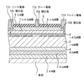
図1は、従来のGaN系HEMTの構造を示す断面図である。SiC基板101上にAlN層102、ノンドープのi−GaN層105、ノンドープのi−AlGaN層106、n型のn−AlGaN層107、及びn型のn−GaN層108が順次形成されている。更に、n−GaN層108上にSiN層109が形成されている。SiN層109に開口部が形成されており、この中にゲート電極111gが形成されている。また、n−GaN層108及びSiN層109に、ゲート電極111gを挟むようにして2個の開口部が形成されており、一方の中にソース電極111sが形成され、他方の中にドレイン電極111dが形成されている。なお、AlN層102はバッファ層として機能する。ゲート電極111gはn−GaN層108にショットキー接触しており、ソース電極111s及びドレイン電極111dはn−AlGaN層107にオーミック接触している。
FIG. 1 is a cross-sectional view showing the structure of a conventional GaN-based HEMT. An
このような従来のGaN系HEMTを高耐圧の電子デバイスに用いる場合、その特性が大きく変動することがある。例えば、高周波パワー動作のオン/オフを繰り返した場合に出力がドリフトすることがある。この現象について説明する。 When such a conventional GaN-based HEMT is used for a high breakdown voltage electronic device, its characteristics may fluctuate greatly. For example, the output may drift when the high frequency power operation is repeatedly turned on / off. This phenomenon will be described.
図2は、GaN系HEMTを備えた回路の構成を示す回路図である。この回路では、トランジスタ(GaN系HEMT)Trのソースが接地され、ドレインにインダクタLの一端及び抵抗素子Rの一端が接続されている。インダクタLの他端には直流バイアスVdが印加される。また、抵抗素子Rの他端は接地される。トランジスタTrのゲートには、−2V〜4Vの交流信号RFを印加する交流電源Pが接続されている。なお、トランジスタTrのゲートには、交流信号RFが印加されないオフ時に−1Vのゲート電圧Vgが印加される。 FIG. 2 is a circuit diagram illustrating a configuration of a circuit including a GaN-based HEMT. In this circuit, the source of a transistor (GaN-based HEMT) Tr is grounded, and one end of an inductor L and one end of a resistance element R are connected to the drain. A DC bias Vd is applied to the other end of the inductor L. The other end of the resistance element R is grounded. An AC power supply P that applies an AC signal RF of −2V to 4V is connected to the gate of the transistor Tr. Note that a gate voltage Vg of −1 V is applied to the gate of the transistor Tr when the AC signal RF is not applied when the transistor Tr is off.
このような回路を基地局用アンプに用いる場合、直流バイアスVdは50V程度に設定され、ドレイン電流の平均値は最大値の2%〜3%程度に設定される。そして、2GHz程度の高周波信号(交流信号RF)をトランジスタTrのゲートに印加すると、図3に示すような電流−電圧特性が得られる。図3中の横軸はドレイン(ドレイン−ソース間)電圧であり、縦軸はドレイン(ドレイン−ソース間)電流である。 When such a circuit is used for the base station amplifier, the DC bias Vd is set to about 50 V, and the average value of the drain current is set to about 2% to 3% of the maximum value. Then, when a high frequency signal (AC signal RF) of about 2 GHz is applied to the gate of the transistor Tr, current-voltage characteristics as shown in FIG. 3 are obtained. The horizontal axis in FIG. 3 is the drain (drain-source) voltage, and the vertical axis is the drain (drain-source) current.
また、基地局用アンプでは、トランジスタTrのオン/オフが頻繁に切り換えられる。例えば、図4(a)に示すような制御を行う。なお、図4中の縦軸はバイアスポイントにおける直流ドレイン電流の値である。また、10mA/mmの設定値は、高周波信号がオフになっている時に流れる予め設定された電流値であり、150mA/mmの平均値は、高周波信号がオンになっている時のドレイン電流の平均値である。 In the base station amplifier, the transistor Tr is frequently turned on / off. For example, control as shown in FIG. Note that the vertical axis in FIG. 4 represents the value of the direct current drain current at the bias point. The set value of 10 mA / mm is a preset current value that flows when the high-frequency signal is off, and the average value of 150 mA / mm is the drain current when the high-frequency signal is on. Average value.
しかしながら、図4(a)に示すような制御を行おうとしても、実際には、図4(b)に示すように、高周波信号をオフにした時に電流が過剰に低下してしまい、次に高周波信号をオンにした時に十分な出力(150mA/mmの電流)を得ることができない。つまり、出力のドリフト現象が生じる。このような過剰な低下により、電流が1mA/mm〜2mA/mm程度となることもある。電流の低下は時間の経過と共に回復するが、出力が安定する程度まで回復させるためには1分間以上の長時間が必要とされる。従って、直流のバイアスが元の状態に戻るまでに、1分間以上の時間が必要となり、高周波信号の断続的なオン/オフの動作が妨げられることがある。図1に示す従来のGaN系HEMTには、このような過度応答特性が存在する。 However, even if the control as shown in FIG. 4A is performed, in practice, as shown in FIG. 4B, when the high-frequency signal is turned off, the current is excessively reduced. When the high frequency signal is turned on, sufficient output (current of 150 mA / mm) cannot be obtained. That is, an output drift phenomenon occurs. Due to such an excessive decrease, the current may be about 1 mA / mm to 2 mA / mm. The decrease in current recovers with the passage of time, but it takes a long time of 1 minute or more to recover the output to a stable level. Therefore, it takes 1 minute or more for the DC bias to return to the original state, and the intermittent on / off operation of the high-frequency signal may be hindered. The conventional GaN-based HEMT shown in FIG. 1 has such transient response characteristics.
このような過度応答特性に伴う出力のドリフト現象を抑制する技術が特許文献2に記載されている。図5は、特許文献2に記載された従来のGaN系HEMTの構造を示す断面図である。このGaN系HEMTでは、図1に示すGaN系HEMTのAlN層102とi−GaN層105との間にAlGaN層103が設けられている。
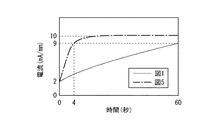
このような図5に示すGaN系HEMTでは、図1に示すGaN系HEMTと比較して、i−GaN層105の結晶性が向上する。このため、i−GaN層105の下部に存在するトラップに捕獲された2次元電子ガスが放出されやすくなり、過度応答特性に伴う出力のドリフト現象が抑制される。図6は、図1に示すGaN系HEMT及び図5に示すGaN系HEMTの出力のドリフト現象を示すグラフであり、図6中の実線が図1に示すGaN系HEMTの特性を示し、一点鎖線が図5に示すGaN系HEMTの特性を示す。高周波信号の印加のオフ時のドレイン電流の設定値が10mA/mmの場合、ドレイン電流が9mA/mm程度まで回復していれば、次の高周波信号を印加しても十分な出力を得ることができる。そして、図6に示すように、高周波信号の印加のオフ時にドレイン電流が2mA/mm程度まで低下したとしても、4秒間程度で9mA/mm程度まで回復する。
In such a GaN-based HEMT shown in FIG. 5, the crystallinity of the i-
また、特許文献3にも、出力のドリフト現象を抑制する技術が開示されている。この技術では、図1に示すGaN系HEMTのAlN層102に相当するAlN層の表面を粗くしている。
特許文献2に記載された技術及び特許文献3に記載された技術によれば所期の目的は達成されるものの、より高速な動作を実現するためには、落ち込んだドレイン電流をより早期に回復させることが要求される。
According to the technique described in
本発明の目的は、オフ時に過剰に落ち込んだドレイン電流をより早期に回復させることができる化合物半導体装置及びその製造方法を提供することにある。 An object of the present invention is to provide a compound semiconductor device and a method for manufacturing the same that can recover a drain current that has dropped excessively at an earlier time.
第1の化合物半導体装置には、基板と、前記基板上に形成された第1のバッファ層と、前記第1のバッファ層上に前記第1のバッファ層と直接接するように形成され、前記第1のバッファ層よりも電子親和力が大きい第2のバッファ層と、前記第2のバッファ層上に前記第2のバッファ層と直接接するように形成され、前記第2のバッファ層よりも電子親和力が小さい第3のバッファ層と、が設けられている。更に、前記第3のバッファ層上方に形成された電子走行層と、前記電子走行層上方に形成された電子供給層と、が設けられている。前記第3のバッファ層と前記電子走行層との界面から前記第1のバッファ層の上面までの距離は12nm〜1000nmである。 The first compound semiconductor device includes a substrate, a first buffer layer formed on the substrate, and a first buffer layer formed on the first buffer layer so as to be in direct contact with the first buffer layer. A second buffer layer having an electron affinity greater than that of the first buffer layer; and a second buffer layer formed on the second buffer layer so as to be in direct contact with the second buffer layer, and having an electron affinity greater than that of the second buffer layer. And a small third buffer layer. Further, an electron transit layer formed on the third buffer layer upper side, and the electron supply layer formed on the electron transit layer above, is provided. The distance from the interface between the third buffer layer and the electron transit layer to the upper surface of the first buffer layer is 12 nm to 1000 nm.
第2の化合物半導体装置には、基板と、前記基板上に形成され、Alを含有する第1のバッファ層と、前記第1のバッファ層上に前記第1のバッファ層と直接接するように形成され、Alを前記第1のバッファ層よりも低濃度で含有する第2のバッファ層と、前記第2のバッファ層上に前記第2のバッファ層と直接接するように形成され、Alを前記第2のバッファ層よりも高濃度で含有する第3のバッファ層と、が設けられている。更に、前記第3のバッファ層上方に形成された電子走行層と、前記電子走行層上方に形成された電子供給層と、が設けられている。前記第3のバッファ層と前記電子走行層との界面から前記第1のバッファ層の上面までの距離は12nm〜1000nmである。 The second compound semiconductor device includes a substrate, a first buffer layer formed on the substrate and containing Al, and formed on the first buffer layer so as to be in direct contact with the first buffer layer. A second buffer layer containing Al at a lower concentration than the first buffer layer, and formed on the second buffer layer so as to be in direct contact with the second buffer layer; And a third buffer layer containing a higher concentration than the second buffer layer. Further, an electron transit layer formed on the third buffer layer upper side, and the electron supply layer formed on the electron transit layer above, is provided. The distance from the interface between the third buffer layer and the electron transit layer to the upper surface of the first buffer layer is 12 nm to 1000 nm.
上記の化合物半導体装置等によれば、適切な第1〜第3のバッファ層により、過度応答特性に伴う出力のドリフト現象をより一層抑制することができる。 According to the above-described compound semiconductor device or the like, the appropriate first to third buffer layers can further suppress the output drift phenomenon associated with the excessive response characteristics.
以下、実施形態について添付の図面を参照しながら具体的に説明する。 Hereinafter, embodiments will be described in detail with reference to the accompanying drawings.
(第1の実施形態)
先ず、第1の実施形態について説明する。図7は、第1の実施形態に係るGaN系HEMT(化合物半導体装置)の構造を示す断面図である。
(First embodiment)
First, the first embodiment will be described. FIG. 7 is a cross-sectional view showing the structure of a GaN-based HEMT (compound semiconductor device) according to the first embodiment.
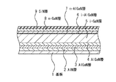
第1の実施形態では、SiC基板等の基板1上に、厚さが5nm〜300nm程度(例えば200nm)のAlN層2が形成されている。AlN層2上に、厚さが10nm〜300nm程度(例えば200nm)のAlGaN層3が形成され、その上に、厚さが2nm〜100nm程度(例えば10nm)のAlGaN層4が形成されている。AlGaN層3の組成はAlx1Ga1-x1Nで表わされ、AlGaN層4の組成はAlx2Ga1-x2Nで表わされる。AlGaN層3の電子親和力はAlN層2及びAlGaN層4の電子親和力よりも大きく、AlN層2の電子親和力はAlGaN層4の電子親和力よりも小さい。x1の値はx2の値よりも小さい。x1の値は0.1〜0.5程度(例えば0.4)であり、x2の値は0.3〜1程度(例えば0.8)である。また、AlGaN層4上に、厚さが200nm〜3000nm程度(例えば800nm)のノンドープのi−GaN層5が形成され、その上に、厚さが0nm〜10nm程度(例えば2nm)のノンドープのi−AlGaN層6が形成され、その上に、厚さが5nm〜50nm程度(例えば20nm)のn型のn−AlGaN層7が形成されている。i−AlGaN層6及びn−AlGaN層7の組成はAlx3Ga1-x3Nで表わされ、x3の値は0.1〜0.4程度(例えば0.2)である。更に、n−AlGaN層7上に、厚さが1nm〜15nm程度(例えば6nm)のn型のn−GaN層8が形成され、その上に、厚さが10nm〜700nm程度(例えば40nm)のSiN層9が形成されている。n−AlGaN層7には、Siが1×1015cm-3〜5×1018cm-3程度(例えば1×1018cm-3)ドーピングされており、n−GaN層8には、Siが1×1015cm-3〜1×1019cm-3程度(例えば5×1018cm-3)ドーピングされている。
In the first embodiment, an
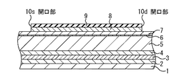
SiN層9には、ゲート電極用の開口部10gが形成されている。また、SiN層9及びn−GaN層8には、開口部10gを間に挟むようにしてソース電極用の開口部10s、及びドレイン電極用の開口部10dが形成されている。そして、開口部10g内にゲート電極11gが形成され、開口部10s内にソース電極11sが形成され、開口部10d内にドレイン電極11dが形成されている。ゲート電極11gは、例えばNi膜とその上に形成されたAu膜とから構成されている。また、ソース電極11s及びドレイン電極11dは、例えば、Ta膜とその上に形成されたAl膜とから構成されている。ゲート電極11gはn−GaN層8にショットキー接触しており、ソース電極11s及びドレイン電極11dはn−AlGaN層7にオーミック接触している。
In the
なお、基板1の表面側から見たレイアウトは、例えば図8のようになる。つまり、ゲート電極11g、ソース電極11s及びドレイン電極11dの平面形状が櫛歯状となっており、ソース電極11s及びドレイン電極11dが交互に配置されている。そして、これらの間にゲート電極11gが配置されている。このようなマルチフィンガーゲート構造を採用することにより、出力を向上させることができる。なお、図7に示す断面図は、図8中のI−I線に沿った断面図である。また、活性領域10にはAlN層2、AlGaN層3、AlGaN層4及びi−GaN層5等が含まれており、活性領域10の周囲はイオン注入又はメサエッチング等により不活性領域とされている。
The layout viewed from the front side of the
このような第1の実施形態では、格子不整合に起因するピエゾ効果により、i−GaN層5のi−AlGaN層6との界面近傍に電子が誘起される。この結果、2次元電子ガス層(2DEG)が現れ、この部分が電子走行層として機能する。また、i−AlGaN層6及びn−AlGaN層7が電子供給層として機能する。
In the first embodiment, electrons are induced in the vicinity of the interface between the i-
また、AlN層2、AlGaN層3及びAlGaN層4がバッファ層として機能する。そして、これらのバッファ層の組み合わせにより、i−GaN層5の表層部に誘起された電子が、i−GaN層5の下部に存在するトラップまで到達しにくくなる。
Further, the
ここで、電子がi−GaN層5の下部に存在するトラップまで到達しにくくなる理由について説明する。図9は、第1の実施形態におけるバンド構造及び電荷密度を示す図であり、図10は、図1に示す従来のGaN系HEMTにおけるバンド構造及び電荷密度を示す図である。なお、図9(b)は図9(a)中の深さが極浅い部分を拡大して示しており、図10(b)は図10(a)中の深さが極浅い部分を拡大して示している。
Here, the reason why it becomes difficult for electrons to reach the traps existing under the i-
図9と図10とを比較すると分かるように、基板1の伝導帯と基板101の伝導帯とは、ほぼ互いに同等である。また、i−GaN層5、i−AlGaN層6、n−AlGaN層7、及びn−GaN層8の伝導帯とi−GaN層105、i−AlGaN層106、n−AlGaN層107、及びn−GaN層108の伝導帯も、ほぼ互いに同等である。ところが、第1の実施形態では、AlN層2の直上に位置するAlGaN層3の伝導帯が5.0eV程度であるのに対し、従来のGaN系HEMTでは、AlN層102の直上に位置するi−GaN層105の伝導帯が3.5eV程度である。AlGaN層3及び4の界面近傍にピエゾ電荷及び自然分極電荷が強く誘引されるからである。更に、第1の実施形態では、AlGaN層4の伝導帯が高いため、AlGaN層4が電子のAlN層2に向かう移動のバリアとして機能する。
As can be seen by comparing FIG. 9 and FIG. 10, the conduction band of the
これらの理由から、第1の実施形態では、深さが600nm〜700nm程度の領域で電子の密度が、急激に減少にしているのに対し、従来のGaN系HEMTでは、電子の密度はなだらかに減少しているに過ぎないのである。このことは、電子がi−GaN層5の下部に存在するトラップまで到達しにくくなっていることを意味する。そして、電子がトラップまで到達しにくいため、過度応答特性に伴う出力のドリフト現象が低減される。即ち、図11に示すように、オンからオフに切り換えられた際のドレイン電流の落ち込みが少ない。従って、落ち込んだドレイン電流がより早期に回復し、より高速な動作が可能となる。
For these reasons, in the first embodiment, the electron density is drastically decreased in the region having a depth of about 600 nm to 700 nm, whereas in the conventional GaN-based HEMT, the electron density is gentle. It is only decreasing. This means that it is difficult for electrons to reach the traps existing under the i-
なお、AlGaN層3におけるAlの割合x1は、0.1〜0.5であることが好ましい。割合x1が0.1未満であると、AlGaN層4の伝導帯を十分に引き上げることが困難になることがあり、割合x1が0.5を超えると、歪み及び反りが生じやすくなるからである。また、AlGaN層4におけるAlの割合x2は、0.3以上であることが好ましい。割合x2が0.3未満であると、AlGaN層4自身の伝導帯が十分に高いものとなりにくいからである。また、AlN層2の電子親和力はAlGaN層4の電子親和力よりも小さいことが好ましい。これは、AlGaN層4の電子親和力がAlN層2の電子親和力以下であると、電子の移動を抑制する効果が低下して過度応答特性の抑制が不十分になりやすいからである。
The Al ratio x1 in the
また、AlGaN層3が設けられておらずに、Alの割合が高いAlGaN層4がAlN層2上に直接設けられている場合には、AlGaN層3におけるAlの割合x1が0.5を超える場合と同様に、歪み及び反りが生じやすくなる。更に、AlGaN層4の伝導帯が十分に引き上げられず、ドレイン電流を十分に低減することが困難になる。従って、Alの割合が比較的低いAlGaN層3は必須である。
Further, when the
なお、抵抗体及びキャパシタ等をも実装してモノリシックマイクロ波集積回路(MMIC)としてもよい。 Note that a resistor, a capacitor, and the like may be mounted to form a monolithic microwave integrated circuit (MMIC).
次に、第1の実施形態に係るGaN系HEMT(化合物半導体装置)を製造する方法について説明する。図12A乃至図12Eは、第1の実施形態に係るGaN系HEMT(化合物半導体装置)の製造方法を工程順に示す断面図である。 Next, a method for manufacturing a GaN-based HEMT (compound semiconductor device) according to the first embodiment will be described. 12A to 12E are cross-sectional views illustrating a method of manufacturing a GaN-based HEMT (compound semiconductor device) according to the first embodiment in the order of steps.
第1の実施形態では、先ず、図12Aに示すように、基板1上に、夫々バッファ層として、AlN層2、AlGaN層3、及びAlGaN層4をこの順で形成する。更に、AlGaN層4上にi−GaN層5を形成する。次いで、i−GaN層5上に、i−AlGaN層6、n−AlGaN層7、及びn−GaN層8をこの順で形成する。AlN層2、AlGaN層3、AlGaN層4、i−GaN層5、i−AlGaN層6、n−AlGaN層7、及びn−GaN層8の形成は、例えば有機金属気相成長(MOVPE)法等の結晶成長法により行う。この場合、原料ガスを選択することにより、これらの層を連続して形成することができる。アルミニウム(Al)の原料、ガリウム(Ga)の原料、インジウム(In)の原料としては、例えば、夫々トリメチルアルミニウム、トリメチルガリウム、トリメチルインジウムを使用することができる。また、窒素(N)の原料として、例えばアンモニア(NH3)を使用することができる。また、n−AlGaN層7及びn−GaN層8に不純物として含まれるシリコン(Si)の原料としては、例えばシラン(SiH4)を使用することができる。
In the first embodiment, first, as shown in FIG. 12A, an
特に、AlGaN層3の形成の際には、例えば成長温度1000℃、成長圧力90torrの雰囲気で、トリメチルアルミニウムを20sccm、トリメチルガリウムを30sccm、アンモニアを5SLM、水素を25SLM流す。この場合、例えばAlの割合x1が0.4程度のAlGaN層3が得られる。また、AlGaN層4の形成の際には、例えば成長温度1000℃、成長圧力90torrの雰囲気で、トリメチルアルミニウムを30sccm、トリメチルガリウムを20sccm、アンモニアを5SLM、水素を25SLM流す。この場合、例えばAlの割合x2が0.8程度のAlGaN層4が得られる。
In particular, when the
n−GaN層8の形成後には、その上にSiN層9を、例えばプラズマCVD(chemical vapor deposition)法により形成する。
After the n-
次いで、SiN層9上に、ソース電極11s及びドレイン電極11dを形成する予定の領域を開口するレジストパターンを形成する。その後、レジストパターンをマスクとして用いて、SiN層9及びn−GaN層8のエッチングを行うことにより、図12Bに示すように、SiN層9及びn−GaN層8に、ソース電極用の開口部10s及びドレイン電極用の開口部10dを形成する。このエッチングとしては、例えば塩素系ガスを用いたドライエッチングを行う。なお、開口部10s及び10dの深さに関し、n−GaN層8の一部を残してもよく、また、n−AlGaN層7の一部を除去してもよい。つまり、開口部10s及び10dの深さがSiN層9及びn−GaN層8の総厚と一致している必要はない。
Next, a resist pattern is formed on the
続いて、図12Cに示すように、開口部10s及び10d内に、夫々ソース電極11s及びドレイン電極11dをリフトオフ法により形成する。ソース電極11s及びドレイン電極11dの形成では、開口部10s及び10dを形成する際に用いたレジストパターンを除去した後、ソース電極11s及びドレイン電極11dを形成する領域を開口する新たなレジストパターンを形成し、Ta及びAlの蒸着を行い、その後、レジストパターン上に付着したTa及びAlをレジストパターンごと除去する。Ta膜、Al膜の厚さは、例えば、夫々30nm程度、200nm程度とする。そして、窒素雰囲気中で400℃〜1000℃、例えば600℃で熱処理を行い、オーミック特性を確立する。
Subsequently, as shown in FIG. 12C, a
ソース電極11s及びドレイン電極11dの形成後、開口部10gを形成する予定の領域を開口するレジストパターンを形成する。次いで、レジストパターンを用いたエッチングを行うことにより、図12Dに示すように、SiN層9に開口部10gを形成する。このエッチングとしては、例えば酸を用いたウェットエッチングを行う。そして、レジストパターンを除去する。このようなエッチングでは、n−GaN層8はエッチングされないため、ウェハ面内で均一なエッチングが可能である。
After the formation of the
その後、図12Eに示すように、開口部10g内に、ゲート電極11gをリフトオフ法により形成する。ゲート電極11gの形成では、開口部10gを形成する際に用いたレジストパターンを除去した後、ゲート電極11gを形成する領域を開口する新たなレジストパターンを形成し、Ni及びAuの蒸着を行い、その後、レジストパターン上に付着したNi及びAuをレジストパターンごと除去する。Ni膜、Au膜の厚さは、例えば、夫々30nm程度、400nm程度とする。
Thereafter, as shown in FIG. 12E, a gate electrode 11g is formed in the
このような製造方法により、図7に示す構造のGaN系HEMTを得ることができる。 With such a manufacturing method, a GaN-based HEMT having the structure shown in FIG. 7 can be obtained.
なお、ゲート電極11gのゲート長、即ちソース電極11sとドレイン電極11dとを結ぶ方向の長さは、0.05μm〜2μm程度(例えば0.5μm)である。また、ユニットゲート幅、即ちゲート長の方向に直交する方向の長さは、50μm〜800μm程度(例えば400μm)である。
The gate length of the gate electrode 11g, that is, the length in the direction connecting the
(第2の実施形態)
次に、第2の実施形態について説明する。図13は、第2の実施形態に係るGaN系HEMT(化合物半導体装置)の構造を示す断面図である。
(Second Embodiment)
Next, a second embodiment will be described. FIG. 13 is a cross-sectional view showing the structure of a GaN-based HEMT (compound semiconductor device) according to the second embodiment.
第2の実施形態では、第1の実施形態におけるAlGaN層3に代わって、厚さが10nm〜500nm程度(例えば300nm)のノンドープのInAlN層13が設けられ、AlGaN層4に代わって、厚さが5nm〜500nm程度(例えば100nm)のInAlN層14が設けられている。InAlN層13の組成はIny1Al1-y1Nで表わされ、InAlN層14の組成はIny2Al1-y2Nで表わされる。InAlN層13の電子親和力はAlN層2及びInAlN層14の電子親和力よりも大きく、AlN層2の電子親和力はInAlN層14の電子親和力よりも小さい。y1の値はy2の値よりも大きい。y1の値は0.1〜0.25程度(例えば0.23)であり、y2の値は0.1〜0.25程度(例えば0.15)である。
In the second embodiment, a
他の構成は第1の実施形態と同様である。 Other configurations are the same as those of the first embodiment.
このような第2の実施形態によっても第1の実施形態と同様の効果を得ることができる。図14は、第2の実施形態におけるバンド構造及び電荷密度を示す図である。なお、図14(b)は図14(a)中の深さが極浅い部分を拡大して示している。 The effect similar to 1st Embodiment can be acquired also by such 2nd Embodiment. FIG. 14 is a diagram showing a band structure and a charge density in the second embodiment. In addition, FIG.14 (b) has expanded and shown the part whose depth in FIG.14 (a) is very shallow.
第2の実施形態では、AlN層2の直上に位置するInAlN層13の伝導帯が4.0eVを超えている。このため、第2の実施形態でも、深さが600nm〜700nm程度の領域で電子の密度が、急激に減少にしている。従って、第1の実施形態と同様に、過度応答特性に伴う出力のドリフト現象が低減される。即ち、図15に示すように、オンからオフに切り換えられた際のドレイン電流の落ち込みが少ない。従って、落ち込んだドレイン電流がより早期に回復し、より高速な動作が可能となる。
In the second embodiment, the conduction band of the
また、図16に示すように、第1の実施形態でバッファ層に用いられているAlGaNの格子定数はGaNの格子定数よりも小さくなるが、第2の実施形態でバッファ層に用いられているInAlNの格子定数はIn及びAlの割合によってGaNの格子定数より大きくなることがある。例えば、InAlN層13におけるInの割合y1が0.23の場合、その格子定数はGaNのものより大きくなり、InAlN層14におけるInの割合y2が0.15の場合、その格子定数はGaNのものより小さくなる。従って、InAlN層13及び14の間の格子定数の差を大きくしても歪みが生じにくい。このため、InAlN層14をAlGaN層4よりも厚くして、伝導帯をより引き上げ、電子をより一層トラップまで到達しにくくすることができる。更に、In及びAlの間の格子定数の差は、Al及びGaの間の格子定数の差よりも大きい。このため自然分極がより強く誘引され、この点でも電子をより一層トラップまで到達しにくくすることができる。
Also, as shown in FIG. 16, the lattice constant of AlGaN used in the buffer layer in the first embodiment is smaller than the lattice constant of GaN, but is used in the buffer layer in the second embodiment. The lattice constant of InAlN may be larger than that of GaN depending on the ratio of In and Al. For example, when the In ratio y1 in the
なお、InAlN層13及びInAlN層14におけるInの割合y1及びy2は、0.1〜0.25であることが好ましい。割合y1及びy2が0.1未満であると、InAlN層14の伝導帯を十分に引き上げることが困難になることがあり、割合y1及びy2が0.25を超えるInAlN層は形成が困難だからである。
The In ratios y1 and y2 in the
また、第2の実施形態に係るGaN系HEMTを製造する際には、第1の実施形態におけるAlGaN層3及び4の形成に代えて、InAlN層13及び14を形成すればよい。In原料にはトリメチルインジウムを用いる。成長温度は950℃とAlGaNよりも低温化させる。これはInの脱離を抑制するためである。例えばInAlN層13の形成の際には、例えば成長温度950℃、成長圧力90torrの雰囲気で、トリメチルインジウムを150sccm、トリメチルガリウムを30sccm、アンモニアを5SLM、水素を25SLM流す。この場合、例えばInの割合が0.23程度のInAlN層13が得られる。また、InAlN層14の形成の際には、例えば成長温度950℃、成長圧力90torrの雰囲気で、トリメチルインジウムを100sccm、トリメチルガリウムを20sccm、アンモニアを5SLM、水素を25SLM流す。この場合、例えばInの割合が0.15のInAlN層14が得られる。
Further, when manufacturing the GaN-based HEMT according to the second embodiment, InAlN layers 13 and 14 may be formed instead of forming the AlGaN layers 3 and 4 in the first embodiment. Trimethylindium is used as the In raw material. The growth temperature is 950 ° C., which is lower than that of AlGaN. This is to suppress the desorption of In. For example, when the
なお、いずれの実施形態においても、基板1として、炭化シリコン(SiC)基板、サファイア基板、シリコン基板、GaN基板又はGaAs基板等を用いてもよい。基板1が、導電性、半絶縁性又は絶縁性のいずれであってもよい。
In any of the embodiments, a silicon carbide (SiC) substrate, a sapphire substrate, a silicon substrate, a GaN substrate, a GaAs substrate, or the like may be used as the
また、ゲート電極11g、ソース電極11s及びドレイン電極11dの構造は上述の実施形態のものに限定されない。例えば、これらが単層から構成されていてもよい。また、これらの形成方法はリフトオフ法に限定されない。更に、オーミック特性が得られるのであれば、ソース電極11s及びドレイン電極11dの形成後の熱処理を省略してもよい。また、ゲート電極11gに対して熱処理を行ってもよい。
Further, the structures of the gate electrode 11g, the
また、各層の厚さ及び材料等も上述の実施形態のものに限定されない。例えば、InAlGaN等がバッファ層に用いられていてもよい。また、第1の実施形態におけるAlGaN層3と第2の実施形態におけるInAlN層14とが組み合わされていてもよい。
Further, the thickness and material of each layer are not limited to those of the above-described embodiment. For example, InAlGaN or the like may be used for the buffer layer. Further, the
また、第1及び第2の実施形態において、n−GaN層8のゲート電極11gが接している部分がエッチングされていてもよい。その深さはn−GaN層8の厚さと一致していてもよく、それよりも浅くてもよい。但し、このエッチングは、均一に行うことが好ましい。
In the first and second embodiments, the portion of the n-
また、第1及び第2の実施形態において、第3のバッファ層上に第4のバッファ層が形成されていてもよい。この場合、第4のバッファ層の電子親和力は、第3のバッファ層の電子親和力よりも大きいことが好ましい。このような第4のバッファ層が設けられていると、電子走行層の結晶性がより一層向上する。第4のバッファ層としては、例えば第2のバッファ層と同様のものを用いることができる。つまり、第1の実施形態では、例えばAlGaN層3と同様の組成のAlGaN層を用いることができ、第2の実施形態では、例えばInAlN層13と同様の組成のInAlN層を用いることができる。
In the first and second embodiments, a fourth buffer layer may be formed on the third buffer layer. In this case, the electron affinity of the fourth buffer layer is preferably larger than the electron affinity of the third buffer layer. When such a fourth buffer layer is provided, the crystallinity of the electron transit layer is further improved. As the fourth buffer layer, for example, a layer similar to the second buffer layer can be used. That is, in the first embodiment, for example, an AlGaN layer having the same composition as that of the
以下、本発明の諸態様を付記としてまとめて記載する。 Hereinafter, various aspects of the present invention will be collectively described as supplementary notes.
(付記1)
基板と、
前記基板上に形成された第1のバッファ層と、
前記第1のバッファ層上に形成され、前記第1のバッファ層よりも電子親和力が大きい第2のバッファ層と、
前記第2のバッファ層上に形成され、前記第2のバッファ層よりも電子親和力が小さい第3のバッファ層と、
前記第3のバッファ層上方に形成された電子走行層と、
前記電子走行層上方に形成された電子供給層と、
を有することを特徴とする化合物半導体装置。
(Appendix 1)
A substrate,
A first buffer layer formed on the substrate;
A second buffer layer formed on the first buffer layer and having a higher electron affinity than the first buffer layer;
A third buffer layer formed on the second buffer layer and having a lower electron affinity than the second buffer layer;
An electron transit layer formed above the third buffer layer;
An electron supply layer formed above the electron transit layer;
A compound semiconductor device comprising:
(付記2)
前記第1のバッファ層の電子親和力は、前記第3のバッファ層の電子親和力も小さいことを特徴とする付記1に記載の化合物半導体装置。
(Appendix 2)
The compound semiconductor device according to
(付記3)
前記第1のバッファ層、前記第2のバッファ層及び前記第3のバッファ層は、窒化物半導体から構成されていることを特徴とする付記1又は2に記載の化合物半導体装置。
(Appendix 3)
The compound semiconductor device according to
(付記4)
前記第1のバッファ層、前記第2のバッファ層及び前記第3のバッファ層は、少なくともAlを含有することを特徴とする付記1乃至3のいずれか1項に記載の化合物半導体装置。
(Appendix 4)
4. The compound semiconductor device according to any one of
(付記5)
前記第2のバッファ層の組成は、Alx1Ga1-x1N(0.1≦x1≦0.5)で表わされ、
前記第3のバッファ層の組成は、Alx2Ga1-x2N(0.3≦x2≦1)で表わされ、
x1の値はx2の値よりも小さいことを特徴とする付記1乃至4のいずれか1項に記載の化合物半導体装置。
(Appendix 5)
The composition of the second buffer layer is represented by Al x1 Ga 1-x1 N (0.1 ≦ x1 ≦ 0.5),
The composition of the third buffer layer is represented by Al x2 Ga 1-x2 N (0.3 ≦ x2 ≦ 1),
5. The compound semiconductor device according to any one of
(付記6)
前記第2のバッファ層の組成は、Iny1Al1-y1N(0.1≦y1≦0.25)で表わされ、
前記第3のバッファ層の組成は、Iny2Al1-y2N(0.1≦y2≦0.25)で表わされ、
y1の値はy2の値よりも大きいことを特徴とする付記1乃至4のいずれか1項に記載の化合物半導体装置。
(Appendix 6)
The composition of the second buffer layer is represented by In y1 Al 1-y1 N (0.1 ≦ y1 ≦ 0.25),
The composition of the third buffer layer is represented by In y2 Al 1-y2 N (0.1 ≦ y2 ≦ 0.25),
5. The compound semiconductor device according to any one of
(付記7)
前記第2のバッファ層の格子定数はGaNの格子定数よりも大きく、
前記第3のバッファ層の格子定数はGaNの格子定数よりも小さいことを特徴とする付記6に記載の化合物半導体装置。
(Appendix 7)
The lattice constant of the second buffer layer is larger than the lattice constant of GaN,
The compound semiconductor device according to
(付記8)
前記第2のバッファ層の組成は、Iny1Al1-y1N(0.1≦y1≦0.25)で表わされ、
前記第3のバッファ層の組成は、Alx2Ga1-x2N(0.3≦x2≦1)で表わされることを特徴とする付記1乃至4のいずれか1項に記載の化合物半導体装置。
(Appendix 8)
The composition of the second buffer layer is represented by In y1 Al 1-y1 N (0.1 ≦ y1 ≦ 0.25),
5. The compound semiconductor device according to
(付記9)
前記第1のバッファ層の組成は、AlNで表わされることを特徴とする付記1乃至8のいずれか1項に記載の化合物半導体装置。
(Appendix 9)
9. The compound semiconductor device according to any one of
(付記10)
前記第3のバッファ層と前記電子走行層との間に配置され、前記第3のバッファ層よりも電子親和力が大きい第4のバッファ層を更に有することを特徴とする付記1乃至9のいずれか1項に記載の化合物半導体装置。
(Appendix 10)
The third is disposed between the buffer layer and the electron transit layer, any of
(付記11)
基板と、
前記基板上に形成され、Alを含有する第1のバッファ層と、
前記第1のバッファ層上に形成され、Alを前記第1のバッファ層よりも低濃度で含有する第2のバッファ層と、
前記第2のバッファ層上に形成され、Alを前記第2のバッファ層よりも高濃度で含有する第3のバッファ層と、
前記第3のバッファ層上方に形成された電子走行層と、
前記電子走行層上方に形成された電子供給層と、
を有することを特徴とする化合物半導体装置。
(Appendix 11)
A substrate,
A first buffer layer formed on the substrate and containing Al;
A second buffer layer formed on the first buffer layer and containing Al at a lower concentration than the first buffer layer;
A third buffer layer formed on the second buffer layer and containing Al at a higher concentration than the second buffer layer;
An electron transit layer formed above the third buffer layer;
An electron supply layer formed above the electron transit layer;
A compound semiconductor device comprising:
(付記12)
前記第3のバッファ層と前記電子走行層との間に配置され、前記第3のバッファ層よりも電子親和力が大きい第4のバッファ層を更に有することを特徴とする付記11に記載の化合物半導体装置。
(Appendix 12)
The compound semiconductor according to
(付記13)
基板上に第1のバッファ層を形成する工程と、
前記第1のバッファ層上に、前記第1のバッファ層よりも電子親和力が大きい第2のバッファ層を形成する工程と、
前記第2のバッファ層上に、前記第2のバッファ層よりも電子親和力が小さい第3のバッファ層を形成する工程と、
前記第3のバッファ層上方に電子走行層を形成する工程と、
前記電子走行層上方に電子供給層を形成する工程と、
を有することを特徴とする化合物半導体装置の製造方法。
(Appendix 13)
Forming a first buffer layer on the substrate;
Forming a second buffer layer having a higher electron affinity than the first buffer layer on the first buffer layer;
Forming a third buffer layer having a lower electron affinity than the second buffer layer on the second buffer layer;
Forming an electron transit layer above the third buffer layer;
Forming an electron supply layer above the electron transit layer;
A method for producing a compound semiconductor device, comprising:
(付記14)
前記第3のバッファ層を形成する工程と前記電子走行層を形成する工程との間に、前記第3のバッファ層よりも電子親和力が大きい第4のバッファ層を形成する工程を更に有することを特徴とする付記13に記載の化合物半導体装置の製造方法。
(Appendix 14)
The method further includes the step of forming a fourth buffer layer having an electron affinity greater than that of the third buffer layer between the step of forming the third buffer layer and the step of forming the electron transit layer. 14. A method for manufacturing a compound semiconductor device according to
(付記15)
前記第1のバッファ層、前記第2のバッファ層及び前記第3のバッファ層として、窒化物半導体から構成されるものを形成することを特徴とする付記13又は14に記載の化合物半導体装置の製造方法。
(Appendix 15)
15. The compound semiconductor device according to
(付記16)
前記第1のバッファ層、前記第2のバッファ層及び前記第3のバッファ層として、少なくともAlを含有するものを形成することを特徴とする付記13乃至15のいずれか1項に記載の化合物半導体装置の製造方法。
(Appendix 16)
16. The compound semiconductor according to any one of
(付記17)
前記第2のバッファ層として、組成がAlx1Ga1-x1N(0.1≦x1≦0.5)で表わされるものを形成し、
前記第3のバッファ層として、組成がAlx2Ga1-x2N(0.3≦x2≦1)で表わされるものを形成し、
x1の値はx2の値よりも小さいことを特徴とする付記13乃至16のいずれか1項に記載の化合物半導体装置の製造方法。
(Appendix 17)
Forming the second buffer layer having a composition represented by Al x1 Ga 1-x1 N (0.1 ≦ x1 ≦ 0.5);
Forming the third buffer layer having a composition represented by Al x2 Ga 1-x2 N (0.3 ≦ x2 ≦ 1);
17. The method for manufacturing a compound semiconductor device according to any one of
(付記18)
前記第2のバッファ層として、組成がIny1Al1-y1N(0.1≦y1≦0.25)で表わされるものを形成し、
前記第3のバッファ層として、組成がIny2Al1-y2N(0.1≦y2≦0.25)で表わされるものを形成し、
y1の値はy2の値よりも大きいことを特徴とする付記13乃至16のいずれか1項に記載の化合物半導体装置の製造方法。
(Appendix 18)
Forming the second buffer layer having a composition represented by In y1 Al 1-y1 N (0.1 ≦ y1 ≦ 0.25);
Forming the third buffer layer having a composition represented by In y2 Al 1-y2 N (0.1 ≦ y2 ≦ 0.25);
17. The method for manufacturing a compound semiconductor device according to any one of
(付記19)
前記第2のバッファ層として、格子定数がGaNの格子定数よりも大きいものを形成し、
前記第3のバッファ層として、格子定数がGaNの格子定数よりも小さいものを形成することを特徴とする付記18に記載の化合物半導体装置の製造方法。
(Appendix 19)
As the second buffer layer, a layer having a lattice constant larger than that of GaN is formed,
19. The method of manufacturing a compound semiconductor device according to
(付記20)
基板上に、Alを含有する第1のバッファ層を形成する工程と、
前記第1のバッファ層上に、Alを前記第1のバッファ層よりも低濃度で含有する第2のバッファ層を形成する工程と、
前記第2のバッファ層上に、Alを前記第2のバッファ層よりも高濃度で含有する第3のバッファ層を形成する工程と、
前記第3のバッファ層上方に電子走行層を形成する工程と、
前記電子走行層上方に電子供給層を形成する工程と、
を有することを特徴とする化合物半導体装置の製造方法。
(Appendix 20)
Forming a first buffer layer containing Al on the substrate;
Forming a second buffer layer containing Al at a lower concentration than the first buffer layer on the first buffer layer;
Forming a third buffer layer containing Al at a higher concentration than the second buffer layer on the second buffer layer;
Forming an electron transit layer above the third buffer layer;
Forming an electron supply layer above the electron transit layer;
A method for producing a compound semiconductor device, comprising:
1:基板
2:AlN層
3、4:AlGaN層
5:i−GaN層
6:i−AlGaN層
7:n−AlGaN層
8:n−GaN層
9:SiN層
10:活性領域
10g、10s、10d:開口部
11d:ドレイン電極
11g:ゲート電極
11s:ソース電極
13、14:InAlN層
1: substrate 2:
Claims (10)
前記基板上に形成された第1のバッファ層と、
前記第1のバッファ層上に前記第1のバッファ層と直接接するように形成され、前記第1のバッファ層よりも電子親和力が大きい第2のバッファ層と、
前記第2のバッファ層上に前記第2のバッファ層と直接接するように形成され、前記第2のバッファ層よりも電子親和力が小さい第3のバッファ層と、
前記第3のバッファ層上方に形成された電子走行層と、
前記電子走行層上方に形成された電子供給層と、
を有し、
前記第3のバッファ層と前記電子走行層との界面から前記第1のバッファ層の上面までの距離は12nm〜1000nmであることを特徴とする化合物半導体装置。 A substrate,
A first buffer layer formed on the substrate;
A second buffer layer formed on the first buffer layer so as to be in direct contact with the first buffer layer and having a higher electron affinity than the first buffer layer;
A third buffer layer formed on the second buffer layer so as to be in direct contact with the second buffer layer and having an electron affinity smaller than that of the second buffer layer;
An electron transit layer formed above the third buffer layer;
An electron supply layer formed above the electron transit layer;
I have a,
It said third distance buffer layer from the interface between the electron transit layer to the top surface of the first buffer layer is a compound semiconductor device according to claim 12nm~1000nm der Rukoto.
前記第3のバッファ層の組成は、Alx2Ga1-x2 Nで表わされ、
x1の値はx2の値よりも小さいことを特徴とする請求項1乃至4のいずれか1項に記載の化合物半導体装置。 The composition of the second buffer layer is represented by Al x1 Ga 1-x1 N ,
The composition of the third buffer layer is represented by Al x2 Ga 1-x2 N ,
5. The compound semiconductor device according to claim 1, wherein a value of x1 is smaller than a value of x2.
前記第3のバッファ層の組成は、Iny2Al1-y2 Nで表わされ、
y1の値はy2の値よりも大きいことを特徴とする請求項1乃至4のいずれか1項に記載の化合物半導体装置。 The composition of the second buffer layer is represented by In y1 Al 1-y1 N ,
The composition of the third buffer layer is represented by In y2 Al 1-y2 N ,
5. The compound semiconductor device according to claim 1, wherein the value of y <b> 1 is larger than the value of y <b> 2.
前記第3のバッファ層の格子定数はGaNの格子定数よりも小さいことを特徴とする請求項6に記載の化合物半導体装置。 The lattice constant of the second buffer layer is larger than the lattice constant of GaN,
The compound semiconductor device according to claim 6, wherein a lattice constant of the third buffer layer is smaller than a lattice constant of GaN.
前記基板上に形成され、Alを含有する第1のバッファ層と、
前記第1のバッファ層上に前記第1のバッファ層と直接接するように形成され、Alを前記第1のバッファ層よりも低濃度で含有する第2のバッファ層と、
前記第2のバッファ層上に前記第2のバッファ層と直接接するように形成され、Alを前記第2のバッファ層よりも高濃度で含有する第3のバッファ層と、
前記第3のバッファ層上方に形成された電子走行層と、
前記電子走行層上方に形成された電子供給層と、
を有し、
前記第3のバッファ層と前記電子走行層との界面から前記第1のバッファ層の上面までの距離は12nm〜1000nmであることを特徴とする化合物半導体装置。 A substrate,
A first buffer layer formed on the substrate and containing Al;
A second buffer layer formed on the first buffer layer so as to be in direct contact with the first buffer layer and containing Al at a lower concentration than the first buffer layer;
A third buffer layer formed on the second buffer layer so as to be in direct contact with the second buffer layer and containing Al at a higher concentration than the second buffer layer;
An electron transit layer formed above the third buffer layer;
An electron supply layer formed above the electron transit layer;
I have a,
It said third distance buffer layer from the interface between the electron transit layer to the top surface of the first buffer layer is a compound semiconductor device according to claim 12nm~1000nm der Rukoto.
前記第1のバッファ層上に、前記第1のバッファ層よりも電子親和力が大きい第2のバッファ層を前記第1のバッファ層と直接接するように形成する工程と、
前記第2のバッファ層上に、前記第2のバッファ層よりも電子親和力が小さい第3のバッファ層を前記第2のバッファ層と直接接するように形成する工程と、
前記第3のバッファ層上方に電子走行層を形成する工程と、
前記電子走行層上方に電子供給層を形成する工程と、
を有し、
前記第3のバッファ層と前記電子走行層との界面から前記第1のバッファ層の上面までの距離は12nm〜1000nmであることを特徴とする化合物半導体装置の製造方法。 Forming a first buffer layer on the substrate;
Forming on the first buffer layer a second buffer layer having a higher electron affinity than the first buffer layer so as to be in direct contact with the first buffer layer ;
Forming a third buffer layer having an electron affinity smaller than that of the second buffer layer on the second buffer layer so as to be in direct contact with the second buffer layer ;
Forming an electron transit layer above the third buffer layer;
Forming an electron supply layer above the electron transit layer;
I have a,
Manufacturing method of the third of the distance buffer layer from the interface between the electron transit layer to the top surface of the first buffer layer is a compound semiconductor device according to claim 12nm~1000nm der Rukoto.
Priority Applications (5)
| Application Number | Priority Date | Filing Date | Title |
|---|---|---|---|
| JP2009023953A JP5487631B2 (en) | 2009-02-04 | 2009-02-04 | Compound semiconductor device and manufacturing method thereof |
| US12/697,391 US8294181B2 (en) | 2009-02-04 | 2010-02-01 | Compound semiconductor device and method of manufacturing the same |
| CN2010101110119A CN101794815B (en) | 2009-02-04 | 2010-02-02 | Compound semiconductor device and manufacturing method thereof |
| EP10152567.3A EP2216806B1 (en) | 2009-02-04 | 2010-02-03 | Compound semiconductor device and method of manufacturing the same |
| US13/591,401 US8507329B2 (en) | 2009-02-04 | 2012-08-22 | Compound semiconductor device and method of manufacturing the same |
Applications Claiming Priority (1)
| Application Number | Priority Date | Filing Date | Title |
|---|---|---|---|
| JP2009023953A JP5487631B2 (en) | 2009-02-04 | 2009-02-04 | Compound semiconductor device and manufacturing method thereof |
Publications (2)
| Publication Number | Publication Date |
|---|---|
| JP2010182812A JP2010182812A (en) | 2010-08-19 |
| JP5487631B2 true JP5487631B2 (en) | 2014-05-07 |
Family
ID=42136333
Family Applications (1)
| Application Number | Title | Priority Date | Filing Date |
|---|---|---|---|
| JP2009023953A Active JP5487631B2 (en) | 2009-02-04 | 2009-02-04 | Compound semiconductor device and manufacturing method thereof |
Country Status (4)
| Country | Link |
|---|---|
| US (2) | US8294181B2 (en) |
| EP (1) | EP2216806B1 (en) |
| JP (1) | JP5487631B2 (en) |
| CN (1) | CN101794815B (en) |
Families Citing this family (41)
| Publication number | Priority date | Publication date | Assignee | Title |
|---|---|---|---|---|
| AU2010281317A1 (en) | 2009-08-04 | 2012-02-23 | Gan Systems Inc. | Island matrixed gallium nitride microwave and power switching transistors |
| US9818857B2 (en) | 2009-08-04 | 2017-11-14 | Gan Systems Inc. | Fault tolerant design for large area nitride semiconductor devices |
| US9029866B2 (en) * | 2009-08-04 | 2015-05-12 | Gan Systems Inc. | Gallium nitride power devices using island topography |
| US8791508B2 (en) * | 2010-04-13 | 2014-07-29 | Gan Systems Inc. | High density gallium nitride devices using island topology |
| JP2012054471A (en) * | 2010-09-02 | 2012-03-15 | Fujitsu Ltd | Semiconductor device, method of manufacturing the same, and power supply device |
| JP5672926B2 (en) * | 2010-10-08 | 2015-02-18 | 富士通株式会社 | Compound semiconductor device and manufacturing method thereof |
| KR101720589B1 (en) * | 2010-10-11 | 2017-03-30 | 삼성전자주식회사 | E-mode High Electron Mobility Transistor and method of manufacturing the same |
| JP5781292B2 (en) * | 2010-11-16 | 2015-09-16 | ローム株式会社 | Nitride semiconductor device and nitride semiconductor package |
| JP5707903B2 (en) * | 2010-12-02 | 2015-04-30 | 富士通株式会社 | Compound semiconductor device and manufacturing method thereof |
| JP6018360B2 (en) * | 2010-12-02 | 2016-11-02 | 富士通株式会社 | Compound semiconductor device and manufacturing method thereof |
| JP5810518B2 (en) * | 2010-12-03 | 2015-11-11 | 富士通株式会社 | Compound semiconductor device and manufacturing method thereof |
| US20120153356A1 (en) * | 2010-12-20 | 2012-06-21 | Triquint Semiconductor, Inc. | High electron mobility transistor with indium gallium nitride layer |
| JP5741042B2 (en) * | 2011-02-14 | 2015-07-01 | 富士通株式会社 | Compound semiconductor device and manufacturing method thereof |
| JP5762049B2 (en) * | 2011-02-28 | 2015-08-12 | ルネサスエレクトロニクス株式会社 | Semiconductor device |
| JP2012182283A (en) * | 2011-03-01 | 2012-09-20 | Sanken Electric Co Ltd | Semiconductor device |
| JP5692357B2 (en) * | 2011-03-18 | 2015-04-01 | 富士通株式会社 | Compound semiconductor device and manufacturing method thereof |
| JP5914999B2 (en) * | 2011-06-08 | 2016-05-11 | 住友電気工業株式会社 | Manufacturing method of semiconductor device |
| JP5803303B2 (en) * | 2011-06-08 | 2015-11-04 | 住友電気工業株式会社 | Manufacturing method of semiconductor device |
| JP2013004750A (en) * | 2011-06-16 | 2013-01-07 | Fujitsu Ltd | Compound semiconductor device and manufacturing method therefor |
| TWI508281B (en) * | 2011-08-01 | 2015-11-11 | Murata Manufacturing Co | Field effect transistor |
| JP6035721B2 (en) * | 2011-09-27 | 2016-11-30 | 住友電気工業株式会社 | Manufacturing method of semiconductor device |
| JP5790461B2 (en) * | 2011-12-07 | 2015-10-07 | 富士通株式会社 | Compound semiconductor device and manufacturing method thereof |
| JP2013149732A (en) * | 2012-01-18 | 2013-08-01 | Mitsubishi Electric Corp | Hetero junction field effect transistor and manufacturing method of the same |
| US9165766B2 (en) * | 2012-02-03 | 2015-10-20 | Transphorm Inc. | Buffer layer structures suited for III-nitride devices with foreign substrates |
| JP6054620B2 (en) * | 2012-03-29 | 2016-12-27 | トランスフォーム・ジャパン株式会社 | Compound semiconductor device and manufacturing method thereof |
| US9000484B2 (en) * | 2012-05-23 | 2015-04-07 | Hrl Laboratories, Llc | Non-uniform lateral profile of two-dimensional electron gas charge density in type III nitride HEMT devices using ion implantation through gray scale mask |
| US9379195B2 (en) | 2012-05-23 | 2016-06-28 | Hrl Laboratories, Llc | HEMT GaN device with a non-uniform lateral two dimensional electron gas profile and method of manufacturing the same |
| US10700201B2 (en) | 2012-05-23 | 2020-06-30 | Hrl Laboratories, Llc | HEMT GaN device with a non-uniform lateral two dimensional electron gas profile and method of manufacturing the same |
| US8680536B2 (en) | 2012-05-23 | 2014-03-25 | Hrl Laboratories, Llc | Non-uniform two dimensional electron gas profile in III-Nitride HEMT devices |
| JP2014072377A (en) * | 2012-09-28 | 2014-04-21 | Fujitsu Ltd | Compound semiconductor device and manufacturing method of the same |
| JP2014146646A (en) * | 2013-01-28 | 2014-08-14 | Fujitsu Ltd | Semiconductor device |
| DE112013006369T5 (en) * | 2013-03-08 | 2015-10-08 | Hitachi, Ltd. | Nitridhalbleiterdiode |
| JP6318474B2 (en) * | 2013-06-07 | 2018-05-09 | 住友電気工業株式会社 | Manufacturing method of semiconductor device |
| JP6241915B2 (en) * | 2013-07-31 | 2017-12-06 | 住友電工デバイス・イノベーション株式会社 | Manufacturing method of semiconductor device |
| JP2015095605A (en) * | 2013-11-13 | 2015-05-18 | 住友電気工業株式会社 | Semiconductor device and semiconductor substrate |
| US9502435B2 (en) * | 2015-04-27 | 2016-11-22 | International Business Machines Corporation | Hybrid high electron mobility transistor and active matrix structure |
| FR3043251B1 (en) * | 2015-10-30 | 2022-11-11 | Thales Sa | FIELD EFFECT TRANSISTOR WITH OPTIMIZED EFFICIENCY AND GAIN |
| CN105448976A (en) * | 2015-12-25 | 2016-03-30 | 深圳市华讯方舟微电子科技有限公司 | Enhanced AlGaN/GaN high-electron-mobility transistor (HEMT) and fabrication method thereof |
| JP2017157589A (en) | 2016-02-29 | 2017-09-07 | ルネサスエレクトロニクス株式会社 | Semiconductor device and semiconductor device manufacturing method |
| JP2018121001A (en) * | 2017-01-27 | 2018-08-02 | ルネサスエレクトロニクス株式会社 | Semiconductor device and semiconductor device manufacturing method |
| US10529802B2 (en) * | 2017-09-14 | 2020-01-07 | Gan Systems Inc. | Scalable circuit-under-pad device topologies for lateral GaN power transistors |
Family Cites Families (13)
| Publication number | Priority date | Publication date | Assignee | Title |
|---|---|---|---|---|
| US20030201459A1 (en) * | 2001-03-29 | 2003-10-30 | Sheppard Scott Thomas | Nitride based transistors on semi-insulating silicon carbide substrates |
| JP2003309071A (en) | 2002-04-15 | 2003-10-31 | Mitsubishi Cable Ind Ltd | GaN SEMICONDUCTOR CRYSTAL BASE MATERIAL |
| JP4332720B2 (en) * | 2003-11-28 | 2009-09-16 | サンケン電気株式会社 | Method for manufacturing plate-like substrate for forming semiconductor element |
| US7859014B2 (en) * | 2004-06-24 | 2010-12-28 | Nec Corporation | Semiconductor device |
| JP2006114653A (en) | 2004-10-14 | 2006-04-27 | Hitachi Cable Ltd | Semiconductor epitaxial wafer and field-effect transistor |
| JP4514584B2 (en) | 2004-11-16 | 2010-07-28 | 富士通株式会社 | Compound semiconductor device and manufacturing method thereof |
| US7902571B2 (en) * | 2005-08-04 | 2011-03-08 | Hitachi Cable, Ltd. | III-V group compound semiconductor device including a buffer layer having III-V group compound semiconductor crystal |
| JP5098649B2 (en) * | 2005-12-28 | 2012-12-12 | 日本電気株式会社 | FIELD EFFECT TRANSISTOR AND MULTILAYER EPITAXIAL FILM FOR MANUFACTURING THE FIELD EFFECT TRANSISTOR |
| CN101009346A (en) * | 2006-01-27 | 2007-08-01 | 中国科学院物理研究所 | Non polarity A side nitride film growing on the silicon substrate and its making method and use |
| JP4897956B2 (en) * | 2006-12-20 | 2012-03-14 | 古河電気工業株式会社 | Semiconductor electronic device |
| JP4531071B2 (en) | 2007-02-20 | 2010-08-25 | 富士通株式会社 | Compound semiconductor device |
| JP5095253B2 (en) * | 2007-03-30 | 2012-12-12 | 富士通株式会社 | Semiconductor epitaxial substrate, compound semiconductor device, and manufacturing method thereof |
| JP5292716B2 (en) * | 2007-03-30 | 2013-09-18 | 富士通株式会社 | Compound semiconductor device |
-
2009
- 2009-02-04 JP JP2009023953A patent/JP5487631B2/en active Active
-
2010
- 2010-02-01 US US12/697,391 patent/US8294181B2/en active Active
- 2010-02-02 CN CN2010101110119A patent/CN101794815B/en active Active
- 2010-02-03 EP EP10152567.3A patent/EP2216806B1/en active Active
-
2012
- 2012-08-22 US US13/591,401 patent/US8507329B2/en active Active
Also Published As
| Publication number | Publication date |
|---|---|
| US20110031532A1 (en) | 2011-02-10 |
| EP2216806B1 (en) | 2018-07-04 |
| US8294181B2 (en) | 2012-10-23 |
| EP2216806A2 (en) | 2010-08-11 |
| US20120315743A1 (en) | 2012-12-13 |
| US8507329B2 (en) | 2013-08-13 |
| EP2216806A3 (en) | 2011-06-15 |
| CN101794815A (en) | 2010-08-04 |
| CN101794815B (en) | 2013-06-05 |
| JP2010182812A (en) | 2010-08-19 |
Similar Documents
| Publication | Publication Date | Title |
|---|---|---|
| JP5487631B2 (en) | Compound semiconductor device and manufacturing method thereof | |
| JP5292716B2 (en) | Compound semiconductor device | |
| US8963164B2 (en) | Compound semiconductor device and method of manufacturing the same | |
| CN102651393B (en) | Compound semiconductor device and manufacture method thereof | |
| KR100967779B1 (en) | Compound semiconductor device and doherty amplifier using compound semiconductor device | |
| US7985984B2 (en) | III-nitride semiconductor field effect transistor | |
| US9349819B2 (en) | Heterojunction semiconductor device and manufacturing method | |
| JP5810518B2 (en) | Compound semiconductor device and manufacturing method thereof | |
| JP5712583B2 (en) | Compound semiconductor device and manufacturing method thereof | |
| JP6035721B2 (en) | Manufacturing method of semiconductor device | |
| JP2009032713A (en) | NITRIDE SEMICONDUCTOR TRANSISTOR IN WHICH GaN IS MADE AS CHANNEL LAYER, AND ITS MANUFACTURING METHOD | |
| JP5581601B2 (en) | Compound semiconductor device and manufacturing method thereof | |
| US8815666B2 (en) | Power device and method for manufacturing the same | |
| JP5504660B2 (en) | Compound semiconductor device and manufacturing method thereof | |
| JP5418482B2 (en) | Compound semiconductor multilayer structure | |
| JP5387686B2 (en) | Nitride semiconductor device and electronic device | |
| JP5730505B2 (en) | Compound semiconductor device | |
| JP2016086108A (en) | Compound semiconductor device | |
| JP5673725B2 (en) | Compound semiconductor multilayer structure | |
| US20230231045A1 (en) | Semiconductor device, method for manufacturing semiconductor device, and electronic device | |
| JP2023019923A (en) | Semiconductor device, method of manufacturing the same, and electronic device | |
| CN116741635A (en) | HEMT device manufacturing method based on maskless regrowth low-resistance extension layer |
Legal Events
| Date | Code | Title | Description |
|---|---|---|---|
| A621 | Written request for application examination |
Free format text: JAPANESE INTERMEDIATE CODE: A621 Effective date: 20110513 |
|
| A131 | Notification of reasons for refusal |
Free format text: JAPANESE INTERMEDIATE CODE: A131 Effective date: 20130430 |
|
| A977 | Report on retrieval |
Free format text: JAPANESE INTERMEDIATE CODE: A971007 Effective date: 20130430 |
|
| A521 | Written amendment |
Free format text: JAPANESE INTERMEDIATE CODE: A523 Effective date: 20130624 |
|
| A521 | Written amendment |
Free format text: JAPANESE INTERMEDIATE CODE: A523 Effective date: 20130628 |
|
| A02 | Decision of refusal |
Free format text: JAPANESE INTERMEDIATE CODE: A02 Effective date: 20130910 |
|
| A521 | Written amendment |
Free format text: JAPANESE INTERMEDIATE CODE: A523 Effective date: 20131210 |
|
| A911 | Transfer to examiner for re-examination before appeal (zenchi) |
Free format text: JAPANESE INTERMEDIATE CODE: A911 Effective date: 20131217 |
|
| TRDD | Decision of grant or rejection written | ||
| A01 | Written decision to grant a patent or to grant a registration (utility model) |
Free format text: JAPANESE INTERMEDIATE CODE: A01 Effective date: 20140128 |
|
| A61 | First payment of annual fees (during grant procedure) |
Free format text: JAPANESE INTERMEDIATE CODE: A61 Effective date: 20140210 |
|
| R150 | Certificate of patent or registration of utility model |
Ref document number: 5487631 Country of ref document: JP Free format text: JAPANESE INTERMEDIATE CODE: R150 |