US7179727B2 - Formation of lattice-tuning semiconductor substrates - Google Patents
Formation of lattice-tuning semiconductor substrates Download PDFInfo
- Publication number
- US7179727B2 US7179727B2 US10/525,987 US52598705A US7179727B2 US 7179727 B2 US7179727 B2 US 7179727B2 US 52598705 A US52598705 A US 52598705A US 7179727 B2 US7179727 B2 US 7179727B2
- Authority
- US
- United States
- Prior art keywords
- sige layer
- dislocations
- sige
- strips
- layer
- Prior art date
- Legal status (The legal status is an assumption and is not a legal conclusion. Google has not performed a legal analysis and makes no representation as to the accuracy of the status listed.)
- Expired - Fee Related, expires
Links
Images

Classifications
-
- H—ELECTRICITY
- H10—SEMICONDUCTOR DEVICES; ELECTRIC SOLID-STATE DEVICES NOT OTHERWISE PROVIDED FOR
- H10P—GENERIC PROCESSES OR APPARATUS FOR THE MANUFACTURE OR TREATMENT OF DEVICES COVERED BY CLASS H10
- H10P14/00—Formation of materials, e.g. in the shape of layers or pillars
- H10P14/20—Formation of materials, e.g. in the shape of layers or pillars of semiconductor materials
- H10P14/27—Formation of materials, e.g. in the shape of layers or pillars of semiconductor materials using selective deposition, e.g. simultaneous growth of monocrystalline and non-monocrystalline semiconductor materials
- H10P14/276—Lateral overgrowth
-
- H—ELECTRICITY
- H10—SEMICONDUCTOR DEVICES; ELECTRIC SOLID-STATE DEVICES NOT OTHERWISE PROVIDED FOR
- H10P—GENERIC PROCESSES OR APPARATUS FOR THE MANUFACTURE OR TREATMENT OF DEVICES COVERED BY CLASS H10
- H10P14/00—Formation of materials, e.g. in the shape of layers or pillars
- H10P14/20—Formation of materials, e.g. in the shape of layers or pillars of semiconductor materials
- H10P14/27—Formation of materials, e.g. in the shape of layers or pillars of semiconductor materials using selective deposition, e.g. simultaneous growth of monocrystalline and non-monocrystalline semiconductor materials
- H10P14/271—Formation of materials, e.g. in the shape of layers or pillars of semiconductor materials using selective deposition, e.g. simultaneous growth of monocrystalline and non-monocrystalline semiconductor materials characterised by the preparation of substrate for selective deposition
-
- H—ELECTRICITY
- H10—SEMICONDUCTOR DEVICES; ELECTRIC SOLID-STATE DEVICES NOT OTHERWISE PROVIDED FOR
- H10P—GENERIC PROCESSES OR APPARATUS FOR THE MANUFACTURE OR TREATMENT OF DEVICES COVERED BY CLASS H10
- H10P14/00—Formation of materials, e.g. in the shape of layers or pillars
- H10P14/20—Formation of materials, e.g. in the shape of layers or pillars of semiconductor materials
- H10P14/29—Formation of materials, e.g. in the shape of layers or pillars of semiconductor materials characterised by the substrates
- H10P14/2901—Materials
- H10P14/2902—Materials being Group IVA materials
- H10P14/2905—Silicon, silicon germanium or germanium
-
- H—ELECTRICITY
- H10—SEMICONDUCTOR DEVICES; ELECTRIC SOLID-STATE DEVICES NOT OTHERWISE PROVIDED FOR
- H10P—GENERIC PROCESSES OR APPARATUS FOR THE MANUFACTURE OR TREATMENT OF DEVICES COVERED BY CLASS H10
- H10P14/00—Formation of materials, e.g. in the shape of layers or pillars
- H10P14/20—Formation of materials, e.g. in the shape of layers or pillars of semiconductor materials
- H10P14/32—Formation of materials, e.g. in the shape of layers or pillars of semiconductor materials characterised by intermediate layers between substrates and deposited layers
- H10P14/3202—Materials thereof
- H10P14/3204—Materials thereof being Group IVA semiconducting materials
- H10P14/3211—Silicon, silicon germanium or germanium
-
- H—ELECTRICITY
- H10—SEMICONDUCTOR DEVICES; ELECTRIC SOLID-STATE DEVICES NOT OTHERWISE PROVIDED FOR
- H10P—GENERIC PROCESSES OR APPARATUS FOR THE MANUFACTURE OR TREATMENT OF DEVICES COVERED BY CLASS H10
- H10P14/00—Formation of materials, e.g. in the shape of layers or pillars
- H10P14/20—Formation of materials, e.g. in the shape of layers or pillars of semiconductor materials
- H10P14/34—Deposited materials, e.g. layers
- H10P14/3402—Deposited materials, e.g. layers characterised by the chemical composition
- H10P14/3404—Deposited materials, e.g. layers characterised by the chemical composition being Group IVA materials
- H10P14/3411—Silicon, silicon germanium or germanium
-
- H—ELECTRICITY
- H10—SEMICONDUCTOR DEVICES; ELECTRIC SOLID-STATE DEVICES NOT OTHERWISE PROVIDED FOR
- H10P—GENERIC PROCESSES OR APPARATUS FOR THE MANUFACTURE OR TREATMENT OF DEVICES COVERED BY CLASS H10
- H10P95/00—Generic processes or apparatus for manufacture or treatments not covered by the other groups of this subclass
-
- Y—GENERAL TAGGING OF NEW TECHNOLOGICAL DEVELOPMENTS; GENERAL TAGGING OF CROSS-SECTIONAL TECHNOLOGIES SPANNING OVER SEVERAL SECTIONS OF THE IPC; TECHNICAL SUBJECTS COVERED BY FORMER USPC CROSS-REFERENCE ART COLLECTIONS [XRACs] AND DIGESTS
- Y10—TECHNICAL SUBJECTS COVERED BY FORMER USPC
- Y10S—TECHNICAL SUBJECTS COVERED BY FORMER USPC CROSS-REFERENCE ART COLLECTIONS [XRACs] AND DIGESTS
- Y10S438/00—Semiconductor device manufacturing: process
- Y10S438/933—Germanium or silicon or Ge-Si on III-V
Definitions
- This invention relates to the production of lattice-tuning semiconductor substrates, and is more particularly, but not exclusively, concerned with the production of relaxed SiGe (silicon/germanium) “virtual substrates” suitable for the growth of strained silicon or SiGe active layers and unstrained III–V semiconductor active layers within which active semiconductor devices, such as MOSFETs, may be fabricated.
- relaxed SiGe silicon/germanium
- the buffer layer is provided in order to increase the lattice spacing relative to the lattice spacing of the underlying Si substrate, and is generally called a virtual substrate.
- the relaxation of the buffer layer inevitably involves the production of dislocations in the buffer layer to relieve the strain. These dislocations generally form a half loop from the underlying surface which expands to form a long dislocation at the strained interface.
- the production of threading dislocations which extend through the depth of the buffer layer is detrimental to the quality of the substrate, in that such dislocations can produce an uneven surface and can cause scattering of electrons within the active semiconductor devices.
- many dislocations are required to relieve the strain in a SiGe layer, such dislocations inevitably interact with one another causing pinning of threading dislocations. Additionally more dislocations are required for further relaxation, and this can result in a higher density of threading dislocations.
- U.S. 2002/0017642A1 describes a technique in which the buffer layer is formed from a plurality of laminated layers comprising alternating layers of a graded SiGe layer having a Ge composition ratio which gradually increases from the Ge composition ratio of the material on which it is formed to an increased level, and a uniform SiGe layer on top of the graded SiGe layer having a Ge composition ratio at the increased level which is substantially constant across the layer.
- the provision of such alternating graded and uniform SiGe layers providing stepped variation in the Ge composition ratio across the buffer layer makes it easier for dislocations to propagate in lateral directions at the interfaces, and consequently makes it less likely that threading dislocations will occur, thus tending to provide less surface roughness.
- this technique requires the provision of relatively thick, carefully graded alternating layers in order to provide satisfactory performance, and even then can still suffer performance degradation due to the build-up of threading dislocations.
- a lattice-tuning semiconductor substrate comprising:
- a thinner virtual substrate can be produced for a given Ge composition with both the threading dislocation density and the surface undulations being very greatly reduced.
- the decrease in roughness of the surface of the virtual substrate renders further processing more straightforward in that polishing of the surface can be minimised or dispensed with altogether, and loss of definition due to unevenness of the surface is minimised.
- the quality of the virtual substrate produced may be such as to render it suitable for specialised applications, for example in microelectronics or in full CMOS integration systems.
- FIG. 1 is an explanatory view showing the effect of the transverse dislocations in preventing relaxation of a strained Si substrate in the longitudinal direction;
- FIG. 2 shows successive steps in a method of forming a lattice-tuning semiconductor substrate in accordance with the invention.
- the following description is directed to the formation of a virtual lattice-tuning Si substrate on an underlying Si substrate with the interposition of a SiGe buffer layer.
- the invention is also applicable to the production of other types of lattice-tuning semiconductor substrates, including substrates terminating at fully relaxed pure Ge allowing III–V incorporation with silicon.
- one or more surfactants such as antimony for example, in the epitaxial growth process in order to produce even smoother virtual substrate surfaces and lower density threading dislocations by reducing surface energy.
- FIG. 1 shows a long thin stripe of SiGe material 1 which is grown within a confined area between Si oxide walls 2 which surround the SiGe material on four sides.
- dislocations 3 form preferentially along the shortest dimension of the area, that is from one long oxide wall towards the other opposite, long oxide wall.
- These dislocations 3 are generated at dislocation nucleation sites 4 along one or other of the long oxide walls, as illustrated in each case by a “X” in the figure. This is generally attributed to the ease of dislocation formation at the edge of the growth zone. Where dislocations are formed along the shortest dimension, these dislocations are able to extend to the opposite edge of the zone substantially unhindered.
- dislocations tending to form along the longest dimension of the zone are quickly blocked by the dislocations formed along the shortest dimension, and thus cannot traverse the entire length of the zone.
- Such dislocations 5 are shown in FIG. 1 as being generated from one end of the zone but being quickly pinned at pinning locations 6 by the dislocations 3 extending along the shortest dimension.
- the SiGe material in this case can only be relaxed in one direction by the formation of the dislocations extending along the shortest dimension, whilst remaining unrelaxed in the orthogonal direction due to the failure of dislocations to form along the longest dimension (although there may be some elastic relaxation if the shortest dimension is small enough).
- the above described difficulties are discussed above in relation to growth of SiGe within a limited area confined by oxide walls 2 , similar problems are found where SiGe is required to be grown within an area limited by the area of the substrate surface, for example on top of an etched mesa pillar.
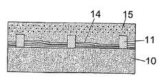
- a layer of oxide is grown on a Si substrate 10 and is then selectively etched after the area to be etched has been defined, for example by the application of a photoresist layer to the oxide layer and the selective exposure and development of the photoresist layer to form a photoresist mask. After etching elongate walls 11 of oxide extend substantially parallel to one another along the length of the substrate 10 and are separated by long thin strips 12 , as shown at a in FIG. 2 , within which a SiGe layer may subsequently be grown in the manner already described above.
- a SiGe layer 13 is selectively grown on each long thin strip 12 between the oxide walls 11 , as shown at b in FIG. 2 , at a temperature in the range from room temperature to 1200° C., and preferably in the range from 350 to 900° C.
- Such SiGe growth is selective such that there is substantially no growth of SiGe along the top of the oxide walls 11 .
- Such selective growth may be effected by chemical vapour deposition (CVD).
- dislocations 14 are caused to be generated at each oxide wall 11 and to extend along the shortest dimension towards the opposite oxide wall 11 .
- the SiGe material is caused to relax in the direction of the dislocations 14 which extend over the entire width of the area between the walls 11 .
- SiGe material is continued at a temperature in the range from room temperature to 1200° C., and preferably in the range from 350 to 900° C., to form a further SiGe layer 13 a continuous with the first SiGe layer 13 until lateral overgrowth of the SiGe material onto the top of the oxide walls 11 occurs, as shown at d in FIG. 2 .
- the grown areas of SiGe seeded in the areas between the oxide walls 11 will coalesce with each other and cover the entire surface of the Si substrate.
- the SiGe material grown in this manner may form a single crystalline layer, or alternatively there may be stacking faults where the different growth zones coalesce. It is in any case likely that the surface will be uneven where the different growth zones meet.
- the strain in the unrelieved longitudinal direction is eventually relaxed by the formation of dislocations extending in the longitudinal direction which are able to be nucleated from anywhere on the wafer. Since such nucleation has a much higher activation energy than nucleation from the oxide walls on the sides of the growth zone, the formation of such longitudinal dislocations 15 occurs at a much later stage than the formation of the dislocations 14 within the windows defined by the oxide walls 11 .
- the two sets of dislocations 13 , 15 do not interact with one another and the dislocations may extend over the whole surface of the wafer. Furthermore, because there is no strain in the SiGe material in a direction orthogonal to the outside walls 11 , there will be no driving force tending to produce dislocations in this direction. Furthermore, since any dislocation interactions are kept to a minimum, there are substantially no threading dislocations produced which would otherwise terminate at the upper surface of the SiGe material resulting in roughness of the surface.
- the height of the oxide walls 11 may vary from 10 nm to 1,000 nm depending on the Ge composition of the SiGe material, although it would normally be expected to be in the range of 400 nm to 700 nm.
- the oxide windows may range in width from 100 nm to 100 ⁇ m in width, and most likely are from 5 ⁇ m to 20 ⁇ m in width.
- the width of the oxide walls 11 is preferably as small as possible to ensure full lateral overgrowth, and currently the width is likely to be in the range from 100 nm to 10 ⁇ m, and preferably about 1 ⁇ m.
- the Ge composition within the SiGe material may be substantially constant through the thickness of the layer, although it would also be possible for the Ge composition to be graded so that it increases from a first composition at a lower level in the layer to a second, higher composition at a higher level in the layer.
- an uneven surface 16 may be obtained, as shown at d in FIG. 2 , and the effect of this may be overcome by a chemo-mechanical polishing (CMP) step to planarise the surface before a final capping layer is grown to obtain the final arrangement shown at e in FIG. 2 .
- CMP chemo-mechanical polishing
- an annealing step is applied to ensure full relaxation. Such an annealing step may be effected at any stage in the SiGe growth process, although it is preferably effected after the selective SiGe growth between the oxide walls 11 and before the further growth leading to overgrowth of the oxide walls 11 .
- the SiGe growth occurs on top of closely spaced mesa pillars defining the growth zones.
- the isolation between the strips is provided by the trenches between the pillars, rather than by isolating oxide walls, and the epitaxial growth process may be molecular beam epitaxy (MBE) or CVD.
- the SiGe material may be grown between spaced parallel walls of Si nitride or some other isolating material.
- the virtual substrate may be epitaxially grown on a patterned silicon wafer or a wafer having a patterned oxide layer such that growth only occurs in selected areas.
- the fabrication technique may be used to produce a virtual substrate in only one or more selected areas of the chip (as may be required for system-on-a-chip integration) in which enhanced circuit functionality is required, for example.
- the method of the invention is capable of a wide range of applications, including the provision of a virtual substrate for the growth of strained or relaxed Si, Ge or SiGe layers for fabrication of devices such as bipolar junction transistors (BJT), field effect transistors (FET) and resonance tunnelling diodes (RTD), as well as III–V semiconductor layers for high speed digital interface to CMOS technologies and optoelectronic applications including light emitting diodes (LEDs) and semiconductor lasers.
- BJT bipolar junction transistors
- FET field effect transistors
- RTD resonance tunnelling diodes
- III–V semiconductor layers for high speed digital interface to CMOS technologies and optoelectronic applications including light emitting diodes (LEDs) and semiconductor lasers.
Landscapes
- Recrystallisation Techniques (AREA)
Abstract
Description
Claims (26)
Applications Claiming Priority (3)
| Application Number | Priority Date | Filing Date | Title |
|---|---|---|---|
| GBGB0220438.6A GB0220438D0 (en) | 2002-09-03 | 2002-09-03 | Formation of lattice-turning semiconductor substrates |
| GB0220438.6 | 2002-09-03 | ||
| PCT/GB2003/003514 WO2004023536A1 (en) | 2002-09-03 | 2003-08-12 | Formation of lattice-tuning semiconductor substrates |
Publications (2)
| Publication Number | Publication Date |
|---|---|
| US20050245055A1 US20050245055A1 (en) | 2005-11-03 |
| US7179727B2 true US7179727B2 (en) | 2007-02-20 |
Family
ID=9943412
Family Applications (1)
| Application Number | Title | Priority Date | Filing Date |
|---|---|---|---|
| US10/525,987 Expired - Fee Related US7179727B2 (en) | 2002-09-03 | 2003-08-12 | Formation of lattice-tuning semiconductor substrates |
Country Status (8)
| Country | Link |
|---|---|
| US (1) | US7179727B2 (en) |
| EP (1) | EP1540715A1 (en) |
| JP (1) | JP2005537672A (en) |
| KR (1) | KR20050038037A (en) |
| CN (1) | CN100364052C (en) |
| AU (1) | AU2003251376A1 (en) |
| GB (1) | GB0220438D0 (en) |
| WO (1) | WO2004023536A1 (en) |
Cited By (22)
| Publication number | Priority date | Publication date | Assignee | Title |
|---|---|---|---|---|
| US20070212879A1 (en) * | 2004-09-22 | 2007-09-13 | Grasby Timothy J | Formation of lattice-tuning semiconductor substrates |
| US20070235744A1 (en) * | 2006-03-28 | 2007-10-11 | Dean Tran | Eutectic bonding of ultrathin semiconductors |
| US20080093622A1 (en) * | 2006-10-19 | 2008-04-24 | Amberwave Systems Corporation | Light-Emitter-Based Devices with Lattice-Mismatched Semiconductor Structures |
| US20080257409A1 (en) * | 2007-04-09 | 2008-10-23 | Amberwave Systems Corporation | Photovoltaics on silicon |
| US20090065047A1 (en) * | 2007-09-07 | 2009-03-12 | Amberwave Systems Corporation | Multi-Junction Solar Cells |
| US20100072515A1 (en) * | 2008-09-19 | 2010-03-25 | Amberwave Systems Corporation | Fabrication and structures of crystalline material |
| US20100078680A1 (en) * | 2008-09-24 | 2010-04-01 | Amberwave Systems Corporation | Semiconductor sensor structures with reduced dislocation defect densities and related methods for the same |
| US20100176371A1 (en) * | 2009-01-09 | 2010-07-15 | Taiwan Semiconductor Manufacturing Company, Ltd. | Semiconductor Diodes Fabricated by Aspect Ratio Trapping with Coalesced Films |
| US20100176375A1 (en) * | 2009-01-09 | 2010-07-15 | Taiwan Semiconductor Manufacturing Company, Ltd. | Diode-Based Devices and Methods for Making the Same |
| US20100213511A1 (en) * | 2006-03-24 | 2010-08-26 | Taiwan Semiconductor Manufacturing Company, Ltd. | Lattice-Mismatched Semiconductor Structures and Related Methods for Device Fabrication |
| US20100252861A1 (en) * | 2009-04-02 | 2010-10-07 | Taiwan Semiconductor Manufacturing Company, Ltd. | Devices Formed from a Non-Polar Plane of a Crystalline Material and Method of Making the Same |
| US20110011438A1 (en) * | 2007-04-09 | 2011-01-20 | Taiwan Semiconductor Manufacturing Company, Ltd. | Nitride-Based Multi-Junction Solar Cell Modules and Methods for Making the Same |
| US20110086498A1 (en) * | 2006-09-27 | 2011-04-14 | Taiwan Semiconductor Manufacturing Company, Ltd. | Quantum Tunneling Devices and Circuits with Lattice-Mismatched Semiconductor Structures |
| US8274097B2 (en) | 2008-07-01 | 2012-09-25 | Taiwan Semiconductor Manufacturing Company, Ltd. | Reduction of edge effects from aspect ratio trapping |
| US8324660B2 (en) | 2005-05-17 | 2012-12-04 | Taiwan Semiconductor Manufacturing Company, Ltd. | Lattice-mismatched semiconductor structures with reduced dislocation defect densities and related methods for device fabrication |
| US8329541B2 (en) | 2007-06-15 | 2012-12-11 | Taiwan Semiconductor Manufacturing Company, Ltd. | InP-based transistor fabrication |
| US8384196B2 (en) | 2008-09-19 | 2013-02-26 | Taiwan Semiconductor Manufacturing Company, Ltd. | Formation of devices by epitaxial layer overgrowth |
| US8822248B2 (en) | 2008-06-03 | 2014-09-02 | Taiwan Semiconductor Manufacturing Company, Ltd. | Epitaxial growth of crystalline material |
| US8847279B2 (en) | 2006-09-07 | 2014-09-30 | Taiwan Semiconductor Manufacturing Company, Ltd. | Defect reduction using aspect ratio trapping |
| US8890213B2 (en) | 2009-05-22 | 2014-11-18 | Sumitomo Chemical Company, Limited | Semiconductor wafer, electronic device, a method of producing semiconductor wafer, and method of producing electronic device |
| US8981427B2 (en) | 2008-07-15 | 2015-03-17 | Taiwan Semiconductor Manufacturing Company, Ltd. | Polishing of small composite semiconductor materials |
| US9859381B2 (en) | 2005-05-17 | 2018-01-02 | Taiwan Semiconductor Manufacturing Company, Ltd. | Lattice-mismatched semiconductor structures with reduced dislocation defect densities and related methods for device fabrication |
Families Citing this family (6)
| Publication number | Priority date | Publication date | Assignee | Title |
|---|---|---|---|---|
| WO2006011107A1 (en) * | 2004-07-22 | 2006-02-02 | Koninklijke Philips Electronics N.V. | Method of manufacturing a semiconductor device and semiconductor device obtained with such a method |
| CN101268547B (en) | 2005-07-26 | 2014-07-09 | 琥珀波系统公司 | Structures comprising alternating active region materials and methods of forming the same |
| US7638842B2 (en) | 2005-09-07 | 2009-12-29 | Amberwave Systems Corporation | Lattice-mismatched semiconductor structures on insulators |
| CN103367115A (en) * | 2007-12-28 | 2013-10-23 | 住友化学株式会社 | Semiconductor substrate, method for manufacturing semiconductor substrate, and electronic device |
| KR20110081804A (en) * | 2008-10-02 | 2011-07-14 | 스미또모 가가꾸 가부시키가이샤 | Substrate for semiconductor device, semiconductor device device, design system, manufacturing method and design method |
| JP6706414B2 (en) * | 2015-11-27 | 2020-06-10 | 国立研究開発法人情報通信研究機構 | Ge single crystal thin film manufacturing method and optical device |
Citations (12)
| Publication number | Priority date | Publication date | Assignee | Title |
|---|---|---|---|---|
| GB2215514A (en) | 1988-03-04 | 1989-09-20 | Plessey Co Plc | Terminating dislocations in semiconductor epitaxial layers |
| US5108947A (en) | 1989-01-31 | 1992-04-28 | Agfa-Gevaert N.V. | Integration of gaas on si substrates |
| US5158907A (en) * | 1990-08-02 | 1992-10-27 | At&T Bell Laboratories | Method for making semiconductor devices with low dislocation defects |
| US5238869A (en) | 1988-07-25 | 1993-08-24 | Texas Instruments Incorporated | Method of forming an epitaxial layer on a heterointerface |
| US5272105A (en) | 1988-02-11 | 1993-12-21 | Gte Laboratories Incorporated | Method of manufacturing an heteroepitaxial semiconductor structure |
| US5410167A (en) | 1992-07-10 | 1995-04-25 | Fujitsu Limited | Semiconductor device with reduced side gate effect |
| US5442205A (en) * | 1991-04-24 | 1995-08-15 | At&T Corp. | Semiconductor heterostructure devices with strained semiconductor layers |
| WO1999014804A1 (en) | 1997-09-16 | 1999-03-25 | Massachusetts Institute Of Technology | CO-PLANAR Si AND Ge COMPOSITE SUBSTRATE AND METHOD OF PRODUCING SAME |
| WO1999038201A1 (en) | 1998-01-27 | 1999-07-29 | Forschungszentrum Jülich GmbH | Method for the production of a monocrystalline layer on a substrate with a non-adapted lattice and component containing one or several such layers |
| EP1052684A1 (en) | 1999-05-10 | 2000-11-15 | Toyoda Gosei Co., Ltd. | A method for manufacturing group III nitride compound semiconductor and a light-emitting device using group III nitride compound semiconductor |
| WO2001001465A1 (en) | 1999-06-25 | 2001-01-04 | Massachusetts Institute Of Technology | Cyclic thermal anneal for dislocation reduction |
| US20020017642A1 (en) | 2000-08-01 | 2002-02-14 | Mitsubishi Materials Corporation | Semiconductor substrate, field effect transistor, method of forming SiGe layer and method of forming strained Si layer using same, and method of manufacturing field effect transistor |
Family Cites Families (6)
| Publication number | Priority date | Publication date | Assignee | Title |
|---|---|---|---|---|
| JPH04315419A (en) * | 1991-04-12 | 1992-11-06 | Nec Corp | Insulating film/compound semiconductor lamination structure on element semiconductor substrate |
| JPH06260427A (en) * | 1993-03-05 | 1994-09-16 | Nec Corp | Selective growth method of semiconductor film |
| US6039803A (en) * | 1996-06-28 | 2000-03-21 | Massachusetts Institute Of Technology | Utilization of miscut substrates to improve relaxed graded silicon-germanium and germanium layers on silicon |
| JP4406995B2 (en) * | 2000-03-27 | 2010-02-03 | パナソニック株式会社 | Semiconductor substrate and method for manufacturing semiconductor substrate |
| JP4345244B2 (en) * | 2001-05-31 | 2009-10-14 | 株式会社Sumco | Method of forming SiGe layer, method of forming strained Si layer using the same, and method of manufacturing field effect transistor |
| JP2004055943A (en) * | 2002-07-23 | 2004-02-19 | Matsushita Electric Ind Co Ltd | Semiconductor device and manufacturing method thereof |
-
2002
- 2002-09-03 GB GBGB0220438.6A patent/GB0220438D0/en not_active Ceased
-
2003
- 2003-08-12 US US10/525,987 patent/US7179727B2/en not_active Expired - Fee Related
- 2003-08-12 KR KR1020057003640A patent/KR20050038037A/en not_active Ceased
- 2003-08-12 WO PCT/GB2003/003514 patent/WO2004023536A1/en not_active Ceased
- 2003-08-12 JP JP2004533596A patent/JP2005537672A/en active Pending
- 2003-08-12 EP EP03793846A patent/EP1540715A1/en not_active Withdrawn
- 2003-08-12 CN CNB038209543A patent/CN100364052C/en not_active Expired - Fee Related
- 2003-08-12 AU AU2003251376A patent/AU2003251376A1/en not_active Abandoned
Patent Citations (12)
| Publication number | Priority date | Publication date | Assignee | Title |
|---|---|---|---|---|
| US5272105A (en) | 1988-02-11 | 1993-12-21 | Gte Laboratories Incorporated | Method of manufacturing an heteroepitaxial semiconductor structure |
| GB2215514A (en) | 1988-03-04 | 1989-09-20 | Plessey Co Plc | Terminating dislocations in semiconductor epitaxial layers |
| US5238869A (en) | 1988-07-25 | 1993-08-24 | Texas Instruments Incorporated | Method of forming an epitaxial layer on a heterointerface |
| US5108947A (en) | 1989-01-31 | 1992-04-28 | Agfa-Gevaert N.V. | Integration of gaas on si substrates |
| US5158907A (en) * | 1990-08-02 | 1992-10-27 | At&T Bell Laboratories | Method for making semiconductor devices with low dislocation defects |
| US5442205A (en) * | 1991-04-24 | 1995-08-15 | At&T Corp. | Semiconductor heterostructure devices with strained semiconductor layers |
| US5410167A (en) | 1992-07-10 | 1995-04-25 | Fujitsu Limited | Semiconductor device with reduced side gate effect |
| WO1999014804A1 (en) | 1997-09-16 | 1999-03-25 | Massachusetts Institute Of Technology | CO-PLANAR Si AND Ge COMPOSITE SUBSTRATE AND METHOD OF PRODUCING SAME |
| WO1999038201A1 (en) | 1998-01-27 | 1999-07-29 | Forschungszentrum Jülich GmbH | Method for the production of a monocrystalline layer on a substrate with a non-adapted lattice and component containing one or several such layers |
| EP1052684A1 (en) | 1999-05-10 | 2000-11-15 | Toyoda Gosei Co., Ltd. | A method for manufacturing group III nitride compound semiconductor and a light-emitting device using group III nitride compound semiconductor |
| WO2001001465A1 (en) | 1999-06-25 | 2001-01-04 | Massachusetts Institute Of Technology | Cyclic thermal anneal for dislocation reduction |
| US20020017642A1 (en) | 2000-08-01 | 2002-02-14 | Mitsubishi Materials Corporation | Semiconductor substrate, field effect transistor, method of forming SiGe layer and method of forming strained Si layer using same, and method of manufacturing field effect transistor |
Non-Patent Citations (1)
| Title |
|---|
| "Molecular beam epitaxy of strained Si<SUB>1-x</SUB>Ge<SUB>x </SUB>layers on patterned substrates" Jun. 1, 1993, Journal of Crystal Growth, North-Holland Publishing Co., vol. 130, Nos. 3/4, pp. 611-616, Bugiel et al. |
Cited By (75)
| Publication number | Priority date | Publication date | Assignee | Title |
|---|---|---|---|---|
| US20070212879A1 (en) * | 2004-09-22 | 2007-09-13 | Grasby Timothy J | Formation of lattice-tuning semiconductor substrates |
| US8796734B2 (en) | 2005-05-17 | 2014-08-05 | Taiwan Semiconductor Manufacturing Company, Ltd. | Lattice-mismatched semiconductor structures with reduced dislocation defect densities and related methods for device fabrication |
| US8519436B2 (en) | 2005-05-17 | 2013-08-27 | Taiwan Semiconductor Manufacturing Company, Ltd. | Lattice-mismatched semiconductor structures with reduced dislocation defect densities and related methods for device fabrication |
| US11251272B2 (en) | 2005-05-17 | 2022-02-15 | Taiwan Semiconductor Manufacturing Company, Ltd. | Lattice-mismatched semiconductor structures with reduced dislocation defect densities and related methods for device fabrication |
| US8629477B2 (en) | 2005-05-17 | 2014-01-14 | Taiwan Semiconductor Manufacturing Company, Ltd. | Lattice-mismatched semiconductor structures with reduced dislocation defect densities and related methods for device fabrication |
| US10522629B2 (en) | 2005-05-17 | 2019-12-31 | Taiwan Semiconductor Manufacturing Company, Ltd. | Lattice-mismatched semiconductor structures with reduced dislocation defect densities and related methods for device fabrication |
| US8987028B2 (en) | 2005-05-17 | 2015-03-24 | Taiwan Semiconductor Manufacturing Company, Ltd. | Lattice-mismatched semiconductor structures with reduced dislocation defect densities and related methods for device fabrication |
| US8324660B2 (en) | 2005-05-17 | 2012-12-04 | Taiwan Semiconductor Manufacturing Company, Ltd. | Lattice-mismatched semiconductor structures with reduced dislocation defect densities and related methods for device fabrication |
| US9859381B2 (en) | 2005-05-17 | 2018-01-02 | Taiwan Semiconductor Manufacturing Company, Ltd. | Lattice-mismatched semiconductor structures with reduced dislocation defect densities and related methods for device fabrication |
| US9219112B2 (en) | 2005-05-17 | 2015-12-22 | Taiwan Semiconductor Manufacturing Company, Ltd. | Lattice-mismatched semiconductor structures with reduced dislocation defect densities and related methods for device fabrication |
| US9431243B2 (en) | 2005-05-17 | 2016-08-30 | Taiwan Semiconductor Manufacturing Company, Ltd. | Lattice-mismatched semiconductor structures with reduced dislocation defect densities and related methods for device fabrication |
| US8878243B2 (en) | 2006-03-24 | 2014-11-04 | Taiwan Semiconductor Manufacturing Company, Ltd. | Lattice-mismatched semiconductor structures and related methods for device fabrication |
| US20100213511A1 (en) * | 2006-03-24 | 2010-08-26 | Taiwan Semiconductor Manufacturing Company, Ltd. | Lattice-Mismatched Semiconductor Structures and Related Methods for Device Fabrication |
| US10074536B2 (en) | 2006-03-24 | 2018-09-11 | Taiwan Semiconductor Manufacturing Company, Ltd. | Lattice-mismatched semiconductor structures and related methods for device fabrication |
| US7476606B2 (en) * | 2006-03-28 | 2009-01-13 | Northrop Grumman Corporation | Eutectic bonding of ultrathin semiconductors |
| US20070235744A1 (en) * | 2006-03-28 | 2007-10-11 | Dean Tran | Eutectic bonding of ultrathin semiconductors |
| US9318325B2 (en) | 2006-09-07 | 2016-04-19 | Taiwan Semiconductor Manufacturing Company, Ltd. | Defect reduction using aspect ratio trapping |
| US9818819B2 (en) | 2006-09-07 | 2017-11-14 | Taiwan Semiconductor Manufacturing Company, Ltd. | Defect reduction using aspect ratio trapping |
| US8847279B2 (en) | 2006-09-07 | 2014-09-30 | Taiwan Semiconductor Manufacturing Company, Ltd. | Defect reduction using aspect ratio trapping |
| US8216951B2 (en) | 2006-09-27 | 2012-07-10 | Taiwan Semiconductor Manufacturing Company, Ltd. | Quantum tunneling devices and circuits with lattice-mismatched semiconductor structures |
| US9105522B2 (en) | 2006-09-27 | 2015-08-11 | Taiwan Semiconductor Manufacturing Company, Ltd. | Quantum tunneling devices and circuits with lattice-mismatched semiconductor structures |
| US20110086498A1 (en) * | 2006-09-27 | 2011-04-14 | Taiwan Semiconductor Manufacturing Company, Ltd. | Quantum Tunneling Devices and Circuits with Lattice-Mismatched Semiconductor Structures |
| US9559712B2 (en) | 2006-09-27 | 2017-01-31 | Taiwan Semiconductor Manufacturing Company, Ltd. | Quantum tunneling devices and circuits with lattice-mismatched semiconductor structures |
| US8860160B2 (en) | 2006-09-27 | 2014-10-14 | Taiwan Semiconductor Manufacturing Company, Ltd. | Quantum tunneling devices and circuits with lattice-mismatched semiconductor structures |
| US8629047B2 (en) | 2006-09-27 | 2014-01-14 | Taiwan Semiconductor Manufacturing Company, Ltd. | Quantum tunneling devices and circuits with lattice-mismatched semiconductor structures |
| US10468551B2 (en) | 2006-10-19 | 2019-11-05 | Taiwan Semiconductor Manufacturing Company, Ltd. | Light-emitter-based devices with lattice-mismatched semiconductor structures |
| US20080093622A1 (en) * | 2006-10-19 | 2008-04-24 | Amberwave Systems Corporation | Light-Emitter-Based Devices with Lattice-Mismatched Semiconductor Structures |
| US8502263B2 (en) | 2006-10-19 | 2013-08-06 | Taiwan Semiconductor Manufacturing Company, Ltd. | Light-emitter-based devices with lattice-mismatched semiconductor structures |
| US9508890B2 (en) | 2007-04-09 | 2016-11-29 | Taiwan Semiconductor Manufacturing Company, Ltd. | Photovoltaics on silicon |
| US20080257409A1 (en) * | 2007-04-09 | 2008-10-23 | Amberwave Systems Corporation | Photovoltaics on silicon |
| US9231073B2 (en) | 2007-04-09 | 2016-01-05 | Taiwan Semiconductor Manufacturing Company, Ltd. | Diode-based devices and methods for making the same |
| US10680126B2 (en) | 2007-04-09 | 2020-06-09 | Taiwan Semiconductor Manufacturing Company, Ltd. | Photovoltaics on silicon |
| US9449868B2 (en) | 2007-04-09 | 2016-09-20 | Taiwan Semiconductor Manufacutring Company, Ltd. | Methods of forming semiconductor diodes by aspect ratio trapping with coalesced films |
| US8624103B2 (en) | 2007-04-09 | 2014-01-07 | Taiwan Semiconductor Manufacturing Company, Ltd. | Nitride-based multi-junction solar cell modules and methods for making the same |
| US20110011438A1 (en) * | 2007-04-09 | 2011-01-20 | Taiwan Semiconductor Manufacturing Company, Ltd. | Nitride-Based Multi-Junction Solar Cell Modules and Methods for Making the Same |
| US9543472B2 (en) | 2007-04-09 | 2017-01-10 | Taiwan Semiconductor Manufacturing Company, Ltd. | Diode-based devices and methods for making the same |
| US9040331B2 (en) | 2007-04-09 | 2015-05-26 | Taiwan Semiconductor Manufacturing Company, Ltd. | Diode-based devices and methods for making the same |
| US9853176B2 (en) | 2007-04-09 | 2017-12-26 | Taiwan Semiconductor Manufacturing Company, Ltd. | Nitride-based multi-junction solar cell modules and methods for making the same |
| US9853118B2 (en) | 2007-04-09 | 2017-12-26 | Taiwan Semiconductor Manufacturing Company, Ltd. | Diode-based devices and methods for making the same |
| US9780190B2 (en) | 2007-06-15 | 2017-10-03 | Taiwan Semiconductor Manufacturing Company, Ltd. | InP-based transistor fabrication |
| US8329541B2 (en) | 2007-06-15 | 2012-12-11 | Taiwan Semiconductor Manufacturing Company, Ltd. | InP-based transistor fabrication |
| US10002981B2 (en) | 2007-09-07 | 2018-06-19 | Taiwan Semiconductor Manufacturing Company, Ltd. | Multi-junction solar cells |
| US8344242B2 (en) | 2007-09-07 | 2013-01-01 | Taiwan Semiconductor Manufacturing Company, Ltd. | Multi-junction solar cells |
| US20090065047A1 (en) * | 2007-09-07 | 2009-03-12 | Amberwave Systems Corporation | Multi-Junction Solar Cells |
| US9365949B2 (en) | 2008-06-03 | 2016-06-14 | Taiwan Semiconductor Manufacturing Company, Ltd. | Epitaxial growth of crystalline material |
| US8822248B2 (en) | 2008-06-03 | 2014-09-02 | Taiwan Semiconductor Manufacturing Company, Ltd. | Epitaxial growth of crystalline material |
| US10961639B2 (en) | 2008-06-03 | 2021-03-30 | Taiwan Semiconductor Manufacturing Company, Ltd. | Epitaxial growth of crystalline material |
| US8994070B2 (en) | 2008-07-01 | 2015-03-31 | Taiwan Semiconductor Manufacturing Company, Ltd. | Reduction of edge effects from aspect ratio trapping |
| US9356103B2 (en) | 2008-07-01 | 2016-05-31 | Taiwan Semiconductor Manufacturing Company, Ltd. | Reduction of edge effects from aspect ratio trapping |
| US8629045B2 (en) | 2008-07-01 | 2014-01-14 | Taiwan Semiconductor Manufacturing Company, Ltd. | Reduction of edge effects from aspect ratio trapping |
| US8274097B2 (en) | 2008-07-01 | 2012-09-25 | Taiwan Semiconductor Manufacturing Company, Ltd. | Reduction of edge effects from aspect ratio trapping |
| US9640395B2 (en) | 2008-07-01 | 2017-05-02 | Taiwan Semiconductor Manufacturing Company, Ltd. | Reduction of edge effects from aspect ratio trapping |
| US9607846B2 (en) | 2008-07-15 | 2017-03-28 | Taiwan Semiconductor Manufacturing Company, Ltd. | Polishing of small composite semiconductor materials |
| US8981427B2 (en) | 2008-07-15 | 2015-03-17 | Taiwan Semiconductor Manufacturing Company, Ltd. | Polishing of small composite semiconductor materials |
| US9287128B2 (en) | 2008-07-15 | 2016-03-15 | Taiwan Semiconductor Manufacturing Company, Ltd. | Polishing of small composite semiconductor materials |
| US9934967B2 (en) | 2008-09-19 | 2018-04-03 | Taiwan Semiconductor Manufacturing Co., Ltd. | Formation of devices by epitaxial layer overgrowth |
| US9984872B2 (en) | 2008-09-19 | 2018-05-29 | Taiwan Semiconductor Manufacturing Company, Ltd. | Fabrication and structures of crystalline material |
| US8384196B2 (en) | 2008-09-19 | 2013-02-26 | Taiwan Semiconductor Manufacturing Company, Ltd. | Formation of devices by epitaxial layer overgrowth |
| US20100072515A1 (en) * | 2008-09-19 | 2010-03-25 | Amberwave Systems Corporation | Fabrication and structures of crystalline material |
| US8253211B2 (en) | 2008-09-24 | 2012-08-28 | Taiwan Semiconductor Manufacturing Company, Ltd. | Semiconductor sensor structures with reduced dislocation defect densities |
| US9105549B2 (en) | 2008-09-24 | 2015-08-11 | Taiwan Semiconductor Manufacturing Company, Ltd. | Semiconductor sensor structures with reduced dislocation defect densities |
| US8809106B2 (en) | 2008-09-24 | 2014-08-19 | Taiwan Semiconductor Manufacturing Company, Ltd. | Method for semiconductor sensor structures with reduced dislocation defect densities |
| US20100078680A1 (en) * | 2008-09-24 | 2010-04-01 | Amberwave Systems Corporation | Semiconductor sensor structures with reduced dislocation defect densities and related methods for the same |
| US9455299B2 (en) | 2008-09-24 | 2016-09-27 | Taiwan Semiconductor Manufacturing Company, Ltd. | Methods for semiconductor sensor structures with reduced dislocation defect densities |
| US8237151B2 (en) | 2009-01-09 | 2012-08-07 | Taiwan Semiconductor Manufacturing Company, Ltd. | Diode-based devices and methods for making the same |
| US20100176371A1 (en) * | 2009-01-09 | 2010-07-15 | Taiwan Semiconductor Manufacturing Company, Ltd. | Semiconductor Diodes Fabricated by Aspect Ratio Trapping with Coalesced Films |
| US8304805B2 (en) | 2009-01-09 | 2012-11-06 | Taiwan Semiconductor Manufacturing Company, Ltd. | Semiconductor diodes fabricated by aspect ratio trapping with coalesced films |
| US20100176375A1 (en) * | 2009-01-09 | 2010-07-15 | Taiwan Semiconductor Manufacturing Company, Ltd. | Diode-Based Devices and Methods for Making the Same |
| US9029908B2 (en) | 2009-01-09 | 2015-05-12 | Taiwan Semiconductor Manufacturing Company, Ltd. | Semiconductor diodes fabricated by aspect ratio trapping with coalesced films |
| US8765510B2 (en) | 2009-01-09 | 2014-07-01 | Taiwan Semiconductor Manufacturing Company, Ltd. | Semiconductor diodes fabricated by aspect ratio trapping with coalesced films |
| US9299562B2 (en) | 2009-04-02 | 2016-03-29 | Taiwan Semiconductor Manufacturing Company, Ltd. | Devices formed from a non-polar plane of a crystalline material and method of making the same |
| US9576951B2 (en) | 2009-04-02 | 2017-02-21 | Taiwan Semiconductor Manufacturing Company, Ltd. | Devices formed from a non-polar plane of a crystalline material and method of making the same |
| US20100252861A1 (en) * | 2009-04-02 | 2010-10-07 | Taiwan Semiconductor Manufacturing Company, Ltd. | Devices Formed from a Non-Polar Plane of a Crystalline Material and Method of Making the Same |
| US8629446B2 (en) | 2009-04-02 | 2014-01-14 | Taiwan Semiconductor Manufacturing Company, Ltd. | Devices formed from a non-polar plane of a crystalline material and method of making the same |
| US8890213B2 (en) | 2009-05-22 | 2014-11-18 | Sumitomo Chemical Company, Limited | Semiconductor wafer, electronic device, a method of producing semiconductor wafer, and method of producing electronic device |
Also Published As
| Publication number | Publication date |
|---|---|
| CN100364052C (en) | 2008-01-23 |
| WO2004023536A1 (en) | 2004-03-18 |
| JP2005537672A (en) | 2005-12-08 |
| CN1714427A (en) | 2005-12-28 |
| KR20050038037A (en) | 2005-04-25 |
| US20050245055A1 (en) | 2005-11-03 |
| AU2003251376A1 (en) | 2004-03-29 |
| EP1540715A1 (en) | 2005-06-15 |
| GB0220438D0 (en) | 2002-10-09 |
Similar Documents
| Publication | Publication Date | Title |
|---|---|---|
| US7179727B2 (en) | Formation of lattice-tuning semiconductor substrates | |
| EP1687841B1 (en) | Formation of lattice-tuning semiconductor substrates | |
| US7214598B2 (en) | Formation of lattice-tuning semiconductor substrates | |
| KR101225816B1 (en) | Lattice-mismatched semiconductor structures with reduced dislocation defect densities and related methods for device fabrication | |
| US6039803A (en) | Utilization of miscut substrates to improve relaxed graded silicon-germanium and germanium layers on silicon | |
| KR100650454B1 (en) | SEMICONDUCTOR SUBSTRATE, FIELD EFFECT TRANSISTOR, METHOD OF FORMING SiGe LAYER, METHOD OF FORMING STRAINED Si LAYER USING THE SAME, AND METHOD OF MANUFACTURING FIELD EFFECT TRANSISTOR | |
| US8823056B2 (en) | Semiconductor heterostructures having reduced dislocation pile-ups and related methods | |
| US9773906B2 (en) | Relaxed semiconductor layers with reduced defects and methods of forming the same | |
| US20060131606A1 (en) | Lattice-mismatched semiconductor structures employing seed layers and related fabrication methods | |
| US20130285116A1 (en) | Lattice-Mismatched Semiconductor Structures with Reduced Dislocation Defect Densities and Related Methods for Device Fabrication | |
| WO1998000857A9 (en) | Utilization of miscut substrates to improve relaxed graded silicon-germanium and germanium layers on silicon | |
| JP2005510081A (en) | Fabrication method of high mobility silicon germanium structure by low energy plasma enhanced chemical vapor deposition | |
| KR100531177B1 (en) | Method of fabricating strained thin film semiconductor layer | |
| KR20190122816A (en) | Group III-nitride structures with successively reduced crystallographic dislocation density regions | |
| US20070212879A1 (en) | Formation of lattice-tuning semiconductor substrates | |
| KR20220160890A (en) | Ⅲ-N semiconductor structure and method of manufacturing the same | |
| KR20130007546A (en) | Semiconductor substrate, semiconductor device, and method for manufacturing semiconductor substrate | |
| JPH05267175A (en) | Compound semiconductor substrate | |
| KR19980045996A (en) | Quantum thin wire structure of multilayer compound semiconductor and its formation method | |
| JPH0722317A (en) | Compound semiconductor substrate | |
| JPH03197393A (en) | Epitaxial growth of iii-v compound semiconductor on silicon substrate |
Legal Events
| Date | Code | Title | Description |
|---|---|---|---|
| AS | Assignment |
Owner name: WARWICK, UNIVERSITY OF, UNITED KINGDOM Free format text: ASSIGNMENT OF ASSIGNORS INTEREST;ASSIGNORS:CAPEWELL, ADAM DANIEL;GRASBY, TIMOTHY JOHN;PARKER, EVAN HUBERT CRESSWELL;AND OTHERS;REEL/FRAME:016807/0911 Effective date: 20050124 |
|
| AS | Assignment |
Owner name: ADVANCESIS LIMITED, UNITED KINGDOM Free format text: ASSIGNMENT OF ASSIGNORS INTEREST;ASSIGNOR:WARWICK, THE UNIVERSITY OF;REEL/FRAME:018270/0600 Effective date: 20060821 Owner name: ADVANCESIS LIMITED, UNITED KINGDOM Free format text: ASSIGNMENT OF ASSIGNORS INTEREST;ASSIGNOR:WARWICK, THE UNIVERITY OF;REEL/FRAME:018270/0641 Effective date: 20060821 |
|
| FEPP | Fee payment procedure |
Free format text: PAYOR NUMBER ASSIGNED (ORIGINAL EVENT CODE: ASPN); ENTITY STATUS OF PATENT OWNER: LARGE ENTITY |
|
| FPAY | Fee payment |
Year of fee payment: 4 |
|
| REMI | Maintenance fee reminder mailed | ||
| LAPS | Lapse for failure to pay maintenance fees | ||
| STCH | Information on status: patent discontinuation |
Free format text: PATENT EXPIRED DUE TO NONPAYMENT OF MAINTENANCE FEES UNDER 37 CFR 1.362 |
|
| STCH | Information on status: patent discontinuation |
Free format text: PATENT EXPIRED DUE TO NONPAYMENT OF MAINTENANCE FEES UNDER 37 CFR 1.362 |
|
| FP | Lapsed due to failure to pay maintenance fee |
Effective date: 20150220 |