JP2005537672A - Formation of lattice-adjusted semiconductor substrate - Google Patents
Formation of lattice-adjusted semiconductor substrate Download PDFInfo
- Publication number
- JP2005537672A JP2005537672A JP2004533596A JP2004533596A JP2005537672A JP 2005537672 A JP2005537672 A JP 2005537672A JP 2004533596 A JP2004533596 A JP 2004533596A JP 2004533596 A JP2004533596 A JP 2004533596A JP 2005537672 A JP2005537672 A JP 2005537672A
- Authority
- JP
- Japan
- Prior art keywords
- sige layer
- sige
- layer
- dislocations
- insulating means
- Prior art date
- Legal status (The legal status is an assumption and is not a legal conclusion. Google has not performed a legal analysis and makes no representation as to the accuracy of the status listed.)
- Pending
Links
Images

Classifications
-
- H—ELECTRICITY
- H01—ELECTRIC ELEMENTS
- H01L—SEMICONDUCTOR DEVICES NOT COVERED BY CLASS H10
- H01L21/00—Processes or apparatus adapted for the manufacture or treatment of semiconductor or solid state devices or of parts thereof
- H01L21/02—Manufacture or treatment of semiconductor devices or of parts thereof
- H01L21/04—Manufacture or treatment of semiconductor devices or of parts thereof the devices having at least one potential-jump barrier or surface barrier, e.g. PN junction, depletion layer or carrier concentration layer
- H01L21/18—Manufacture or treatment of semiconductor devices or of parts thereof the devices having at least one potential-jump barrier or surface barrier, e.g. PN junction, depletion layer or carrier concentration layer the devices having semiconductor bodies comprising elements of Group IV of the Periodic System or AIIIBV compounds with or without impurities, e.g. doping materials
- H01L21/20—Deposition of semiconductor materials on a substrate, e.g. epitaxial growth solid phase epitaxy
-
- H—ELECTRICITY
- H01—ELECTRIC ELEMENTS
- H01L—SEMICONDUCTOR DEVICES NOT COVERED BY CLASS H10
- H01L21/00—Processes or apparatus adapted for the manufacture or treatment of semiconductor or solid state devices or of parts thereof
- H01L21/02—Manufacture or treatment of semiconductor devices or of parts thereof
- H01L21/02104—Forming layers
- H01L21/02365—Forming inorganic semiconducting materials on a substrate
- H01L21/02612—Formation types
- H01L21/02617—Deposition types
- H01L21/02636—Selective deposition, e.g. simultaneous growth of mono- and non-monocrystalline semiconductor materials
- H01L21/02647—Lateral overgrowth
-
- H—ELECTRICITY
- H01—ELECTRIC ELEMENTS
- H01L—SEMICONDUCTOR DEVICES NOT COVERED BY CLASS H10
- H01L21/00—Processes or apparatus adapted for the manufacture or treatment of semiconductor or solid state devices or of parts thereof
- H01L21/02—Manufacture or treatment of semiconductor devices or of parts thereof
- H01L21/02104—Forming layers
- H01L21/02365—Forming inorganic semiconducting materials on a substrate
- H01L21/02367—Substrates
- H01L21/0237—Materials
- H01L21/02373—Group 14 semiconducting materials
- H01L21/02381—Silicon, silicon germanium, germanium
-
- H—ELECTRICITY
- H01—ELECTRIC ELEMENTS
- H01L—SEMICONDUCTOR DEVICES NOT COVERED BY CLASS H10
- H01L21/00—Processes or apparatus adapted for the manufacture or treatment of semiconductor or solid state devices or of parts thereof
- H01L21/02—Manufacture or treatment of semiconductor devices or of parts thereof
- H01L21/02104—Forming layers
- H01L21/02365—Forming inorganic semiconducting materials on a substrate
- H01L21/02436—Intermediate layers between substrates and deposited layers
- H01L21/02439—Materials
- H01L21/02441—Group 14 semiconducting materials
- H01L21/0245—Silicon, silicon germanium, germanium
-
- H—ELECTRICITY
- H01—ELECTRIC ELEMENTS
- H01L—SEMICONDUCTOR DEVICES NOT COVERED BY CLASS H10
- H01L21/00—Processes or apparatus adapted for the manufacture or treatment of semiconductor or solid state devices or of parts thereof
- H01L21/02—Manufacture or treatment of semiconductor devices or of parts thereof
- H01L21/02104—Forming layers
- H01L21/02365—Forming inorganic semiconducting materials on a substrate
- H01L21/02518—Deposited layers
- H01L21/02521—Materials
- H01L21/02524—Group 14 semiconducting materials
- H01L21/02532—Silicon, silicon germanium, germanium
-
- H—ELECTRICITY
- H01—ELECTRIC ELEMENTS
- H01L—SEMICONDUCTOR DEVICES NOT COVERED BY CLASS H10
- H01L21/00—Processes or apparatus adapted for the manufacture or treatment of semiconductor or solid state devices or of parts thereof
- H01L21/02—Manufacture or treatment of semiconductor devices or of parts thereof
- H01L21/02104—Forming layers
- H01L21/02365—Forming inorganic semiconducting materials on a substrate
- H01L21/02612—Formation types
- H01L21/02617—Deposition types
- H01L21/02636—Selective deposition, e.g. simultaneous growth of mono- and non-monocrystalline semiconductor materials
- H01L21/02639—Preparation of substrate for selective deposition
-
- Y—GENERAL TAGGING OF NEW TECHNOLOGICAL DEVELOPMENTS; GENERAL TAGGING OF CROSS-SECTIONAL TECHNOLOGIES SPANNING OVER SEVERAL SECTIONS OF THE IPC; TECHNICAL SUBJECTS COVERED BY FORMER USPC CROSS-REFERENCE ART COLLECTIONS [XRACs] AND DIGESTS
- Y10—TECHNICAL SUBJECTS COVERED BY FORMER USPC
- Y10S—TECHNICAL SUBJECTS COVERED BY FORMER USPC CROSS-REFERENCE ART COLLECTIONS [XRACs] AND DIGESTS
- Y10S438/00—Semiconductor device manufacturing: process
- Y10S438/933—Germanium or silicon or Ge-Si on III-V
Abstract
格子調整半導体基板の形成方法であって、平行配置された酸化物壁(2)を表面の上に設けることによってSi表面から成る平行細片を画定する工程、第1SiGe層を細片の上に選択的に成長させて第1転位(3)が優先的に壁(2)の間の第1SiGe層を横切って延びて第1SiGe層の歪みを壁(2)に直交する方向に緩和する工程、及び第2SiGe層を第1SiGe層の上部の上に成長させて壁(2)を覆うように成長させ、第2転位が優先的に壁(2)上方の第2SiGe層の内部に形成されて、第2SiGe層の歪みを第1転位(3)と直交する方向に緩和する工程を含む。このようにして形成される転位は、材料を2つの互いに直交する方向に緩和するように形成されるが、他方では、これらの転位が空間的に分離されて2組の転位が互いに作用することができない。このように、貫通転位密度及び表面粗さの両方が大きく低減されるので、能動素子の電子散乱及び電子の移動速度の低下を招く原子格子の崩壊を減少させることにより仮想基板の性能が向上する。A method of forming a lattice-adjusted semiconductor substrate, wherein parallel strips of oxide surfaces (2) are provided on a surface to define parallel strips of a Si surface, a first SiGe layer on the strips Selectively growing and the first dislocations (3) preferentially extend across the first SiGe layer between the walls (2) to relieve strain in the first SiGe layer in a direction perpendicular to the walls (2); And a second SiGe layer is grown on top of the first SiGe layer to cover the wall (2), and second dislocations are preferentially formed inside the second SiGe layer above the wall (2); A step of relaxing strain of the second SiGe layer in a direction orthogonal to the first dislocation (3). The dislocations thus formed are formed so as to relax the material in two mutually orthogonal directions, but on the other hand, these dislocations are spatially separated and the two sets of dislocations interact with each other. I can't. Thus, both threading dislocation density and surface roughness are greatly reduced, thereby improving the performance of the virtual substrate by reducing atomic lattice collapse leading to reduced electron scattering and electron transfer speed of the active device. .
Description
本発明は格子調整半導体基板の形成に関し、これに限定されるものではないが、特に、内部にMOSFETのような能動半導体素子を形成することができる歪みシリコン(strained silicon)活性層又は歪みSiGe活性層及び歪のないIII−V族半導体活性層の成長に適する緩和SiGe(シリコン/ゲルマニウム)「仮想基板」の形成に関する。 The present invention relates to the formation of a lattice-adjusted semiconductor substrate, but is not limited to this. In particular, a strained silicon active layer or a strained SiGe active layer capable of forming an active semiconductor element such as a MOSFET therein. It relates to the formation of relaxed SiGe (silicon / germanium) “virtual substrates” suitable for the growth of layers and strain-free III-V semiconductor active layers.
歪みSi層をSiウェハの上に、緩和SiGeバッファ層を歪みSi層とSiウェハとの間に挟んで成長させ、MOSFETのような半導体素子を歪みSi層の内部に形成して半導体素子の特性を向上させる方法が知られている。下地Si基板の格子間隔よりも格子間隔を大きくするためにバッファ層を設けるので、バッファ層は一般的に仮想基板と呼ばれている。 A strained Si layer is grown on the Si wafer, a relaxed SiGe buffer layer is grown between the strained Si layer and the Si wafer, and a semiconductor element such as a MOSFET is formed inside the strained Si layer to provide characteristics of the semiconductor element. There are known methods for improving the above. Since a buffer layer is provided to make the lattice spacing larger than the lattice spacing of the underlying Si substrate, the buffer layer is generally called a virtual substrate.
シリコン及びゲルマニウムの合金(SiGe)をシリコン基板の上にエピタキシャル成長させてバッファ層を形成することが知られている。SiGeの格子間隔はSiの正常な格子間隔よりも大きいので、バッファ層が緩和してもよい場合にはこのようなバッファ層を設けることによって格子間隔を所望通りに大きくすることができる。 It is known to form a buffer layer by epitaxially growing an alloy of silicon and germanium (SiGe) on a silicon substrate. Since the lattice spacing of SiGe is larger than the normal lattice spacing of Si, when the buffer layer may be relaxed, the lattice spacing can be increased as desired by providing such a buffer layer.
バッファ層が緩和すると必然的にバッファ層に転位が形成されて歪みが緩和される。これらの転位によって普通歪み界面に伸びて長い転位を形成するハーフループが下地表面から形成される。しかしながら、バッファ層の深さを貫通する転位が形成されると基板の品質を劣化させてしまう。というのは、このような転位によって表面がでこぼこになり、能動半導体素子の内部で電子散乱が生じるからである。また、SiGe層の歪みを緩和するために多くの転位が必要となるので、このような転位が必然的に相互に作用し合い、貫通転位のピンニングを生じさせる。更に多くの転位が緩和を一層促進するために必要となると、その結果として貫通転位密度が高くなる。 When the buffer layer is relaxed, dislocations are inevitably formed in the buffer layer, and the strain is relaxed. These dislocations form a half loop from the underlying surface that extends to the normal strain interface and forms long dislocations. However, the formation of dislocations that penetrate the depth of the buffer layer degrades the quality of the substrate. This is because such dislocations cause the surface to be uneven and cause electron scattering inside the active semiconductor device. In addition, since many dislocations are required to relieve the strain of the SiGe layer, such dislocations necessarily interact with each other and cause pinning of threading dislocations. As more dislocations are needed to further promote relaxation, the threading dislocation density increases as a result.
米国特許第5442205号、米国特許第5221413号、国際公開番号WO98/00857、及び日本国特願平6−252046号に開示されているようなバッファ層を形成する公知の技術では、層のGe組成に直線的な傾斜を持たせて、歪み界面を傾斜領域全体に渡って分散させる。これは、それによって形成される転位も傾斜領域全体に渡って分散されるので、転位が相互に作用し難くなることを意味する。しかしながらこのような技術では、転位の主要発生源が増倍機構であり、この機構では、多くの転位が同じ発生源から生成されるので、転位が群となって通常同じ原子英進面の上に集まるという不具合が生じる。これらの転位群から生じる歪み領域は仮想基板表面に大きなうねりを生じ、これら歪み領域及び大きなうねりの両方は、仮想基板の品質に悪影響を及ぼし、且つ貫通転位を閉じ込めてしまうという影響を更にもたらす。 Known techniques for forming buffer layers such as those disclosed in US Pat. No. 5,442,205, US Pat. No. 5,212,413, International Publication No. WO 98/00857, and Japanese Patent Application No. 6-252046, the Ge composition of the layer Is provided with a linear inclination to disperse the strain interface over the entire inclined region. This means that the dislocations formed thereby are dispersed over the entire inclined region, so that the dislocations hardly interact with each other. However, in such a technique, the primary source of dislocations is the multiplication mechanism, and in this mechanism, many dislocations are generated from the same source, so the dislocations are grouped and usually on the same atomic plane. The problem of gathering in The strain regions resulting from these dislocation groups cause large undulations on the virtual substrate surface, and both these strain regions and large undulations adversely affect the quality of the virtual substrate and further have the effect of confining threading dislocations.
米国特許出願公開2002/0017642A1は、バッファ層を複数の積層膜から形成する技術について記載している。この技術では、複数の積層膜は、傾斜SiGe層、及び傾斜SiGe層の上の均一SiGe層を交互に重ねた層を含み、傾斜SiGe層は、傾斜SiGe層の下地となる材料のGe組成比からそれよりも大きな組成比にまで徐々に増加するGe組成比を有し、均一SiGe層は層の厚さ全体に渡ってほぼ一定の高い値のGe組成比を有する。このように、傾斜SiGe層及び均一SiGe層を交互に重ねて形成して、バッファ層全体に渡ってGe組成比に階段状の変化を持たせることにより、転位が界面で横方向に伝搬し易くなり、その結果、貫通転位が生じ難くなるので表面粗さが小さくなり易い。しかしながら、この技術において満足できる性能を得るためには、かなり厚く、細心の注意を払って傾斜を持たせた層を交互に設ける必要があり、しかも貫通転位が形成されることによって性能が劣化するという問題は依然として残る。 US 2002/0017642 A1 describes a technique for forming a buffer layer from a plurality of laminated films. In this technique, the plurality of stacked films include a graded SiGe layer and a layer in which uniform SiGe layers on the graded SiGe layer are alternately stacked, and the graded SiGe layer has a Ge composition ratio of a material serving as a base of the graded SiGe layer. The Ge composition ratio gradually increases from 1 to a larger composition ratio, and the uniform SiGe layer has a substantially constant high value of the Ge composition ratio over the entire thickness of the layer. In this way, inclined SiGe layers and uniform SiGe layers are alternately stacked to give a stepwise change in the Ge composition ratio over the entire buffer layer, so that dislocations easily propagate laterally at the interface. As a result, threading dislocations are less likely to occur, and the surface roughness tends to be small. However, in order to obtain satisfactory performance in this technology, it is necessary to alternately provide layers that are quite thick and meticulously inclined, and the performance is degraded by the formation of threading dislocations. The problem still remains.
本発明の一つの目的は、公知の技術に比べて貫通転位密度を減らすことにより性能を向上させた格子調整半導体基板の形成方法を提供することである。 One object of the present invention is to provide a method for forming a lattice-adjusted semiconductor substrate having improved performance by reducing threading dislocation density compared to known techniques.
本発明によれば、格子調整半導体基板の形成方法が提供され、この方法は、
(a)平行配置された絶縁手段によってSi表面から成る平行細片を画定すること、
(b)第1SiGe層を細片の上に選択的に成長させて第1転位が優先的に絶縁手段の間の第1SiGe層を横切って延びて第1SiGe層の歪みを絶縁手段に直交する方向に緩和すること、及び
(c)絶縁手段を覆うように第2SiGe層を第1SiGe層の上部の上に成長させて、第2転位が優先的に絶縁手段上方の第2SiGe層の内部に形成されて、第2SiGe層の歪みを第1転位と直交する方向に緩和すること
を含む。
According to the present invention, there is provided a method for forming a lattice-adjusted semiconductor substrate, the method comprising:
(A) demarcating parallel strips of Si surfaces by means of insulating means arranged in parallel;
(B) a direction in which the first SiGe layer is selectively grown on the strip and the first dislocations preferentially extend across the first SiGe layer between the insulating means so that the strain of the first SiGe layer is orthogonal to the insulating means. And (c) a second SiGe layer is grown on top of the first SiGe layer so as to cover the insulating means, and second dislocations are preferentially formed inside the second SiGe layer above the insulating means. The strain of the second SiGe layer is relaxed in a direction orthogonal to the first dislocation.
このような技術は、極めて低いレベル、すなわち貫通転位が1cm2当たり106個未満からほぼゼロのレベルの貫通転位を含む高品質のSiGe仮想基板を形成することができると考えられる。これは、転位がSiGe材料を2つの互いに直交する方向に緩和するように形成される一方で、これらの転位が空間的に分離されて2組の転位が互いに作用することがなく、よってSiGe材料の深さを貫通して延びる貫通転位が形成されないためである。 It is believed that such a technique can form a high quality SiGe virtual substrate that includes very low levels, i.e., threading dislocations at levels of less than 10 < 6 > per cm < 2 > to near zero. This is because the dislocations are formed to relax the SiGe material in two mutually orthogonal directions, while these dislocations are spatially separated so that the two sets of dislocations do not interact with each other, thus the SiGe material This is because threading dislocations extending through the depth of the above are not formed.
その結果、所定のGe組成について形成される仮想基板の厚さを小さくすることができ、貫通転位密度及び表面起伏の両方が大幅に低減される。これによって、電力を一層容易に放散させることができる優れた仮想基板が得られる。仮想基板の表面の粗さが低減されることにより、表面研磨を最小限に止めるか又は全て無くすことができ、且つ表面のでこぼこによる領域分離不良を最小限に抑える、という点で後続の処理が一層容易になる。形成される仮想基板の品質は、例えば超小型電子技術又はフルCMOS集積回路システムのような特殊用途に適するレベルのものとなる。 As a result, the thickness of the virtual substrate formed for a given Ge composition can be reduced, and both threading dislocation density and surface relief are significantly reduced. Thus, an excellent virtual substrate that can dissipate power more easily can be obtained. Subsequent processing in that the surface roughness of the virtual substrate is reduced, so that surface polishing can be minimized or eliminated altogether and surface separation defects due to surface irregularities are minimized. It becomes easier. The quality of the virtual substrate formed will be at a level suitable for special applications such as microelectronics or full CMOS integrated circuit systems.
本発明をより一層完全に理解するために、以下に添付の図を参照する。 For a more complete understanding of the present invention, reference is now made to the accompanying drawings.
後述は、SiGeバッファ層を格子調整仮想Si基板と下地Si基板との間に配置する形で格子調整仮想Si基板を下地Si基板の上に形成する方法に関して行なわれる。しかしながら、本発明は、完全に緩和された純Geで終端してIII−V族元素のSiとの結合を可能にする基板を含む他のタイプの格子調整半導体基板の形成にも適用することができることを理解されたい。本発明に従って、例えばアンチモンのような一つ以上の界面活性剤をエピタキシャル成長プロセスに取り入れて表面エネルギーを低くすることにより仮想基板表面を更に滑らかにし、且つ貫通転位密度を低くすることも可能である。 The following will be described with respect to a method of forming a lattice-adjusted virtual Si substrate on the underlying Si substrate in such a manner that the SiGe buffer layer is disposed between the lattice-adjusted virtual Si substrate and the underlying Si substrate. However, the present invention can also be applied to the formation of other types of lattice-adjusted semiconductor substrates, including substrates that terminate in fully relaxed pure Ge and allow bonding of III-V elements with Si. Please understand that you can. In accordance with the present invention, one or more surfactants such as antimony, for example, can be incorporated into the epitaxial growth process to lower the surface energy, thereby further smoothing the virtual substrate surface and lowering the threading dislocation density.
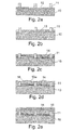
図1はSiGe材料1から成る薄長のストライプを示しており、この材料は、SiGe材料を4辺で取り囲むSi酸化物壁2による包囲領域内で成長する。エピタキシャル成長によるこの領域内でのSiGe層の成長の間、転位3はこの領域の短辺に沿って、すなわち一方の長い方の酸化物壁から他方の反対側の長い方の酸化物壁に向かって優先的に形成される。これらの転位3は長い方の酸化物壁の内の一方又は他方に沿った転位核生成サイト4(各々の核生成サイトを図の「X」で示す)で形成される。これは通常、成長ゾーンの端で転位が形成され易いからである。転位が短辺に沿って形成される場合、これらの転位はほとんど何の抵抗もなくゾーンの反対側に延びることができる。しかしながら、ゾーンの長編に沿って形成されようとする転位は、短辺に沿って形成される転位に直ぐに妨害されるので、ゾーンの全長を横切ることができない。図1に、このような転位5がゾーンの一端から生じ、短辺に沿って延びる転位3によって直ぐにピンニング位置6で阻止された状態が示されている。
FIG. 1 shows a thin stripe of SiGe material 1, which grows in an enclosed region by a
従ってこの場合のSiGe材料は、短辺に沿って延びる転位が形成されることによって一方向の緩和が可能になるだけで、長辺に沿って形成される転位が形成されないので直交方向では緩和されないままである(但し、短辺が十分小さい場合には或る弾性緩和が生じ得る)。上に記載した達成困難な項目を、酸化物壁2内に閉じ込められた小領域内でのSiGeの成長に関して議論したが、同様な問題は、SiGeを基板表面領域により制限される領域内、例えばエッチングにより形成されるメサ構造ピラーの上部の上に成長させる必要がある場合に観察される。
Therefore, the SiGe material in this case can be relaxed in one direction by forming dislocations extending along the short side, and not relaxed in the orthogonal direction because dislocations formed along the long side are not formed. (However, some elastic relaxation may occur if the short side is sufficiently small). While the difficult items described above have been discussed with respect to SiGe growth in a small region confined within the
従って、歪みSi活性層又は歪みSiGe活性層、及び内部にMOSFETのような能動半導体素子を形成することができる歪のないIII−V族半導体活性層の成長に適する緩和SiGe仮想基板を形成する本発明の方法によれば、酸化物層をSi基板10の上に成長させ、次にエッチングすべき領域を画定した後に、例えばフォトレジスト層を酸化物層に塗布し、フォトレジスト層を選択的に露光し、現像してフォトレジストマスクを形成することにより酸化物層を選択的にエッチングする。エッチングの後、図2aに示すように、細長の酸化物壁11が基板10の長さに沿って互いにほぼ平行に延び、薄長の細片12によって分離される。この図では、続いて、SiGe層を上に既に説明した方法で成長させる。
Therefore, a book for forming a relaxed SiGe virtual substrate suitable for growth of a strained Si active layer or strained SiGe active layer and a strain-free III-V group semiconductor active layer in which an active semiconductor element such as a MOSFET can be formed. According to the method of the invention, after an oxide layer is grown on the
続くエピタキシャル成長プロセスでは、図2bに示すように、SiGe層13を酸化物壁11間の薄長の各細片12の上に選択的に、室温〜1,200℃、好適には350〜900℃の温度で成長させる。このようなSiGe成長は、酸化物壁11の上部に沿ったSiGeに成長がほとんど生じないという点で選択的である。このような選択成長は化学的気相成長(CVD)によって行なうことができる。
In the subsequent epitaxial growth process, as shown in FIG. 2b, the
図2cに示すように、転位14は、各酸化物壁11に形成され、且つ反対側の酸化物壁11に向かって短辺に沿って延びるように生じる。このようにして、壁11間の領域の幅全体に渡って延びる転位14の方向にSiGe材料が緩和する。
As shown in FIG. 2 c, the
必要に応じて室温〜1,500℃、好適には500〜1,200℃の高温で実施されるアニール工程によって容易になるこのような緩和に続いて、SiGe材料のエピタキシャル成長が、室温〜1,200℃、好適には350〜900℃の温度で継続して行なわれ、第1SiGe層13に連続する形で更に別のSiGe層13aが形成され、このSiGe層13aの形成は、図2dに示すように、SiGe材料が酸化物壁11の上部を覆う形で横方向に成長するまで行なわれる。最終的に、酸化物壁11の間の領域で種結晶となるSiGeの成長領域が互いに融合し、Si基板の全面を覆う。このようにして成長させたSiGe材料は単結晶層を形成するか、又は異なる成長ゾーンが融合した積層欠陥が生じ得る。いずれにしても、異なる成長ゾーンが接する箇所で表面がでこぼこになる。
Following such relaxation, which is facilitated by an annealing step performed at an elevated temperature of room temperature to 1,500 ° C., preferably 500-1,200 ° C., if necessary, the epitaxial growth of the SiGe material is performed at room temperature to 1, A
SiGeの成長が続くと、緩和されない長さ方向の歪みは最終的には、且つウェハ上の任意の箇所を核として生じ得る長さ方向の転位が形成されることにより緩和される。このような核生成は、成長ゾーンの各辺の酸化物壁による核生成の活性化エネルギーよりもずっと大きい活性化エネルギーを有するので、このような長さ方向の転位15の形成は酸化物壁11により画定される窓の内側での転位14の形成よりもずっと後の段階で生じる。
If the growth of SiGe continues, the strain in the lengthwise direction that is not relaxed is finally relaxed by the formation of dislocations in the lengthwise direction that can occur at any location on the wafer as a nucleus. Such nucleation has an activation energy that is much greater than the activation energy of the nucleation by the oxide walls on each side of the growth zone, so the formation of
長さ方向の転位15は窓の内側の転位14よりも高い位置に形成されるので、この2組の転位14,15は互いに作用することがなく、これらの転位はウェハの全表面を覆って延びることができる。更に、SiGe材料には外部の壁11に直交する方向に歪みが生じないので、この方向に転位を生じさせ易い駆動力が生じない。更に、全ての転位相互作用が最小限に維持されるので、貫通転位がほとんど生じることがない。転位相互作用が生じる場合には貫通転位がSiGe材料の上面で終端することになって表面が粗くなる。
Since the
このようにして、高品質の仮想基板が形成され、このような仮想基板を歪みSi活性層又は歪みSiGe活性層及び内部に能動半導体素子を形成することができる歪みのないIII−V族半導体活性層の成長に使用することができる。 In this way, a high quality virtual substrate is formed, and such a virtual substrate can be formed into a strained Si active layer or a strained SiGe active layer and an active semiconductor element within the strain-free III-V semiconductor activity. Can be used for layer growth.
上述の方法では、SiGe材料のGe組成に応じて酸化物壁11の高さは10nm〜1,000nmの範囲で変化させることができ、普通この高さは400nm〜700nmの範囲が望ましい。酸化物窓の幅は100nm〜100μmとすることができ、5μm〜20μmが最も多く使用される。酸化物壁11の幅はできる限り狭いことが好ましく、これによって横方向に延びて壁を完全に覆う形の成長が保証され、従って現在のところ、幅は100nm〜10μm、好ましくは約1μmである。
In the above-described method, the height of the
SiGe材料内のGe組成は層の厚さ全体に渡ってほぼ一定とすることができるが、Ge組成が層の低い位置の第1組成から層の高い位置の第2の高い組成に増加するようにGe組成を傾斜させることもできる。 The Ge composition in the SiGe material can be approximately constant throughout the thickness of the layer, but as the Ge composition increases from a first composition at a lower position in the layer to a second higher composition at a higher position in the layer. It is also possible to incline the Ge composition.
上に記載した方法の種々の変形を本発明の範囲内で実施することができる。例えば、SiGe材料が十分に成長して酸化物壁11の上部を覆った後、図2dに示すようにでこぼこの表面16が形成され、化学的機械研磨(CMP)工程を実施して表面を平坦化することによりこのでこぼこ表面の影響を無くした後、最終キャップ層を成長させて図2eに示す最終構造を得るとができる。更に別の変形では、アニール工程を実施して確実に全体を緩和させる。このようなアニール工程は、SiGe成長プロセスのどの段階でも実施することができるが、この工程は酸化物壁11の間にSiGeを選択的に成長させた後で、且つSiGeがさらに成長して酸化物壁11の上部を覆う前に実施することが好ましい。
Various variations of the method described above can be implemented within the scope of the present invention. For example, after the SiGe material has grown sufficiently to cover the top of the
更に別の変形では、SiGe材料を酸化物壁の間に成長させるのではなく、成長ゾーンを画定する非常に狭い間隔で配置されたメサ型ピラーの上部にSiGeを成長させる。この場合、細片間の絶縁は、絶縁酸化物壁を使用するのではなく、ピラー間のトレンチを使用して行ない、エピタキシャル成長プロセスを分子線エピタキシ(MBE)又はCVDとすることができる。更に別の構成として、Si窒化物又は他の絶縁材料から成る平行配置された壁の間にSiGe材料を成長させることができる。 In yet another variation, rather than growing SiGe material between oxide walls, SiGe is grown on top of very closely spaced mesa pillars that define a growth zone. In this case, the insulation between the strips can be done using trenches between pillars rather than using insulating oxide walls, and the epitaxial growth process can be molecular beam epitaxy (MBE) or CVD. As a further alternative, SiGe material can be grown between parallel walls of Si nitride or other insulating material.
更に、成長が選択領域にのみ生じるように、パターニングされたシリコンウェハ、又はパターニングされた酸化物層を有するウェハの上に仮想基板をエピタキシャル成長させることができる。従って、この形成技術を使用して、例えば先端回路機能が必要なチップの一つ以上の選択領域(システムオンチップ集積回路設計に必要な領域等)にのみ仮想基板を形成することができる。 Furthermore, a virtual substrate can be epitaxially grown on a patterned silicon wafer or a wafer having a patterned oxide layer so that growth occurs only in selected regions. Therefore, using this formation technique, for example, a virtual substrate can be formed only in one or more selected areas (such as areas necessary for system-on-chip integrated circuit design) of chips that require advanced circuit functions.
本発明の方法は、仮想基板の形成を含む広範囲の用途に適用することができ、仮想基板を形成することによって、歪みを有する、又は歪みが緩和されたSi、Ge又はSiGe層を成長させてバイポーラ接合トランジスタ(BJT)、電界効果トランジスタ(FET)、及び共鳴トンネルダイオード(RTD)のような素子を形成することができるだけでなく、III−V族半導体層を成長させてCMOS技術、及び発光ダイオード(LED)及び半導体レーザを含むオプトエレクトロニクス用途の高速デジタルインターフェースを実現することができる。 The method of the present invention can be applied to a wide range of applications, including the formation of virtual substrates, by forming a virtual substrate to grow a strained or relaxed Si, Ge or SiGe layer. Not only can devices such as bipolar junction transistors (BJT), field effect transistors (FET), and resonant tunneling diodes (RTD) be formed, but also III-V semiconductor layers can be grown to achieve CMOS technology and light emitting diodes. High-speed digital interfaces for optoelectronic applications including (LEDs) and semiconductor lasers can be realized.
Claims (21)
(a)平行配置された絶縁手段(2;11)によってSi表面から成る平行細片(12)を画定する工程、
(b)第1SiGe層(13)を細片(12)の上に選択的に成長させて第1転位(14)が優先的に絶縁手段(2;11)の間の第1SiGe層(13)を横切って延びることにより第1SiGe層(13)の歪みを絶縁手段(2;11)に直交する方向に緩和させる工程、及び
(c)絶縁手段(2;11)を覆うように第1SiGe層(13)の上に第2SiGe層(13a)を成長させ、第2転位(15)が優先的に絶縁手段(2;11)上方の第2SiGe層(13a)の内部に形成されて、第2SiGe層(13a)の歪みを第1転位(14)と直交する方向に緩和する工程
を含む方法。 A method of forming a lattice-adjusted semiconductor substrate,
(A) defining parallel strips (12) consisting of Si surfaces by means of insulating means (2; 11) arranged in parallel;
(B) The first SiGe layer (13) is selectively grown on the strip (12) and the first dislocation (14) is preferentially between the insulating means (2; 11). And the step of relaxing the strain of the first SiGe layer (13) in a direction perpendicular to the insulating means (2; 11) by extending across the first SiGe layer (13), and (c) the first SiGe layer ( A second SiGe layer (13a) is grown on top of 13), and second dislocations (15) are preferentially formed in the second SiGe layer (13a) above the insulating means (2; 11) to form a second SiGe layer. A method comprising a step of relaxing the strain of (13a) in a direction orthogonal to the first dislocation (14).
Applications Claiming Priority (2)
| Application Number | Priority Date | Filing Date | Title |
|---|---|---|---|
| GBGB0220438.6A GB0220438D0 (en) | 2002-09-03 | 2002-09-03 | Formation of lattice-turning semiconductor substrates |
| PCT/GB2003/003514 WO2004023536A1 (en) | 2002-09-03 | 2003-08-12 | Formation of lattice-tuning semiconductor substrates |
Publications (2)
| Publication Number | Publication Date |
|---|---|
| JP2005537672A true JP2005537672A (en) | 2005-12-08 |
| JP2005537672A5 JP2005537672A5 (en) | 2008-12-18 |
Family
ID=9943412
Family Applications (1)
| Application Number | Title | Priority Date | Filing Date |
|---|---|---|---|
| JP2004533596A Pending JP2005537672A (en) | 2002-09-03 | 2003-08-12 | Formation of lattice-adjusted semiconductor substrate |
Country Status (8)
| Country | Link |
|---|---|
| US (1) | US7179727B2 (en) |
| EP (1) | EP1540715A1 (en) |
| JP (1) | JP2005537672A (en) |
| KR (1) | KR20050038037A (en) |
| CN (1) | CN100364052C (en) |
| AU (1) | AU2003251376A1 (en) |
| GB (1) | GB0220438D0 (en) |
| WO (1) | WO2004023536A1 (en) |
Cited By (3)
| Publication number | Priority date | Publication date | Assignee | Title |
|---|---|---|---|---|
| JP2010109358A (en) * | 2008-10-02 | 2010-05-13 | Sumitomo Chemical Co Ltd | Substrate for semiconductor device, semiconductor device equipment, design system, manufacture method and design method |
| WO2010134334A1 (en) * | 2009-05-22 | 2010-11-25 | 住友化学株式会社 | Semiconductor substrate, electronic device, semiconductor substrate manufacturing method, and electronic device manufacturing method |
| WO2017090703A1 (en) * | 2015-11-27 | 2017-06-01 | 国立大学法人東京大学 | METHOD FOR PRODUCING Ge SINGLE CRYSTAL THIN FILM AND OPTICAL DEVICE |
Families Citing this family (23)
| Publication number | Priority date | Publication date | Assignee | Title |
|---|---|---|---|---|
| WO2006011107A1 (en) * | 2004-07-22 | 2006-02-02 | Koninklijke Philips Electronics N.V. | Method of manufacturing a semiconductor device and semiconductor device obtained with such a method |
| GB2418531A (en) * | 2004-09-22 | 2006-03-29 | Univ Warwick | Formation of lattice-tuning semiconductor substrates |
| US9153645B2 (en) | 2005-05-17 | 2015-10-06 | Taiwan Semiconductor Manufacturing Company, Ltd. | Lattice-mismatched semiconductor structures with reduced dislocation defect densities and related methods for device fabrication |
| US8324660B2 (en) | 2005-05-17 | 2012-12-04 | Taiwan Semiconductor Manufacturing Company, Ltd. | Lattice-mismatched semiconductor structures with reduced dislocation defect densities and related methods for device fabrication |
| WO2007112066A2 (en) | 2006-03-24 | 2007-10-04 | Amberwave Systems Corporation | Lattice-mismatched semiconductor structures and related methods for device fabrication |
| US7476606B2 (en) * | 2006-03-28 | 2009-01-13 | Northrop Grumman Corporation | Eutectic bonding of ultrathin semiconductors |
| US8173551B2 (en) | 2006-09-07 | 2012-05-08 | Taiwan Semiconductor Manufacturing Co., Ltd. | Defect reduction using aspect ratio trapping |
| US7875958B2 (en) | 2006-09-27 | 2011-01-25 | Taiwan Semiconductor Manufacturing Company, Ltd. | Quantum tunneling devices and circuits with lattice-mismatched semiconductor structures |
| WO2008051503A2 (en) | 2006-10-19 | 2008-05-02 | Amberwave Systems Corporation | Light-emitter-based devices with lattice-mismatched semiconductor structures |
| US8304805B2 (en) * | 2009-01-09 | 2012-11-06 | Taiwan Semiconductor Manufacturing Company, Ltd. | Semiconductor diodes fabricated by aspect ratio trapping with coalesced films |
| US9508890B2 (en) * | 2007-04-09 | 2016-11-29 | Taiwan Semiconductor Manufacturing Company, Ltd. | Photovoltaics on silicon |
| US8237151B2 (en) * | 2009-01-09 | 2012-08-07 | Taiwan Semiconductor Manufacturing Company, Ltd. | Diode-based devices and methods for making the same |
| US7825328B2 (en) | 2007-04-09 | 2010-11-02 | Taiwan Semiconductor Manufacturing Company, Ltd. | Nitride-based multi-junction solar cell modules and methods for making the same |
| US8329541B2 (en) | 2007-06-15 | 2012-12-11 | Taiwan Semiconductor Manufacturing Company, Ltd. | InP-based transistor fabrication |
| DE112008002387B4 (en) | 2007-09-07 | 2022-04-07 | Taiwan Semiconductor Manufacturing Co., Ltd. | Structure of a multijunction solar cell, method of forming a photonic device, photovoltaic multijunction cell and photovoltaic multijunction cell device, |
| WO2009084238A1 (en) * | 2007-12-28 | 2009-07-09 | Sumitomo Chemical Company, Limited | Semiconductor substrate, method for manufacturing semiconductor substrate, and electronic device |
| US8183667B2 (en) | 2008-06-03 | 2012-05-22 | Taiwan Semiconductor Manufacturing Co., Ltd. | Epitaxial growth of crystalline material |
| US8274097B2 (en) | 2008-07-01 | 2012-09-25 | Taiwan Semiconductor Manufacturing Company, Ltd. | Reduction of edge effects from aspect ratio trapping |
| US8981427B2 (en) | 2008-07-15 | 2015-03-17 | Taiwan Semiconductor Manufacturing Company, Ltd. | Polishing of small composite semiconductor materials |
| US20100072515A1 (en) * | 2008-09-19 | 2010-03-25 | Amberwave Systems Corporation | Fabrication and structures of crystalline material |
| WO2010033813A2 (en) | 2008-09-19 | 2010-03-25 | Amberwave System Corporation | Formation of devices by epitaxial layer overgrowth |
| US8253211B2 (en) | 2008-09-24 | 2012-08-28 | Taiwan Semiconductor Manufacturing Company, Ltd. | Semiconductor sensor structures with reduced dislocation defect densities |
| CN102379046B (en) | 2009-04-02 | 2015-06-17 | 台湾积体电路制造股份有限公司 | Devices formed from a non-polar plane of a crystalline material and method of making the same |
Citations (5)
| Publication number | Priority date | Publication date | Assignee | Title |
|---|---|---|---|---|
| US5158907A (en) * | 1990-08-02 | 1992-10-27 | At&T Bell Laboratories | Method for making semiconductor devices with low dislocation defects |
| JPH04315419A (en) * | 1991-04-12 | 1992-11-06 | Nec Corp | Insulating film/compound semiconductor lamination structure on element semiconductor substrate |
| JPH06260427A (en) * | 1993-03-05 | 1994-09-16 | Nec Corp | Selective growth method of semiconductor film |
| JP2002359189A (en) * | 2001-05-31 | 2002-12-13 | Mitsubishi Materials Silicon Corp | SEMICONDUCTOR SUBSTRATE AND FIELD EFFECT TRANSISTOR, METHOD FOR FORMING SiGe LAYER, METHOD FOR FORMING STRAINED Si LAYER USING IT AND METHOD FOR MANUFACTURING FIELD EFFECT TRANSISTOR |
| JP2004055943A (en) * | 2002-07-23 | 2004-02-19 | Matsushita Electric Ind Co Ltd | Semiconductor device and manufacturing method therefor |
Family Cites Families (13)
| Publication number | Priority date | Publication date | Assignee | Title |
|---|---|---|---|---|
| US5272105A (en) * | 1988-02-11 | 1993-12-21 | Gte Laboratories Incorporated | Method of manufacturing an heteroepitaxial semiconductor structure |
| GB2215514A (en) * | 1988-03-04 | 1989-09-20 | Plessey Co Plc | Terminating dislocations in semiconductor epitaxial layers |
| US5238869A (en) * | 1988-07-25 | 1993-08-24 | Texas Instruments Incorporated | Method of forming an epitaxial layer on a heterointerface |
| EP0380815B1 (en) | 1989-01-31 | 1994-05-25 | Agfa-Gevaert N.V. | Integration of GaAs on Si substrate |
| US5442205A (en) * | 1991-04-24 | 1995-08-15 | At&T Corp. | Semiconductor heterostructure devices with strained semiconductor layers |
| JP3286920B2 (en) * | 1992-07-10 | 2002-05-27 | 富士通株式会社 | Method for manufacturing semiconductor device |
| US6039803A (en) * | 1996-06-28 | 2000-03-21 | Massachusetts Institute Of Technology | Utilization of miscut substrates to improve relaxed graded silicon-germanium and germanium layers on silicon |
| US20010006249A1 (en) | 1997-09-16 | 2001-07-05 | Eugene A Fitzgerald | Co-planar si and ge composite substrate and method of producing same |
| DE19802977A1 (en) | 1998-01-27 | 1999-07-29 | Forschungszentrum Juelich Gmbh | Single crystal layer production on a non-lattice-matched single crystal substrate in microelectronic or optoelectronics component manufacture |
| JP3587081B2 (en) | 1999-05-10 | 2004-11-10 | 豊田合成株式会社 | Method of manufacturing group III nitride semiconductor and group III nitride semiconductor light emitting device |
| US6635110B1 (en) * | 1999-06-25 | 2003-10-21 | Massachusetts Institute Of Technology | Cyclic thermal anneal for dislocation reduction |
| JP4406995B2 (en) * | 2000-03-27 | 2010-02-03 | パナソニック株式会社 | Semiconductor substrate and method for manufacturing semiconductor substrate |
| JP4269541B2 (en) | 2000-08-01 | 2009-05-27 | 株式会社Sumco | Semiconductor substrate, field effect transistor, method of forming SiGe layer, method of forming strained Si layer using the same, and method of manufacturing field effect transistor |
-
2002
- 2002-09-03 GB GBGB0220438.6A patent/GB0220438D0/en not_active Ceased
-
2003
- 2003-08-12 AU AU2003251376A patent/AU2003251376A1/en not_active Abandoned
- 2003-08-12 EP EP03793846A patent/EP1540715A1/en not_active Withdrawn
- 2003-08-12 JP JP2004533596A patent/JP2005537672A/en active Pending
- 2003-08-12 WO PCT/GB2003/003514 patent/WO2004023536A1/en active Application Filing
- 2003-08-12 CN CNB038209543A patent/CN100364052C/en not_active Expired - Fee Related
- 2003-08-12 KR KR1020057003640A patent/KR20050038037A/en not_active Application Discontinuation
- 2003-08-12 US US10/525,987 patent/US7179727B2/en not_active Expired - Fee Related
Patent Citations (5)
| Publication number | Priority date | Publication date | Assignee | Title |
|---|---|---|---|---|
| US5158907A (en) * | 1990-08-02 | 1992-10-27 | At&T Bell Laboratories | Method for making semiconductor devices with low dislocation defects |
| JPH04315419A (en) * | 1991-04-12 | 1992-11-06 | Nec Corp | Insulating film/compound semiconductor lamination structure on element semiconductor substrate |
| JPH06260427A (en) * | 1993-03-05 | 1994-09-16 | Nec Corp | Selective growth method of semiconductor film |
| JP2002359189A (en) * | 2001-05-31 | 2002-12-13 | Mitsubishi Materials Silicon Corp | SEMICONDUCTOR SUBSTRATE AND FIELD EFFECT TRANSISTOR, METHOD FOR FORMING SiGe LAYER, METHOD FOR FORMING STRAINED Si LAYER USING IT AND METHOD FOR MANUFACTURING FIELD EFFECT TRANSISTOR |
| JP2004055943A (en) * | 2002-07-23 | 2004-02-19 | Matsushita Electric Ind Co Ltd | Semiconductor device and manufacturing method therefor |
Cited By (5)
| Publication number | Priority date | Publication date | Assignee | Title |
|---|---|---|---|---|
| JP2010109358A (en) * | 2008-10-02 | 2010-05-13 | Sumitomo Chemical Co Ltd | Substrate for semiconductor device, semiconductor device equipment, design system, manufacture method and design method |
| WO2010134334A1 (en) * | 2009-05-22 | 2010-11-25 | 住友化学株式会社 | Semiconductor substrate, electronic device, semiconductor substrate manufacturing method, and electronic device manufacturing method |
| JP2011009718A (en) * | 2009-05-22 | 2011-01-13 | Sumitomo Chemical Co Ltd | Semiconductor substrate, electronic device, method of manufacturing semiconductor substrate, and method of manufacturing electronic device |
| US8890213B2 (en) | 2009-05-22 | 2014-11-18 | Sumitomo Chemical Company, Limited | Semiconductor wafer, electronic device, a method of producing semiconductor wafer, and method of producing electronic device |
| WO2017090703A1 (en) * | 2015-11-27 | 2017-06-01 | 国立大学法人東京大学 | METHOD FOR PRODUCING Ge SINGLE CRYSTAL THIN FILM AND OPTICAL DEVICE |
Also Published As
| Publication number | Publication date |
|---|---|
| AU2003251376A1 (en) | 2004-03-29 |
| EP1540715A1 (en) | 2005-06-15 |
| WO2004023536A1 (en) | 2004-03-18 |
| KR20050038037A (en) | 2005-04-25 |
| CN100364052C (en) | 2008-01-23 |
| CN1714427A (en) | 2005-12-28 |
| US7179727B2 (en) | 2007-02-20 |
| US20050245055A1 (en) | 2005-11-03 |
| GB0220438D0 (en) | 2002-10-09 |
Similar Documents
| Publication | Publication Date | Title |
|---|---|---|
| JP2005537672A (en) | Formation of lattice-adjusted semiconductor substrate | |
| US20200194559A1 (en) | Lattice-Mismatched Semiconductor Structures with Reduced Dislocation Defect Densities and Related Methods for Device Fabrication | |
| CN1216405C (en) | Semiconductor substrate, field effect transistor, and method for forming silicon germanide layer | |
| JP5122130B2 (en) | Method for forming a stress relaxation layer structure on a substrate that is not lattice matched | |
| JP5508982B2 (en) | Shallow trench isolation process | |
| JP2005528795A (en) | Formation of lattice-matched semiconductor substrates | |
| EP1687841B1 (en) | Formation of lattice-tuning semiconductor substrates | |
| JP2007326771A (en) | Forming method and compound semiconductor wafer | |
| US20060081932A1 (en) | Semiconductor channel on insulator structure | |
| JPH0766366A (en) | Semiconductor multilayered structure and semiconductor device using same | |
| JPH10256169A (en) | Manufacture of semiconductor device | |
| US20070212879A1 (en) | Formation of lattice-tuning semiconductor substrates | |
| JP2516316B2 (en) | Three-dimensional silicon silicide structure | |
| JP4039013B2 (en) | Semiconductor substrate, field effect transistor, method of forming SiGe layer, method of forming strained Si layer using the same, and method of manufacturing field effect transistor | |
| US5341000A (en) | Thin silicon carbide layer on an insulating layer | |
| JP4254102B2 (en) | Semiconductor substrate, field effect transistor, and manufacturing method thereof | |
| JP4221928B2 (en) | Semiconductor substrate, field effect transistor, and manufacturing method thereof | |
| KR20050024669A (en) | Semiconductor wafer having guardring layer and method for manufacturing the same |
Legal Events
| Date | Code | Title | Description |
|---|---|---|---|
| A621 | Written request for application examination |
Free format text: JAPANESE INTERMEDIATE CODE: A621 Effective date: 20060711 |
|
| A711 | Notification of change in applicant |
Free format text: JAPANESE INTERMEDIATE CODE: A711 Effective date: 20061016 |
|
| A521 | Request for written amendment filed |
Free format text: JAPANESE INTERMEDIATE CODE: A523 Effective date: 20081027 |
|
| A131 | Notification of reasons for refusal |
Free format text: JAPANESE INTERMEDIATE CODE: A131 Effective date: 20101005 |
|
| A02 | Decision of refusal |
Free format text: JAPANESE INTERMEDIATE CODE: A02 Effective date: 20110322 |