JP4288743B2 - Nitride semiconductor growth method - Google Patents
Nitride semiconductor growth method Download PDFInfo
- Publication number
- JP4288743B2 JP4288743B2 JP08028899A JP8028899A JP4288743B2 JP 4288743 B2 JP4288743 B2 JP 4288743B2 JP 08028899 A JP08028899 A JP 08028899A JP 8028899 A JP8028899 A JP 8028899A JP 4288743 B2 JP4288743 B2 JP 4288743B2
- Authority
- JP
- Japan
- Prior art keywords
- nitride semiconductor
- substrate
- growth
- protective film
- grown
- Prior art date
- Legal status (The legal status is an assumption and is not a legal conclusion. Google has not performed a legal analysis and makes no representation as to the accuracy of the status listed.)
- Expired - Fee Related
Links
Images


Classifications
-
- H—ELECTRICITY
- H01—ELECTRIC ELEMENTS
- H01S—DEVICES USING THE PROCESS OF LIGHT AMPLIFICATION BY STIMULATED EMISSION OF RADIATION [LASER] TO AMPLIFY OR GENERATE LIGHT; DEVICES USING STIMULATED EMISSION OF ELECTROMAGNETIC RADIATION IN WAVE RANGES OTHER THAN OPTICAL
- H01S2304/00—Special growth methods for semiconductor lasers
- H01S2304/12—Pendeo epitaxial lateral overgrowth [ELOG], e.g. for growing GaN based blue laser diodes
-
- H—ELECTRICITY
- H01—ELECTRIC ELEMENTS
- H01S—DEVICES USING THE PROCESS OF LIGHT AMPLIFICATION BY STIMULATED EMISSION OF RADIATION [LASER] TO AMPLIFY OR GENERATE LIGHT; DEVICES USING STIMULATED EMISSION OF ELECTROMAGNETIC RADIATION IN WAVE RANGES OTHER THAN OPTICAL
- H01S5/00—Semiconductor lasers
- H01S5/02—Structural details or components not essential to laser action
- H01S5/0206—Substrates, e.g. growth, shape, material, removal or bonding
-
- Y—GENERAL TAGGING OF NEW TECHNOLOGICAL DEVELOPMENTS; GENERAL TAGGING OF CROSS-SECTIONAL TECHNOLOGIES SPANNING OVER SEVERAL SECTIONS OF THE IPC; TECHNICAL SUBJECTS COVERED BY FORMER USPC CROSS-REFERENCE ART COLLECTIONS [XRACs] AND DIGESTS
- Y02—TECHNOLOGIES OR APPLICATIONS FOR MITIGATION OR ADAPTATION AGAINST CLIMATE CHANGE
- Y02E—REDUCTION OF GREENHOUSE GAS [GHG] EMISSIONS, RELATED TO ENERGY GENERATION, TRANSMISSION OR DISTRIBUTION
- Y02E10/00—Energy generation through renewable energy sources
- Y02E10/50—Photovoltaic [PV] energy
Description
【0001】
【発明の属する技術分野】
本発明は窒化物半導体(InXAlYGa1-X-YN、0≦X、0≦Y、X+Y≦1)の成長方法に係り、特に転位の少ない窒化物半導体の成長方法に関する。また、本発明は、前記窒化物半導体よりなる基板を用い発光ダイオード、レーザダイオード等の発光素子、あるいは太陽電池、光センサー等の受光素子に使用される窒化物半導体(InXAlYGa1-X-YN、0≦X、0≦Y、X+Y≦1)よりなる窒化物半導体素子に関する。
【0002】
【従来の技術】
近年、窒化物半導体からなる青色、青緑色の発光ダイオード(LED)、レーザダイオード(LD)が実用化されたり実用可能になっている。
【0003】
例えば、本発明者等は、Aplide Physics Letters. Vol.73, Number6 (1998) pp.832-834 に、サファイア上に、有機金属化学気相成長法(MOCVD)により2μmの膜厚で成長させたGaN層上に、0.1μmの膜厚のSiO2よりなる保護膜を部分的に形成し、その後、保護膜を有する面上に再度GaNをMOCVDにより20μmの膜厚で成長(ELOG成長)させ、続いて、ハイドライド気相成長法(HVPE)により200μmの膜厚のGaNを成長させ、その後サファイア基板を研磨により除去して、ほぼ150μmの膜厚のGaNの基板を得て、このGaN基板上にデバイス構造を形成し、GaN基板のM面[六方晶系の側面;例えば{1−100}等]で劈開して共振面を形成してなる窒化物半導体素子を報告している。
そして、報告されたレーザ素子は、劈開により形成された共振面からのレーザ光のファーフィールドパターンが良好で、また出力5mWとなるように動作電流を調整し50℃の条件下でほぼ180時間の連続発振が可能となる。
【0004】
【発明が解決しようとする課題】
しかしながら、上記Appl.Phys.Lett.に報告されている窒化物半導体素子は、レーザ素子の実用化の可能性を有しているものの、実用化のためには寿命特性が十分満足できるものではない。上記報告されているレーザ素子は、高温でかなりの長時間、連続発振できるが、連続発振が180時間を過ぎると、動作電流が急激に増加することから、素子の劣化がかなり進行していると推測できる。
【0005】
本発明者等は、寿命特性のさらなる向上のために種々検討した結果、デバイス構造を成長させる窒化物半導体基板の表面に、表面透過型電子顕微鏡(表面TEM)観察によると、ほぼ均一に1×10⁷個/cm2程度の転位が確認され、この転位により寿命特性が低下するのではないかと考えた。上記転位密度は、従来のサファイア基板上にGaNを成長させていく場合に比べれば、かなり低減されているが、実用化に際しての素子の信頼性を十分にするには、寿命特性をさらに向上させる必要がある。
【0006】
窒化物半導体基板の表面にほぼ均一に転位が見られる原因として、劈開の際の物理的強度を向上させ欠けや割れを防止するため、HVPEで膜厚200μmの厚さに窒化物半導体を成長させる過程で、保護膜の形成されていない部分(窓部)上部に見られる転位が、窒化物半導体の成長と共に均一に広がっているためと推測できる。
【0007】
ちなみに、保護膜を形成後、MOCVDで20μmの膜厚で窒化物半導体を成長させた時点では、窓部上部にはほぼ1×10⁹個/cm2程度の転位が見られるが、一方、保護膜上部にはほとんど転位が見られない。仮に、この転位のない保護膜上部にデバイス構造、特にリッジ形状のストライプを形成すると、寿命特性が向上する。しかし、20μmの膜厚の窒化物半導体からサファイアを除去して、劈開により共振面を形成するには、20μmの膜厚の窒化物半導体基板では物理的強度が十分でなく、欠けや割れが生じ歩留まりが低下する。さらに、デバイス構造を形成する際にも窒化物半導体基板の物理的強度が必要である。
このように、サファイアを除去して窒化物半導体のみの基板上に、デバイス構造を形成することは、鏡面状の共振面を得ることができる劈開という簡易な方法を可能にするものの、劈開時及びデバイス工程時の物理的強度が十分となる程度の膜厚に成長させなければならず、このため、ELOG成長で得られた転位のほとんどない部分が窒化物半導体基板表面から失われてしまう。
以上のように、レーザ素子の寿命特性の向上には、デバイス構造を形成するための窒化物半導体基板の転位密度をより一層低下させることが望まれる。
【0008】
そこで、本発明の目的は、窒化物半導体を基板とした場合、デバイス構造を形成しても、劈開により共振面を形成しても、基板に欠けやクラックの発生が生じず、更に、寿命特性を良好にでき、実用化に際しての素子の信頼性が向上するような転位の低減される窒化物半導体基板の得られる窒化物半導体の成長方法を提供することである。
更に、本発明の目的は、本発明の窒化物半導体の成長方法により得られる窒化物半導体を基板とし、寿命特性など素子特性の良好な窒化物半導体素子を提供することである。
【0009】
【課題を解決するための手段】
即ち、本発明は、下記(1)〜(13)の構成により、本発明の目的を達成することができる。
(1) 窒化物半導体と異なる材料よりなる異種基板上に成長された窒化物半導体上に、露出された凹凸を形成する工程と、前記露出された凹凸を有する面上に、前記凹凸の凸部上面及び凹部側面からの横方向の成長を利用して第1の窒化物半導体を成長させる工程と、その後、少なくとも前記異種基板を除去することにより、窒化物半導体基板とする工程と、前記窒化物半導体基板の異種基板を除去した面とは反対の面上に、第2の窒化物半導体を成長させる工程とを有することを特徴とする窒化物半導体の成長方法。
(2) 前記窒化物半導体基板は、反りを有することを特徴とする(1)に記載の窒化物半導体の成長方法。
(3) 前記第1の窒化物半導体は、10μm/時間以下0.5μm/時間以上の成長速度で成長させ、前記第2の窒化物半導体は、500μm/時間以下10μm/時間以上の成長速度で成長させることを特徴とする(1)又は(2)に記載の窒化物半導体の成長方法。
(4) 前記第1の窒化物半導体は有機金属化学気相成長法により成長させ、前記第2の窒化物半導体はハイドライド気相成長法により成長させることを特徴とする(1)〜(3)のいずれかに記載の窒化物半導体の成長方法。
(5) 前記凹凸の凹部底部からの縦方向成長に比べ前記凹部側面からの横方向の成長を促進させて、前記第1の窒化物半導体を成長させることを特徴とする(1)〜(4)のいずれかに記載の窒化物半導体の成長方法。
(6) 前記凹部内部で前記凹部側面からの成長を接合させて前記凹部底部からの成長を遮り、前記第1の窒化物半導体を成長させることを特徴とする(1)〜(5)のいずれかに記載の窒化物半導体の成長方法。
(7) p型不純物及び/又はn型不純物をドープすることにより横方向の成長を促進させて、前記第1の窒化物半導体を成長させることを特徴とする(1)〜(6)のいずれかに記載の窒化物半導体の成長方法。
(8) 前記第1及び第2の窒化物半導体はアンドープのGaNからなることを特徴とする(1)〜(6)のいずれかに記載の窒化物半導体の成長方法。
(9) 前記凹凸が、前記窒化物半導体基板のM軸方向、<1−100>、<10−10>及び<01−10>のいずれかのM軸方向に対して平行方向となるように形成されたストライプ形状であることを特徴とする(1)〜(8)のいずれかに記載の窒化物半導体の成長方法。
(10) 前記第1の窒化物半導体を成長させた後、該第1の窒化物半導体上に、第3の窒化物半導体を成長させる工程を有し、前記窒化物半導体基板が、少なくとも第3の窒化物半導体からなることを特徴とする(1)〜(9)のいずれかに記載の窒化物半導体の成長方法。
(11) 前記異種基板を除去する工程において、異種基板から第3の窒化物半導体の一部までを除去することを特徴とする(10)に記載の窒化物半導体の成長方法。
(12) 前記窒化物半導体基板が、その表面の転位密度が1010個/cm2以下であることを特徴とする(1)〜(11)のいずれかに記載の窒化物半導体の成長方法。
(13) 前記窒化物半導体基板が、50〜1000μmの膜厚を有することを特徴とする請求項(1)〜(12)のいずれかに記載の窒化物半導体の成長方法。
また、本発明は、下記(14)〜(16)の構成とすることができる。
(14) 前記(1)〜(13)のいずれかに記載の窒化物半導体の成長方法により得られた転位の低減された窒化物半導体を基板として、この窒化物半導体基板上に、少なくとn型窒化物半導体、活性層、及びp型窒化物半導体を有するデバイス構造が形成されてなることを特徴とする窒化物半導体素子。
(15) 前記窒化物半導体素子が、ストライプ形状の保護膜又はストライプ形状の凹凸の、ストライプ方向に平行に形成されたリッジ形状のストライプを有することを特徴する(14)に記載の窒化物半導体素子。
(16) 前記窒化物半導体素子のリッジ形状のストライプが、ストライプ形状の保護膜の上部、又はストライプ形状の凹凸の凹部上部に形成されていることを特徴とする(14)又は(15)に記載の窒化物半導体素子。
【0010】
つまり、本発明の成長方法は、デバイス構造を形成可能な程度の厚膜の窒化物半導体基板上に、上記の如く、第5の工程においてELOG成長させることにより、表面の転位を低減し、特に表面にほとんど転位の見られない部分を有する第4の窒化物半導体を成長させることにより、劈開しても欠けや割れが発生し難く、且つ転位のほとんどない部分を有しているので素子の劣化を防止でき寿命特性を向上できる良好な基板を提供することができる。
上記基板は、デバイス構造を形成するための基板であり、本発明においては、第5の工程における窒化物半導体基板と転位の低減された第4の窒化物半導体とからなるものが、デバイス構造を形成するための基板となる。以下単に本発明の基板とする場合がある。
【0011】
従来、前記課題で示したように、転位を低減する試みは、デバイス構造を形成するための基板として、窒化物半導体を厚膜に成長させる工程の前段階で転位の伝播を抑制したり止めたりする試みが種々行われている。
【0012】
これに対して、本発明は、デバイス構造を形成可能な程度に厚膜に成長された窒化物半導体基板上に、従来の知見から考えると一見製造工程を複雑化、長時間化しているように思われるようなELOG成長を行うことにより、前記課題を解決することができる。
窒化物半導体基板上にELOG成長をすることで得られる第4の窒化物半導体は、転位密度が低減され、さらには転位がほとんどない部分を有している。この窒化物半導体基板と第4の窒化物半導体とからなる本発明の基板は、厚膜の窒化物半導体基板により物理的強度が得られ、さらに本発明の基板の第4の窒化物半導体上にデバイス構造を形成すると、寿命特性の向上が可能となる。
本発明の方法は、前記したように一見製造工程を煩雑にしてしているように思われるが、本発明の基板を用いることで寿命特性の向上が可能となると共に、割れや欠けが防止され歩留まりの向上が可能となり、製造工程を総合的に考慮した場合、製造効率の向上につながる。
【0013】
本発明の課題は、上記Appl.Phys.Lett.での報告のように、転位の低減された厚膜の窒化物半導体を基板とし、この上にデバイス構造を形成してなるレーザ素子が、かなりの長時間の連続発振を達成できたことによって、実用化の達成や信頼性の向上のために解決しなければならない問題点として新たに見出されたものである。
このことから、たとえ、窒化物半導体基板上にデバイス構造を形成してなる窒化物半導体素子であっても、得られた素子が長時間の連続発振をすることができないような素子からは、基板の転位が寿命特性へどのように影響するかといったような本発明の課題を新たに見出すことは困難である。
【0014】
また更に、本発明において、第5の工程における窒化物半導体の横方向の成長を利用して転位の低減される方法(以下、第5の工程のELOG成長と言う場合がある。)が、窒化物半導体基板上に第2の保護膜を部分的に形成し、その後、第2の保護膜の形成面上に第4の窒化物半導体を成長させてなると、転位の進行を防止するのに好ましい。
また更に、本発明において、第2の保護膜が、窒化物半導体基板のM軸方向、<1−100>、<10−10>及び<01−10>のいずれかのM軸方向に対して平行方向に形成されたストライプ形状であると、窒化物半導体の横方向の成長を促進でき転位の伝播を抑制するのに好ましい。更に第2の保護膜が、後述のストライプ形状の第1の保護膜又はストライプ形状の第1の凹凸と平行に形成されていると、第4の窒化物半導体の横方向の成長がより良好となり、第4の窒化物半導体上を良好に得ることができ、転位の低減でも好ましい。
【0015】
また更に、本発明において、第5の工程のELOG成長が、窒化物半導体基板の表面に第2の凹凸を形成するのみで、その第2の凹凸を有する面上に第4の窒化物半導体を成長させると、転位の伝播を抑制する点で好ましい。この場合は、上記のような第2の保護膜を用いない。
また更に、本発明において、第2の凹凸が、窒化物半導体基板のM軸方向、<1−100>、<10−10>及び<01−10>のいずれかのM軸方向に対して平行方向に形成されたストライプ形状であると、窒化物半導体の横方向の成長を促進でき転位の伝播を抑制するのに好ましい。
【0016】
また更に、本発明において、第5の工程で用いられる窒化物半導体基板が、その表面の転位密度が1010個/cm2以下のものであると、窒化物半導体基板上にELOG成長させて得られる第4の窒化物半導体の表面に現れる転位を低減するのに好ましい。
また更に、本発明において、前記窒化物半導体基板が、50μm〜1000μmの膜厚を有すると、デバイス工程や劈開工程での物理的強度が良好となり、窒化物半導体基板の欠けや割れ等が防止され、素子を量産する場合の歩留まりの向上の点で好ましい。
【0017】
更に本発明において、窒化物半導体基板が、上記第1の工程〜第3の工程から得られる少なくとも第3の窒化物半導体からなるものであると、第3の窒化物半導体の表面には既に転位がある程度低減されているので、この第3の窒化物半導体の上にELOG成長させて得られる第4の窒化物半導体の表面には更に転位が低減され好ましい。また、第3の窒化物半導体を成長させる際に、成長速度の速い方法により成長させると、第3の窒化物半導体を厚膜に成長させても異常成長の発生が起こりにくい。
ここで、第5の工程における、第4の窒化物半導体は、第3の窒化物半導体の異種基板を除去した面とは反対の面上に成長させる。
【0018】
更に、本発明において、窒化物半導体基板が、前記第3の工程後に、第4の工程を経て得られる第3の窒化物半導体とその上に成長された第2の窒化物半導体とからなるものであると、反りが軽減され、第5の工程のELOG成長を行うのに好ましい。つまり、異種基板を除去すると、第3の窒化物半導体の成長面と除去面との面状態が異なるため、第3の窒化物半導体に反りが発生する傾向が見られる場合があるが、第3の窒化物半導体の成長面(異種基板の除去面とは反対の面)に第2の窒化物半導体を成長させると、第3の窒化物半導体の反りが軽減される。また異種基板を除去後に第2の窒化物半導体を成長させることで、窒化物半導体基板の物理的強度を補強することができる。
【0019】
更に本発明において、第1の工程でのELOG成長が、異種基板上に成長された窒化物半導体上に、第1の保護膜を部分的に形成して第1の窒化物半導体を成長させる工程、又は異種基板上に成長された窒化物半導体上に、第1の凹凸を形成して第1の窒化物半導体を成長させる工程、であると窒化物半導体基板の転位が低減でき、転位の少ない第4の窒化物半導体を成長させるのに好ましい。
更に本発明において、第1の工程で形成される第1の保護膜又は第1の凹凸が、前記窒化物半導体基板の<1−100>、<10−10>及び<01−10>のいずれかのM軸方向に対して平行方向となるように形成されたストライプ形状であり、且つ、第5の工程で形成される第2の保護膜又は第2の凹凸と平行となるように形成されていると、窒化物半導体の横方向の成長がより促進され窒化物半導体基板の転位を低減するのに好ましいと共に、第5の工程で窒化物半導体基板上に成長される第4の窒化物半導体の横方向の成長がより良好となり、転位の低減の点で好ましい。
【0020】
ここで、第2の保護膜などを形成する際には、既に第1の保護膜などは除去されているが、窒化物半導体基板の異種基板を除去した面には、転位分布がストライプ状に観測され、このストライプ状の転位分布に沿って第1の保護等を形成する。このように形成することにより、第2の保護膜と第1の保護膜、あるは第2の保護膜と第1の凹凸、第2の凹凸と第1の保護膜、第2の凹凸と第1の凹凸等がそれぞれ窒化物半導体のM軸方向に平行となる。
またオリエンテーションフラット面(オリフラ面)が窒化物半導体のM軸方向に垂直となるようにし、このオリフラ面を基準にすることで、第5の工程と第1の工程で用いられる保護膜や凹凸が平行方向のストライプ形状として形成可能である。
【0021】
また、本発明において、上記本発明の窒化物半導体の成長方法により得られる転位の低減された窒化物半導体(窒化物半導体基板と第4の窒化物半導体とからなる)を基板として、この基板上に、少なくともn型窒化物半導体、活性層、及びp型窒化物半導体を有するデバイス構造が形成されてなると、寿命特性などの素子特性が良好な窒化物半導体素子を提供することができる。
また更に、本発明において、窒化物半導体素子が、ストライプ形状の第2の保護膜又はストライプ形状の第2の凹凸の、ストライプ方向に平行に形成されたリッジ形状のストライプを有すると、窒化物半導体基板のM軸方向に垂直な面での劈開により良好な鏡面状の共振面が得られファーフィールドパターンが良好となり好ましい。
また更に、本発明において、窒化物半導体素子のリッジ形状のストライプが、第2の保護膜の上部、又は第2の凹凸の凹部上部に形成されていると、これらの部分には第4の窒化物半導体の表面での転位が最も少なくなる傾向があるため、素子の劣化が防止され、寿命特性の向上の点で好ましい。
【0022】
本発明において、後述の説明の中のアンドープとは、意図的に不純物をドープしないで形成した層を示し、隣接する層からの不純物の拡散、原料又は装置からのコンタミネーションにより不純物が混入した層であっても、意図的に不純物をドープしていない場合はアンドープ層とする。
【0023】
【発明の実施の形態】
以下に図1〜5を用いて本発明を詳細に説明する。
まず図1(a)〜(d)は、本発明の窒化物半導体の成長方法により得られるデバイス構造を形成するための基板の模式的断面図を示している。この図1を用いて、本発明の第5の工程を有する窒化物半導体の成長方法を説明する。
【0024】
本発明の窒化物半導体の成長方法は、第5の工程により、窒化物半導体基板1上に、窒化物半導体の横方向の成長を利用して転位の低減される方法(第5の工程のELOG成長)により、転位の低減された第4の窒化物半導体2を得ることができる。
第5の工程において、第4の窒化物半導体2を成長させる第5の工程のELOG成長としては、窒化物半導体の横方向の成長を利用して転位を低減させる方法であれば特に限定されず、成長のいずれかの段階で、窒化物半導体の縦方向の成長速度に対して、窒化物半導体の横方向の成長速度が促進され、転位の伝播が抑制されるような方法が挙げられる。
転位がどのように伝播するかは定かではないが、転位は窒化物半導体の成長の方向に沿って伝播する傾向があり、窒化物半導体の横方向の成長が促進されると横方向に伝播し、一旦横方向に伝播した転位は再び縦方向に伝播しにくくなる傾向があると思われる。その結果、転位の低減された第4の窒化物半導体を成長させることができると推測される。
【0025】
第5の工程のELOG成長としては、従来公知の厚膜の窒化物半導体基板を成長させる前工程で行われるELOG成長などを用いてもよく、また本出願人が出願した例えば特願平10−77245、同10−275826、同10−119377、同10−132831、同11−37827、同11−37826、同10−146431各号の明細書等に記載されているELOG成長などを用いることができる。但し、これらのELOG成長は、異種基板上で行われているのに対し、本発明の第5の工程のELOG成長は、厚膜の窒化物半導体基板上で行われる点が異なっているが、ほぼ同様に行うことができる。
【0026】
本発明の第5の工程のELOG成長の好ましい具体例としては、窒化物半導体基板上に窒化物半導体が成長しにくいか、又は成長しない材料からなる第2の保護膜11を用いる方法、又は、窒化物半導体基板に第2の凹凸13を形成して行う方法などがあげられる。このように第2の保護膜11や第2の凹凸13を形成し、この形成面に第4の窒化物半導体2を成長させると、第4の窒化物半導体2の成長過程のいずれかの段階で、窒化物半導体の縦方向の成長に対して、窒化物半導体の横方向の成長が促進され、転位が窒化物半導体の横方向の成長と共に横方向へ進行し、再び縦方向に進行しにくくなり、その結果、転位の低減された第4の窒化物半導体2を得ることができると考えられる。
【0027】
このようにして得られた第4の窒化物半導体2表面の平均の転位密度は、窒化物半導体基板表面の平均の転位密度に対して、ほぼ1/100以下程度に減少し、好ましい条件では、第4の窒化物半導体2の表面にはほとんど転位が見られなくなる。
また、第4の窒化物半導体2表面の転位の分布は、第2の保護膜11上部又は第2の凹凸13の凹部上部が、その他の部分(窓部上部又は凸部上部)に比べ極めて転位が少なくなり、表面TEMやカソードルミネッセンス(CL)などの観察によるとほとんど転位が見られなくなる。
このように第4の窒化物半導体2の平均の転位密度が減少すれば、第4の窒化物半導体2上に形成させる素子の寿命特性の向上が可能となり、更に、ほとんど転位のない部分に、素子のリッジ形状のストライプを形成すると、素子の寿命特性の飛躍的な向上が可能となる。
第4の窒化物半導体2の表面の転位密度は、第5の工程で行われるELOG成長の種類にもよるが、平均の転位密度としては1×10⁵個/cm3以下、好ましい条件では1×104個/cm3以下、より好ましい条件では1×103個/cm3以下となる。また、第2の保護膜11上部の転位密度、及び第2の凹凸13の凹部上部の転位は、ほとんど見られなくなる傾向がある。また窓部上部、及び第2の凹凸13の凸部上部の転位密度は、1×107個/cm3以下、好ましい条件では1×106個/cm3以下、より好ましい条件では1×105個/cm3以下となる。
本発明において、転位密度の測定は、表面TEM又はCL等により観察する。
【0028】
以下にELOG成長が第2の保護膜11を用いて行われる場合と、第2の凹凸13を形成して行われる場合の、それぞれの一実施の形態により得られる窒化物半導体基板1と第4の窒化物半導体2とからなるデバイス構造を形成する基板の模式的断面図である図1(a)〜(d)を用いてさらに詳細に説明する。図1(a)〜(c)は第2の保護膜11を用いて行う形態であり、図1(d)は第2の凹凸13を形成して行う形態である。また、第2の保護膜11を用いる形態で、凹凸を形成しこの凹部底部及び/又は凸部上部に保護膜を形成する場合があるが、このような形態も第2の保護膜を形成して行う場合として以下に説明する。
まず図1(a)は、窒化物半導体基板1上に第2の保護膜11を形成し、この形成面上に第4の窒化物半導体2を成長させてなる模式的断面図である。
図1(b)は、窒化物半導体基板1に凹凸を形成し、この凹部底部及び凸部上部に第2の保護膜11を形成し、この形成面上に第4の窒化物半導体2を成長させてなる模式的断面図である。
図1(c)は、窒化物半導体基板1に凹凸を形成し、この凸部上部にのみ第2の保護膜11を形成し、この形成面上に第4の窒化物半導体2を成長させてなる模式的断面図である。
図1(d)は、窒化物半導体基板1に第2の凹凸13を形成し、この形成面上に第4の窒化物半導体2を成長させてなる模式的断面図である。図1(d)では、保護膜を用いずに行う形態である。
【0029】
上記ELOG成長により得られる第4の窒化物半導体2としては、特に限定されないが、好ましくはGaNからなる窒化物半導体である。第4の窒化物半導体2は、アンドープでも不純物をドープされてもよい。アンドープであると結晶性の点で好ましく、またELOG成長の際にp型不純物(Be、Zn、Mn、Cr及びMg)、及びn型不純物(Si、Ge及びSn)のいずれか1種以上、好ましくはp型不純物の少なくとも1種以上、より好ましくはp型不純物の少なくとも1種以上とn型不純物の少なくとも1種以上、最も好ましくはMgとSiとをドープすると、窒化物半導体の横方向の成長が促進され、転位の低減及び空隙発生の防止の点で好ましい。不純物のドープ量としては、好ましくは1×10¹⁷/cm3〜1×1019/cm3、より好ましくは1×1017/cm3〜1×1019/cm3、更に好ましくは5×1017/cm3〜5×1019/cm3である。不純物の濃度が上記範囲であると窒化物半導体の横方向の成長を縦方向の成長に比べ良好に促進でき、結晶欠陥の伝播の抑制及び空隙の発生の防止の点で好ましい。p型不純物とn型不純物とをドープする場合は、両者の濃度の和が上記範囲のドープ量となるように適宜調整してドープされる。この場合p型不純物とn型不純物の濃度の比は、用いる不純物の種類により、空隙や転位を良好に防止できるように適宜調整される。
また、第4の窒化物半導体2にn電極を形成する場合には、n型不純物をドープする、n型不純物をp型不純物より多めにドープする等、n型不純物とp型不純物のドープ量を調整する。
【0030】
第4の窒化物半導体2の膜厚としては、特に限定されないが、好ましくは5μm〜50μmであり、より好ましくは10μm〜35μmである。第4の窒化物半導体2の膜厚が上記範囲であると、窒化物半導体基板1に形成された第2の保護膜11や第2の凹凸13を良好に覆うことができ、窒化物半導体基板1の表面の転位密度より第4の窒化物半導体2の表面の転位密度が少なくなり、更に第4の窒化物半導体2の表面の転位分布で、特に第2の保護膜11上部及び第2の凹凸13の凹部上部にはほとんど転位が見られなくなる。
【0031】
図1(a)〜(c)の第2の保護膜11の材料としては、第2の保護膜11表面に窒化物半導体が成長しないか、又は成長しにくい性質を有する材料が好ましく、例えば酸化ケイ素(SiOX)、窒化ケイ素(SiXNY)、酸化チタン(TiOX)、酸化ジルコニウム(ZrOX)等の酸化物、窒化物、またこれらの多層膜の他、1200℃以上の融点を有する金属等を用いることができる。これらの保護膜材料は、窒化物半導体の成長温度600℃〜1100℃の温度にも耐え、その表面に窒化物半導体が成長しないか、成長しにくい性質を有している。保護膜材料を窒化物半導体表面に形成するには、例えば蒸着、スパッタ、CVD等の気相製膜技術を用いることができる。
【0032】
まず、図1(a)の場合の第2の保護膜11の形成方法や形状等について説明する。
第2の保護膜11を窒化物半導体基板1上に部分的(選択的)に形成するには、フォトリソグラフィー技術を用いて、所定の形状を有するフォトマスクを作製し、そのフォトマスクを介して、前記材料を気相製膜することにより、所定の形状を有する第2の保護膜11を形成できる。第2の保護膜11の形状は特に問うものではなく、例えばドット、ストライプ、碁盤目状の形状のいずれかの形状、好ましくはストライプの形状が挙げられる。第2の保護膜11がストライプ形状であると、転位の低減された第4の窒化物半導体2を良好に形成することができ好ましい。
【0033】
また、第2の保護膜11は、第2の保護膜11が形成されていない部分(窓部)の表面積より大きくなるように、第2の保護膜11の表面積を調整して形成されることが好ましい。第2の保護膜11の表面積及び窓部の表面積の調整は、保護膜の形状によっても異なるが、例えば保護膜がストライプ状の形状の場合、保護膜のストライプの幅と窓部の幅を調整することにより行うことができる。
【0034】
第2の保護膜11の大きさは、特に限定されないが、例えばストライプで形成した場合、好ましいストライプ幅は0.5〜100μm、より好ましくは1μm〜50μm、更に好ましくは2〜25μmである。
また、ストライプピッチ(第2の保護膜11が形成されていない窓部の幅)は、ストライプ幅よりも狭くすることが望ましく、例えば具体的には5μm以下、好ましくは0.1〜3μm、より好ましくは0.8〜2μmである。
【0035】
上記のように、第2の保護膜11の表面積を大きくすると、転位の伝播が、第2の保護膜11により抑制され、更に窓部から伝播している転位の伝播が横方向に進行して再び縦方向に伝播しにくくなる傾向があり、第2の保護膜11上部の第4の窒化物半導体2の表面領域(表面から表面付近)の転位のほとんど見られない部分を広範囲で得ることができ好ましい。更に第4の窒化物半導体2の表面が鏡面状となる傾向があり好ましい。
【0036】
また、第2の保護膜11の膜厚は、特に限定されないが、薄い方がより短時間で表面が鏡面状の転位の少ない第4の窒化物半導体2が得られる傾向があり好ましく、具体的には保護膜の材質にも左右されるが例えば0.01〜5μmであり、好ましくは0.02〜3μmであり、より好ましくは0.05〜2μmである。この範囲であると転位の縦方向の伝播を良好に防止でき転位を低減できると共に、第4の窒化物半導体2の表面を鏡面状にするのに好ましい。また、保護膜の膜厚は、保護膜の材質にもよるが、膜厚を薄くしてもピンホール等の膜質むらが生じなければ、薄ければ薄いほど、短時間で第4の窒化物半導体2が保護膜を覆うことができ鏡面状の第4の窒化物半導体2を得るには好ましい。
【0037】
次に、図(b)に示すように、第5の工程において、窒化物半導体基板1に凹凸を形成し、この凹部底部と凸部上部に第2の保護膜11を形成する場合について説明する。
【0038】
窒化物半導体基板1に凹凸の形状を設ける方法としては、窒化物半導体基板1を一部分取り除くことができる方法であればいずれの方法でもよく、例えばエッチング、ダイシング等が挙げられ、好ましくはエッチングである。
エッチングにより、窒化物半導体基板1に部分的(選択的)に凹凸を形成する場合は、フォトリソグラフィー技術における種々の形状のマスクパターンを用いて、ストライプ状、碁盤目状等のフォトマスクを作製し、レジストパターンを窒化物半導体基板1に形成してエッチングすることにより形成できる。
また、ダイシングで行う場合は、例えば、ストライプ状や碁盤目状に形成できる。
【0039】
また、窒化物半導体基板1に、凹凸の形状をエッチングにて行う場合のエッチング方法としては、ウエットエッチング、ドライエッチング等の方法があり、平滑な面を形成するには、好ましくはドライエッチングを用いる。ドライエッチングには、例えば反応性イオンエッチング(RIE)、反応性イオンビームエッチング(RIBE)、電子サイクロトロンエッチング(ECR)、イオンビームエッチング等の装置があり、いずれもエッチングガスを適宜選択することにより、窒化物半導体をエッチングしてできる。例えば、本出願人が先に出願した特開平8−17803号公報記載の窒化物半導体の具体的なエッチング手段を用いることができる。
【0040】
また、エッチングによって凹凸を形成する場合、エッチング面が、図1(b)に示すように窒化物半導体基板1に対して凹部側面がほぼ垂直となる形状、又は順メサ形状や逆メサ形状でもよく、あるいは窒化物半導体基板1の凹部側面が階段状になるように形成された形状でもよい。図1(b)のように凹凸の凸部上部と凹部底部に第2の保護膜11を形成する場合、凹部側面が順メサ形状であると、凹部底部を良好に第2の保護膜11で覆い易くなり、さらに凹部側面の保護膜材料を良好に除去し易くなり好ましい。
図1(b)の場合、ELOG成長の最初から、窒化物半導体の成長が実質的に全て横方向の成長から始まるように、凹部底部と凸部上部に第2の保護膜11を形成し、凹部側面のみから第4の窒化物半導体2を成長させるものである。このような成長方向の調整による転位の低減は、転位が一旦横方向に伝播すると再び縦方向に伝播しにくくなる傾向があるからである。
【0041】
また、図1(b)の場合の凹凸の形状、つまり凹部の深さや幅等について以下に示す。
凹部の深さは、特に限定されないが、500オングストローム以上、好ましくは0.5〜5μm程度である。凹部の深さが上記範囲であると、ELOG成長が安定し、第4の窒化物半導体2の表面が鏡面状になり易い。
凹凸をストライプ状の形状とする場合、ストライプの形状として、例えば凸部上部の幅は凹凸を形成しない場合の第2の保護膜の幅と同様であり、凹部開口部:窓部)の幅は、特に限定されないが、2〜5μmである。
【0042】
第2の保護膜11を凹部底部と凸部上部に形成する方法としては、凹凸を形成する方法がエッチングである場合とダイシングである場合とで、多少異なる。
まずエッチングで凹凸を形成する場合、窒化物半導体基板1上に保護膜材料を形成後、その上にレジスト膜を形成しパターンを転写し露光、現像して部分的に第2の保護膜11を形成した後、窒化物半導体基板1をエッチングすることで凹凸の形状を形成する。続いて凹凸を形成した窒化物半導体基板1上、つまり第2の保護膜11上及び凹部底部等に更に保護膜材料を形成し、CF4とO2ガスによるドライエッチングにより、窒化物半導体基板1の凹部側面の保護膜をエッチングして除去し凹部側面を露出させ、図1(b)に示すように第2の保護膜11を凹部底部と凸部上部に形成する。このように形成すると、例えば図1(b)では、第2の保護膜11は一層として図示されているが、凸部上部の第2の保護膜11上に更に保護膜が形成され2層の保護膜が積層されたような状態になっている。
ここで凹部底部に第2の保護膜11を形成する前に、凸部上部の第2の保護膜11を取り除いてから、凸部上部と凹部底部とに同時に保護膜材料を形成してもよい。
【0043】
次に、ダイシングで凹凸を形成する場合、窒化物半導体基板1を上面からダイシング・ソーで窒化物半導体基板1に凹凸を形成し、その後、その上に保護膜を形成し、CF4とO2ガスによるドライエッチングにより凹部側面が露出されるように保護膜をエッチングにより除去することで所望の形状及び位置に第2の保護膜11を形成する。
【0044】
凹凸の凸部上部と凹部底部に形成される第2の保護膜11の膜厚は、特に限定されないが、凹部側面にも同時に形成されるので、ドライエッチングにより凹部側面の保護膜材料を除去して側面を露出することのできる膜厚であり、且つ凹部底面を被覆できる膜厚にすることが好ましい。また、第2の保護膜11の膜厚は、第4の窒化物半導体2が横方向に成長し易いように調整されていることが好ましく、場合によっては凹部底部と凸部上部の第2の保護膜11の膜厚が異なってもよい。
【0045】
図1(b)の場合のELOG成長による第4の窒化物半導体2の様子を説明する。まず、第2の保護膜11の形成されていない露出されている凹部側面から第4の窒化物半導体2が横方向の成長により成長を開始する。そして隣接している凹部側面から成長した第4の窒化物半導体2が凹部底部の第2の保護膜11を覆うように接合しながら成長を続け、第2の保護膜11とほぼ同じ高さに成長すると、第2の保護膜11上に横方向に成長して、第2の保護膜11を覆い、図1(b)に示すような第4の窒化物半導体2を成長させることができる。このELOG成長の過程で、転位は窒化物半導体の横方向の成長と共に横方向に伝播するので、縦方向に伝播する転位が激減し、第4の窒化物半導体2の表面付近には転位がほとんど見られなくなる。
【0046】
次に、図1(c)に示すように、窒化物半導体基板1に形成された凹凸の凸部上部のみに第2の保護膜11が形成される場合について説明する。
この場合、凹凸の形成の方法は上記の図1(b)の場合と同様に、ダイシング又はエッチングにより形成され、凹部側面の形状も上記と同様である。
【0047】
図1(c)に示すように、窒化物半導体基板1の凹部側面と凹部底部が成長可能な面として露出され、凸部上面には、第2の保護膜11が形成され凸部上部からの窒化物半導体の成長を抑制している。このような状態で第4の窒化物半導体2を成長させると、成長開始時には、凹部側面と凹部底部とから成長が始まると考えられる。しかし、成長するに従い、凹部側面から横方向に成長した窒化物半導体により凹部底部から縦方向に成長を始めた窒化物半導体の成長が遮られる。その結果、第2の保護膜11上に横方向に成長し第2の保護膜11を覆うのは、凹部側面から横方向に成長を開始した窒化物半導体であり、図1(c)に示すように、厚膜の第4の窒化物半導体2が得られる。得られる第4の窒化物半導体2は、上記と同様に転位の伝播が良好に抑制される。
【0048】
図1(c)に示す凹部底部に第2の保護膜11を形成しない場合の凹凸の形状のサイズは、窒化物半導体基板1の凹部側面での窒化物半導体の成長が、凹部底部での成長に対して優先されるように調整して形成されている。
具体的な図1(c)の凹凸の形状としては、好ましくは凹部側面の窒化物半導体基板1の側面の長さ[図1(c)のd]と、凹部の開口部の幅[図1(c)のw]を調整して形成されてなるもの、より好ましくは、凹凸の形状が、露出された窒化物半導体基板1の凹部側面の長さ(d)と凹部の開口部の幅(w)との関係、w/dが、0<w/d≦5、更に好ましくは0<w/d≦3、最も好ましくは0<w/d≦1を示すように調整して形成されていると、成長速度を良好にコントロールでき窒化物半導体基板1の凹部側面からの成長をより促進でき、凹部底部からの窒化物半導体の成長を中断し易くなり、転位の少ない第4の窒化物半導体2が得られ易くなる。
【0049】
また、形成された凹凸の凸部上部に形成される第2の保護膜11の形成面の形状は、特に限定されないが、例えば、上記w/dの関係に加えて更に、凹凸を形成された窒化物半導体基板1を上から見た形状がランダムな窪み、ストライプ状、碁盤面状、ドット状等に形成してもよく、好ましくはストライプ形状である。 例えば凹凸をストライプ状の形状とする場合、ストライプの形状として、例えば凸部上部のストライプ幅を10〜20μm、ストライプ間隔(凹部の開口部)を2〜5μmとしてもよい。
【0050】
次に、図1(d)に示すように、第2の凹凸13を形成するのみで第2の保護膜11を形成しない場合について説明する。
図1(d)の第2の凹凸13の形成の方法としては、上記の図1(b)、(c)の凹凸を形成する場合と同様に、ドライエッチングやダイシングなどで形成され、また、凹部側面の形状も上記と同様である。
但し、図1(d)の場合は保護膜を形成してない点で上記と異なり、その点について以下に示す。
まず、エッチングにより第2の凹凸13を形成する場合、フォトリソグラフィー技術における種々の形状のマスクパターンを用いて、ストライプ状、碁盤目状等のフォトマスクを作製し、レジストパターンを第4の窒化物半導体2に形成してエッチングすることにより形成できる。そして、エッチングして凹凸を形成後に、凸部上部のフォトマスクが除去され、第2の凹凸13のみを窒化物半導体基板1に形成することができる。
また、ダイシングで行う場合は、エッチングの場合のようにフォトマスクを用いないので、上記図1(b)等と同様に凹凸を形成することができる。
【0051】
第2の凹凸13の形状は、特に限定されず、上記図1(b)や(c)と同様に、ランダムな窪み、ストライプ形状、碁盤目状、ドット状等の形状が挙げられ、窒化物半導体の横方向の成長を促進させ転位を低減させるのにストライプ形状であることが好ましい。
第2の凹凸13の形状のサイズ、つまり凹部側面の長さや、凸部上部の幅と凹部底部の幅などは、特に限定されないが、少なくとも凹部内での縦方向の成長が抑制され、凹部開口部から厚膜に成長する第4の窒化物半導体2が凹部側面から横方向に成長したものとなるように調整されていることが好ましい。
第2の凹凸13の形状をストライプ状とする場合、ストライプの形状として、例えばストライプ幅(凸部上部の幅)を3〜20μm、ストライプ間隔(凹部底部の幅)を3〜20μmのものを形成することができる。
凹部開口部から成長する第4の窒化物半導体2の部分を多くするには、凹部底部の幅を広くし、凸部上部の幅を狭くすることで可能となり、このようにすると転位の低減された部分を多くすることができる。凹部底部の幅を広くした場合には、凹部の深さを深めにすることが、凹部底部から成長する可能性のある縦方向の成長を防止するのに好ましい。
【0052】
図1(d)の場合、第4の窒化物半導体2は、第2の凹凸13の凸部上部及び凹部底部から成長を始めるが、凹部底部からの縦方向からの縦方向の成長に比べ、凹部側面からの横方向の成長が促進されるので、凹部内部で側面から成長したものが接合し、底部からの成長を抑制する。その結果、凹部開口部上部には転位がほとんど見られなくなる。一方、凸部上部から成長する第4の窒化物半導体2は、縦方向の成長と、凹部開口部に向う横方向の成長をする傾向がある。この縦方向の成長では転位の伝播は抑制されにくいが、凹部開口部に向う成長では転位が横方向に伝播するので転位の伝播を抑制される傾向がある。その結果、凸部上部の第4の窒化物半導体2も転位が低減される。
また図1(d)の場合、凹部上部にはほとんど転位が見られないが、凸部上部には条件(例えば窒化物半導体基板1の転位密度や反応条件等の成長の条件)によってはやや多めに転位が見られるので、凹部開口部の上部にリッジ形状のストライプを形成することが寿命特性の点で好ましい。あるいは、図1(d)でのELOG成長を第4の窒化物半導体2上に再び行い、その場合、窒化物半導体基板1上に形成された凹部上部には凸部が来るように第4の窒化物半導体2上に凹凸を形成することが転位の低減の点で好ましい。
【0053】
また、図1(a)、(b)、(c)のELOG成長の場合も、第4の窒化物半導体2上に再びELOG成長させてもよい。再びELOG成長する場合、新たな保護膜の形成位置としては、第4の窒化物半導体2の表面に転位が現れている場合には、その部分、例えば、第2の保護膜11の形成されていない窓部上部の表面等、に形成すると転位の低減の点で好ましい。
このようなELOG成長の繰り返しは、2回以上行ってもよい。転位は、ELOG成長を繰り返して行うことにより、より転位の伝播を抑制できる傾向がある。
【0054】
第5の工程において、第4の窒化物半導体2を成長させる方法としては、特に限定されないが、MOVPE(有機金属気相成長法)、HVPE(ハイドライド気相成長法)、MBE(分子線エピタキシー法)、MOCVD(有機金属化学気相成長法)等、窒化物半導体を成長させるのに知られている全ての方法を適用できる。好ましい成長方法としては、膜厚が50μm以下ではMOCVD法を用いると成長速度をコントロールし易い。また膜厚が50μm以下ではHVPEでは成長速度が速くてコントロールが難しい。
【0055】
上記第5の工程で得られる窒化物半導体基板1と第4の窒化物半導体2からなるデバイス構造を形成するための基板は、転位が少なく、特に第2の保護膜11上部及び第2の凹凸13の凹部上部にはほとんど見られなくなり、素子の寿命特性を向上できる。更に、窒化物半導体のM軸方向に対して垂直に劈開すると良好な劈開面が得られると共に、劈開の際に基板の欠けや割れが発生しにくく歩留まりの向上も可能となる。
【0056】
また更に、図1(a)、(b)、(c)及び(d)における第2の保護膜11及び第2の凹凸13は、その形状がストライプ形状であって、このストライプが窒化物半導体基板1のM軸方向、<1−100>、<10−10>及び<01−10>のいずれかのM軸方向に対して平行方向に形成されていると、窒化物半導体の横方向の成長を促進でき転位の伝播を抑制するのに好ましい。
また、第2の保護膜11上部、及び第2の凹凸13の凹部上部の第4の窒化物半導体表面には、上記したようにほとんど転位が見られなくなることから、これらの転位のほとんど見られない部分に、リッジ形状のストライプを形成すると寿命特性を向上させるのに好ましい。また、このようにリッジ形状のストライプが形成されていると、共振面を劈開により形成する際にも、窒化物半導体基板1のM軸方向に垂直に劈開することができ、良好な鏡面状の共振面が得られ易くなり好ましい。
【0057】
次に、第5の工程のELOG成長により第4の窒化物半導体2を成長させるための窒化物半導体基板1について説明する。
本発明において、窒化物半導体基板1としては、特に限定されないが、第4の窒化物半導体2を形成後、この形成面にデバイス構造を形成する際、及び劈開により共振面を形成する際等に、物理的強度があり欠けや割れ等の発生しにくい程度の膜厚を有し、第5の工程で得られる第4の窒化物半導体2の転位を低減し易いものが好ましい。
具体的に、好ましい窒化物半導体基板1として、第4の窒化物半導体を成長させる面上の転位密度が1010/cm3以下、より好ましくは109/cm3以下であるものが挙げられる。転位密度が上記範囲であると、窒化物半導体基板上にELOG成長により成長させる第4の窒化物半導体2の転位を低減させるのに好ましい。また、転位が少ないと、物理的強度も向上し、欠けや割れなどの防止の点でも好ましい。
また窒化物半導体基板1として、好ましくは膜厚が50μm〜1000μmであり、より好ましくは80μm〜500μmである。このような膜厚であると、窒化物半導体基板1の物理的強度が向上し、歩留まり等の点で好ましい。
また、窒化物半導体基板1を構成する組成としては、特に限定されないが、GaNよりなる窒化物半導体が挙げられる。窒化物半導体基板1は、アンドープでも、不純物がドープされていてもよい。窒化物半導体基板1にn電極を形成する場合には、窒化物半導体基板1にn型不純物をドープしてオーミック接触を有するようにする。また、窒化物半導体基板1の結晶性の点からはアンドープであることが好ましい。
【0058】
本発明において、窒化物半導体基板1の形成方法としては、特に限定されないが、窒化物半導体の横方向の成長を利用し転位の低減される方法を含む方法が好ましい。例えば具体的な方法としては、好ましくは第2〜第3の工程により得られる少なくとも第3の窒化物半導体を有する基板を得る方法が挙げられ、より好ましくは第2〜第4の工程により得られる少なくとも第3の窒化物半導体及び第2の窒化物半導体を有する基板を得る方法が挙げられる。異種基板を除去する際に、バッファ層から第1の窒化物半導体は除去されても、残っていてもよいが、好ましくは反りや劈開性の点から除去されていることが好ましい。
【0059】
本発明の窒化物半導体基板1が、第3の窒化物半導体であると転位の低減された結晶性の良好な窒化物半導体基板1となるので、第4の窒化物半導体2の転位の低減及び結晶性の向上の点で好ましい。また、窒化物半導体基板1が第3及び第2の窒化物半導体であると、第3の窒化物半導体の除去面と成長面との面状態が異なるため反りが生じる傾向があるが、第3の窒化物半導体上に第2の窒化物半導体を成長させることにより反りを軽減させることができ、第5の工程でのELOG成長を良好に行う点で好ましい。
また、第4の工程後に、第3の窒化物半導体の除去面側から研磨して、窒化物半導体基板1を第2の窒化物半導体のみとしてもよく、第2の窒化物半導体のみからなると、第3と第2の窒化物半導体との境目に生じている可能性のある酸化膜等による素子特性へ及ぼす可能性のある悪影響の原因を除去できるので、素子特性の向上の点で好ましい。
【0060】
以下に図2〜図5を用いて、第1の工程から順に説明する。
第1の工程は、図2に示すように、窒化物半導体と異なる材料よりなる異種基板21上に成長速度を10μm/時間以下0.5μm/時間以上で、窒化物半導体の横方向の成長を利用し転位の低減される方法(第1の工程のELOG成長)により第1の窒化物半導体22を成長させる工程である。
上記第1の窒化物半導体22を成長させる成長速度は、上記のように10μm/時間以下0.5μm/時間以上、好ましくは7μm/時間以下1μm/時間以上、より好ましくは5μm/時間以下1.5μm/時間以上である。成長速度が上記範囲であると、第1の工程のELOG成長の際に、転位の伝播を良好に抑制でき、また第1の窒化物半導体22の膜厚を調整するのに好ましい。このような成長速度を有する具体的な成長方法として、例えばMOCVDが挙げられる。
【0061】
第1の工程において、異種基板21としては、窒化物半導体と異なる材料よりなる基板であればどのようなものでも良く、例えば、C面、R面、又はA面を主面とするサファイア、スピネル(MgA12O4)のような絶縁性基板、SiC(6H、4H、3Cを含む)、ZnS、ZnO、GaAs、Si、及び窒化物半導体と格子整合する酸化物基板等、従来知られている窒化物半導体を成長させることができる基板材料を用いることができる。
また、前記異種基板21の主面をオフアングルさせた基板、さらに好ましくはステップ状にオフアングルさせた基板を用いることもできる。このように異種基板の主面がオフアングルされていると転位がより少なくなる。
【0062】
第1の窒化物半導体22としては、特に限定されないが、GaNよりなる窒化物半導体が好ましい。また、第1の窒化物半導体22は、アンドープでも、不純物をドープされてもよい。第1の窒化物半導体22が、アンドープであると結晶性の点で好ましい。また、第1の工程でのELOG成長の際に、前記第5の工程のELOG成長の場合と同様に、p型不純物及び/またはn型不純物をドープすると、窒化物半導体の横方向の成長が促進され、転位の低減及び隣接の窒化物半導体同士の接合部分での空隙発生の防止の点で好ましい。
第1の窒化物半導体22の膜厚は、特に限定されず、少なくとも第2の保護膜11や第2の凹凸13を覆うことのできる膜厚以上であり、例えば具体的な膜厚としては、好ましくは1〜50μm、より好ましくは2〜40μm、さらに好ましくは7〜20μmである。上記範囲の膜厚であると、第2の保護膜11等を良好に覆うことができ、転位の伝播の抑制の点で好ましい。
【0063】
第1の工程において、第1の窒化物半導体22を成長させる第1の工程のELOG成長としては、特に限定されず、窒化物半導体の縦方向の成長速度に対して、窒化物半導体の横方向の成長速度が促進されるような方法であればよい。例えば従来公知のELOG成長や、既に本出願人が出願した明細書に記載の窒化物半導体の成長方法が挙げられる。本出願人が出願したものとしては、例えば特願平10−77245、同10−275826、同10−119377、同10−132831、同11−37827、同11−37826、同10−146431各号の明細書等に記載されているELOG成長などを用いることができる。
【0064】
第1の工程において、ELOG成長の具体例の一実施の形態としては上記の各号明細書に記載されているが、例えば図2に示す、第1の保護膜12を用いる場合と、第1の凹凸14を形成する場合を挙げて第1の工程のELOG成長の一実施の形態を以下に説明する。
図2の(a)〜(d)に、第1の工程における、異種基板21上に、第1の保護膜12又は第1の凹凸14を用いて行うELOG成長により得られる第1の窒化物半導体22等を示す一実施の形態である模式的断面図を示す。
まず、図2(a)は、異種基板21上に、薄膜の窒化物半導体25を成長させ、この表面上に第1の保護膜12を部分的に形成し、第1の保護膜12を形成した面上に第1の窒化物半導体22を成長させてなる模式的断面図である。図2(a)では、異種基板21上に薄膜の窒化物半導体25を成長させているが、薄膜の窒化物半導体25を省略してもよい。転位の低減のためには、薄膜の窒化物半導体25を形成することが好ましい。
図2(b)は、異種基板21上に、薄膜の窒化物半導体25を成長させ、この薄膜の窒化物半導体25に凹凸を形成し、凹部底部及び凸部上部に、第1の保護膜12を形成し、この第1の保護膜12を形成した面上に第1の窒化物半導体22を成長させてなる模式的断面図である。
図2(c)は、異種基板21上に、薄膜の窒化物半導体25を成長させ、この薄膜の窒化物半導体25に凹凸を形成し、凸部上部にのみ第1の保護膜12を形成し、この上から第1の窒化物半導体22を成長させてなる模式的断面図である。
図2(d)は、異種基板21上に、薄膜の窒化物半導体25を成長させ、この薄膜の窒化物半導体25に第1の凹凸14を形成し、この第1の凹凸14を形成した面上に第1の窒化物半導体22を成長させてなる模式的断面図である。
【0065】
上記薄膜の窒化物半導体25としては、特に限定されないが、GaNよりなる窒化物半導体が挙げられる。また薄膜の窒化物半導体25は、アンドープでも、不純物をドープされていてもよいが、結晶性の点からアンドープが好ましい。
薄膜の窒化物半導体25は、高温、具体的には約900℃程度〜1100℃、好ましくは1050℃で異種基板21上に成長される。薄膜の窒化物半導体25の膜厚は特に限定しないが、例えば100オングストローム以上、好ましくは1〜10μm程度、より好ましくは1〜5μmの膜厚で形成することが望ましい。薄膜の窒化物半導体25の膜厚は、第1の保護膜12や第1の凹凸14を形成するための下地層となるので、保護膜や凹凸の形成されたかにより適宜調整させるものであり、上記範囲の膜厚であると、調整がし易くなる。
【0066】
また、第1の工程において、図2(a)には示されているが、異種基板21上に、薄膜の窒化物半導体25を成長させる前(薄膜の窒化物半導体25を成長させない場合は第1の保護膜12を形成させる前)に、低温成長バッファ層を成長させてもよい。バッファ層としては、AlN、GaN、AlGaN、InGaN等が用いられる。バッファ層は、900℃以下300℃以上の温度で、膜厚0.5μm〜10オングストロームで成長される。このように異種基板21上にバッファ層を900℃以下の温度で形成すると、異種基板21に接して成長される窒化物半導体と異種基板21との格子定数不正を緩和し第1の窒化物半導体22の転位が少なくなる傾向にある。
【0067】
第1の工程において、第1の保護膜12の形成方法、形状及びサイズ、また第1の凹凸14の形成方法、形状及びサイズの詳細は、上記第5の工程の窒化物半導体基板1に形成される第2の保護膜11や第2の凹凸13の形成方法、形状及びサイズなどと同様である。但し、第5の工程では窒化物半導体基板1上に第2の保護膜11又は第2の凹凸13を形成するのに対して、第1の工程では異種基板21上に成長された薄膜の窒化物半導体25上等に形成される点が相違する。
【0068】
ここで、第1の工程のELOG成長により得られた窒化物半導体基板1上に、第5の工程のELOG成長が行われるが、第5の工程のELOG成長と第1の工程のELOG成長とは、同一でも異なっていてもよい。例えば、第1の工程のELOG成長が図2の(b)の方法であり、第5の工程のELOG成長が図1の(d)の方法である、または第1の工程では図2(a)の方法で、第5の工程が図1の(a)の方法である等の種々の組み合わせで行ってもよい。このような第5の工程と第1の工程でのELOG成長の選択は、転位の低減されやすいような条件や、量産する際に歩留まりの低下しにくい条件などを考慮して選択される。
また、第2の保護膜11又は第2の凹凸13と、第1の保護膜12又は第1の凹凸14との形状がストライプ形状である場合、第5の工程で形成されるストライプ形状の第2の保護膜11や第2の凹凸13と、第1の工程で形成されるストライプ形状の第1の保護膜12や第1の凹凸14とが、平行に形成され、且つそれらは窒化物半導体基板1のM軸方向に対して平行方向となるように形成されることが好ましい。
第5の工程と第1の工程での保護膜などが上記のように窒化物半導体基板1の3種あるM軸方向のうち、同一のM軸方向に対して平行方向に形成されていると、第5の工程でELOG成長により成長される第4の窒化物半導体2の横方向の成長が良好に促進され、転位の低減及び空隙の発生の防止の点で好ましい。
【0069】
窒化物半導体基板1を構成するGaN結晶は、点対称であるので、劈開が容易となる3種のM軸方向のいずれかの方向に平行となるように第5の工程でストライプ形状の保護膜などを形成しても、同様の結果が得られるのではないかと推測される。しかし、実際に行って見ると、窒化物半導体基板1の3種あるM軸方向のうち、同一のM軸方向に平行となるように、第5の工程と第1の工程とで保護膜や凹凸などを形成すると、第5の工程のELOG成長が良好となり転位の低減された第4の窒化物半導体2の成長が良好となる傾向がある。
【0070】
第2の保護膜又は第2の凹凸と、第1の保護膜又は第1の凹凸とが、窒化物半導体基板1の同一のM軸方向に対して平行方向となるようにする方法としては、窒化物半導体基板1の異種基板21等を除去した面には、CL等による転位分布の観察によると転位分布がストライプ状に観測され、このストライプ状の転位分布に沿って第1の保護等を形成したり、又はオリエンテーションフラット面(オリフラ面)が窒化物半導体のM軸方向に垂直となるようにし、このオリフラ面を基準にし、第5の工程と第1の工程で用いられる保護膜や凹凸を平行方向のストライプ形状として形成する。このように形成することにより、第2の保護膜と第1の保護膜、あるは第2の保護膜と第1の凹凸、第2の凹凸と第1の保護膜、第2の凹凸と第1の凹凸等がそれぞれ窒化物半導体のM軸方向に平行となる。
【0071】
また、前記したように、第1の工程で用いられる異種基板21としては、異種基板となる材料の主面をオフアングルさせた基板、さらにステップ状にオフアングルさせた基板を用いたほうが好ましい。オフアングルさせた基板を用いると、表面に3次元成長が見られず、ステップ成長があらわれ表面が平坦になり易い。更にステップ状にオフアングルされているサファイア基板のステップに沿う方向(段差方向)が、サファイアのA面に対して垂直に形成されていると、窒化物半導体のステップ面がレーザの共振器方向と一致し、レーザ光が表面粗さにより乱反射されることが少なくなり好ましい。
【0072】
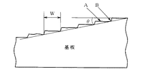
更に好ましい異種基板としては、(0001)面[C面]を主面とするサファイア、(112−0)面[A面]を主面とするサファイア、又は(111)面を主面とするスピネルである。ここで異種基板が、(0001)面[C面]を主面とするサファイアであるとき、前記薄膜の窒化物半導体25等に形成される保護膜や凹凸のストライプ形状が、そのサファイアの(112−0)面[A面]に対して垂直なストライプ形状を有していること[窒化物半導体の(101−0)[M面]に平行方向にストライプを形成すること]が好ましく、また、オフアングルのオフ角θ(図8に示すθ)は好ましくは0.1°〜0.5°、より好ましくは0.1°〜0.2°である。
【0073】
また(112−0)面[A面]を主面とするサファイアであるとき、前記保護膜や凹凸のストライプ形状はそのサファイアの(11−02)面[R面]に対して垂直なストライプ形状を有していることが好ましく、また(111)面を主面とするスピネルであるとき、前記凹凸のストライプ形状はそのスピネルの(110)面に対して垂直なストライプ形状を有していることが好ましい。
ここでは、保護膜や凹凸がストライプ形状の場合について記載したが、本発明においてサファイアのA面及びR面、スピネルの(110)面に窒化物半導体が横方向に成長し易いので、これらの面に第4の窒化物半導体の端面が形成されるように保護膜や凹凸の形成を考慮することが好ましい。
【0074】
本発明において用いられる異種基板21について図を用いて更に詳細に説明する。図6はサファイアの結晶構造を示すユニットセル図である。
まず、C面を主面とするサファイアを用い、凹凸はサファイアA面に対して垂直なストライプ形状とする場合について説明する。例えば、図7は主面側のサファイア基板の平面図である。この図はサファイアC面を主面とし、オリエンテーションフラット(オリフラ)面をA面としている。この図に示すように保護膜や凹凸のストライプをA面に対して垂直方向で、互いに平行なストライプを形成する。図7に示すように、サファイアC面上に窒化物半導体を選択成長させた場合、窒化物半導体は面内ではA面に対して平行な方向で成長しやすく、垂直な方向では成長しにくい傾向にある。従ってA面に対して垂直な方向でストライプを設けると、ストライプとストライプの間の窒化物半導体がつながって成長しやすくなり、ELOG成長が容易に可能となると考えられるが詳細は定かではない。
【0075】
次に、A面を主面とするサファイア基板を用いた場合、上記C面を主面とする場合と同様に、例えばオリフラ面をR面とすると、R面に対して垂直方向に、互いに平行なストライプを形成することにより、ストライプ幅方向に対して窒化物半導体が成長しやすい傾向にあるため、転位の少ない窒化物半導体層を成長させることができる。
【0076】
また次に、スピネル(MgAl2O4)に対しても、窒化物半導体の成長は異方性があり、窒化物半導体の成長面を(111)面とし、オリフラ面を(110)面とすると、窒化物半導体は(110)面に対して平行方向に成長しやすい傾向がある。従って、(110)面に対して垂直方向にストライプを形成すると窒化物半導体層と隣接する窒化物半導体同士が保護膜の上部でつながって、転位の少ない結晶を成長できる。なおスピネルは四方晶であるため特に図示していない。
【0077】
次に、本発明の成長方法において、図3に示すように、第2の工程では、上記第1の工程のELOG成長により形成された第1の窒化物半導体22上に、成長速度を500μm/時間以下10μm/時間以上で、第3の窒化物半導体23を成長させる。
第2の工程で、第3の窒化物半導体23を成長させる成長速度は、上記のように500μm/時間以下10μm/時間以上、好ましくは100μm/時間以下50μm/時間以上である。第3の窒化物半導体23を成長させる速度が、上記範囲であると、第3の窒化物半導体23を上記の膜厚に成長させる際に、異常成長が防止でき、更に第3の窒化物半導体23の成長面がきれいとなり好ましい。例えば成長速度が上記範囲となる具体的な方法としては、例えばHVPE等が挙げられる。
【0078】
第2の工程で成長される第3の窒化物半導体23としては、特に限定されないが、GaNからなる窒化物半導体が結晶性の点などから好ましい。また、第3の窒化物半導体23は、アンドープでも不純物をドープされてもよいが、アンドープであると結晶性の点で好ましい。
【0079】
第3の窒化物半導体23の膜厚は、前記第1の窒化物半導体22の膜厚より厚く成長される。第3の窒化物半導体23の膜厚としては、特に限定されないが、後述の第3の工程で少なくとも異種基板21を除去された後、第5の工程を行う際やデバイス構造を形成する際等の物理的強度に耐えられ、欠けや割れ等の生じにくい膜厚以上で、装置の大きさや操作がし易い範囲の膜厚が望ましい。
例えば、第3の窒化物半導体23の具体的な膜厚としては、好ましくは50μm〜1000μm、より好ましくは80μm〜500μmである。このような範囲の膜厚であると、第3の窒化物半導体23を窒化物半導体基板1とした場合に、操作性よく、また欠けや割れ等の発生が防止でき好ましい。
【0080】
次に、図4に示すように、第3の工程では、第2の工程で第3の窒化物半導体23を成長後に、少なくとも異種基板21を除去して、少なくとも第3の窒化物半導体23を有する第5の工程で用いられる窒化物半導体基板1とする。第3の工程で除去される部分としては、少なくとも異種基板21が除去されていればよく、図2のバッファ層、薄膜の窒化物半導体25、又は第1の保護膜13等を有していても、劈開により共振面を形成できる。好ましくは異種基板21〜第1の窒化物半導体22までが除去されていると、第3の窒化物半導体23の反りの軽減の点で好ましく、更に保護膜上の空隙の発生の可能性のある第1の窒化物半導体22を除去すると劈開性がより良好となる。
また、第3の工程で除去される部分は、製造工程での操作性のし易さや、反り等を考慮して、第3の窒化物半導体の一部までを除去してもよい。
第3の窒化物半導体23から異種基板21等を除去する方法としては、例えば研磨等の方法が挙げられる。
また、第3の窒化物半導体23を第5の工程での窒化物半導体基板1とする場合、第3の窒化物半導体23の異種基板21等を除去した面とは反対の面上に第5の工程のELOG成長を行う。
【0081】
次に、第4の工程を有する場合について説明する。
図5に示すように、上記第3の工程後に、第4の工程において、第3の窒化物半導体23の異種基板21等を除去した面とは反対の面上に、成長速度を500μm/時間以下10μm/時間以上で、第2の窒化物半導体を成長させる。第4の工程を有する場合は、第5の工程での窒化物半導体基板1は、少なくとも第3の窒化物半導体と第2の窒化物半導体とからなり、好ましくは第3と第2の窒化物半導体のみからなる。
【0082】
また、本発明の成長方法において、第4の工程を有する場合、第2の窒化物半導体24を成長後に第3の窒化物半導体を除去し、第5の工程で用いられる窒化物半導体基板1として、第2の窒化物半導体24のみからなるものを用いてもよい。第4の工程後に、第3の窒化物半導体23を除去して、第2の窒化物半導体24のみにすると、第3と第2の窒化物半導体との境界部分が除去されるので、境界部分に生じると思われる酸化膜を除去でき素子特性(寿命特性等)の向上の点で好ましい。第2の窒化物半導体のみを第5の工程で用いる窒化物半導体基板1とする場合、第2の窒化物半導体の膜厚は、特に限定されないが、例えば80〜500μmの膜厚を有することが物理的強度の点で好ましい。
【0083】
第2の窒化物半導体24としては、特に限定されないが、上記第3の窒化物半導体23と同様の窒化物半導体を挙げることができる。
第2の窒化物半導体の成長速度は、上記のように500μm/時間以下10μm/時間以上であり、好ましくは上記第3の窒化物半導体23を成長させる場合と同様である。
このように異種基板21を除去した後で、第3の窒化物半導体23の成長面に第2の窒化物半導体24を成長させると、第3の窒化物半導体23の反りが軽減され、第5の工程やデバイス工程等を良好に行える。また、第2の窒化物半導体24を成長させるとより結晶性が向上し、第2の窒化物半導体24上に上記第5の工程を行うと、第4の窒化物半導体2の転位の低減及び結晶性の向上の点で好ましい。
【0084】
第2の窒化物半導体24の膜厚は、特に限定されず、第2の窒化物半導体24の膜厚が厚いほど反りが軽減され結晶性の向上の点で好ましいが、あまり厚膜にすると操作性等が低下する場合や装置の大きさに限りがあるので、第3の窒化物半導体23と第2の窒化物半導体24の膜厚の合計が1000μm以下、好ましくは800μm以下、好ましくは400μm以下となることが好ましく、少なくとも第3と第2の窒化物半導体の膜厚が共に80μm以上であることが好ましい。膜厚がこの範囲であると物理的強度及び操作性等の点で好ましい。この場合、第3の窒化物半導体23の膜厚は、上記の膜厚の範囲で且つ第3と第2の窒化物半導体の膜厚の合計が1000μm以下となるように調整される。
【0085】
次に、上記本発明の窒化物半導体の成長方法により得られる本発明の基板上に、デバイス構造を形成してなる窒化物半導体素子について説明する。
本発明の窒化物半導体素子は、上記本発明の方法により得られる窒化物半導体の基板上(窒化物半導体基板1上に成長された第4の窒化物半導体2上)に、少なくともn型窒化物半導体、活性層、及びp型窒化物半導体を有するデバイス構造が形成されてなる素子が挙げられる。
上記素子を構成するn型窒化物半導体などは、特に限定されず、従来公知のデバイス構造を適宜用いることができる。デバイス構造の一実施の形態としては、後述の実施例に示されるものが挙げられる。しかし、本発明はこれに限定されない。また、電極や素子の形状なども特に限定されず、公知の種々のものを用いることができる。
つまり、前記本発明の窒化物半導体の成長方法により得られる基板が転位の低減された良好な基板であるので、デバイス構造の種類により差あるものの、寿命特性を良好にすることができるものである。また、基板は窒化物半導体からなるので窒化物半導体のM軸方向に垂直な面で良好に劈開できる。
【0086】
また本発明において、好ましい窒化物半導体素子としては、例えばレーザ素子において、発光領域がリッジ形状のストライプであるのもが寿命特性などの素子特性の点から挙げられる。
より好ましい素子としては、リッジ形状のストライプが、上記第5の工程で形成されるストライプ形状の第2の保護膜11及び第2の凹凸13のストライプ方向に平行に形成され、さらに好ましくはストライプ形状の第2の保護膜11の保護膜上部及び第2の凹凸13の凹部上部に形成されることが寿命特性を向上させる点で好ましい。
第5の工程のELOG成長の種類によって、第4の窒化物半導体2表面の平均の転位密度に差はあるが、第2の保護膜11上部及び第2の凹凸13の凹部上部には転位がほとんど見られなくなることから、この部分に発光領域、例えば上記のようなリッジ形状のストライプを形成すると、レーザ素子などを作動中に転位の伝播を防止でき素子劣化を抑制し寿命特性の向上が可能となる。
【0087】
【実施例】
以下に本発明の一実施の形態である実施例を示し、更に本発明を詳細に説明する。しかし本発明はこれに限定されない。
【0088】
[実施例1]
以下に図1(a)に示される窒化物半導体基板1と第4の窒化物半導体2からなる窒化物半導体の基板を製造させる工程を示す。(第1の工程から第3の工程は図2〜図4を参照)
【0089】
[窒化物半導体基板1の製造]
(第1の工程)
異種基板21として、C面を主面とし、オリフラ面をA面とするサファイア基板21を用い、このサファイア基板21をMOCVDの反応容器内にセットし、温度を510℃にして、キャリアガスに水素、原料ガスにアンモニアとTMG(トリメチルガリウム)とを用い、サファイア基板21上にGaNよりなるバッファ層を200オングストロームの膜厚で成長させる。
【0090】
バッファ層成長後、TMGのみ止めて、温度を1050℃まで上昇させ、1050℃になったら、原料ガスにTMG、アンモニア、シランガスを用い、アンドープGaNよりなる薄膜の窒化物半導体25を5μmの膜厚で成長させる。
バッファ層と薄膜の窒化物半導体25とを積層したウェーハの、その薄膜の窒化物半導体25の上にストライプ状のフォトマスクを形成し、CVD装置によりストライプ幅18μm、窓部2μmのSiO2よりなる第1の保護膜12を0.5μmの膜厚で形成する。なお、第1の保護膜12のストライプ方向はサファイアA面に対して垂直な方向、つまり図7に示すように、オリフラ面に対して垂直な方向でとする。このように形成すると、サファイアのA面に垂直な方向が、窒化物半導体のM軸方向に対して平行方向となる。
【0091】
第1の保護膜12を形成後、ウェーハをMOCVDの反応容器に移し、1050℃にて、原料ガスにTMG、アンモニア、シランガス、Cp2Mg(シクロペンタジエニルマグネシウム)を用い、SiとMgの不純物を5×10¹⁷/cm3ドープしたGaNよりなる第1の窒化物半導体22をMOCVD装置により15μmの膜厚で成長させる。SiとMgの不純物は第1の窒化物半導体22の成長と同時にドープされる。但し、第1の窒化物半導体22の成長速度は、3μm/時間とした。
【0092】
得られた第1の窒化物半導体22の表面をCL(カソードルミネッセンス)により観察すると、第1の保護膜12上部はほとんど結晶欠陥が見られず、窓部上部は8×10⁵個/cm2程度観測された。転位密度は、観測される部分によりやや差が生じる場合がある。
【0093】
(第2の工程)
次に、第1の窒化物半導体22上に、アンドープのGaNからなる第3の窒化物半導体23をHVPE装置により200μmの膜厚で成長させる。但し、第3の窒化物半導体23の成長速度は、50μm/時間とした。
【0094】
(第3の工程)
次に、第3の窒化物半導体23を成長後に、サファイア基板21から第1の窒化物半導体22までを研磨により除去して第3の窒化物半導体24のみの窒化物半導体基板1が得られる。
得られた第3の窒化物半導体24のサファイア基板などを除去した面には、ストライプ状に転位のほとんどない部分とやや転位の多い部分とが存在している。一方、第3の窒化物半導体24の成長面は、平均的に転位密度が1×10⁷個/cm2程度存在している。
【0095】
[本発明の基板の製造]
(第5の工程)
上記の第3の窒化物半導体23からなる窒化物半導体基板1上に、第3の窒化物半導体23の除去面のストライプ状の転位分布と平行となるような窒化物半導体のM軸方向に対して平行方向に、第2の保護膜11を第3の窒化物半導体23の成長面(除去面とは反対の面)に、上記第1の工程で形成した第1の保護膜12と同様に形成する。
第2の保護膜11を形成後、第4の窒化物半導体2をMOCVD装置で15μmの膜厚で成長させる。
第4の窒化物半導体2の表面の転位密度は、窓部上部の表面にはわずかな転位が見られるが、第2の保護膜11上部の第4の窒化物半導体2の表面にはほとんど転位が見られない。
【0096】
[実施例2]
実施例1において、第2の工程で成長される第3の窒化物半導体23の膜厚を150μmとし、更に第3の工程後に下記第4の工程を追加する他は同様にしてデバイス構造を形成するための基板を製造する。
(第4の工程)
サファイア基板等を除去された第3の窒化物半導体23の成長面上に、アンドープのGaNからなる第2の窒化物半導体24を、HVPE装置により、200μmの膜厚で成長させる(図5)。
【0097】
得られた第3の窒化物半導体23と第2の窒化物半導体24からなる窒化物半導体基板1上に第5の工程のELOG成長をさせる。第3の窒化物半導体23の成長面に第2の窒化物半導体24を成長させると反りが軽減され、第5の工程でのELOG成長が実施例1より良好となり、転位の良好に低減された第4の窒化物半導体2を得ることができる。
【0098】
[実施例3]
以下に図1(b)に示される窒化物半導体基板1と第4の窒化物半導体2からなる窒化物半導体の基板を製造させる工程を示す。(第1の工程から第4の工程は図2〜図5を参照)
【0099】
(第1の工程)
異種基板21として、2インチφ、C面を主面とし、オリフラ面をA面とするサファイア基板21をMOCVDの反応容器内にセットし、温度を510℃にして、キャリアガスに水素、原料ガスにアンモニアとTMG(トリメチルガリウム)とを用い、サファイア基板21上にGaNよりなるバッファ層(図示されていない)を約200オングストロームの膜厚で成長させる。
【0100】
バッファ層を成長後、TMGのみ止めて、温度を1050℃まで上昇させる。1050℃になったら、原料ガスにTMG、アンモニアを用い、アンドープのGaNよりなる薄膜の窒化物半導体25を2μmの膜厚で成長させる。
【0101】
薄膜の窒化物半導体25を成長後、ストライプ状のフォトマスクを形成し、スパッタ装置によりストライプ幅15μm、ストライプ間隔(凹部の開口部)3μmのSiO2よりなる第1の保護膜12を0.5μmの膜厚で形成し、続いて、RIE装置により薄膜の窒化物半導体25の途中までエッチングして凹凸を形成することにより薄膜の窒化物半導体25の凹部側面を露出させる。なお、ストライプ方向は、図7に示すように、オリフラ面に対して垂直な方向で形成する。このようにオリフラ面に垂直な方向で成長させると、オリフラ面に垂直な方向が窒化物半導体のM軸方向に対して平行方向となる。
【0102】
薄膜の窒化物半導体25に、凹凸を形成した後、凹凸を形成した薄膜の窒化物半導体25の表面にスパッタ装置により保護膜材料を形成し、CF4とO2ガスにより、凹凸を形成したことにより形成された第1の窒化物半導体22の凹部側面の保護膜をエッチングにより除去して凹部側面を露出させ、凸部上部及び凹部底部に第1の保護膜12を形成する。
【0103】
第1の保護膜12を形成後、MOCVDの反応容器内にセットし、温度を1050℃で、原料ガスにTMG、アンモニア、シランガス、Cp2Mgを用い、成長と同時にSiとMgの不純物を5×10¹⁷/cm3ドープしたGaNよりなる第1の窒化物半導体22をMOCVD装置により15μmの膜厚で成長させる。但し、第1の窒化物半導体22の成長速度は、2μm/時間として行った。
【0104】
得られた第1の窒化物半導体22の表面をCL(カソードルミネッセンス)により観察すると、転位は非常に低減されている。但し、第1の窒化物半導体22の表面には、第1の保護膜12のストライプ方向と平行に転位の分布がわずかに見られる。この転位の分布は、他のほとんど転位の見られない部分とを相対的に比較した場合である。
【0105】
(第2の工程)
次に、第1の窒化物半導体22上に、アンドープのGaNからなる第3の窒化物半導体23をHVPE装置により100μmの膜厚で成長させる。但し、第3の窒化物半導体23の成長速度は、50μm/時間とした。
【0106】
(第3の工程)
次に、第3の窒化物半導体23を成長後に、サファイア基板21から第1の窒化物半導体22までを研磨により除去して第3の窒化物半導体23のみとする。第3の窒化物半導体23の除去面には、第1の窒化物半導体23の表面にわずかに分布していた転位分布とほぼ同様のものが見られる。
【0107】
(第4の工程)
次に、第3の窒化物半導体23の成長面上に、アンドープのGaNからなる第2の窒化物半導体24を、HVPE装置により、250μmの膜厚で成長させる。
得られた第3の窒化物半導体23と第2の窒化物半導体24からなる窒化物半導体基板[図2(b)]の表面には、わずかな転位がほぼ均一に見られる。
【0108】
(第5の工程)
上記の第3の窒化物半導体23と第2の窒化物半導体24からなる窒化物半導体基板1上に、第3の窒化物半導体23の除去面のストライプ状の非常にわずかな転位分布と平行となるような窒化物半導体のM軸方向に対して平行方向に、第2の保護膜11を第2の窒化物半導体24の成長面に、上記第1の工程で形成したように、凹凸を形成後に第1の保護膜12を形成したのと同様に、凹部底部と凸部上部に第2の保護膜11を形成する。
第2の保護膜11を形成後、第4の窒化物半導体2をMOCVD装置で15μmの膜厚で成長させる。
第4の窒化物半導体2の表面の転位は、全体的にほとんど見られない。そして、窒化物半導体基板1と第4の窒化物半導体2からなる基板1[図1(b)]は、転位がほとんど見られず、欠けや割れが発生しにくい。
【0109】
[実施例4]
以下に図1(c)の基板を製造する方法について記載する。
(第1の工程)
異種基板1として、2インチφ、C面を主面とし、オリフラ面をA面とするサファイア基板1を反応容器内にセットし、温度を510℃にして、キャリアガスに水素、原料ガスにアンモニアとTMG(トリメチルガリウム)とを用い、サファイア基板1上にGaNよりなるバッファ層(図示されていない)を約200オングストロームの膜厚で成長させる。
【0110】
バッファ層を成長後、TMGのみ止めて、温度を1050℃まで上昇させる。1050℃になったら、原料ガスにTMG、アンモニアを用い、アンドープのGaNよりなる薄膜の窒化物半導体25を2μmの膜厚で成長させる。
【0111】
薄膜の窒化物半導体25を成長後、ストライプ状のフォトマスクを形成し、スパッタ装置によりストライプ幅15μm、ストライプ間隔(凹部の開口部)2μmのSiO2よりなる第1の保護膜11を0.5μmの膜厚で形成し、続いて、RIE装置によりサファイア基板1が露出するまで薄膜の窒化物半導体25をエッチングして凹凸を形成することにより薄膜の窒化物半導体25の凹部側面を露出させることにより凸部上部のみに第1の保護膜12を形成する。凹部側面の幅dはほぼ2μmである。なお、ストライプ方向は、図7に示すように、オリフラ面に対して垂直な方向であり、窒化物半導体のM軸方向に対して平行方向となる。
【0112】
第1の保護膜12を形成後、反応容器内にセットし、温度を1050℃で、原料ガスにTMG、アンモニア、シランガス、Cp2Mgを用い、成長と同時にSiとMgの不純物を5×10¹⁷/cm3ドープしたGaNよりなる第1の窒化物半導体22を、MOCVD装置により、15μmの膜厚で成長させる。第1の窒化物半導体22の成長速度は、2μm/時間である。
【0113】
(第2の工程)
次に第1の窒化物半導体22上に、アンドープのGaNからなる第3の窒化物半導体23を、HVPE装置により、150μmの膜厚に成長させる。成長速度は、50μm/時間である。
【0114】
(第3の工程)
第3の窒化物半導体23を成長後、サファイア基板から第1の窒化物半導体22までを除去し、第3の窒化物半導体23のみとする。第3の窒化物半導体23の除去面には、わずかな転位が第1の保護膜12と平行にストライプ状に分布している。
【0115】
(第4の工程)
第3の窒化物半導体23の成長面上に、アンドープのGaNからなる第2の窒化物半導体24を、HVPE装置により、200μmの膜厚に成長させる。成長速度は、50μm/時間である。
以上の工程を経ることにより、第3の窒化物半導体23と第2の窒化物半導体24からなる窒化物半導体基板1[図2(c)]を得ることができる。得られた窒化物半導体基板1の表面には1×10⁷個/cm2程度の転位が見られる。
【0116】
(第5の工程)
次に、上記の第3の窒化物半導体23と第2の窒化物半導体24からなる窒化物半導体基板1の表面に、ストライプ状のフォトマスクを形成し、スパッタ装置によりストライプ幅15μm、ストライプ間隔(凹部の開口部の幅w)2μmのSiO2よりなる第2の保護膜11を0.5μmの膜厚で形成し、続いて、RIE装置により凹部側面の幅dがほぼ2μmの深さにエッチングして凹凸を形成することにより、凸部上部にのみ第2の保護膜11を形成する。形成された第2の保護膜11のストライプ方向は、第1の保護膜12のストライプ方向と平行となるように、窒化物半導体基板1の3種あるM軸方向のうち同一のM軸方向に対して平行方向である。
【0117】
上記のように凸部上部のみに第2の保護膜11を形成した後、第4の窒化物半導体2を、30μmの膜厚で成長させる。
第4の窒化物半導体2の表面の転位は、窓部上部の表面にわずかにストライプ状に分布しているが、全体的に転位が非常に低減された窒化物半導体基板1と第4の窒化物半導体2からなる基板[図1(c)]を得ることができる。
【0118】
[実施例5]
以下に、図1(d)に示される基板を製造する方法についての一実施の形態である。(第1の工程から第4の工程は図2(d)〜図5を参照)
(第1の工程)
異種基板21として、2インチφ、C面を主面とし、オリフラ面をA面とするサファイア基板21を反応容器内にセットし、温度を510℃にして、キャリアガスに水素、原料ガスにアンモニアとTMG(トリメチルガリウム)とを用い、サファイア基板21上にGaNよりなるバッファ層(図示されていない)を約200オングストロームの膜厚で成長させる。
【0119】
バッファ層を成長後、TMGのみ止めて、温度を1050℃まで上昇させる。1050℃になったら、原料ガスにTMG、アンモニア、シランガスを用い、Siを1×10¹⁸/cm3ドープしたGaNよりなる薄膜の窒化物半導体層25を2μmの膜厚で成長させる。
【0120】
薄膜の窒化物半導体層25を成長後、ストライプ状のフォトマスクを形成し、スパッタ装置によりストライプ幅(凸部の上部になる部)5μm、ストライプ間隔(凹部底部となる部分)10μmにパターニングされたSiO2膜を形成し、続いて、RIE装置によりSiO2膜の形成されていない部分の薄膜の窒化物半導体層25を薄膜の窒化物半導体25が残る程度に途中までエッチングして凹凸を形成することにより、凹部側面に薄膜の窒化物半導体25を露出させる。凹凸を形成した後、凸部上部のSiO2を除去することにより第1の凹凸14を形成する。なお、第1の凹凸14のストライプ方向は、図7に示すように、オリフラ面に対して垂直な方向で形成する。
【0121】
次に、反応容器内にセットし、温度を1050℃で、原料ガスにTMG、アンモニア、シランガスを用い、アンドープのGaNよりなる第1の窒化物半導体層22を、MOCVD装置により、15μmの膜厚で成長させる。成長速度は、2μm/時間である。
【0122】
(第2の工程)
上記第1の窒化物半導体22上に、アンドープのGaNからなる第3の窒化物半導体23を、HVPE装置により、100μmの膜厚で成長させる。成長速度は、50μm/時間である。
【0123】
(第3の工程)
第3の窒化物半導体23を成長後に、サファイア基板1から第1の窒化物半導体までを除去して、単独の第3の窒化物半導体23とする。
【0124】
(第4の工程)
第3の工程で得られた第3の窒化物半導体23の成長面上に、アンドープのGaNからなる第2の窒化物半導体24を、HVPE装置により、200μmの膜厚で成長させる。成長速度は、50μm/時間である。
【0125】
上記の工程を経ることにより、第3の窒化物半導体23と第2の窒化物半導体24からなる窒化物半導体基板が得られる。得られた第2の窒化物半導体24表面には、5×10⁶個/cm2程度の転位が見られた。また、第3の窒化物半導体23の除去面には転位の分布が、凹部開口部から成長した部分にはほとんど転位が見られないが、凸部上部から成長した部分には1×107個/cm2程度の転位が第1の凹凸13のストライプ方向に平行に分布している。
【0126】
(第5の工程)
次に、図1(c)の基板を成長させる。
上記の第3の窒化物半導体23と第2の窒化物半導体24からなる窒化物半導体基板1上に、上記第1の工程で形成した第1の凹凸14と同様に、第2の凹凸13を形成する。但し、第2の凹凸13のストライプ方向は、第1の凹凸14のストライプ方向と平行となるように、上記第3の窒化物半導体23の除去面に分布しているストライプ状の転位と平行となるように形成することで、窒化物半導体のM軸方向に対して平行方向となる。この第2の凹凸13を有する上にアンドープのGaNからなる第4の窒化物半導体2を20μmの膜厚で成長させる。
得られた窒化物半導体基板1と第4の窒化物半導体2とからなる基板の表面は、凹部開口部から成長した部分には転位がほとんど見られず、凸部上部から成長した部分には転位がわずかに見られる程度である。また基板は欠け等の防止される程度の膜厚を有している。
【0127】
[実施例6]
実施例5において、第4の工程で第2の窒化物半導体24を300μmの膜厚で成長させ、その後第3の窒化物半導体23を研磨して除去し、ほぼ250μmの膜厚の第2の窒化物半導体24を第5の工程で用いられる窒化物半導体基板1とする他は同様にして本発明の基板を製造する。
得られた本発明の基板は、実施例5と同様に、転位が低減され、特に凹部上部の表面には、転位がほとんど見られない。
【0128】
以下に、上記本発明の窒化物半導体の成長方法により得られた本発明の基板を用いてなる、本発明の窒化物半導体素子の一実施の形態である窒化物半導体素子の実施例を示す。しかし本発明はこれに限定されない。
[実施例7]
実施例1により得られた第3の窒化物半導体23からなる窒化物半導体の基板上に第4の窒化物半導体2を成長させてなる基板上に、以下のデバイス構造を順に成長させる。
【0129】
(アンドープn型コンタクト層)[図9には図示されていない]
窒化物半導体の基板上に、1050℃で原料ガスにTMA(トリメチルアルミニウム)、TMG、アンモニアガスを用いアンドープのAl0.05Ga0.95Nよりなるn型コンタクト層を1μmの膜厚で成長させる。
(n型コンタクト層72)
次に、同様の温度で、原料ガスにTMA、TMG及びアンモニアガスを用い、不純物ガスにシランガス(SiH4)を用い、Siを3×10¹⁸/cm3ドープしたAl0.05Ga0.95Nよりなるn型コンタクト層72を3μmの膜厚で成長させる。
【0130】
(クラック防止層73)
次に、温度を800℃にして、原料ガスにTMG、TMI(トリメチルインジウム)及びアンモニアを用い、不純物ガスにシランガスを用い、Siを5×10¹⁸/cm3ドープしたIn0.08Ga0.92Nよりなるクラック防止層73を0.15μmの膜厚で成長させる。
【0131】
(n型クラッド層74)
次に、温度を1050℃にして、原料ガスにTMA、TMG及びアンモニアを用い、アンドープのAl0.14Ga0.86NよりなるA層を25オングストロームの膜厚で成長させ、続いて、TMAを止め、不純物ガスとしてシランガスを用い、Siを5×10¹⁸/cm3ドープしたGaNよりなるB層を25オングストロームの膜厚で成長させる。そして、この操作をそれぞれ160回繰り返してA層とB層の積層し、総膜厚8000オングストロームの多層膜(超格子構造)よりなるn型クラッド層74を成長させる。
【0132】
(n型ガイド層75)
次に、同様の温度で、原料ガスにTMG及びアンモニアを用い、アンドープのGaNよりなるn型ガイド層75を0.075μmの膜厚で成長させる。
【0133】
(活性層76)
次に、温度を800℃にして、原料ガスにTMI、TMG及びアンモニアを用い、不純物ガスとしてシランガスを用い、Siを5×10¹⁸/cm3ドープしたIn0.01Ga0.99Nよりなる障壁層を100オングストロームの膜厚で成長させる。続いて、シランガスを止め、アンドープのIn0.11Ga0.89Nよりなる井戸層を50オングストロームの膜厚で成長させる。この操作を3回繰り返し、最後に障壁層を積層した総膜厚550オングストロームの多重量子井戸構造(MQW)の活性層76を成長させる。
【0134】
(p型電子閉じ込め層77)
次に、同様の温度で、原料ガスにTMA、TMG及びアンモニアを用い、不純物ガスとしてCp2Mg(シクロペンタジエニルマグネシウム)を用い、Mgを1×10¹⁹/cm3ドープしたAl0.4Ga0.6Nよりなるp型電子閉じ込め層77を100オングストロームの膜厚で成長させる。
【0135】
(p型ガイド層78)
次に、温度を1050℃にして、原料ガスにTMG及びアンモニアを用い、アンドープのGaNよりなるp型ガイド層78を0.075μmの膜厚で成長させる。
このp型ガイド層78は、アンドープとして成長させるが、p型電子閉じ込め層77からのMgの拡散により、Mg濃度が5×10¹⁶/cm3となりp型を示す。
【0136】
(p型クラッド層79)
次に、同様の温度で、原料ガスにTMA、TMG及びアンモニアを用い、アンドープのAl0.1Ga0.9NよりなるA層を25オングストロームの膜厚で成長させ、続いて、TMAを止め、不純物ガスとしてCp2Mgを用い、Mgを5×10¹⁸/cm3ドープしたGaNよりなるB層を25オングストロームの膜厚で成長させる。そして、この操作をそれぞれ100回繰り返してA層とB層の積層し、総膜厚5000オングストロームの多層膜(超格子構造)よりなるp型クラッド層79を成長させる。
【0137】
(p型コンタクト層80)
次に、同様の温度で、原料ガスにTMG及びアンモニアを用い、不純物ガスとしてCp2Mgを用い、Mgを1×10²⁰/cm3ドープしたGaNよりなるp型コンタクト層80を150オングストロームの膜厚で成長させる。
【0138】
反応終了後、反応容器内において、ウエハを窒素雰囲気中、700℃でアニーリングを行い、p型層を更に低抵抗化する。
アニーリング後、ウエハを反応容器から取り出し、最上層のp側コンタクト層の表面にSiO2よりなる保護膜を形成して、RIE(反応性イオンエッチング)を用いSiCl4ガスによりエッチングし、図10に示すように、n電極を形成すべきn側コンタクト層2の表面を露出させる。
次に図10(a)に示すように、最上層のp側コンタクト層80のほぼ全面に、PVD装置により、Si酸化物(主として、SiO2)よりなる第2の保護膜61を0.5μmの膜厚で形成した後、第2の保護膜61の上に所定の形状のマスクをかけ、フォトレジストよりなる第3の保護膜63を、ストライプ幅1.8μm、厚さ1μmで形成する。
次に、図10(b)に示すように第3の保護膜63形成後、RIE(反応性イオンエッチング)装置により、CF4ガスを用い、第3の保護膜63をマスクとして、前記第2の保護膜をエッチングして、ストライプ状とする。その後エッチング液で処理してフォトレジストのみを除去することにより、図10(c)に示すようにp側コンタクト層80の上にストライプ幅1.8μmの第2の保護膜61が形成できる。
【0139】
さらに、図10(d)に示すように、ストライプ状の第2の保護膜61形成後、再度RIEによりSiCl4ガスを用いて、p側コンタクト層10、およびp側クラッド層89をエッチングして、ストライプ幅1.8μmのリッジ形状のストライプを形成する。但し、リッジ形状のストライプは、図9に示すように、ELOG成長を行う際に形成した第2の保護膜11の上部で且つ第2の保護膜11の中心部分を避けるように形成される。
リッジストライプ形成後、ウェーハをPVD装置に移送し、図10(e)に示すように、Zr酸化物(主としてZrO2)よりなる第1の保護膜62を、第2の保護膜61の上と、エッチングにより露出されたp側クラッド層79の上に0.5μmの膜厚で連続して形成する。このようにZr酸化物を形成すると、p−n面の絶縁をとるためと、横モードの安定を図ることができ好ましい。
次に、ウェーハをフッ酸に浸漬し、図10(f)に示すように、第2の保護膜61をリフトオフ法により除去する。
【0140】
次に図10(g)に示すように、p側コンタクト層80の上の第2の保護膜61が除去されて露出したそのp側コンタクト層の表面にNi/Auよりなるp電極20を形成する。但しp電極20は100μmのストライプ幅として、この図に示すように、第1の保護膜62の上に渡って形成する。
第1の保護膜62形成後、図9に示されるように露出させたn側コンタクト層72の表面にはTi/Alよりなるn電極21をストライプと平行な方向で形成する。
【0141】
以上のようにして、n電極とp電極とを形成したウェーハを、ストライプ状の電極に垂直な方向で、基板側からバー状に劈開し、劈開面(11−00面、六角柱状の結晶の側面に相当する面=M面)に共振器を作製する。共振器面にSiO2とTiO2よりなる誘電体多層膜を形成し、最後にp電極に平行な方向で、バーを切断して図9に示すようなレーザ素子とする。
得られたレーザ素子をヒートシンクに設置し、それぞれの電極をワイヤーボンディングして、室温でレーザ発振を試みた。
その結果、室温においてしきい値2.5kA/cm2、しきい値電圧5Vで、発振波長400nmの連続発振が確認され、室温で1万時間以上の寿命を示す。更に、デバイス構造の形成時や共振面を劈開により形成する際等に欠けや割れが防止され、良好な共振面が得られ更に歩留まりが向上する。
【0142】
[実施例8]
実施例7において、窒化物半導体の基板として、実施例2〜実施例6の基板をそれぞれ用いる他は同様にして、レーザ素子を作製した。得られた5種のレーザ素子は、実施例7とほぼ同様に、デバイス構造を形成するための基板の表面には転位が非常に低減され、更には転位のほとんど見られない部分を有しているので、寿命特性が良好であり、デバイス構造の形成時や共振面を劈開により形成する時等に欠けや割れが防止され良好な結果を得ることができる。
【0143】
【発明の効果】
本発明は、窒化物半導体を基板としてデバイス構造を形成したり、劈開により共振面を形成しても、基板に欠けやクラックの発生が生じず、更に窒化物半導体の基板の表面部分の転位を低減し、特に成長面の表面にほとんど転位のない部分を有しており、寿命特性等の素子特性を良好にすることができ、実用化に際しての信頼性の向上が達成できるような窒化物半導体からなる基板の得られる窒化物半導体の成長方法を提供することができる。
更に、本発明は、本発明の窒化物半導体の成長方法により得られる窒化物半導体を基板とし、寿命特性など素子特性の良好な窒化物半導体素子を提供することができる。
【図面の簡単な説明】
【図1】 図1は、本発明のデバイス構造を形成するための窒化物半導体の基板の一実施の形態である基板の模式的断面図である。
【図2】 図2は、本発明の第5の工程での窒化物半導体基板となる窒化物半導体を成長させる工程の一実施の形態であるウエハの模式的断面図である。
【図3】 図3は、本発明の第5の工程での窒化物半導体基板となる窒化物半導体を成長させる工程の一実施の形態であるウエハの模式的断面図である。
【図4】 図4は、本発明の第5の工程での窒化物半導体基板となる窒化物半導体を成長させる工程の一実施の形態であるウエハの模式的断面図である。
【図5】 図5は、本発明の第5の工程での窒化物半導体基板となる窒化物半導体を成長させる工程の一実施の形態であるウエハの模式的断面図である。
【図6】 図6は、サファイアの面方位を示すユニットセル図である。
【図7】 図7は、保護膜のストライプ方向を説明するための基板主面側の平面図である。
【図8】 図8は、オフアングルした異種基板の部分的な形状を示す模式的断面図である。
【図9】 図9は、本発明の一実施の形態である窒化物半導体レーザ素子を示す模式的断面図である。
【図10】 図10は、リッジ形状のストライプを形成する一実施の形態である方法の各工程におけるウエハの部分的な構造を示す模式的断面図である。
【符号の説明】
1・・・窒化物半導体基板
2・・・第4の窒化物半導体
11・・・第2の保護膜
12・・・第1の保護膜
13・・・第2の凹凸
14・・・第1の凹凸
21・・・異種基板
22・・・第1の窒化物半導体
23・・・第3の窒化物半導体
24・・・第2の窒化物半導体
25・・・薄膜の窒化物半導体[0001]
BACKGROUND OF THE INVENTION
The present invention relates to a nitride semiconductor (InXAlYGa1-XYN, 0 ≦ X, 0 ≦ Y, X + Y ≦ 1), and more particularly, to a nitride semiconductor growth method with few dislocations. The present invention also provides a nitride semiconductor (In) used in a light-emitting element such as a light-emitting diode or a laser diode, or a light-receiving element such as a solar cell or an optical sensor, using the substrate made of the nitride semiconductor.XAlYGa1-XYN, 0 ≦ X, 0 ≦ Y, X + Y ≦ 1).
[0002]
[Prior art]
In recent years, blue and blue-green light emitting diodes (LEDs) and laser diodes (LDs) made of nitride semiconductors have been put into practical use.
[0003]
For example, the present inventors have grown a film thickness of 2 μm on sapphire by metalorganic chemical vapor deposition (MOCVD) in Aplide Physics Letters. Vol. 73, Number 6 (1998) pp. 832-834. On the GaN layer, SiO film with a thickness of 0.1 μm2Then, GaN is again grown on the surface having the protective film to a thickness of 20 μm by MOCVD (ELOG growth), followed by 200 μm by hydride vapor phase epitaxy (HVPE). The sapphire substrate is removed by polishing to obtain a GaN substrate having a thickness of about 150 μm, and a device structure is formed on the GaN substrate. A nitride semiconductor device is reported which is formed by cleaving at a crystal side face; for example, {1-100} etc. to form a resonance face.
The reported laser element has a good far-field pattern of laser light from the resonance surface formed by cleavage, and the operating current is adjusted so that the output is 5 mW, and the condition is approximately 180 hours under the condition of 50 ° C. Continuous oscillation is possible.
[0004]
[Problems to be solved by the invention]
However, the nitride semiconductor device reported in the above Appl. Phys. Lett. Has the possibility of practical use of the laser device, but the life characteristics are not sufficiently satisfactory for practical use. . The laser element reported above can continuously oscillate at a high temperature for a considerably long time. However, if the continuous oscillation exceeds 180 hours, the operating current increases rapidly, so that the deterioration of the element has progressed considerably. I can guess.
[0005]
As a result of various studies for further improvement of the lifetime characteristics, the present inventors have found that the surface of the nitride semiconductor substrate on which the device structure is grown is almost uniformly 1 × according to observation with a surface transmission electron microscope (surface TEM). 107Piece / cm2A certain degree of dislocation was confirmed, and it was thought that this dislocation would reduce the life characteristics. The dislocation density is considerably reduced compared to the case where GaN is grown on a conventional sapphire substrate, but in order to ensure the reliability of the device in practical use, the life characteristics are further improved. There is a need.
[0006]
The reason why dislocations are found almost uniformly on the surface of the nitride semiconductor substrate is to grow the nitride semiconductor to a thickness of 200 μm with HVPE in order to improve the physical strength during cleavage and prevent chipping and cracking. In the process, it can be assumed that the dislocations seen in the upper part of the portion (window) where the protective film is not formed are uniformly spread with the growth of the nitride semiconductor.
[0007]
By the way, when a nitride semiconductor is grown to a thickness of 20 μm by MOCVD after forming the protective film, the upper portion of the window is almost 1 × 10⁹Piece / cm2On the other hand, almost no dislocation is observed on the upper part of the protective film. If a device structure, particularly a ridge-shaped stripe, is formed on the protective film without dislocations, the life characteristics are improved. However, in order to remove sapphire from a nitride semiconductor having a thickness of 20 μm and form a resonance surface by cleavage, the nitride semiconductor substrate having a thickness of 20 μm does not have sufficient physical strength, resulting in chipping and cracking. Yield decreases. Furthermore, the physical strength of the nitride semiconductor substrate is also required when forming the device structure.
Thus, removing sapphire and forming a device structure on a nitride semiconductor-only substrate enables a simple method of cleaving to obtain a mirror-like resonant surface, but at the time of cleavage and The film must be grown to such a thickness that the physical strength at the time of the device process is sufficient. For this reason, a portion having almost no dislocations obtained by the ELOG growth is lost from the surface of the nitride semiconductor substrate.
As described above, in order to improve the lifetime characteristics of the laser element, it is desired to further reduce the dislocation density of the nitride semiconductor substrate for forming the device structure.
[0008]
Therefore, the object of the present invention is that when a nitride semiconductor is used as a substrate, even if a device structure is formed or a resonance surface is formed by cleavage, no cracks or cracks are generated in the substrate. It is an object of the present invention to provide a nitride semiconductor growth method for obtaining a nitride semiconductor substrate in which dislocations are reduced so that the reliability of the device in practical use can be improved and the reliability of the device is improved.
Furthermore, an object of the present invention is to provide a nitride semiconductor device having good device characteristics such as life characteristics, using a nitride semiconductor obtained by the nitride semiconductor growth method of the present invention as a substrate.
[0009]
[Means for Solving the Problems]
That is, the object of the present invention can be achieved by the following configurations (1) to (13).
(1) On a heterogeneous substrate made of a material different from nitride semiconductorForming exposed irregularities on the grown nitride semiconductor; and,On the surface having the exposed unevenness, the upper surface of the uneven surface and the side surface of the recessed surfaceGrowing a first nitride semiconductor using lateral growth;afterwards,Removing at least the heterogeneous substrate to form a nitride semiconductor substrate; and growing a second nitride semiconductor on a surface of the nitride semiconductor substrate opposite to the surface from which the heterogeneous substrate has been removed; A method for growing a nitride semiconductor, comprising:
(2) The nitride semiconductor growth method according to (1), wherein the nitride semiconductor substrate has a warp.
(3The first nitride semiconductor is grown at a growth rate of 10 μm / hour or less and 0.5 μm / hour or more.The second nitride semiconductor is grown at a growth rate of 500 μm / hour or less and 10 μm / hour or more.(1)Or (2)4. A method for growing a nitride semiconductor according to 1.
(4) The first nitride semiconductor is grown by metal organic chemical vapor deposition, and the second nitride semiconductor is grown by hydride vapor deposition. (1) to (3) The method for growing a nitride semiconductor according to any one of the above.
(5) The first nitride semiconductor is grown by promoting lateral growth from the side surface of the concave portion as compared with vertical growth from the concave bottom portion of the concave and convex portions. The method for growing a nitride semiconductor according to any one of the above.
(6) Any one of (1) to (5), wherein growth from the side surface of the recess is bonded inside the recess to prevent growth from the bottom of the recess and to grow the first nitride semiconductor. A method for growing a nitride semiconductor according to
(7) The first nitride semiconductor is grown by promoting lateral growth by doping p-type impurities and / or n-type impurities. A method for growing a nitride semiconductor according to
(8) The method for growing a nitride semiconductor according to any one of (1) to (6), wherein the first and second nitride semiconductors are made of undoped GaN.
(9) The unevenness is parallel to the M-axis direction of the nitride semiconductor substrate and any one of <1-100>, <10-10>, and <01-10>. The method for growing a nitride semiconductor according to any one of (1) to (8), wherein the nitride semiconductor has a formed stripe shape.
(10And a step of growing a third nitride semiconductor on the first nitride semiconductor after the first nitride semiconductor is grown, wherein the nitride semiconductor substrate includes at least a third nitride. (1) to () characterized by comprising a semiconductor9The method for growing a nitride semiconductor according to any one of the above.
(11) In the step of removing the heterogeneous substrate, part of the third nitride semiconductor is removed from the heterogeneous substrate.(10)4. A method for growing a nitride semiconductor according to 1.
(12) The nitride semiconductor substrate has a dislocation density of 10 on the surface thereof.TenPiece / cm2The method for growing a nitride semiconductor according to any one of (1) to (11), wherein:
(13) The method for growing a nitride semiconductor according to any one of (1) to (12), wherein the nitride semiconductor substrate has a thickness of 50 to 1000 μm.
Moreover, this invention can be set as the structure of following (14)-(16).
(14) A nitride semiconductor with reduced dislocations obtained by the nitride semiconductor growth method according to any one of (1) to (13) is used as a substrate, and at least n is formed on the nitride semiconductor substrate. A nitride semiconductor device comprising a device structure having a type nitride semiconductor, an active layer, and a p-type nitride semiconductor.
(15) The nitride semiconductor device according to (14), wherein the nitride semiconductor device has a stripe-shaped protective film or a stripe-shaped unevenness and a ridge-shaped stripe formed in parallel to the stripe direction. .
(16) The ridge-shaped stripe of the nitride semiconductor device is formed on the upper portion of the stripe-shaped protective film or on the recessed portion of the stripe-shaped unevenness, (14) or (15) Nitride semiconductor device.
[0010]
That is, the growth method of the present invention, on the nitride semiconductor substrate thick enough to form a device structure, as described above,5th processThe surface dislocations are reduced by growing the ELOG in the case, and in particular, the surface has a portion where almost no dislocations are observed.Fourth nitride semiconductorBy growing the substrate, it is possible to provide a good substrate that can prevent chipping and cracking even when cleaved and has a portion with almost no dislocations, thereby preventing deterioration of the device and improving life characteristics. .
The substrate is a substrate for forming a device structure, and in the present invention,5th processNitride semiconductor substrate and dislocation reduction inFourth nitride semiconductorA substrate for forming a device structure is composed of Hereinafter, the substrate of the present invention may be simply used.
[0011]
Conventionally, as shown in the above-mentioned problem, attempts to reduce dislocations include suppressing or stopping the propagation of dislocations at a stage prior to the step of growing a nitride semiconductor into a thick film as a substrate for forming a device structure. Various attempts have been made.
[0012]
On the other hand, the present invention seems to complicate and lengthen the manufacturing process at first glance on the nitride semiconductor substrate grown so thick as to be able to form a device structure based on conventional knowledge. The above problem can be solved by performing ELOG growth as expected.
Obtained by performing ELOG growth on a nitride semiconductor substrateFourth nitride semiconductorHas a portion where the dislocation density is reduced and there is almost no dislocation. With this nitride semiconductor substrateFourth nitride semiconductorThe substrate of the present invention comprising: a thick nitride semiconductor substrate provides physical strength;Fourth nitride semiconductorWhen the device structure is formed on the top, the life characteristics can be improved.
Although the method of the present invention seems to complicate the manufacturing process at first glance as described above, the life characteristics can be improved by using the substrate of the present invention, and cracking and chipping can be prevented. Yield can be improved, and when manufacturing processes are comprehensively considered, manufacturing efficiency is improved.
[0013]
The problem of the present invention is that, as reported by Appl. Phys. Lett., A laser element formed by using a thick nitride semiconductor with reduced dislocations as a substrate and forming a device structure thereon is quite This has been newly found as a problem that must be solved to achieve practical use and improve reliability.
Therefore, even if the nitride semiconductor element is formed by forming a device structure on the nitride semiconductor substrate, the element obtained from the element that cannot oscillate continuously for a long time is used as the substrate. It is difficult to find a new subject of the present invention, such as how the dislocations in the layer affect the lifetime characteristics.
[0014]
Still further, in the present invention,5th processA method for reducing dislocations utilizing lateral growth of nitride semiconductor in5th processMay be referred to as ELOG growth. ) On the nitride semiconductor substrateSecond protective filmPartly formed, thenSecond protective filmOn the forming surfaceFourth nitride semiconductorIt is preferable to prevent the dislocation from progressing.
Still further, in the present invention,Second protective filmIs a stripe shape formed in a direction parallel to the M-axis direction of the nitride semiconductor substrate, any of <1-100>, <10-10>, and <01-10>, It is preferable for promoting the lateral growth of the nitride semiconductor and suppressing the propagation of dislocations. MoreSecond protective filmHowever, the stripe shapeFirst protective filmOr striped1st unevennessAnd formed in parallel withFourth nitride semiconductorThe lateral growth of theFourth nitride semiconductorThe above can be obtained satisfactorily, and it is also preferable in reducing dislocations.
[0015]
Still further, in the present invention,5th processELOG growth on nitride semiconductor substrate surfaceSecond unevennessJust to form thatSecond unevennessOn the surface withFourth nitride semiconductorIs preferable in terms of suppressing the propagation of dislocations. In this case, as aboveSecond protective filmIs not used.
Still further, in the present invention,Second unevennessIs a stripe shape formed in a direction parallel to the M-axis direction of the nitride semiconductor substrate, any of <1-100>, <10-10>, and <01-10>, It is preferable for promoting the lateral growth of the nitride semiconductor and suppressing the propagation of dislocations.
[0016]
Still further, in the present invention,5th processThe nitride semiconductor substrate used in 1) has a dislocation density of 10 on its surface.TenPiece / cm2The following is obtained by growing ELOG on a nitride semiconductor substrate.Fourth nitride semiconductorIt is preferable to reduce dislocations appearing on the surface of the film.
Furthermore, in the present invention, when the nitride semiconductor substrate has a film thickness of 50 μm to 1000 μm, the physical strength in the device process or cleavage process is improved, and chipping or cracking of the nitride semiconductor substrate is prevented. From the viewpoint of improving the yield when mass-producing the elements.
[0017]
Furthermore, in the present invention, the nitride semiconductor substrate is the above.First step~Third stepSince the dislocations have already been reduced to some extent on the surface of the third nitride semiconductor if it is made of at least the third nitride semiconductor obtained from (3), ELOG growth is performed on the third nitride semiconductor.Letcan getFourth nitride semiconductorDislocations are further reduced on the surface of this, which is preferable. Further, when the third nitride semiconductor is grown by a method having a high growth rate, abnormal growth hardly occurs even when the third nitride semiconductor is grown to a thick film.
here,5th processInFourth nitride semiconductorIs grown on a surface opposite to the surface from which the heterogeneous substrate of the third nitride semiconductor is removed.
[0018]
Furthermore, in the present invention, the nitride semiconductor substrate comprises the above-mentionedThird steplater,Fourth stepA third nitride semiconductor obtained through and grown on itSecond nitride semiconductorWarping is reduced if it consists of5th processIt is preferable to perform the ELOG growth. That is, when the heterogeneous substrate is removed, the surface state of the third nitride semiconductor growth surface and the removal surface are different, and thus the third nitride semiconductor may tend to be warped. On the nitride semiconductor growth surface (the surface opposite to the removal surface of the dissimilar substrate)Second nitride semiconductorIs grown, the warpage of the third nitride semiconductor is reduced. After removing the dissimilar substrateSecond nitride semiconductorBy growing, the physical strength of the nitride semiconductor substrate can be reinforced.
[0019]
Furthermore, in the present invention,First stepOn the nitride semiconductor grown on the different substrate,First protective filmPartially formedFirst nitride semiconductorOn a nitride semiconductor grown on a heterogeneous substrate,1st unevennessFormingFirst nitride semiconductorIn the process of growing, the dislocation of the nitride semiconductor substrate can be reduced and the number of dislocations is smallFourth nitride semiconductorIt is preferable to grow.
Furthermore, in the present invention,First stepFormed withFirst protective filmOr1st unevennessIs a stripe shape formed so as to be parallel to the M-axis direction of any one of <1-100>, <10-10>, and <01-10> of the nitride semiconductor substrate, and ,5th processFormed withSecond protective filmOrSecond unevennessIs preferable to reduce the dislocation of the nitride semiconductor substrate by further promoting the lateral growth of the nitride semiconductor,5th processGrown on nitride semiconductor substrateFourth nitride semiconductorThis is preferable in terms of reduction of dislocations.
[0020]
here,Second protective filmWhen forming such as alreadyFirst protective filmHowever, dislocation distribution is observed in the form of stripes on the surface of the nitride semiconductor substrate from which the dissimilar substrate is removed, and first protection or the like is formed along the stripe-shaped dislocation distribution. By forming in this way,Second protective filmWhenFirst protective filmThere isSecond protective filmWhen1st unevenness,Second unevennessWhenFirst protective film,Second unevennessWhen1st unevennessAre parallel to the M-axis direction of the nitride semiconductor.
In addition, by making the orientation flat surface (orientation flat surface) perpendicular to the M-axis direction of the nitride semiconductor,5th processWhenFirst stepCan be formed as a stripe shape in the parallel direction.
[0021]
In the present invention, a nitride semiconductor with reduced dislocation obtained by the nitride semiconductor growth method of the present invention (with a nitride semiconductor substrate andFourth nitride semiconductorWhen a device structure having at least an n-type nitride semiconductor, an active layer, and a p-type nitride semiconductor is formed on this substrate, nitride having good device characteristics such as lifetime characteristics A semiconductor element can be provided.
Furthermore, in the present invention, the nitride semiconductor device has a stripe shape.Second protective filmOr stripedSecond unevennessIf the ridge-shaped stripe formed in parallel to the stripe direction is provided, a good mirror surface resonance surface can be obtained by cleaving the nitride semiconductor substrate in a plane perpendicular to the M-axis direction, and the far-field pattern becomes good. preferable.
Furthermore, in the present invention, the ridge-shaped stripe of the nitride semiconductor element isSecond protective filmThe top of orSecond unevennessAre formed in the upper part of the recess,Fourth nitride semiconductorSince there is a tendency that the number of dislocations on the surface of the substrate is the smallest, deterioration of the element is prevented, which is preferable in terms of improving the life characteristics.
[0022]
In the present invention, the term “undoped” in the description below refers to a layer formed without intentionally doping impurities, and is a layer in which impurities are mixed by diffusion of impurities from adjacent layers, contamination from raw materials or equipment. However, if the impurity is not intentionally doped, the undoped layer is used.
[0023]
DETAILED DESCRIPTION OF THE INVENTION
Hereinafter, the present invention will be described in detail with reference to FIGS.
First, FIGS. 1A to 1D are schematic cross-sectional views of a substrate for forming a device structure obtained by the nitride semiconductor growth method of the present invention. Using FIG. 1, the present invention5th processA method for growing a nitride semiconductor having the following will be described.
[0024]
The method for growing a nitride semiconductor according to the present invention includes:5th processBy using the lateral growth of the nitride semiconductor on the
5th processInFourth nitride semiconductorGrow 25th processThe ELOG growth of the nitride semiconductor is not particularly limited as long as it is a method of reducing dislocations by utilizing the lateral growth of the nitride semiconductor, and at any stage of the growth, with respect to the vertical growth rate of the nitride semiconductor. Thus, there is a method in which the lateral growth rate of the nitride semiconductor is promoted and the propagation of dislocations is suppressed.
It is not clear how dislocations propagate, but dislocations tend to propagate along the direction of nitride semiconductor growth, and when lateral growth of nitride semiconductor is promoted, they propagate laterally. It seems that dislocations once propagated in the horizontal direction tend to be difficult to propagate in the vertical direction again. As a result, dislocation was reducedFourth nitride semiconductorIt is speculated that can grow.
[0025]
5th processAs the ELOG growth, a conventionally known ELOG growth performed in a previous process for growing a nitride semiconductor substrate having a thick film may be used. For example, Japanese Patent Application Nos. 10-77245 and 10 filed by the present applicant may be used. The ELOG growth described in the specifications of -275826, 10-119377, 10-132831, 11-37827, 11-37826, 10-146431, etc. can be used. However, while these ELOG growths are performed on different types of substrates,5th processThe ELOG growth is different in that it is performed on a thick nitride semiconductor substrate, but can be performed in substantially the same manner.
[0026]
Of the present invention5th processAs a preferable specific example of the ELOG growth, a nitride semiconductor is difficult to grow on a nitride semiconductor substrate or is made of a material that does not grow.Second protective film11 or a nitride semiconductor substrateSecond unevennessAnd the like. in this waySecond protective film11 andSecond unevenness13 is formed on this forming surface.Fourth nitride semiconductorWhen growing 2,Fourth nitride semiconductorAt any stage of the
[0027]
Obtained in this wayFourth nitride semiconductor2 The average dislocation density on the surface is reduced to about 1/100 or less with respect to the average dislocation density on the surface of the nitride semiconductor substrate.Fourth nitride semiconductorDislocations are hardly seen on the surface of 2.
Also,Fourth nitride semiconductor2 Dislocation distribution on the surface isSecond protective film11 top orSecond unevennessIn the upper part of the concave portion 13, dislocations are extremely reduced as compared with other parts (upper part of the window part or upper part of the convex part), and almost no dislocations are observed by observation of the surface TEM, cathodoluminescence (CL), or the like.
in this wayFourth nitride semiconductorIf the average dislocation density of 2 decreases,Fourth nitride semiconductorThe life characteristics of the element formed on the
Fourth nitride semiconductorThe dislocation density on the surface of 2 is5th process1 × 10 as the average dislocation density, depending on the type of ELOG growth performed inFivePiece / cmThreeHereinafter, under preferable conditions, 1 × 10FourPiece / cmThreeHereinafter, under more preferable conditions, 1 × 10ThreePiece / cmThreeIt becomes as follows. Also,Second protective film11 upper dislocation density, andSecond unevennessThere is a tendency that dislocations at the upper part of the 13 recesses are hardly seen. Also the upper part of the window, andSecond unevennessThe dislocation density at the top of 13 convex portions is 1 × 10⁷Piece / cmThreeHereinafter, under preferable conditions, 1 × 10⁶Piece / cmThreeHereinafter, under more preferable conditions, 1 × 10FivePiece / cmThreeIt becomes as follows.
In the present invention, the dislocation density is measured by surface TEM or CL.
[0028]
Below is ELOG growthSecond protective film11 is used, andSecond
First, FIG. 1A shows a structure on a nitride semiconductor substrate 1.Second protective film11 on this forming surfaceFourth nitride semiconductorIt is typical sectional drawing formed by growing 2.
In FIG. 1B, unevenness is formed in the
FIG. 1 (c) shows an unevenness formed on the
FIG. 1D shows a nitride semiconductor substrate 1.Second unevenness13 is formed on this forming surface.Fourth nitride semiconductorIt is typical sectional drawing formed by growing 2. FIG. 1D shows a mode in which the protective film is not used.
[0029]
Obtained by the above ELOG growthFourth nitride semiconductor2 is not particularly limited, but is preferably a nitride semiconductor made of GaN.Fourth nitride semiconductor2 may be undoped or doped with impurities. It is preferable in terms of crystallinity to be undoped, and at least one of p-type impurities (Be, Zn, Mn, Cr and Mg) and n-type impurities (Si, Ge and Sn) during ELOG growth, Preferably at least one or more of p-type impurities, more preferably at least one or more of p-type impurities and at least one or more of n-type impurities, most preferably Mg and Si are doped in the lateral direction of the nitride semiconductor. Growth is promoted, which is preferable in terms of reducing dislocations and preventing generation of voids. The doping amount of impurities is preferably 1 × 10¹⁷/ CmThree~ 1x10¹⁹/ CmThree, More preferably 1 × 10¹⁷/ CmThree~ 1x10¹⁹/ CmThreeMore preferably 5 × 10¹⁷/ CmThree~ 5x10¹⁹/ CmThreeIt is. When the impurity concentration is within the above range, the lateral growth of the nitride semiconductor can be promoted better than the vertical growth, which is preferable in terms of suppressing the propagation of crystal defects and preventing the generation of voids. When the p-type impurity and the n-type impurity are doped, the doping is performed by appropriately adjusting so that the sum of the concentrations of both becomes a doping amount in the above range. In this case, the ratio of the concentration of the p-type impurity and the n-type impurity is appropriately adjusted depending on the type of impurity used so that voids and dislocations can be satisfactorily prevented.
Also,Fourth nitride semiconductorIn the case of forming an n-electrode in 2, the doping amount of the n-type impurity and the p-type impurity is adjusted, such as doping with an n-type impurity or doping the n-type impurity more than the p-type impurity.
[0030]
Fourth nitride semiconductorAlthough it does not specifically limit as a film thickness of 2, It becomes like this. Preferably they are 5 micrometers-50 micrometers, More preferably, they are 10 micrometers-35 micrometers.Fourth nitride semiconductorWhen the film thickness of 2 is in the above range, the
[0031]
1 (a)-(c)Second protective filmAs 11 materials,Second protective film11 A material having a property that a nitride semiconductor does not grow or is difficult to grow on the surface is preferable. For example, silicon oxide (SiO 2X), Silicon nitride (SiXNY), Titanium oxide (TiOX), Zirconium oxide (ZrO)XIn addition to oxides and nitrides such as), and multilayer films thereof, metals having a melting point of 1200 ° C. or higher can be used. These protective film materials can withstand the nitride semiconductor growth temperature of 600 ° C. to 1100 ° C., and the nitride semiconductor does not grow or hardly grow on the surface thereof. In order to form the protective film material on the surface of the nitride semiconductor, for example, vapor deposition techniques such as vapor deposition, sputtering, and CVD can be used.
[0032]
First, in the case of FIG.Second protective film11 will be described.
Second protective film11 is partially (selectively) formed on the
[0033]
Also,Second protective film11Second protective film11 is larger than the surface area of the part (window part) where it is not formed,Second protective film11 is preferably formed by adjusting the surface area.Second protective filmAlthough the surface area of 11 and the surface area of the window part are different depending on the shape of the protective film, for example, when the protective film has a stripe shape, the width of the protective film stripe and the width of the window part are adjusted. Can do.
[0034]
Second protective filmAlthough the size of 11 is not particularly limited, for example, when formed with stripes, the preferred stripe width is 0.5 to 100 μm, more preferably 1 μm to 50 μm, and still more preferably 2 to 25 μm.
Also, the stripe pitch (Second protective filmThe width of the window portion where 11 is not formed is desirably narrower than the stripe width. For example, it is specifically 5 μm or less, preferably 0.1 to 3 μm, and more preferably 0.8 to 2 μm.
[0035]
as mentioned above,Second protective filmWhen the surface area of 11 is increased, dislocation propagation isSecond protective film11 is further suppressed, and the propagation of dislocations propagating from the window portion proceeds in the horizontal direction and tends to be difficult to propagate in the vertical direction again.Second protective film11 topFourth nitride semiconductorIt is preferable that a part of the surface region 2 (from the surface to the vicinity of the surface) where dislocations are hardly observed can be obtained over a wide range. MoreFourth nitride semiconductorThe surface of 2 tends to be mirror-like, which is preferable.
[0036]
Also,Second protective filmThe film thickness of 11 is not particularly limited, but the thinner the film is, the shorter the surface is and the less the surface dislocations are.Fourth nitride semiconductor2 is preferable, and specifically depends on the material of the protective film, but is, for example, 0.01 to 5 μm, preferably 0.02 to 3 μm, more preferably 0.05 to 2 μm. It is. Within this range, it is possible to prevent the dislocations from propagating in the longitudinal direction and reduce the dislocations,Fourth nitride semiconductorIt is preferable to make the surface of 2 a mirror surface. Also, the thickness of the protective film depends on the material of the protective film, but even if the film thickness is thin, film quality irregularities such as pinholes do not occur.Fourth nitride semiconductor2 can cover the protective film and mirror-likeFourth nitride semiconductor2 is preferable.
[0037]
Next, as shown in FIG.5th processIn the
[0038]
Any method may be used as the method for providing the
When unevenness is formed partially (selectively) on the
Moreover, when performing by dicing, it can form in stripe shape or a grid shape, for example.
[0039]
In addition, as an etching method when the uneven shape is formed on the
[0040]
Further, when the unevenness is formed by etching, the etching surface may have a shape in which the side surface of the recess is substantially perpendicular to the
In the case of FIG. 1B, from the beginning of the ELOG growth, the bottom of the recess and the top of the projection are formed so that the growth of the nitride semiconductor starts substantially from the lateral growth.Second protective film11 from the side of the recess onlyFourth nitride semiconductor2 to grow. The reason for the reduction of dislocations by adjusting the growth direction is that once the dislocations propagate in the horizontal direction, they tend to be difficult to propagate in the vertical direction again.
[0041]
In addition, the shape of the unevenness in the case of FIG. 1B, that is, the depth and width of the recessed portion is shown below.
The depth of the recess is not particularly limited, but is 500 angstroms or more, preferably about 0.5 to 5 μm. When the depth of the recess is in the above range, ELOG growth is stable,Fourth nitride semiconductorThe surface of 2 tends to be mirror-like.
When the unevenness is a stripe shape, the width of the upper part of the protrusion is, for example, the case where the unevenness is not formed.Second protective filmThe width of the recess opening portion (window portion) is not particularly limited, but is 2 to 5 μm.
[0042]
Second protective filmThe method of forming 11 on the bottom of the recess and the top of the projection is slightly different depending on whether the method of forming the unevenness is etching or dicing.
First, when forming irregularities by etching, after forming a protective film material on the
Here at the bottom of the recessSecond protective filmBefore forming 11Second protective filmAfter removing 11, the protective film material may be simultaneously formed on the top of the convex portion and the bottom of the concave portion.
[0043]
Next, when forming unevenness by dicing, the unevenness is formed on the
[0044]
Formed at the top of the concave and convex portions and the bottom of the concave portionSecond protective filmAlthough the film thickness of 11 is not particularly limited, it is also formed on the side surface of the recess at the same time. It is preferable to have a film thickness that can be coated. Also,Second protective filmThe film thickness of 11 isFourth nitride semiconductor2 is preferably adjusted so that it can easily grow in the lateral direction.Second protective filmThe film thickness of 11 may be different.
[0045]
By ELOG growth in the case of FIG.Fourth nitride semiconductorThe state of 2 will be described. First,Second protective film11 from the exposed side surface of the recessed portion where the surface is not formedFourth nitride semiconductor2 starts growing by lateral growth. And grew from the side of the adjacent recessFourth nitride semiconductor2 is the bottom of the recessSecond protective film11 and continue to grow while joining to coverSecond protective filmWhen growing to about the same height as 11,Second protective film11 grow laterally on top,Second protective film11 as shown in FIG.Fourth nitride semiconductor2 can be grown. In the process of this ELOG growth, dislocations propagate in the lateral direction along with the lateral growth of the nitride semiconductor, so that the dislocations propagated in the longitudinal direction are drastically reduced.Fourth nitride semiconductorNear the surface of 2, dislocations are hardly seen.
[0046]
Next, as shown in FIG. 1 (c), only on the convex and concave portions formed on the nitride semiconductor substrate 1.Second protective filmA case where 11 is formed will be described.
In this case, the method of forming the unevenness is formed by dicing or etching as in the case of FIG. 1B, and the shape of the side surface of the recess is the same as above.
[0047]
As shown in FIG. 1 (c), the concave side surface and the concave bottom portion of the
[0048]
At the bottom of the recess shown in Fig. 1 (c)Second protective filmThe size of the shape of the unevenness when 11 is not formed is adjusted so that the growth of the nitride semiconductor on the side surface of the recess of the
Specifically, the uneven shape of FIG. 1C is preferably the length of the side surface of the
[0049]
Moreover, it is formed on the convex part of the formed unevenness.Second protective film11 is not particularly limited in shape, for example, in addition to the above w / d relationship, the shape of the
[0050]
Next, as shown in FIG.Second unevennessJust forming 13Second protective filmThe case where 11 is not formed will be described.
In FIG.Second unevenness13 is formed by dry etching or dicing as in the case of forming the irregularities in FIGS. 1B and 1C, and the shape of the side surface of the recess is the same as described above. .
However, the case of FIG. 1D is different from the above in that a protective film is not formed, and this point will be described below.
First, by etchingSecond unevenness13 is formed using a mask pattern of various shapes in the photolithographic technique, and a photomask having a stripe shape, a grid shape, or the like is prepared, and a resist pattern is formed.Fourth nitride semiconductor2 can be formed by etching. And after etching and forming unevenness, the photomask on the top of the protrusion is removed,Second unevennessOnly 13 can be formed on the
In the case of dicing, since a photomask is not used as in the case of etching, unevenness can be formed in the same manner as in FIG.
[0051]
Second unevennessThe shape of 13 is not particularly limited, and examples thereof include random depressions, stripes, grids, dots, etc., as in FIGS. 1B and 1C, and the lateral direction of the nitride semiconductor. In order to promote growth and reduce dislocations, a stripe shape is preferable.
Second unevennessThe size of the shape of 13, that is, the length of the side surface of the concave portion, the width of the upper portion of the convex portion and the width of the concave portion bottom portion is not particularly limited, but at least the vertical growth in the concave portion is suppressed. Grow intoFourth nitride semiconductorIt is preferable to adjust so that 2 grows laterally from the side surface of the recess.
Second unevennessWhen the shape of 13 is a stripe shape, for example, a stripe shape having a stripe width (upper portion width) of 3 to 20 μm and a stripe interval (recess bottom portion width) of 3 to 20 μm can be formed. .
Grows from recessed openingsFourth nitride semiconductorIn order to increase the number of the second portion, it is possible to increase the width of the bottom of the concave portion and to narrow the width of the upper portion of the convex portion. In this way, the portion having reduced dislocations can be increased. When the width of the bottom of the recess is increased, it is preferable to increase the depth of the recess in order to prevent the growth in the vertical direction that may grow from the bottom of the recess.
[0052]
In the case of FIG.Fourth nitride semiconductor2 isSecond unevennessThe growth started from the top of the 13 convex portions and the bottom of the concave portion, but the growth in the lateral direction from the side surface of the concave portion was promoted compared with the vertical growth from the vertical direction from the bottom portion of the concave portion. Things join and suppress growth from the bottom. As a result, almost no dislocation is observed at the upper part of the recess opening. On the other hand, it grows from the top of the convex partFourth nitride semiconductorNo. 2 tends to grow in the vertical direction and grow in the horizontal direction toward the recess opening. In this growth in the vertical direction, the propagation of dislocations is difficult to be suppressed, but in the growth toward the recess opening, the dislocations propagate in the horizontal direction, so there is a tendency for the propagation of dislocations to be suppressed. As a result, the top of the convex partFourth nitride semiconductor2 also reduces dislocations.
In the case of FIG. 1D, almost no dislocation is observed at the upper portion of the concave portion, but a little more at the upper portion of the convex portion depending on conditions (for example, growth conditions such as dislocation density and reaction conditions of the nitride semiconductor substrate 1). Therefore, it is preferable in terms of life characteristics to form a ridge-shaped stripe on the upper part of the recess opening. Alternatively, the ELOG growth in FIG.Fourth nitride semiconductor2 is performed again, and in this case, the convex portion is formed on the concave portion formed on the nitride semiconductor substrate 1.Fourth nitride semiconductorIt is preferable to form irregularities on the
[0053]
Also, in the case of ELOG growth of FIGS. 1 (a), (b), and (c),Fourth nitride semiconductorELOG may be grown again on 2. In the case of ELOG growth again, as a formation position of a new protective film,Fourth nitride semiconductorWhen dislocations appear on the surface of 2, that part, for example,Second protective filmIt is preferable in terms of reducing dislocations to be formed on the surface of the upper part of the window part where 11 is not formed.
Such repetition of ELOG growth may be performed twice or more. Dislocations tend to suppress dislocation propagation more by repeating ELOG growth.
[0054]
5th processInFourth nitride semiconductorThe method for growing 2 is not particularly limited, but MOVPE (metal organic chemical vapor deposition), HVPE (hydride vapor deposition), MBE (molecular beam epitaxy), MOCVD (metal organic chemical vapor deposition). Any method known to grow nitride semiconductors can be applied. As a preferable growth method, when the film thickness is 50 μm or less, the growth rate can be easily controlled by using the MOCVD method. When the film thickness is 50 μm or less, HVPE has a high growth rate and is difficult to control.
[0055]
the above5th processA
[0056]
Furthermore, in FIGS. 1 (a), (b), (c) and (d)Second protective film11 andSecond unevenness13 is a stripe shape, and this stripe is in the M-axis direction of the
Also,Second protective film11 top, andSecond unevenness13 recess topFourth nitride semiconductorSince dislocations are hardly observed on the surface as described above, it is preferable to form a ridge-shaped stripe in a portion where these dislocations are hardly observed in order to improve the life characteristics. In addition, when the ridge-shaped stripe is formed in this way, even when the resonance surface is formed by cleavage, it can be cleaved perpendicularly to the M-axis direction of the
[0057]
next,5th processBy ELOG growth ofFourth nitride semiconductorA
In the present invention, the
Specifically, as a preferable
The
Further, the composition constituting the
[0058]
In the present invention, the method for forming the
[0059]
When the
Also,Fourth stepLater, the
[0060]
Below, using FIG. 2 to FIG.First stepWill be described in order.
First stepAs shown in FIG. 2, the growth rate is 10 μm / hour or less and 0.5 μm / hour or more on the
the aboveFirst nitride semiconductorThe growth rate for growing 22 is 10 μm / hour or less, 0.5 μm / hour or more, preferably 7 μm / hour or less, 1 μm / hour or more, more preferably 5 μm / hour or less, 1.5 μm / hour or more as described above. When the growth rate is in the above range,First stepDuring the growth of ELOG, the propagation of dislocations can be suppressed well, andFirst nitride semiconductor22 is preferable for adjusting the film thickness. As a specific growth method having such a growth rate, for example, MOCVD can be mentioned.
[0061]
First stepIn this case, the
Further, a substrate in which the main surface of the
[0062]
First nitride semiconductorAlthough it does not specifically limit as 22, The nitride semiconductor which consists of GaN is preferable. Also,First nitride semiconductor22 may be undoped or doped with impurities.First nitride semiconductorIt is preferable in terms of crystallinity that 22 is undoped. Also,First stepIn the case of ELOG growth at5th processAs in the case of ELOG growth, doping with p-type impurities and / or n-type impurities promotes lateral growth of nitride semiconductors, reduces dislocations, and voids at the junctions between adjacent nitride semiconductors. It is preferable in terms of prevention of occurrence.
First nitride semiconductorThe film thickness of 22 is not particularly limited, and at leastSecond protective film11 andSecond unevennessFor example, a specific film thickness is preferably 1 to 50 μm, more preferably 2 to 40 μm, and further preferably 7 to 20 μm. When the film thickness is in the above range,Second protective film11 and the like can be satisfactorily covered, which is preferable in terms of suppression of dislocation propagation.
[0063]
First stepInFirst nitride semiconductorGrow 22First stepThe ELOG growth is not particularly limited as long as the growth rate in the lateral direction of the nitride semiconductor is accelerated with respect to the growth rate in the longitudinal direction of the nitride semiconductor. For example, a conventionally known ELOG growth and a nitride semiconductor growth method described in the specification already filed by the present applicant can be mentioned. For example, Japanese Patent Application Nos. 10-77245, 10-275826, 10-119377, 10-132931, 11-37827, 11-37826, 11-37826, 10-146431 The ELOG growth described in the specification and the like can be used.
[0064]
First stepIn the present invention, one embodiment of the ELOG growth is described in each of the above-mentioned specifications. For example, as shown in FIG.First protective film12 is used,1st unevennessName the case of forming 14First stepOne embodiment of the ELOG growth will be described below.
(A) to (d) in FIG.First stepOn the
First, in FIG. 2A, a thin-
In FIG. 2B, a thin
FIG. 2C shows a case where a thin
In FIG. 2D, a thin
[0065]
The thin-
The
[0066]
Also,First stepAs shown in FIG. 2A, before the thin
[0067]
First stepInFirst protective film12 forming methods, shapes and sizes, and1st unevennessThe details of the forming method, shape and size of 14 are described above.5th processFormed on the nitride semiconductor substrate 1Second protective film11 andSecond unevenness13 is the same as the forming method, shape and size. However,5th processThen, on the nitride semiconductor substrate 1Second protective film11 orSecond unevenness13 is formed, whereasFirst stepHowever, it is different in that it is formed on a
[0068]
here,First stepOn the
Also,Second protective film11 orSecond unevenness13 andFirst protective film12 or1st unevennessWhen the shape with 14 is a stripe shape,5th processStriped shape formed withSecond protective film11 andSecond unevenness13 andFirst stepStriped shape formed withFirst protective film12 and1st unevenness14 are formed in parallel to each other, and they are preferably formed to be parallel to the M-axis direction of the
5th processWhenFirst stepIs formed in a direction parallel to the same M-axis direction among the three M-axis directions of the
[0069]
Since the GaN crystal constituting the
[0070]
Second protective filmOrSecond unevennessWhen,First protective filmOr1st unevennessIs a direction parallel to the same M-axis direction of the
[0071]
Also, as mentioned above,First stepAs the
[0072]
As a more preferable heterogeneous substrate, sapphire whose main surface is the (0001) plane [C plane], sapphire whose main plane is the (112-0) plane [A plane], or spinel whose main plane is the (111) plane. It is. Here, when the heterogeneous substrate is sapphire whose principal surface is the (0001) plane [C plane], the protective film formed on the thin
[0073]
Further, when the sapphire has the (112-0) plane [A plane] as the main surface, the stripe shape of the protective film and the concavo-convex pattern is a stripe shape perpendicular to the (11-02) plane [R plane] of the sapphire. In addition, when the spinel has a (111) plane as a main surface, the uneven stripe shape has a stripe shape perpendicular to the (110) plane of the spinel. Is preferred.
Here, the case where the protective film and the unevenness are stripe-shaped has been described, but in the present invention, nitride semiconductors easily grow in the lateral direction on the A and R faces of sapphire and the (110) face of spinel. InFourth nitride semiconductorIt is preferable to consider the formation of a protective film and irregularities so that the end face of the film is formed.
[0074]
The
First, a case will be described in which sapphire having a C surface as a main surface is used, and the unevenness is a stripe shape perpendicular to the sapphire A surface. For example, FIG. 7 is a plan view of a sapphire substrate on the main surface side. In this figure, the sapphire C surface is the main surface and the orientation flat (orientation flat) surface is the A surface. As shown in this figure, the protective film and the uneven stripe are formed in a direction perpendicular to the A plane and parallel to each other. As shown in FIG. 7, when a nitride semiconductor is selectively grown on the sapphire C surface, the nitride semiconductor tends to grow in a direction parallel to the A plane in the plane and hardly grow in a vertical direction. It is in. Therefore, it is considered that when a stripe is provided in a direction perpendicular to the A plane, the nitride semiconductor between the stripes is connected and is likely to grow, and ELOG growth is easily possible, but the details are not clear.
[0075]
Next, when a sapphire substrate having an A surface as a main surface is used, as in the case where the C surface is used as a main surface, for example, when an orientation flat surface is an R surface, they are parallel to each other in a direction perpendicular to the R surface. By forming a simple stripe, the nitride semiconductor tends to grow in the stripe width direction, so that a nitride semiconductor layer with few dislocations can be grown.
[0076]
Next, spinel (MgAl2OFour), The growth of the nitride semiconductor is anisotropic. When the growth surface of the nitride semiconductor is the (111) plane and the orientation flat surface is the (110) plane, the nitride semiconductor is the (110) plane. On the other hand, it tends to grow in a parallel direction. Therefore, when a stripe is formed in a direction perpendicular to the (110) plane, the nitride semiconductor layer and the adjacent nitride semiconductor are connected to each other at the upper portion of the protective film, so that a crystal with few dislocations can be grown. Spinel is not particularly shown because it is tetragonal.
[0077]
Next, in the growth method of the present invention, as shown in FIG.Second stepThen, aboveFirst stepFormed by ELOG growth ofFirst nitride semiconductorA
Second stepAs described above, the growth rate for growing the
[0078]
Second stepThe
[0079]
The film thickness of the
For example, the specific film thickness of the
[0080]
Next, as shown in FIG.Third stepThenSecond stepAfter growing the
Also,Third stepIn consideration of ease of operability in the manufacturing process, warpage, and the like, the portion removed in step 3 may be removed up to a part of the third nitride semiconductor.
Examples of the method for removing the
Also, the
[0081]
next,Fourth stepThe case of having
As shown in FIG.Third steplater,Fourth stepIn the
[0082]
In the growth method of the present invention,Fourth stepIf you haveSecond nitride semiconductorRemoving the third nitride semiconductor after growing 24;5th processAs a
[0083]
Second nitride semiconductor24 is not particularly limited, but may be a nitride semiconductor similar to the
Second nitride semiconductorAs described above, the growth rate is 500 μm / hour or less and 10 μm / hour or more, and preferably the same as the case where the
After removing the
[0084]
Second nitride semiconductorThe film thickness of 24 is not particularly limited,Second nitride semiconductorA thicker film thickness of 24 is preferable from the viewpoint of reducing warpage and improving crystallinity. However, if the film thickness is too large, the operability and the like are reduced, and the size of the device is limited. 23 andSecond nitride semiconductorThe total thickness of 24 is 1000 μm or less, preferably 800 μm or less, preferably 400 μm or less.Second nitride semiconductorIt is preferable that both film thicknesses are 80 μm or more. A film thickness within this range is preferable in terms of physical strength, operability, and the like. In this case, the film thickness of the
[0085]
Next, a nitride semiconductor element formed by forming a device structure on the substrate of the present invention obtained by the nitride semiconductor growth method of the present invention will be described.
The nitride semiconductor device of the present invention is grown on a nitride semiconductor substrate (grown on the nitride semiconductor substrate 1) obtained by the method of the present invention.Fourth nitride semiconductor2)) is an element in which a device structure including at least an n-type nitride semiconductor, an active layer, and a p-type nitride semiconductor is formed.
The n-type nitride semiconductor or the like constituting the element is not particularly limited, and a conventionally known device structure can be appropriately used. As an embodiment of the device structure, those shown in the examples described later can be cited. However, the present invention is not limited to this. Moreover, the shape of an electrode or an element is not particularly limited, and various known ones can be used.
That is, since the substrate obtained by the nitride semiconductor growth method of the present invention is a good substrate with reduced dislocations, the life characteristics can be improved although it varies depending on the type of device structure. . Further, since the substrate is made of a nitride semiconductor, it can be cleaved satisfactorily on a plane perpendicular to the M-axis direction of the nitride semiconductor.
[0086]
In the present invention, as a preferable nitride semiconductor element, for example, in a laser element, the light emitting region is a ridge-shaped stripe from the viewpoint of element characteristics such as life characteristics.
As a more preferable element, a ridge-shaped stripe is the above.5th processStriped shape formed withSecond protective film11 andSecond unevenness13 parallel to the stripe direction, more preferably in the stripe shapeSecond protective film11 upper protective film andSecond unevennessIt is preferable that it is formed in the upper part of 13 recessed parts at the point which improves a lifetime characteristic.
5th processDepending on the type of ELOG growthFourth nitride semiconductorAlthough there is a difference in the average dislocation density on the two surfaces,Second protective film11 top andSecond unevennessSince dislocations are hardly seen in the upper portion of the recess 13, if a light emitting region, for example, a ridge-shaped stripe as described above is formed in this portion, propagation of dislocations can be prevented during operation of the laser element, etc. It is possible to suppress and improve the life characteristics.
[0087]
【Example】
Examples of the present invention will be described below, and the present invention will be described in detail. However, the present invention is not limited to this.
[0088]
[Example 1]
The
[0089]
[Manufacture of nitride semiconductor substrate 1]
(First step)
As the
[0090]
After growing the buffer layer, only TMG is stopped, the temperature is increased to 1050 ° C., and when it reaches 1050 ° C., TMG, ammonia, and silane gas are used as source gases, and a
A stripe-shaped photomask is formed on the thin
[0091]
First protective film12 is formed, the wafer is transferred to a MOCVD reaction vessel, and at 1050 ° C., TMG, ammonia, silane gas, Cp are used as source gases.2Using Mg (cyclopentadienylmagnesium), impurities of Si and Mg are 5 × 10¹⁷/ CmThreeMade of doped GaNFirst nitride semiconductor22 is grown by a MOCVD apparatus with a film thickness of 15 μm. Impurities of Si and Mg areFirst nitride semiconductorIt is doped simultaneously with the growth of 22. However,First nitride semiconductorThe growth rate of 22 was 3 μm / hour.
[0092]
ObtainedFirst nitride semiconductorWhen the surface of 22 is observed by CL (cathode luminescence),First protective film12 has almost no crystal defects, and the upper part of the window is 8 × 10FivePiece / cm2A degree was observed. The dislocation density may vary slightly depending on the observed part.
[0093]
(Second step)
next,First nitride semiconductorA
[0094]
(Third step)
Next, after growing the
On the surface of the obtained
[0095]
[Manufacture of Substrate of the Present Invention]
(5th process)
On the
Second protective film11 is formed,Fourth nitride semiconductor2 is grown with a film thickness of 15 μm using an MOCVD apparatus.
Fourth nitride semiconductorAs for the dislocation density of the surface of 2, a slight dislocation is seen on the surface of the upper part of the window,Second protective film11 topFourth nitride semiconductor2 has almost no dislocations.
[0096]
[Example 2]
In Example 1,Second stepThe film thickness of the
(Fourth step)
On the growth surface of the
[0097]
The obtained
[0098]
[Example 3]
The
[0099]
(First step)
As a
[0100]
After growing the buffer layer, only TMG is stopped and the temperature is raised to 1050 ° C. When the temperature reaches 1050 ° C., TMG and ammonia are used as the source gas, and a
[0101]
After growing the
[0102]
After forming irregularities on the thin
[0103]
First protective film12 is set in a MOCVD reaction vessel, the temperature is 1050 ° C., the raw material gases are TMG, ammonia, silane gas, Cp2Using Mg, simultaneously with growth, Si and Mg impurities are 5 × 10¹⁷/cmThreeMade of doped GaNFirst nitride semiconductor22 is grown by a MOCVD apparatus with a film thickness of 15 μm. However,First nitride semiconductorThe growth rate of 22 was 2 μm / hour.
[0104]
ObtainedFirst nitride semiconductorWhen the surface of 22 is observed by CL (cathode luminescence), the dislocation is greatly reduced. However,First nitride semiconductorOn the surface of 22,First protective filmA slight dislocation distribution is seen parallel to the 12 stripe directions. This distribution of dislocations is a case of relatively comparing with other parts where almost no dislocations are found.
[0105]
(Second step)
next,First nitride semiconductorA
[0106]
(Third step)
Next, after growing the
[0107]
(Fourth step)
Next, on the growth surface of the
The obtained
[0108]
(5th process)
The
Second protective film11 is formed,Fourth nitride semiconductor2 is grown with a film thickness of 15 μm using an MOCVD apparatus.
Fourth nitride semiconductorThe dislocations on the surface of 2 are hardly seen as a whole. And
[0109]
[Example 4]
A method for manufacturing the substrate of FIG. 1C will be described below.
(First step)
As a
[0110]
After growing the buffer layer, only TMG is stopped and the temperature is raised to 1050 ° C. When the temperature reaches 1050 ° C., TMG and ammonia are used as the source gas, and a
[0111]
After growing the
[0112]
First protective film12 is formed, set in a reaction vessel, at a temperature of 1050 ° C., and raw material gases TMG, ammonia, silane gas, Cp2Using Mg, simultaneously with growth, Si and Mg impurities are 5 × 10¹⁷/cmThreeMade of doped GaNFirst nitride semiconductor22 is grown with a film thickness of 15 μm by an MOCVD apparatus.First nitride semiconductorThe growth rate of 22 is 2 μm / hour.
[0113]
(Second step)
nextFirst nitride semiconductorA
[0114]
(Third step)
After growing the
[0115]
(Fourth step)
On the growth surface of the
Through the above steps, the
[0116]
(5th process)
Next, the above-described
[0117]
As above, only on the top of the convex partSecond protective filmAfter forming 11,Fourth nitride semiconductor2 is grown with a film thickness of 30 μm.
Fourth nitride semiconductorThe dislocations on the surface of 2 are distributed in a slight stripe pattern on the surface of the upper portion of the window portion, but the
[0118]
[Example 5]
The following is an embodiment of a method for manufacturing the substrate shown in FIG. (First stepFromFourth step(See FIG. 2 (d) to FIG. 5)
(First step)
As a
[0119]
After growing the buffer layer, only TMG is stopped and the temperature is raised to 1050 ° C. When the temperature reaches 1050 ° C., TMG, ammonia, and silane gas are used as source gases, and Si is 1 × 10¹⁸/cmThreeA thin
[0120]
After growing the thin
[0121]
Next, it is set in a reaction vessel, the temperature is 1050 ° C., TMG, ammonia, silane gas is used as a source gas, and it is made of undoped GaNFirst
[0122]
(Second step)
the aboveFirst nitride semiconductorA
[0123]
(Third step)
From the
[0124]
(Fourth step)
Third stepOn the growth surface of the
[0125]
Through the above steps, the
[0126]
(5th process)
Next, the substrate of FIG. 1C is grown.
The
[0127]
[Example 6]
In Example 5,Fourth stepsoSecond nitride semiconductor24 is grown to a film thickness of 300 μm, and then the
In the obtained substrate of the present invention, dislocations were reduced as in Example 5, and almost no dislocations were observed on the surface of the upper part of the recess.
[0128]
An example of a nitride semiconductor device which is an embodiment of the nitride semiconductor device of the present invention using the substrate of the present invention obtained by the nitride semiconductor growth method of the present invention will be described below. However, the present invention is not limited to this.
[Example 7]
On the nitride semiconductor substrate made of the
[0129]
(Undoped n-type contact layer) [not shown in FIG. 9]
On a nitride semiconductor substrate at 1050 ° C., undoped Al using TMA (trimethylaluminum), TMG, ammonia gas as source gas0.05Ga0.95An n-type contact layer made of N is grown to a thickness of 1 μm.
(N-type contact layer 72)
Next, at the same temperature, TMA, TMG, and ammonia gas are used as source gas, and silane gas (SiH) is used as impurity gas.Four) And Si 3 × 10¹⁸/ CmThreeDoped Al0.05Ga0.95An n-type contact layer 72 made of N is grown to a thickness of 3 μm.
[0130]
(Crack prevention layer 73)
Next, the temperature is set to 800 ° C., TMG, TMI (trimethylindium) and ammonia are used as source gas, silane gas is used as impurity gas, and Si is 5 × 10 5.18/ CmThreeDoped In0.08Ga0.92A
[0131]
(N-type cladding layer 74)
Next, the temperature is set to 1050 ° C., TMA, TMG, and ammonia are used as source gases, and undoped Al0.14Ga0.86An A layer made of N is grown to a thickness of 25 Å, then TMA is stopped, silane gas is used as an impurity gas, and Si is 5 × 10 518/ CmThreeA B layer made of doped GaN is grown to a thickness of 25 Å. This operation is repeated 160 times, and the A layer and the B layer are laminated to grow an n-type cladding layer 74 made of a multilayer film (superlattice structure) having a total film thickness of 8000 angstroms.
[0132]
(N-type guide layer 75)
Next, an n-type guide layer 75 made of undoped GaN is grown to a thickness of 0.075 μm using TMG and ammonia as source gases at the same temperature.
[0133]
(Active layer 76)
Next, the temperature is set to 800 ° C., TMI, TMG, and ammonia are used as source gases, silane gas is used as an impurity gas, and Si is 5 × 10 5.18/ CmThreeDoped In0.01Ga0.99A barrier layer made of N is grown to a thickness of 100 Å. Subsequently, silane gas was turned off and undoped In0.11Ga0.89A well layer made of N is grown to a thickness of 50 Å. This operation is repeated three times, and finally, an
[0134]
(P-type electron confinement layer 77)
Next, at the same temperature, TMA, TMG, and ammonia are used as source gases, and Cp is used as an impurity gas.2Mg (cyclopentadienylmagnesium) is used and Mg is 1 × 10¹⁹/ CmThreeDoped Al0.4Ga0.6A p-type electron confinement layer 77 made of N is grown to a thickness of 100 Å.
[0135]
(P-type guide layer 78)
Next, the temperature is set to 1050 ° C., TMG and ammonia are used as the source gas, and a p-
The p-
[0136]
(P-type cladding layer 79)
Next, at the same temperature, TMA, TMG and ammonia are used as source gases, and undoped Al0.1Ga0.9An A layer made of N is grown to a film thickness of 25 Å, and then TMA is stopped and Cp is used as an impurity gas.2Mg is used, and Mg is 5 × 10¹⁸/ CmThreeA B layer made of doped GaN is grown to a thickness of 25 Å. This operation is repeated 100 times, and the A layer and the B layer are laminated to grow a p-
[0137]
(P-type contact layer 80)
Next, at the same temperature, TMG and ammonia are used as the source gas, and Cp is used as the impurity gas.2Mg is used, and Mg is 1 × 10²⁰/ CmThreeA p-
[0138]
After the completion of the reaction, the wafer is annealed in a reaction vessel at 700 ° C. in a nitrogen atmosphere to further reduce the resistance of the p-type layer.
After annealing, the wafer is taken out of the reaction vessel, and SiO is deposited on the surface of the uppermost p-side contact layer.2A protective film is formed, and SiCl is formed using RIE (reactive ion etching).FourEtching with gas exposes the surface of the n-
Next, as shown in FIG. 10A, Si oxide (mainly SiO 2) is formed on almost the entire surface of the uppermost p-
Next, as shown in FIG. 10B, after the formation of the third
[0139]
Furthermore, as shown in FIG.Second protective filmAfter forming 61, SiCl is again performed by RIE.FourThe p-
After forming the ridge stripe, the wafer is transferred to a PVD apparatus, and as shown in FIG. 10 (e), Zr oxide (mainly ZrO2)First protective film62,Second protective filmIt is continuously formed with a thickness of 0.5 μm on 61 and on the p-
Next, the wafer is immersed in hydrofluoric acid, as shown in FIG.Second protective film61 is removed by the lift-off method.
[0140]
Next, as shown in FIG.Second protective filmA p-electrode 20 made of Ni / Au is formed on the surface of the p-side contact layer exposed by removing 61. However, as shown in this figure, the p-electrode 20 has a stripe width of 100 μm,First protective film62 over the top.
First protective filmAfter forming 62, an n-
[0141]
As described above, the wafer on which the n-electrode and the p-electrode are formed is cleaved in a bar shape from the substrate side in the direction perpendicular to the stripe-shaped electrode, and the cleavage plane (11-00 plane, hexagonal columnar crystal A resonator is formed on a surface corresponding to the side surface = M surface). SiO on the resonator surface2And TiO2A dielectric multilayer film is formed, and finally the bar is cut in a direction parallel to the p-electrode to obtain a laser element as shown in FIG.
The obtained laser element was placed on a heat sink, and each electrode was wire-bonded to attempt laser oscillation at room temperature.
As a result, the threshold value is 2.5 kA / cm at room temperature.2Continuous oscillation at an oscillation wavelength of 400 nm was confirmed at a threshold voltage of 5 V, and the lifetime was 10,000 hours or more at room temperature. Furthermore, chipping and cracking are prevented when the device structure is formed or when the resonance surface is formed by cleaving, and a good resonance surface can be obtained and the yield is further improved.
[0142]
[Example 8]
In Example 7, laser elements were fabricated in the same manner except that the substrates of Examples 2 to 6 were used as the nitride semiconductor substrates. In the obtained five types of laser elements, in the same manner as in Example 7, the surface of the substrate for forming the device structure has a portion in which dislocations are greatly reduced, and further, there are portions where dislocations are hardly observed. Therefore, the lifetime characteristics are good, and chipping and cracking are prevented when a device structure is formed or when a resonance surface is formed by cleavage, and good results can be obtained.
[0143]
【The invention's effect】
In the present invention, even when a device structure is formed using a nitride semiconductor as a substrate or a resonance surface is formed by cleavage, the substrate is not chipped or cracked. Nitride semiconductors that have a reduced area, especially those with almost no dislocations on the surface of the growth surface, can improve device characteristics such as life characteristics, and achieve improved reliability in practical use It is possible to provide a method for growing a nitride semiconductor from which a substrate comprising the above can be obtained.
Furthermore, the present invention can provide a nitride semiconductor device having good device characteristics such as life characteristics using the nitride semiconductor obtained by the nitride semiconductor growth method of the present invention as a substrate.
[Brief description of the drawings]
FIG. 1 is a schematic cross-sectional view of a substrate as an embodiment of a nitride semiconductor substrate for forming a device structure of the present invention.
FIG. 2 illustrates the present invention.5th process1 is a schematic cross-sectional view of a wafer which is an embodiment of a process for growing a nitride semiconductor to be a nitride semiconductor substrate in FIG.
FIG. 3 illustrates the present invention.5th process1 is a schematic cross-sectional view of a wafer which is an embodiment of a process for growing a nitride semiconductor to be a nitride semiconductor substrate in FIG.
FIG. 4 is a diagram of the present invention.5th process1 is a schematic cross-sectional view of a wafer which is an embodiment of a process for growing a nitride semiconductor to be a nitride semiconductor substrate in FIG.
FIG. 5 is a diagram of the present invention.5th process1 is a schematic cross-sectional view of a wafer which is an embodiment of a process for growing a nitride semiconductor to be a nitride semiconductor substrate in FIG.
FIG. 6 is a unit cell diagram showing the plane orientation of sapphire.
FIG. 7 is a plan view of the main surface of the substrate for explaining the stripe direction of the protective film.
FIG. 8 is a schematic cross-sectional view showing a partial shape of an off-angled dissimilar substrate.
FIG. 9 is a schematic cross-sectional view showing a nitride semiconductor laser element according to an embodiment of the present invention.
FIG. 10 is a schematic cross-sectional view showing a partial structure of a wafer in each step of a method which is an embodiment of forming a ridge-shaped stripe.
[Explanation of symbols]
1 ... Nitride semiconductor substrate
2 ...Fourth nitride semiconductor
11 ...Second protective film
12 ...First protective film
13 ...Second unevenness
14 ...1st unevenness
21 ... Different substrates
22 ...First nitride semiconductor
23. Third nitride semiconductor
24 ...Second nitride semiconductor
25 ... Thin-film nitride semiconductor
Claims (13)
前記露出された凹凸を有する面上に、前記凹凸の凸部上面及び凹部側面からの横方向の成長を利用して第1の窒化物半導体を成長させる工程と、
その後、少なくとも前記異種基板を除去することにより、窒化物半導体基板とする工程と、
前記窒化物半導体基板の異種基板を除去した面とは反対の面上に、第2の窒化物半導体を成長させる工程と
を有することを特徴とする窒化物半導体の成長方法。 Forming exposed irregularities on a nitride semiconductor grown on a heterogeneous substrate made of a different material from the nitride semiconductor;
Growing a first nitride semiconductor on the exposed uneven surface using lateral growth from the top surface and the side surface of the recess of the uneven surface ;
Thereafter, by removing at least the heterogeneous substrate, a step of forming a nitride semiconductor substrate;
And a step of growing a second nitride semiconductor on a surface of the nitride semiconductor substrate opposite to the surface from which the heterogeneous substrate is removed.
Priority Applications (1)
| Application Number | Priority Date | Filing Date | Title |
|---|---|---|---|
| JP08028899A JP4288743B2 (en) | 1999-03-24 | 1999-03-24 | Nitride semiconductor growth method |
Applications Claiming Priority (1)
| Application Number | Priority Date | Filing Date | Title |
|---|---|---|---|
| JP08028899A JP4288743B2 (en) | 1999-03-24 | 1999-03-24 | Nitride semiconductor growth method |
Publications (3)
| Publication Number | Publication Date |
|---|---|
| JP2000277437A JP2000277437A (en) | 2000-10-06 |
| JP2000277437A5 JP2000277437A5 (en) | 2006-05-18 |
| JP4288743B2 true JP4288743B2 (en) | 2009-07-01 |
Family
ID=13714099
Family Applications (1)
| Application Number | Title | Priority Date | Filing Date |
|---|---|---|---|
| JP08028899A Expired - Fee Related JP4288743B2 (en) | 1999-03-24 | 1999-03-24 | Nitride semiconductor growth method |
Country Status (1)
| Country | Link |
|---|---|
| JP (1) | JP4288743B2 (en) |
Cited By (1)
| Publication number | Priority date | Publication date | Assignee | Title |
|---|---|---|---|---|
| US8140859B1 (en) | 2000-07-21 | 2012-03-20 | The Directv Group, Inc. | Secure storage and replay of media programs using a hard-paired receiver and storage device |
Families Citing this family (34)
| Publication number | Priority date | Publication date | Assignee | Title |
|---|---|---|---|---|
| JP3587081B2 (en) | 1999-05-10 | 2004-11-10 | 豊田合成株式会社 | Method of manufacturing group III nitride semiconductor and group III nitride semiconductor light emitting device |
| JP3555500B2 (en) | 1999-05-21 | 2004-08-18 | 豊田合成株式会社 | Group III nitride semiconductor and method of manufacturing the same |
| US6580098B1 (en) | 1999-07-27 | 2003-06-17 | Toyoda Gosei Co., Ltd. | Method for manufacturing gallium nitride compound semiconductor |
| JP2001185493A (en) * | 1999-12-24 | 2001-07-06 | Toyoda Gosei Co Ltd | Method of manufacturing group iii nitride-based compound semiconductor, and group iii nitride based compound semiconductor device |
| JP4432180B2 (en) | 1999-12-24 | 2010-03-17 | 豊田合成株式会社 | Group III nitride compound semiconductor manufacturing method, group III nitride compound semiconductor device, and group III nitride compound semiconductor |
| AU2001241108A1 (en) | 2000-03-14 | 2001-09-24 | Toyoda Gosei Co. Ltd. | Production method of iii nitride compound semiconductor and iii nitride compoundsemiconductor element |
| JP2001267242A (en) | 2000-03-14 | 2001-09-28 | Toyoda Gosei Co Ltd | Group iii nitride-based compound semiconductor and method of manufacturing the same |
| TW518767B (en) | 2000-03-31 | 2003-01-21 | Toyoda Gosei Kk | Production method of III nitride compound semiconductor and III nitride compound semiconductor element |
| JP2001313259A (en) | 2000-04-28 | 2001-11-09 | Toyoda Gosei Co Ltd | Method for producing iii nitride based compound semiconductor substrate and semiconductor element |
| US7619261B2 (en) | 2000-08-07 | 2009-11-17 | Toyoda Gosei Co., Ltd. | Method for manufacturing gallium nitride compound semiconductor |
| DE60233386D1 (en) | 2001-02-14 | 2009-10-01 | Toyoda Gosei Kk | METHOD FOR PRODUCING SEMICONDUCTOR CRYSTALS AND SEMICONDUCTOR LIGHT ELEMENTS |
| WO2002065556A1 (en) * | 2001-02-15 | 2002-08-22 | Sharp Kabushiki Kaisha | Nitride semiconductor light emitting element and production therefor |
| JP4936598B2 (en) * | 2001-02-15 | 2012-05-23 | シャープ株式会社 | Nitride semiconductor light emitting device and manufacturing method thereof |
| JP4797257B2 (en) * | 2001-02-22 | 2011-10-19 | ソニー株式会社 | Manufacturing method of semiconductor element |
| JP3679720B2 (en) | 2001-02-27 | 2005-08-03 | 三洋電機株式会社 | Nitride semiconductor device and method for forming nitride semiconductor |
| JP2002280314A (en) | 2001-03-22 | 2002-09-27 | Toyoda Gosei Co Ltd | Manufacturing method of iii nitride compound semiconductor group, and the iii nitride compound semiconductor element based thereon |
| JP2004262757A (en) * | 2001-04-24 | 2004-09-24 | Sony Corp | Nitride semiconductor, semiconductor element, and their manufacture methods |
| JP4854133B2 (en) * | 2001-05-11 | 2012-01-18 | シャープ株式会社 | Nitride semiconductor laser device and optical device including the same |
| JP3696182B2 (en) * | 2001-06-06 | 2005-09-14 | 松下電器産業株式会社 | Semiconductor laser element |
| JP4055503B2 (en) | 2001-07-24 | 2008-03-05 | 日亜化学工業株式会社 | Semiconductor light emitting device |
| JP4656782B2 (en) * | 2001-09-12 | 2011-03-23 | シャープ株式会社 | Nitride semiconductor laser device and semiconductor optical device thereof |
| JP3690326B2 (en) | 2001-10-12 | 2005-08-31 | 豊田合成株式会社 | Method for producing group III nitride compound semiconductor |
| EP1576671A4 (en) * | 2002-12-16 | 2006-10-25 | Univ California | Growth of planar, non-polar a-plane gallium nitride by hydride vapor phase epitaxy |
| EP1667241B1 (en) | 2003-08-19 | 2016-12-07 | Nichia Corporation | Semiconductor light emitting diode and method of manufacturing the same |
| JP4540347B2 (en) * | 2004-01-05 | 2010-09-08 | シャープ株式会社 | Nitride semiconductor laser device and manufacturing method thereof |
| JP2005322786A (en) * | 2004-05-10 | 2005-11-17 | Sharp Corp | Nitride semiconductor element and its manufacturing method |
| US7157297B2 (en) | 2004-05-10 | 2007-01-02 | Sharp Kabushiki Kaisha | Method for fabrication of semiconductor device |
| JP3833674B2 (en) | 2004-06-08 | 2006-10-18 | 松下電器産業株式会社 | Nitride semiconductor laser device |
| JP4651312B2 (en) | 2004-06-10 | 2011-03-16 | シャープ株式会社 | Manufacturing method of semiconductor device |
| JP5260831B2 (en) * | 2006-01-05 | 2013-08-14 | 古河機械金属株式会社 | Group III nitride semiconductor crystal manufacturing method, group III nitride semiconductor substrate manufacturing method, and semiconductor device manufacturing method |
| JP4807081B2 (en) * | 2006-01-16 | 2011-11-02 | ソニー株式会社 | Method for forming underlayer made of GaN-based compound semiconductor, and method for manufacturing GaN-based semiconductor light-emitting device |
| JP4146881B2 (en) * | 2007-03-20 | 2008-09-10 | シャープ株式会社 | Nitride semiconductor light-emitting device, epi-wafer and method of manufacturing the same |
| JP2011223017A (en) * | 2011-06-10 | 2011-11-04 | Sony Corp | Method of manufacturing semiconductor device |
| CN113632200A (en) * | 2019-03-01 | 2021-11-09 | 加利福尼亚大学董事会 | Method for planarizing surface on epitaxial lateral growth layer |
-
1999
- 1999-03-24 JP JP08028899A patent/JP4288743B2/en not_active Expired - Fee Related
Cited By (1)
| Publication number | Priority date | Publication date | Assignee | Title |
|---|---|---|---|---|
| US8140859B1 (en) | 2000-07-21 | 2012-03-20 | The Directv Group, Inc. | Secure storage and replay of media programs using a hard-paired receiver and storage device |
Also Published As
| Publication number | Publication date |
|---|---|
| JP2000277437A (en) | 2000-10-06 |
Similar Documents
| Publication | Publication Date | Title |
|---|---|---|
| JP4288743B2 (en) | Nitride semiconductor growth method | |
| JP4005275B2 (en) | Nitride semiconductor device | |
| JP3770014B2 (en) | Nitride semiconductor device | |
| JP3791246B2 (en) | Nitride semiconductor growth method, nitride semiconductor device manufacturing method using the same, and nitride semiconductor laser device manufacturing method | |
| JP2000277437A5 (en) | ||
| JP4304750B2 (en) | Nitride semiconductor growth method and nitride semiconductor device | |
| JP3436128B2 (en) | Method for growing nitride semiconductor and nitride semiconductor device | |
| JP3491538B2 (en) | Method for growing nitride semiconductor and nitride semiconductor device | |
| JP3659050B2 (en) | Nitride semiconductor growth method and nitride semiconductor device | |
| JP4033644B2 (en) | Gallium nitride light emitting device | |
| JP2001007447A (en) | Nitride semiconductor laser element | |
| JP4529215B2 (en) | Nitride semiconductor growth method | |
| JP3678061B2 (en) | Nitride semiconductor growth method and nitride semiconductor device | |
| JP4106516B2 (en) | Method for growing nitride semiconductor substrate | |
| JP4625998B2 (en) | Nitride semiconductor laser device | |
| JP4165040B2 (en) | Manufacturing method of nitride semiconductor substrate | |
| JP3925127B2 (en) | Nitride semiconductor substrate and growth method thereof | |
| JP4211358B2 (en) | Nitride semiconductor, nitride semiconductor device and manufacturing method thereof | |
| JP4784012B2 (en) | Nitride semiconductor substrate and manufacturing method thereof | |
| JP3562478B2 (en) | Method for growing nitride semiconductor and device using the same | |
| JP3438675B2 (en) | Method for growing nitride semiconductor | |
| JP3589185B2 (en) | Method for growing nitride semiconductor and nitride semiconductor substrate | |
| JP3906739B2 (en) | Manufacturing method of nitride semiconductor substrate | |
| JP4637503B2 (en) | Manufacturing method of nitride semiconductor laser device | |
| JP2002359436A (en) | Nitride semiconductor laser diode and method for manufacturing the same |
Legal Events
| Date | Code | Title | Description |
|---|---|---|---|
| A521 | Request for written amendment filed |
Free format text: JAPANESE INTERMEDIATE CODE: A523 Effective date: 20060324 |
|
| A621 | Written request for application examination |
Free format text: JAPANESE INTERMEDIATE CODE: A621 Effective date: 20060324 |
|
| A977 | Report on retrieval |
Free format text: JAPANESE INTERMEDIATE CODE: A971007 Effective date: 20080905 |
|
| A131 | Notification of reasons for refusal |
Free format text: JAPANESE INTERMEDIATE CODE: A131 Effective date: 20081021 |
|
| A521 | Request for written amendment filed |
Free format text: JAPANESE INTERMEDIATE CODE: A523 Effective date: 20081222 |
|
| TRDD | Decision of grant or rejection written | ||
| A01 | Written decision to grant a patent or to grant a registration (utility model) |
Free format text: JAPANESE INTERMEDIATE CODE: A01 Effective date: 20090310 |
|
| A01 | Written decision to grant a patent or to grant a registration (utility model) |
Free format text: JAPANESE INTERMEDIATE CODE: A01 |
|
| A61 | First payment of annual fees (during grant procedure) |
Free format text: JAPANESE INTERMEDIATE CODE: A61 Effective date: 20090323 |
|
| R150 | Certificate of patent or registration of utility model |
Free format text: JAPANESE INTERMEDIATE CODE: R150 |
|
| FPAY | Renewal fee payment (event date is renewal date of database) |
Free format text: PAYMENT UNTIL: 20120410 Year of fee payment: 3 |
|
| FPAY | Renewal fee payment (event date is renewal date of database) |
Free format text: PAYMENT UNTIL: 20120410 Year of fee payment: 3 |
|
| S531 | Written request for registration of change of domicile |
Free format text: JAPANESE INTERMEDIATE CODE: R313532 |
|
| FPAY | Renewal fee payment (event date is renewal date of database) |
Free format text: PAYMENT UNTIL: 20120410 Year of fee payment: 3 |
|
| R360 | Written notification for declining of transfer of rights |
Free format text: JAPANESE INTERMEDIATE CODE: R360 |
|
| FPAY | Renewal fee payment (event date is renewal date of database) |
Free format text: PAYMENT UNTIL: 20120410 Year of fee payment: 3 |
|
| R370 | Written measure of declining of transfer procedure |
Free format text: JAPANESE INTERMEDIATE CODE: R370 |
|
| FPAY | Renewal fee payment (event date is renewal date of database) |
Free format text: PAYMENT UNTIL: 20120410 Year of fee payment: 3 |
|
| FPAY | Renewal fee payment (event date is renewal date of database) |
Free format text: PAYMENT UNTIL: 20130410 Year of fee payment: 4 |
|
| FPAY | Renewal fee payment (event date is renewal date of database) |
Free format text: PAYMENT UNTIL: 20130410 Year of fee payment: 4 |
|
| FPAY | Renewal fee payment (event date is renewal date of database) |
Free format text: PAYMENT UNTIL: 20140410 Year of fee payment: 5 |
|
| R250 | Receipt of annual fees |
Free format text: JAPANESE INTERMEDIATE CODE: R250 |
|
| R250 | Receipt of annual fees |
Free format text: JAPANESE INTERMEDIATE CODE: R250 |
|
| R250 | Receipt of annual fees |
Free format text: JAPANESE INTERMEDIATE CODE: R250 |
|
| LAPS | Cancellation because of no payment of annual fees |