EP0988633B1 - Ansteuerschaltung für nichtflüchtige halbleiter-speicheranordnung - Google Patents
Ansteuerschaltung für nichtflüchtige halbleiter-speicheranordnung Download PDFInfo
- Publication number
- EP0988633B1 EP0988633B1 EP98936116A EP98936116A EP0988633B1 EP 0988633 B1 EP0988633 B1 EP 0988633B1 EP 98936116 A EP98936116 A EP 98936116A EP 98936116 A EP98936116 A EP 98936116A EP 0988633 B1 EP0988633 B1 EP 0988633B1
- Authority
- EP
- European Patent Office
- Prior art keywords
- circuit
- data
- input
- gate
- level converter
- Prior art date
- Legal status (The legal status is an assumption and is not a legal conclusion. Google has not performed a legal analysis and makes no representation as to the accuracy of the status listed.)
- Expired - Lifetime
Links
Images

Classifications
-
- G—PHYSICS
- G11—INFORMATION STORAGE
- G11C—STATIC STORES
- G11C16/00—Erasable programmable read-only memories
- G11C16/02—Erasable programmable read-only memories electrically programmable
- G11C16/06—Auxiliary circuits, e.g. for writing into memory
-
- G—PHYSICS
- G11—INFORMATION STORAGE
- G11C—STATIC STORES
- G11C16/00—Erasable programmable read-only memories
- G11C16/02—Erasable programmable read-only memories electrically programmable
- G11C16/06—Auxiliary circuits, e.g. for writing into memory
- G11C16/10—Programming or data input circuits
Definitions
- the present invention relates to a control circuit for a non-volatile semiconductor memory device, with a Level converter circuit, which has an output value and a this output value complementary output value to a bit line and / or a word line of the semiconductor memory arrangement creates, and with one between an input circuit and the locking circuit lying level converter circuit (Latch) that in the semiconductor memory device data to be stored temporarily.
- a Level converter circuit which has an output value and a this output value complementary output value to a bit line and / or a word line of the semiconductor memory arrangement creates, and with one between an input circuit and the locking circuit lying level converter circuit (Latch) that in the semiconductor memory device data to be stored temporarily.
- Non-volatile semiconductor memory devices such as Flash memory and electrically erasable programmable Read-only memories (EEPROM) need to be attached or removed of charges and thus data from the individual memory cells Voltages of typically 15 V. These voltages, which is the normal supply voltage Vdd, which is of the order of magnitude 5 V lies, significantly exceed, are in the following also referred to as "high voltages". Depending on the operating mode are the high voltages on word lines or Bit lines or on word lines and bit lines one Semiconductor memory array created.
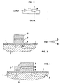
- FIG. 3 schematically illustrates the structure of a so-called stack gate cell.
- This stack gate cell has a source zone 1 and a drain zone 2 in a semiconductor substrate 3.
- the source zone 1 and the drain zone 2 are both n + -doped, while the semiconductor substrate 3 has a p-doping.
- the source zone 1 and the drain zone 2 and the channel region of the semiconductor substrate 3 between the source zone 1 and the drain zone 2 are provided with a tunnel oxide layer 4 made of, for example, silicon dioxide.
- a floating gate 5 made of, for example, polycrystalline silicon is located on the tunnel oxide layer 4 in the region between the drain zone 2 and the source zone 1.
- An intermediate polydielectric 6 and a control gate 7 are also arranged on this floating gate 5.
- FN tunnels For deleting and programming data, such Stack gate cell the so-called "Fowler-Nordheim tunnel" (FN tunnels) can be applied.
- FN tunnels Low-Nordheim tunnels
- 0 V is applied to drain zone 2 and +15 V.
- the control gate 7 applied.
- electrons tunnel out of the Channel area through the tunnel oxide layer 4 into the floating Gate 5.
- programming for example, 0 V is on the control gate 7 and +15 V at drain zone 2, what electrons from the floating gate 5 through the tunnel oxide layer 4 into the Drain zone 2 can tunnel.
- hot-e programming When programming with hot electrons (“hot-e programming") are to the control gate 7, for example +15 V, to the Drain zone 2 + 5V and applied to source zone 1 0V. Thereby electrons migrate from drain zone 2 to the source zone 1 and tunnel simultaneously through the tunnel oxide layer 4 in the floating gate 5.
- an EEPROM is programmable byte and erasable while a flash memory by hot electrons or FN tunnels programmable byte by byte and by FN tunnels can be deleted in blocks.
- FIG. 4 shows, as another type of memory cell, a so-called split-gate cell with a semiconductor substrate 3, an n + -doped source zone 1, an n + -doped drain zone 2, a tunnel oxide layer 4, a floating gate 5, an intermediate polydielectric 6 and a control gate 7.
- the "lowered" part of the control gate 7 is also referred to as the series gate 8, since the increased control gate 7 and the series gate 8 can be regarded as interconnected gates of two NMOS transistors connected in series.
- the stack cell shown in Fig. 3 is by a in this Figure shown on the right, "CG" the control gate 7, "D” the connection of the drain zone 2 and “S” the connection of source zone 1 means.
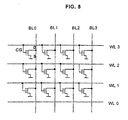
- Memory cells of the type shown in Fig. 3 can be a semiconductor memory with bit lines BL0, BL1, BL2, BL3 and word lines WL0, WL1, WL2 and WL3 form like this schematically is indicated in Fig. 5.
- high voltages are required can be selectively applied to selected word lines or bit lines to delete or to delete individual memory cells program.
- semiconductor memory arrays but also specially regulated voltages with a higher one Constancy than the supply voltage due to high voltages of for example, 15 V can be switched.
- bit lines for flash memories with negative programming voltage
- IEDM International Electron Device Meeting
- a control circuit is used to generate such control voltages needed that the desired voltages with high Should deliver consistency and a small footprint.
- control circuit according to EP 0 154 379 A2 contains a large number of PMOS transistors that are relatively large space requirement and lower electricity yield to have.
- a control circuit is the input mentioned type with the characterizing features of the claim 1 trained.
- the input circuit is composed of one with its source-drain path between a data input and a first data output lying first NMOS transistor and a series connection of two between ground and a second data output lying second and third NMOS transistors are formed, the gate of the second NMOS transistor with gate of the first NMOS transistor and gate of third NMOS transistor with source or drain of the first NMOS transistor are connected. It is expressly noted that such an input circuit is also separate from the Control circuit can be used when using simple Averaging generates a signal and a signal inverted to this should be.
- the control circuit according to the invention can be done with a few Realize components on a small area so that they are on narrowest space in the grid of the memory matrix of the semiconductor memory arrangement can be accommodated.
- the input circuit is made up of just three NMOS transistors, so that they are particularly easy and inexpensive to implement is what semiconductor memory devices or their Grid is of paramount importance. Since there are no PMOS transistors input circuit can be used in a common tub can be accommodated, which is an additional Space advantage means. As a result of the higher current yield of NMOS transistors compared to PMOS transistors can also make the entire circuit particularly small be interpreted.
- the locking circuit can advantageously be made there are two inverters connected in antiparallel.
- Fig. 1 shows the circuit structure of a drive circuit according to the invention.
- This control circuit consists of a Level converter circuit 10, a latch circuit (Latch) 11 and an input circuit 12.
- the level converter circuit 10 consists of PMOS transistors P1, P2 and NMOS transistors N4, N5 and has output connections D and DN on that with the bit lines or word lines of a semiconductor memory device are connected.
- the output lines D or DN represent depending on an input value of "1" or "0", which is connected to an input DATA, a voltage VPROG or 0 V are available.
- the output connection is DN complementary to the output terminal D and delivers 0 V or a voltage VPROG if there is a voltage at the output terminal D. V from VPROG or 0 V.
- VPROG an externally supplied voltage
- the transistors N4, N5, P1 and P2 the Feeding this voltage VPROG to the output connection D or DN controlled, the output DN complementary to the output D is, as has already been explained above.
- a level converter circuit associated with the level converter circuit 10 is similar, is from the aforementioned US-A-5,293,561 known per se.
- the level converter circuit 10 is the latch circuit 11 upstream, which consist of two antiparallel to each other Inverters I1 and I2 exist.
- an input circuit 12 made of three NMOS transistors N1 to N3.
- the data to be saved for example 5 V for a data value "1" are over a Input DATA fed to the input circuit.
- Source or drain of transistor N1 connected to input DATA which also applies to the gate of the transistor N3, the one with the transistor N2 is connected in series.
- Gates of transistors N1 and N2 are connected to one another and to a LOAD connection connected.
- the control circuit according to the invention is particularly well suited for data stored in a non-volatile semiconductor memory device should be programmed. These dates are buffered in the locking circuit 11, and there will be a regulated voltage VPROG for each bit line made available.
- the control circuit is in this Application provided separately for each bit line or word line.
- the data to be programmed is sent to the input line DATA created. With a positive pulse at the connection The data is then LOAD into the latch circuit 11 taken over.
- the signal at the output connection DN is there component to the signal at the output terminal D and delivers 0 V or a voltage VPROG if the voltage at Output terminal D has the value VPROG or 0 V.
- control circuit on a bit line and / or a word line for the general distribution of high voltages.
- the input circuit 12 is only made up of the three NMOS transistors N1, N2 and N3 built. It is special simple and inexpensive to implement, what kind of Memory grid circuits is of paramount importance. There no PMOS transistors can be used, this can Circuit part are generated in a common tub what means a considerable space advantage.
- the input circuit Depending on the input date, 12 pulls the node on the right in FIG. 1 the locking circuit via the transistor N (at the input terminal DATA is "0") at 0 V or the left node to 0 V via transistors N2 and N3.
- the input circuit 12 can be compared to PMOS transistors be designed to be particularly small. Specifically, the sum of the Width of the transistors N2 and N3 may only be as large as the width of a PMOS transistor with a corresponding one CMOS transfer gate (see Fig. 2). For control the input circuit 12 is still only one signal LOAD needed. An additional inverted signal like this is required in itself with a CMOS transfer gate not to be used.
- the control circuit according to the invention does not require an additional one Input inverter for controlling the transistors N4 and N5, but it will do the job of Inverters I1 and I2 of the interlock circuit used.
- the advantageous combination of the locking circuit 11 with the level converter circuit 10 thus saves components and is therefore particularly suitable for use in area-critical Memory grid circuits suitable.
Applications Claiming Priority (3)
| Application Number | Priority Date | Filing Date | Title |
|---|---|---|---|
| DE19725181A DE19725181A1 (de) | 1997-06-13 | 1997-06-13 | Ansteuerschaltung für nichtflüchtige Halbleiter-Speicheranordnung |
| DE19725181 | 1997-06-13 | ||
| PCT/DE1998/001560 WO1998058384A1 (de) | 1997-06-13 | 1998-06-08 | Ansteuerschaltung für nichtflüchtige halbleiter-speicheranordnung |
Publications (2)
| Publication Number | Publication Date |
|---|---|
| EP0988633A1 EP0988633A1 (de) | 2000-03-29 |
| EP0988633B1 true EP0988633B1 (de) | 2001-05-09 |
Family
ID=7832475
Family Applications (1)
| Application Number | Title | Priority Date | Filing Date |
|---|---|---|---|
| EP98936116A Expired - Lifetime EP0988633B1 (de) | 1997-06-13 | 1998-06-08 | Ansteuerschaltung für nichtflüchtige halbleiter-speicheranordnung |
Country Status (12)
| Country | Link |
|---|---|
| US (1) | US6137315A (ja) |
| EP (1) | EP0988633B1 (ja) |
| JP (1) | JP3399547B2 (ja) |
| KR (1) | KR20010013737A (ja) |
| CN (1) | CN1124617C (ja) |
| AT (1) | ATE201112T1 (ja) |
| BR (1) | BR9810100A (ja) |
| DE (2) | DE19725181A1 (ja) |
| ES (1) | ES2157666T3 (ja) |
| RU (1) | RU2221286C2 (ja) |
| UA (1) | UA42887C2 (ja) |
| WO (1) | WO1998058384A1 (ja) |
Families Citing this family (7)
| Publication number | Priority date | Publication date | Assignee | Title |
|---|---|---|---|---|
| DE19921868C2 (de) * | 1999-05-11 | 2001-03-15 | Siemens Ag | Schaltungsanordnung zur Kontrolle von Zuständen einer Speichereinrichtung |
| US7440311B2 (en) * | 2006-09-28 | 2008-10-21 | Novelics, Llc | Single-poly non-volatile memory cell |
| US7554860B1 (en) | 2007-09-21 | 2009-06-30 | Actel Corporation | Nonvolatile memory integrated circuit having assembly buffer and bit-line driver, and method of operation thereof |
| CN101861617B (zh) | 2007-12-28 | 2012-11-28 | 夏普株式会社 | 显示驱动电路和显示装置 |
| WO2009084269A1 (ja) | 2007-12-28 | 2009-07-09 | Sharp Kabushiki Kaisha | 半導体装置及び表示装置 |
| US8718223B2 (en) | 2007-12-28 | 2014-05-06 | Sharp Kabushiki Kaisha | Semiconductor device and display device |
| EP2224423A4 (en) | 2007-12-28 | 2010-12-22 | Sharp Kk | AUXILIARY CAPACITY WIRING CONTROL CIRCUIT AND DISPLAY DEVICE |
Family Cites Families (8)
| Publication number | Priority date | Publication date | Assignee | Title |
|---|---|---|---|---|
| US4599707A (en) * | 1984-03-01 | 1986-07-08 | Signetics Corporation | Byte wide EEPROM with individual write circuits and write prevention means |
| US4716312A (en) * | 1985-05-07 | 1987-12-29 | California Institute Of Technology | CMOS logic circuit |
| US4654547A (en) * | 1985-06-28 | 1987-03-31 | Itt Corporation | Balanced enhancement/depletion mode gallium arsenide buffer/comparator circuit |
| FR2604554B1 (fr) * | 1986-09-30 | 1988-11-10 | Eurotechnique Sa | Dispositif de securite pourla programmation d'une memoire non volatile programmable electriquement |
| JP2773786B2 (ja) * | 1991-02-15 | 1998-07-09 | 日本電気アイシーマイコンシステム株式会社 | 書き込み電圧発生回路 |
| JP3173247B2 (ja) * | 1993-09-29 | 2001-06-04 | ソニー株式会社 | レベルシフタ |
| US5682345A (en) * | 1995-07-28 | 1997-10-28 | Micron Quantum Devices, Inc. | Non-volatile data storage unit method of controlling same |
| JP3404712B2 (ja) * | 1996-05-15 | 2003-05-12 | 株式会社東芝 | 不揮発性半導体記憶装置及びその書き込み方法 |
-
1997
- 1997-06-13 DE DE19725181A patent/DE19725181A1/de not_active Ceased
-
1998
- 1998-06-08 DE DE59800692T patent/DE59800692D1/de not_active Expired - Lifetime
- 1998-06-08 BR BR9810100-5A patent/BR9810100A/pt not_active IP Right Cessation
- 1998-06-08 JP JP50354499A patent/JP3399547B2/ja not_active Expired - Fee Related
- 1998-06-08 KR KR1019997011752A patent/KR20010013737A/ko not_active Application Discontinuation
- 1998-06-08 EP EP98936116A patent/EP0988633B1/de not_active Expired - Lifetime
- 1998-06-08 CN CN98806144A patent/CN1124617C/zh not_active Expired - Fee Related
- 1998-06-08 AT AT98936116T patent/ATE201112T1/de active
- 1998-06-08 UA UA99126788A patent/UA42887C2/uk unknown
- 1998-06-08 WO PCT/DE1998/001560 patent/WO1998058384A1/de not_active Application Discontinuation
- 1998-06-08 RU RU2000100927/09A patent/RU2221286C2/ru not_active IP Right Cessation
- 1998-06-08 ES ES98936116T patent/ES2157666T3/es not_active Expired - Lifetime
-
1999
- 1999-12-13 US US09/460,346 patent/US6137315A/en not_active Expired - Fee Related
Also Published As
| Publication number | Publication date |
|---|---|
| JP3399547B2 (ja) | 2003-04-21 |
| WO1998058384A1 (de) | 1998-12-23 |
| KR20010013737A (ko) | 2001-02-26 |
| DE59800692D1 (de) | 2001-06-13 |
| CN1124617C (zh) | 2003-10-15 |
| CN1260901A (zh) | 2000-07-19 |
| ATE201112T1 (de) | 2001-05-15 |
| UA42887C2 (uk) | 2001-11-15 |
| RU2221286C2 (ru) | 2004-01-10 |
| BR9810100A (pt) | 2000-08-08 |
| EP0988633A1 (de) | 2000-03-29 |
| US6137315A (en) | 2000-10-24 |
| JP2001505350A (ja) | 2001-04-17 |
| ES2157666T3 (es) | 2001-08-16 |
| DE19725181A1 (de) | 1999-02-25 |
Similar Documents
| Publication | Publication Date | Title |
|---|---|---|
| DE4000787C2 (de) | Elektrisch loesch- und programmierbare halbleiterspeichervorrichtung | |
| DE3929816C2 (de) | Elektrisch löschbare und programmierbare Halbleiterspeichereinrichtung und Verfahren zum Löschen und Programmieren dieser Halbleiterspeichereinrichtung | |
| DE4036973C2 (de) | Schaltung zur Erzeugung einer gegenüber einer extern zugeführten Versorgungsspannung erhöhten Lösch- oder Programmierspannung in einer Halbleiter-Speicherschaltung | |
| DE4232025C2 (de) | Elektrisch löschbarer und programmierbarer nichtflüchtiger Halbleiterspeicher mit automatischem Schreibprüfungs-Controller | |
| DE4035660C2 (de) | Elektrisch programmierbare Speichereinrichtung und Verfahren zum Zugreifen/Programmieren von Speicherzellen | |
| DE4233248C2 (de) | Nicht-flüchtige Halbleiterspeichereinrichtung und Verfahren zum blockweisen Löschen von Daten in einer nicht-flüchtigen Halbleiterspeichereinrichtung | |
| DE69434550T2 (de) | Nichtflüchtiges Halbleiterspeicherbauelement, welches die Anforderungen an dessen Spannungsfestigkeit verringert | |
| DE4119394C2 (de) | Nichtflüchtige Halbleiterspeichereinrichtung und Datenlöschungsverfahren hierfür | |
| DE69636178T2 (de) | Verfahren zum Löschen einer Flash EEPROM Speicherzelle | |
| DE4343722C2 (de) | Präzisions-Referenzspannungsschaltung, die sich für die Verwendung in Computersystemen eignet | |
| DE4014117C2 (ja) | ||
| DE3934303C2 (de) | Adreßdecoder für nichtflüchtige Speicher | |
| DE60303511T2 (de) | Verfahren zum löschen eines flash-speichers unter verwendung eines prä-lösch verfahrensschritts | |
| DE3032657A1 (de) | Nichtfluechtige, elektrisch aenderbare statische halbleiter-speicheranordnung mit wahlfreiem zugriff. | |
| DE2742526A1 (de) | Elektrisch programmierbarer mos- festwertspeicher | |
| DE4213741C2 (de) | Speichermatrix mit in Zeilen und Spalten angeordneten Speicherzellen | |
| DE4040492A1 (de) | Automatische loeschoptimierschaltung fuer einen elektrisch loesch- und programmierbaren halbleiterspeicher und automatisches loeschoptimierungsverfahren | |
| DE102004063581A1 (de) | Halbleiterelement | |
| DE3035484A1 (de) | Nicht-fluechtiger halbleiterspeicher | |
| DE2514582C2 (de) | Schaltung zur erzeugung von leseimpulsen | |
| DE2347968A1 (de) | Assoziative speicherschaltung | |
| DE60003451T2 (de) | Wortleitungssignale einer flashspeicher bleiben überall auf dem chip verlustfrei | |
| EP0988633B1 (de) | Ansteuerschaltung für nichtflüchtige halbleiter-speicheranordnung | |
| EP0100772A1 (de) | Elektrisch programmierbare Speichermatrix | |
| DE4135032A1 (de) | Elektrisch loeschbare und programmierbare nur-lese-speichervorrichtung mit einer anordnung von einzel-transistor-speicherzellen |
Legal Events
| Date | Code | Title | Description |
|---|---|---|---|
| PUAI | Public reference made under article 153(3) epc to a published international application that has entered the european phase |
Free format text: ORIGINAL CODE: 0009012 |
|
| 17P | Request for examination filed |
Effective date: 19991206 |
|
| AK | Designated contracting states |
Kind code of ref document: A1 Designated state(s): AT CH DE ES FR GB IT LI |
|
| GRAG | Despatch of communication of intention to grant |
Free format text: ORIGINAL CODE: EPIDOS AGRA |
|
| GRAG | Despatch of communication of intention to grant |
Free format text: ORIGINAL CODE: EPIDOS AGRA |
|
| GRAH | Despatch of communication of intention to grant a patent |
Free format text: ORIGINAL CODE: EPIDOS IGRA |
|
| 17Q | First examination report despatched |
Effective date: 20000929 |
|
| GRAH | Despatch of communication of intention to grant a patent |
Free format text: ORIGINAL CODE: EPIDOS IGRA |
|
| GRAA | (expected) grant |
Free format text: ORIGINAL CODE: 0009210 |
|
| AK | Designated contracting states |
Kind code of ref document: B1 Designated state(s): AT CH DE ES FR GB IT LI |
|
| REF | Corresponds to: |
Ref document number: 201112 Country of ref document: AT Date of ref document: 20010515 Kind code of ref document: T |
|
| REG | Reference to a national code |
Ref country code: CH Ref legal event code: NV Representative=s name: SIEMENS SCHWEIZ AG Ref country code: CH Ref legal event code: EP |
|
| REF | Corresponds to: |
Ref document number: 59800692 Country of ref document: DE Date of ref document: 20010613 |
|
| ITF | It: translation for a ep patent filed |
Owner name: STUDIO JAUMANN P. & C. S.N.C. |
|
| REG | Reference to a national code |
Ref country code: ES Ref legal event code: FG2A Ref document number: 2157666 Country of ref document: ES Kind code of ref document: T3 |
|
| GBT | Gb: translation of ep patent filed (gb section 77(6)(a)/1977) |
Effective date: 20010730 |
|
| ET | Fr: translation filed | ||
| REG | Reference to a national code |
Ref country code: GB Ref legal event code: IF02 |
|
| PLBE | No opposition filed within time limit |
Free format text: ORIGINAL CODE: 0009261 |
|
| STAA | Information on the status of an ep patent application or granted ep patent |
Free format text: STATUS: NO OPPOSITION FILED WITHIN TIME LIMIT |
|
| 26N | No opposition filed | ||
| PGFP | Annual fee paid to national office [announced via postgrant information from national office to epo] |
Ref country code: CH Payment date: 20030520 Year of fee payment: 6 |
|
| PGFP | Annual fee paid to national office [announced via postgrant information from national office to epo] |
Ref country code: ES Payment date: 20030617 Year of fee payment: 6 |
|
| PG25 | Lapsed in a contracting state [announced via postgrant information from national office to epo] |
Ref country code: ES Free format text: LAPSE BECAUSE OF NON-PAYMENT OF DUE FEES Effective date: 20040609 |
|
| PG25 | Lapsed in a contracting state [announced via postgrant information from national office to epo] |
Ref country code: LI Free format text: LAPSE BECAUSE OF NON-PAYMENT OF DUE FEES Effective date: 20040630 Ref country code: CH Free format text: LAPSE BECAUSE OF NON-PAYMENT OF DUE FEES Effective date: 20040630 |
|
| REG | Reference to a national code |
Ref country code: CH Ref legal event code: PL |
|
| PG25 | Lapsed in a contracting state [announced via postgrant information from national office to epo] |
Ref country code: IT Free format text: LAPSE BECAUSE OF NON-PAYMENT OF DUE FEES;WARNING: LAPSES OF ITALIAN PATENTS WITH EFFECTIVE DATE BEFORE 2007 MAY HAVE OCCURRED AT ANY TIME BEFORE 2007. THE CORRECT EFFECTIVE DATE MAY BE DIFFERENT FROM THE ONE RECORDED. Effective date: 20050608 |
|
| REG | Reference to a national code |
Ref country code: ES Ref legal event code: FD2A Effective date: 20040609 |
|
| PGFP | Annual fee paid to national office [announced via postgrant information from national office to epo] |
Ref country code: FR Payment date: 20110630 Year of fee payment: 14 |
|
| PGFP | Annual fee paid to national office [announced via postgrant information from national office to epo] |
Ref country code: GB Payment date: 20110620 Year of fee payment: 14 Ref country code: AT Payment date: 20110613 Year of fee payment: 14 |
|
| PGFP | Annual fee paid to national office [announced via postgrant information from national office to epo] |
Ref country code: DE Payment date: 20110818 Year of fee payment: 14 |
|
| REG | Reference to a national code |
Ref country code: AT Ref legal event code: MM01 Ref document number: 201112 Country of ref document: AT Kind code of ref document: T Effective date: 20120608 |
|
| GBPC | Gb: european patent ceased through non-payment of renewal fee |
Effective date: 20120608 |
|
| REG | Reference to a national code |
Ref country code: FR Ref legal event code: ST Effective date: 20130228 |
|
| PG25 | Lapsed in a contracting state [announced via postgrant information from national office to epo] |
Ref country code: FR Free format text: LAPSE BECAUSE OF NON-PAYMENT OF DUE FEES Effective date: 20120702 Ref country code: DE Free format text: LAPSE BECAUSE OF NON-PAYMENT OF DUE FEES Effective date: 20130101 Ref country code: GB Free format text: LAPSE BECAUSE OF NON-PAYMENT OF DUE FEES Effective date: 20120608 |
|
| REG | Reference to a national code |
Ref country code: DE Ref legal event code: R119 Ref document number: 59800692 Country of ref document: DE Effective date: 20130101 |
|
| PG25 | Lapsed in a contracting state [announced via postgrant information from national office to epo] |
Ref country code: AT Free format text: LAPSE BECAUSE OF NON-PAYMENT OF DUE FEES Effective date: 20120608 |