EP0980065A2 - Einrichtung und Verfahren bei einem Schreibekreis mit Vorverstärker und verminderter Ausstiegs- und Abfallzeit - Google Patents
Einrichtung und Verfahren bei einem Schreibekreis mit Vorverstärker und verminderter Ausstiegs- und Abfallzeit Download PDFInfo
- Publication number
- EP0980065A2 EP0980065A2 EP99113536A EP99113536A EP0980065A2 EP 0980065 A2 EP0980065 A2 EP 0980065A2 EP 99113536 A EP99113536 A EP 99113536A EP 99113536 A EP99113536 A EP 99113536A EP 0980065 A2 EP0980065 A2 EP 0980065A2
- Authority
- EP
- European Patent Office
- Prior art keywords
- current
- circuit
- current source
- write
- source
- Prior art date
- Legal status (The legal status is an assumption and is not a legal conclusion. Google has not performed a legal analysis and makes no representation as to the accuracy of the status listed.)
- Granted
Links
- 238000000034 method Methods 0.000 title claims description 18
- 230000000630 rising effect Effects 0.000 claims 2
- 238000010586 diagram Methods 0.000 description 13
- 230000008859 change Effects 0.000 description 5
- 238000013500 data storage Methods 0.000 description 3
- 230000000694 effects Effects 0.000 description 3
- 230000006870 function Effects 0.000 description 3
- 230000006872 improvement Effects 0.000 description 3
- 238000012986 modification Methods 0.000 description 2
- 230000004048 modification Effects 0.000 description 2
- 230000008569 process Effects 0.000 description 2
- 230000008901 benefit Effects 0.000 description 1
- 238000011022 operating instruction Methods 0.000 description 1
- 230000003287 optical effect Effects 0.000 description 1
- 230000000717 retained effect Effects 0.000 description 1
Images


Classifications
-
- G—PHYSICS
- G11—INFORMATION STORAGE
- G11B—INFORMATION STORAGE BASED ON RELATIVE MOVEMENT BETWEEN RECORD CARRIER AND TRANSDUCER
- G11B19/00—Driving, starting, stopping record carriers not specifically of filamentary or web form, or of supports therefor; Control thereof; Control of operating function ; Driving both disc and head
- G11B19/20—Driving; Starting; Stopping; Control thereof
- G11B19/28—Speed controlling, regulating, or indicating
-
- G—PHYSICS
- G11—INFORMATION STORAGE
- G11B—INFORMATION STORAGE BASED ON RELATIVE MOVEMENT BETWEEN RECORD CARRIER AND TRANSDUCER
- G11B5/00—Recording by magnetisation or demagnetisation of a record carrier; Reproducing by magnetic means; Record carriers therefor
- G11B5/02—Recording, reproducing, or erasing methods; Read, write or erase circuits therefor
- G11B5/09—Digital recording
-
- H—ELECTRICITY
- H03—ELECTRONIC CIRCUITRY
- H03K—PULSE TECHNIQUE
- H03K17/00—Electronic switching or gating, i.e. not by contact-making and –breaking
- H03K17/51—Electronic switching or gating, i.e. not by contact-making and –breaking characterised by the components used
- H03K17/56—Electronic switching or gating, i.e. not by contact-making and –breaking characterised by the components used by the use, as active elements, of semiconductor devices
- H03K17/687—Electronic switching or gating, i.e. not by contact-making and –breaking characterised by the components used by the use, as active elements, of semiconductor devices the devices being field-effect transistors
- H03K17/6871—Electronic switching or gating, i.e. not by contact-making and –breaking characterised by the components used by the use, as active elements, of semiconductor devices the devices being field-effect transistors the output circuit comprising more than one controlled field-effect transistor
- H03K17/6872—Electronic switching or gating, i.e. not by contact-making and –breaking characterised by the components used by the use, as active elements, of semiconductor devices the devices being field-effect transistors the output circuit comprising more than one controlled field-effect transistor using complementary field-effect transistors
Definitions
- the present invention relates to integrated circuits.
- the present invention relates to a system and method for reducing signal rise/fall time for an integrated circuit used in a disk drive assembly.
- a preamplifier is an integrated circuit used in a disk drive assembly to condition and process data which are retrieved from and stored on a magnetic storage medium, such as a magnetic disk.
- "Read” circuits in the preamplifier amplify magnetic signals sensed (retrieved) by a read head flying over the magnetic disk.
- "Write” circuits in the preamplifier apply signals (current pulses) to a write head to be stored as magnetic signals on the disk.
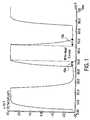
- FIG. 1 An example of current pulses applied to a write head by a write circuit is shown in Figure 1.
- the current creates a magnetic field which is typically stored on a disk.
- the time required for the current to change from its present value to its next value ultimately limits the frequency of the pulses, therefore it is desirable to reduce the rise and fall times 10A - 10B. Accordingly, if the rise/fall speed of the current applied to the write head increases, the writing speed increases.
- the present invention addresses such a need.
- Embodiments of the present invention present preamplifier write circuits for increasing the speed at which a write head in a disk drive assembly writes to a memory, such as a magnetic disk memory.
- the embodiments of the present invention increase the speed at which currents through the write head rise and fall.
- a current source in the write circuit is bypassed during rise and fall times. Bypassing the current source increases the voltage across the write head, increasing in the rise/fall speed of the current pulses applied to the write head.
- the embodiments of the present invention allow data to be written faster than conventional write circuits. Accordingly, the density of the data stored on disk is increased.
- a write circuit for facilitating a write head for writing to a memory, such as a magnetic disk, in a computer system.
- the write circuit comprises a supply voltage source configured to provide current to the write circuit.
- the write circuit also includes a current source coupled to the supply voltage source, the current source being configured to maintain the current at a predetermined value.
- the write circuit also includes a switch coupled to a current source, the switch being configured to bypass the current source during a time when the current is changing.
- a method according to an embodiment of the present invention for facilitating a write head for writing to a memory in a computer system comprising steps of providing a current to a write circuit; changing the current; and bypassing a current source during a time when the current is changing.
- FIG. 2 is a schematic diagram of a conventional preamplifier write circuit.
- the circuit shown in Figure 2 is a common circuit for driving a write head and is commonly referred to as an "H" bridge.
- the magnitude of the write head current is set by reference current sources 20A and 20B.
- Reference current source 20A is reflected through current minor source 22A.
- reference current source 20B is similarly reflected through current mirror source 22B.
- transistors 24A and 26B are driven “on” by voltage sources 34 and 36.
- transistors 24B and 26A are turned “off” by voltage sources 34 and 36.
- a write current (determined by current mirror source 22A) flows from supply voltage 28 through transistor 26B, write head 30, transistor 24A, into current mirror source 22A, and finally into ground 32.
- transistors 24B and 26A are turned “on” while transistors 24A and 26B are turned “off”.
- the current is then routed from supply voltage 28 through transistor 26A, write head 30, transistor 24B, and into current minor source 22B and ground 32.
- the current changes directions through write head 30 when changing from the first half of the write cycle to the second half of the write cycle.
- the intermediate time between the current beginning from a first predetermined value while the current is moving in one direction through write head 30 and the current reaching a second predetermined value while the current is moving in the other direction through write head 30 is the time when the current is changing, such as the rise/fall time.
- V the instantaneous magnitude of the voltage applied across write head 30
- L the write head inductance
- dI/dt the current change per increment of time (i.e., the rise/fall time).
- the larger the applied voltage the greater the rate of current change, hence the smaller the rise/fall time. Smaller rise/fall times facilitate a higher write frequency which allows an increase in the speed of data being written into memory, such as a magnetic disk.
- the largest theoretical available voltage is the supply voltage 28.
- the voltage available to write head 30 is supply voltage 28 reduced by voltage losses across transistors 24B, 24A, 26B, and 26A, and the bias voltage required by current mirror sources 22A and 22B.
- the resistance of the reference current source as represented by current minor sources 22A and 22B, is high relative to the resistance of the remaining transistors 26A, 26B, 24A, and 24B. Accordingly, the resistance of current mirror sources 22A and 22B may be the most significant factor in reducing the voltage available for write head 30.
- the present invention addresses such a need.
- Embodiments of the present invention take advantage of the fact that during the time period when the current is changing, such as rise/fall times, a reference current source for maintaining a predetermined current value is not required. Since the current is changing during rise/fall times, the reference current source is not needed during the rise/fall times to maintain the predetermined value. Only after the changing current has reached its desired final value is it necessary for the reference current source to control and maintain that value.
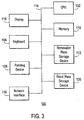
- FIG. 3 is a block diagram of a computer system suitable for implementing embodiments of the present invention.
- Figure 3 illustrates one embodiment of a general purpose computer system.
- Computer system 100 made up of various subsystems described below, includes at least one microprocessor subsystem (also referred to as a central processing unit, or CPU) 102. That is, CPU 102 can be implemented by a single-chip processor or by multiple processors.
- CPU 102 is a general purpose digital processor which controls the operation of the computer system 100. Using instructions retrieved from memory 110, the CPU 102 controls the reception and manipulation of input data, and the output and display of data on output devices.
- CPU 102 is coupled bi-directionally with memory 110 which can include a first primary storage, typically a random access memory (RAM), and a second primary storage area, typically a read-only memory (ROM).
- primary storage can be used as a general storage area and as scratch-pad memory, and can also be used to store input data and processed data. It can also store programming instructions and data, in the form of data objects and text objects, in addition to other data and instructions for processes operating on CPU 102.
- primary storage typically includes basic operating instructions, program code, data and objects used by the CPU 102 to perform its functions.
- Primary storage devices 110 may include any suitable computer-readable storage media, described below, depending on whether, for example, data access needs to be bi-directional or uni-directional.
- CPU 102 can also directly and very rapidly retrieve and store frequently needed data in a cache memory (not shown).
- a removable mass storage device 112 provides additional data storage capacity for the computer system 100, and is coupled either bi-directionally or uni-directionally to CPU 102.
- a specific removable mass storage device commonly known as a CD-ROM typically passes data uni-directionally to the CPU 102, whereas a floppy disk can pass data bi-directionally to the CPU 102.
- Storage 112 may also include computer-readable media such as magnetic tape, flash memory, signals embodied on a carrier wave, PC-CARDS, portable mass storage devices, holographic storage devices, and other storage devices.
- a fixed mass storage 120 can also provide additional data storage capacity. The most common example of mass storage 120 is a hard disk drive.
- Mass storage 112, 120 generally store additional programming instructions, data, and the like that typically are not in active use by the CPU 102. It will be appreciated that the information retained within mass storage 112, 120 may be incorporated, if needed, in standard fashion as part of primary storage 110 (e.g. RAM) as virtual memory.
- primary storage 110 e.g. RAM
- bus 114 can be used to provide access other subsystems and devices as well.
- these can include a display monitor 118, a network interface 116, a keyboard 104, and a pointing device 106, as well as an auxiliary input/output device interface, a sound card, speakers, and other subsystems as needed.
- the pointing device 106 may be a mouse, stylus, track ball, or tablet, and is useful for interacting with a graphical user interface.
- the network interface 116 allows CPU 102 to be coupled to another computer, computer network, or telecommunications network using a network connection as shown. Through the network interface 116, it is contemplated that the CPU 102 might receive information, e.g ., data objects or program instructions, from another network, or might output information to another network in the course of performing the above-described method steps. Information, often represented as a sequence of instructions to be executed on a CPU, may be received from and outputted to another network, for example, in the form of a computer data signal embodied in a carrier wave. An interface card or similar device and appropriate software implemented by CPU 102 can be used to connect the computer system 100 to an external network and transfer data according to standard protocols.
- method embodiments of the present invention may execute solely upon CPU 102, or may be performed across a network such as the Internet, intranet networks, or local area networks, in conjunction with a remote CPU that shares a portion of the processing.
- Additional mass storage devices may also be connected to CPU 102 through network interface 116.
- auxiliary I/O device interface (not shown) can be used in conjunction with computer system 100.
- the auxiliary I/O device interface can include general and customized interfaces that allow the CPU 102 to send and, more typically, receive data from other devices such as microphones, touch-sensitive displays, transducer card readers, tape readers, voice or handwriting recognizers, biometrics readers, cameras, portable mass storage devices, and other computers.
- embodiments of the present invention further relate to computer storage products with a computer readable medium that contain program code for performing various computer-implemented operations.
- the computer-readable medium is any data storage device that can store data which can thereafter be read by a computer system.
- the media and program code may be those specially designed and constructed for the purposes of the present invention, or they may be of the kind well known to those of ordinary skill in the computer software arts.
- Examples of computer-readable media include, but are not limited to, all the media mentioned above: magnetic media such as hard disks, floppy disks, and magnetic tape; optical media such as CD-ROM disks; magneto-optical media such as floptical disks; and specially configured hardware devices such as application-specific integrated circuits (ASICs), programmable logic devices (PLDs), and ROM and RAM devices.
- the computer-readable medium can also be distributed as a data signal embodied in a carrier wave over a network of coupled computer systems so that the computer-readable code is stored and executed in a distributed fashion.
- Examples of program code include both machine code, as produced, for example, by a compiler, or files containing higher level code that may be executed using an interpreter.
- the computer system shown in Figure 3 is but an example of a computer system suitable for use with the invention.
- Other computer systems suitable for use with the invention may include additional or fewer subsystems.
- bus 114 is illustrative of any interconnection scheme serving to link the subsystems.
- Other computer architectures having different configurations of subsystems may also be utilized.
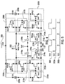
- FIG 4 is a schematic diagram of a write circuit according to a first embodiment of the present invention.
- transistors 214A and 214B serve as switches which seize control of the current such that current mirror sources 212A and 212B are unable to draw the current during rise/fall times. Accordingly, current minor sources 212A and 212B are bypassed during rise/fall times.
- the magnitude of the write head current is set by reference current sources 206A and 206B during times when the current is not changing (non-rise/fall times).
- Reference current source 206A is reflected by current minor source 212A and 230A, while reference current source 206B is similarly reflected through current minor source 212B and 230B.
- transistors 210B and 208A are driven "on" by voltage sources 218A and 218B.
- a write current (determined by current minor source 212B and 230B) flows from supply voltage 200 through transistor 208A, and through write head 202 and through transistor 210B.
- transistor 214B is turned “on” by a voltage source 216B.
- Transistor 214B is switched on, thus providing a low resistance path to ground 204 in shunt with current mirror source 212B.
- Being "in shunt" with current minor source 212B is understood to mean that transistor 214B acts as a switch across current minor source 212B such that current minor source 212B no longer operates to maintain the current at a predetermined value.
- transistor 214B obtains control of the current and forces the current to flow through transistor 214B rather than through current minor source 212B.
- transistor 214B When the current is no longer substantially changing (no longer in rise/fall time), then transistor 214B is turned “off' and the current is allowed to flow through current minor source 212B. The time that transistor 214B is switched "on” is user configurable.
- current minor source 212B is bypassed.
- reference current source 206B is reflected in current minor source 212B and transistor 214B is turned "off".
- transistors 208A and 210B are turned “off", while transistors 208B and 210A are turned “on”. Accordingly, current flows from supply voltage 200 through transistor 208B and through write head 202, and through transistor 210A. During rise/fall times, the current flows from write head 202 through transistor 210A and into transistor 214A. During rise/fall times of the second half cycle, transistor 214A is switched “on” by voltage source 216A, thus providing a low resistance path to ground in shunt with current minor source 212A.
- the voltage that is provided across write head 202 during rise/fall times is approximately source voltage 200 reduced by voltage losses across transistors 208A-208B, 210A-210B, and transistors 214A-214B. Since transistors 214A and 214B provide a low resistance path to ground 204 in shunt with current mirror sources 212A - 212B, no head voltage is lost due to current mirror sources 212A-212B during rise/fall times. Additionally, since the voltage loss across transistors 214A-214B are substantially less than the voltage loss across current minor sources 212A-212B, there is more voltage available to be applied to write head 202 during rise/fall times. Thus, a minimum amount of voltage is subtracted from supply voltage 200 and a maximum amount of voltage is applied across write head 202. Accordingly, the circuit of Figure 4 maximizes the voltage across write head 202 when the current is changing.
- Figure 5 is an illustration of signals applied to the write circuit shown in Figure 4 according to an embodiment of the present invention.
- Signal 300 is a signal typical of one produced by voltage source 218A, and the opposite phase signal would be produced by voltage source 218B.
- Signal 302A is a signal produced by voltage source 216A to be applied to transistor 214A.
- Signal 302B is a signal produced by voltage source 216B to be applied to transistor 214B.
- Figure 5 shows that voltage signal 302A is turned on at the rise time of the voltage signal 300.
- voltage signal 302B is turned on at the fall time of signal 300. Accordingly, during rise and fall times, voltage sources 216A and 216B are turned "on" alternately through out the rise/fall times of the write cycle to alternately turn on transistors 214A-214B.
- the time during which transistors 214A and 214B are turned “on” is user configurable. It is estimated that the risetime ranges from 0.5 nano seconds to 4 nano seconds, depending on various equipment used in conjunction with the write circuit. Since disk drive manufacturers choose the type of write heads used in the drive assembly, the time during which transistors 214A and 214B are turned “on” is configurable based on the type of write head and the manufacturer's predetermined current values selected during the initial alignment of the drive assembly.
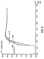
- Figure 6 is a graph comparing rise time between a circuit according to an embodiment of the present invention and a conventional circuit, such as the circuit shown in Figure 2. Results for rise times are similar to results for fall times. Result 400 represents the rise time of a current according to an embodiment of the present invention, such as the circuit shown in Figure 4, while result 402 represents rise time according to a conventional circuit, such as that shown in Figure 2. It is estimated that the improvement shown in this diagram, facilitated by an embodiment of the present invention, may be approximately 315 pico seconds. An estimated average of improved risetime may be approximately 150 pico seconds. However, an improvement in the risetime may be as much as 400 pico seconds. Improvements depend heavily on customer hardware selection and preferences on load and various equipment.
- FIG. 7 is a schematic diagram of a write circuit according to a second embodiment of the present invention.
- the difference between the circuit shown in Figure 7 and the circuit shown in Figure 4 is that transistors 214A' and 214B' are directly connected to write head 202' through connections 240A and 240B. Accordingly, during rise/fall times, the current flows from write head 202' directly to transistors 214A' and 214B' during alternate half cycles of the write cycle. During the remainder of the write cycle (non-rise/fall times), the current flows through current mirror sources 212A' and 212B'. Accordingly, in this embodiment, transistors 210A' and 210B' are bypassed during rise/fall times as well as current mirror sources 212A' and 212B'.
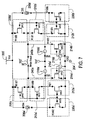
- FIG 8 is a schematic diagram of a write circuit according to a third embodiment of the present invention.
- current mirror sources 212A'' and 212B'' are turned “on" and bypass current to ground themselves during rise/fall times.
- Reference current sources 206A'' and 206B'' are still coupled to current minor sources 212A'', 230A'' and 212B'', 230B''.
- there is another transistor 400A located between reference current source 206A'' and current mirror source 230A'', 212A''.
- a transistor 400B is located between reference current source 206B'' and current minor source 230B'', 212B''.
- transistor 402A is in shunt with reference current source 206A''.
- Transistor 402A is also shown to be coupled to transistor 400A and a voltage source 216A''.
- Transistor 402A is also coupled with transistor 212A'' through connection 450A.
- transistor 402B is in shunt with reference current source 206B''.
- Transistor 402B is also shown to be coupled to transistor 400B and a voltage source 216B''.
- Transistor 402B is also coupled with transistor 212B'' through connection 450B.
- transistor 400B is turned “off” while transistor 402B is turned “on”.
- a signal generated by voltage source 216B'' turns transistor 402B'' "on” and transistor 400B'' "off", which turns transistor 212B'' "on”.
- the signal generated by voltage source 216B'' is the antiphase counterparts of signal 302B of Figure 5.
- transistor 212B'' serves the same function as transistor 214B of Figure 4 and 214B' of Figure 7 during rise/fall time.
- current mirrors 212B and 212B' were bypassed by transistors 214B and 214B'.
- current mirror 212B'' is in effect made to bypass itself by using the combination of transistors 402B , 400B and voltage source 216B'' shown in Figure 8. During rise/fall times, transistor 212B'' no longer acts as a current mirror source, but rather as a low resistance transistor bypassing current to ground.
- the current flows from the source voltage 200'' through transistor 208A'', through write head 202'', and through transistor 212B''.
- Transistor 212B'' is switched "on" by voltage source 216B'' such that the resistance of transistor 212B'' is substantially less than the resistance which would have been generated by a current mirror source.
- transistor 402B is turned “off” and transistor 400B is turned “on", such that transistors 212B'' and 230B'' act together to work as current mirror sources.
- transistor 400A is turned “off” while transistor 402A is turned “on”.
- a signal generated by voltage source 216A'' turns transistor 402A "on” and transistor 400A “off", which turns transistor 212A'' "on”.
- the signal generated by voltage source 216A'' is the antiphase counterpart of signal 302A of Figure 5. Accordingly, transistor 212A'' serves the same function as transistor 214A of Figure 4 and 214A' of Figure 7 during rise/fall time.
- the current flows from the source voltage 200'' through transistor 208B'', through write head 202'', and through transistor 212A''.
- Transistor 212A'' is switched on by voltage source 216A'' such that the resistance of transistor 212A'' is substantially less than the resistance which would have been associated with a current mirror source.
- transistor 402A is turned “off” and transistor 400A is turned “on", such that transistors 212A'' and 230A'' act together to work as current mirror sources.
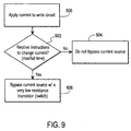
- Figure 9 is a flow diagram of a method according to embodiments of the present invention for providing a shorter time for writing data into memory by reducing rise/fall times.
- a current is applied to a write circuit (step 500). It is then determined whether instructions have been received to change the current (i.e. rise/fall time) (step 502). The instruction for changing the current is typically expected to be received from a controller in a disk drive assembly. If the current is not changing, then the reference current source is not bypassed (step 504). If, however, the current is changing (i.e. rise/fall time), then the reference current source is bypassed with a very low resistance transistor (switch) (step 506).
- switch very low resistance transistor
- bypassing is herein meant to include a situation wherein the mirror current source in effect bypasses itself, as well as a situation wherein the mirror current source is bypassed due to another device, such as a transistior, working in shunt with the mirror current source.
Landscapes
- Digital Magnetic Recording (AREA)
Applications Claiming Priority (2)
| Application Number | Priority Date | Filing Date | Title |
|---|---|---|---|
| US09/131,766 US6222695B1 (en) | 1998-08-10 | 1998-08-10 | System and method for a preamplifier write circuit with reduced rise/fall time |
| US131766 | 1998-08-10 |
Publications (3)
| Publication Number | Publication Date |
|---|---|
| EP0980065A2 true EP0980065A2 (de) | 2000-02-16 |
| EP0980065A3 EP0980065A3 (de) | 2000-03-15 |
| EP0980065B1 EP0980065B1 (de) | 2006-02-08 |
Family
ID=22450932
Family Applications (1)
| Application Number | Title | Priority Date | Filing Date |
|---|---|---|---|
| EP99113536A Expired - Lifetime EP0980065B1 (de) | 1998-08-10 | 1999-07-06 | Einrichtung und Verfahren bei einem Schreibekreis mit Vorverstärker und verminderter Ausstiegs- und Abfallzeit |
Country Status (7)
| Country | Link |
|---|---|
| US (1) | US6222695B1 (de) |
| EP (1) | EP0980065B1 (de) |
| JP (1) | JP2000057509A (de) |
| KR (1) | KR20000017217A (de) |
| DE (1) | DE69929730T2 (de) |
| SG (1) | SG74153A1 (de) |
| TW (1) | TW425595B (de) |
Cited By (1)
| Publication number | Priority date | Publication date | Assignee | Title |
|---|---|---|---|---|
| US8421510B2 (en) | 2010-06-15 | 2013-04-16 | Texas Instruments Incorporated | Low voltage high-speed wave shaping circuitry |
Families Citing this family (7)
| Publication number | Priority date | Publication date | Assignee | Title |
|---|---|---|---|---|
| JP2002230710A (ja) | 2001-02-05 | 2002-08-16 | Mitsubishi Electric Corp | 磁気記録書き込み回路 |
| US7292400B2 (en) * | 2001-04-23 | 2007-11-06 | Seagate Technology Llc | Device for limiting current in a sensor |
| US6879456B2 (en) * | 2002-08-15 | 2005-04-12 | Agere Systems Inc. | Disk drive writer with active reflection cancellation |
| US7417817B1 (en) | 2003-03-18 | 2008-08-26 | Marvell International Ltd. | Write driver circuit for magnetic data storage systems |
| US7746590B2 (en) * | 2004-10-06 | 2010-06-29 | Agere Systems Inc. | Current mirrors having fast turn-on time |
| US7583459B1 (en) | 2004-11-18 | 2009-09-01 | Marvell International Ltd. | Method and apparatus for write precompensation in a magnetic recording system |
| US7408313B1 (en) * | 2005-08-23 | 2008-08-05 | Marvell International Ltd. | Low power preamplifier writer architecture |
Family Cites Families (18)
| Publication number | Priority date | Publication date | Assignee | Title |
|---|---|---|---|---|
| US3618119A (en) | 1970-03-13 | 1971-11-02 | Storage Technology Corp | Compensation in a magentic write circuit |
| US4551772A (en) | 1984-03-28 | 1985-11-05 | Storage Technology Corporation | Write drive with current mirrors which reduce feed-through |
| JPH081754B2 (ja) | 1986-06-10 | 1996-01-10 | 日本電気株式会社 | メモリ回路 |
| JP2701652B2 (ja) | 1992-04-08 | 1998-01-21 | 日本電気株式会社 | 磁気ヘッド駆動回路 |
| US5287231A (en) | 1992-10-06 | 1994-02-15 | Vtc Inc. | Write circuit having current mirrors between predriver and write driver circuits for maximum head voltage swing |
| US5296975A (en) | 1992-10-09 | 1994-03-22 | International Business Machines Corporation | High-transition-rate, low-supply-voltage write driver circuitry for magnetic inductive write head |
| US5291069A (en) | 1992-12-15 | 1994-03-01 | International Business Machines Corporation | Bipolar H write driver |
| US5386328A (en) | 1993-06-18 | 1995-01-31 | Silicon Systems, Inc. | Current mirror based write driver |
| JP2586802B2 (ja) | 1993-10-12 | 1997-03-05 | 日本電気株式会社 | 磁気記録・再生装置 |
| EP0764321B1 (de) | 1994-06-10 | 2001-11-28 | Koninklijke Philips Electronics N.V. | Anordnung zur aufzeichnung eines informationssignals auf einen magnetaufzeichnungsträger |
| JP3537891B2 (ja) | 1994-10-24 | 2004-06-14 | 株式会社ルネサステクノロジ | ライトドライバ回路と半導体集積回路装置 |
| US5751171A (en) | 1995-03-22 | 1998-05-12 | Vtc Inc. | Predriver for fast current switching through a two-terminal inductive load |
| US5612828A (en) | 1995-09-11 | 1997-03-18 | Vtc Inc. | Write driver with improvements for risetime |
| KR100449934B1 (ko) * | 1995-11-21 | 2004-12-14 | 코닌클리케 필립스 일렉트로닉스 엔.브이. | 자기기록헤드와,용량성피드-포워드보상기능을지닌기록증폭기를포함하는장치 |
| JP2654380B2 (ja) | 1995-11-27 | 1997-09-17 | ローム株式会社 | 磁気ディスク記録回路 |
| US5822141A (en) * | 1996-03-27 | 1998-10-13 | International Business Machines Corporation | High speed FET write driver for an inductive head |
| US5661680A (en) | 1996-09-09 | 1997-08-26 | International Business Machines Corporation | Analog output buffer circuit |
| US5869988A (en) * | 1997-03-25 | 1999-02-09 | Marvell Technology Group, Ltd. | High speed write driver for inductive heads |
-
1998
- 1998-08-10 US US09/131,766 patent/US6222695B1/en not_active Expired - Lifetime
-
1999
- 1999-06-23 TW TW088110548A patent/TW425595B/zh not_active IP Right Cessation
- 1999-07-06 DE DE69929730T patent/DE69929730T2/de not_active Expired - Lifetime
- 1999-07-06 EP EP99113536A patent/EP0980065B1/de not_active Expired - Lifetime
- 1999-07-21 SG SG1999003494A patent/SG74153A1/en unknown
- 1999-08-09 JP JP11225548A patent/JP2000057509A/ja active Pending
- 1999-08-10 KR KR1019990032719A patent/KR20000017217A/ko not_active Withdrawn
Cited By (1)
| Publication number | Priority date | Publication date | Assignee | Title |
|---|---|---|---|---|
| US8421510B2 (en) | 2010-06-15 | 2013-04-16 | Texas Instruments Incorporated | Low voltage high-speed wave shaping circuitry |
Also Published As
| Publication number | Publication date |
|---|---|
| EP0980065B1 (de) | 2006-02-08 |
| DE69929730D1 (de) | 2006-04-20 |
| EP0980065A3 (de) | 2000-03-15 |
| US6222695B1 (en) | 2001-04-24 |
| SG74153A1 (en) | 2000-07-18 |
| TW425595B (en) | 2001-03-11 |
| DE69929730T2 (de) | 2006-09-21 |
| JP2000057509A (ja) | 2000-02-25 |
| KR20000017217A (ko) | 2000-03-25 |
Similar Documents
| Publication | Publication Date | Title |
|---|---|---|
| JPH07105682A (ja) | ダイナミックメモリ装置 | |
| JPH0330185A (ja) | メモリ素子の出力バッファのプレチャージ制御回路 | |
| EP0980065B1 (de) | Einrichtung und Verfahren bei einem Schreibekreis mit Vorverstärker und verminderter Ausstiegs- und Abfallzeit | |
| EP0759621A2 (de) | Leseverstärker für statischen Direktzugriffspeicher | |
| US5585701A (en) | Current mirror circuit constituted by FET (field effect transistor) and control system using the same | |
| JPH08321196A (ja) | 集積回路形式メモリの読出のための電流検出回路 | |
| JPH11273350A (ja) | 半導体装置及びプリチャージ方法 | |
| US6271978B1 (en) | Power efficient overshoot control for magnetic recording write driver | |
| US20050254159A1 (en) | Disk drive write driver with boosting circuit to improve output voltage swing | |
| JPS6257318A (ja) | Ttlレベル入力を受信するcmosバツフア回路 | |
| JPH10269772A (ja) | 半導体記憶装置 | |
| JP2002123902A (ja) | メモリディスクへ書込むための書込ヘッドドライバ回路及び方法 | |
| EP1587066B1 (de) | Schreibtreiber mit Spannungs-Erhöhung und Verbindung mit angepasster Impedanz | |
| JP2001256790A (ja) | 低電源電圧検知回路 | |
| US20050174673A1 (en) | Apparatus and method for applying write signals for driving a write head | |
| JP3204200B2 (ja) | 半導体メモリ装置 | |
| JP2923985B2 (ja) | Eeprom装置 | |
| JP2003302301A (ja) | 半導体物理量センサ装置 | |
| KR100557996B1 (ko) | 반도체 메모리 장치 | |
| JPH0831180A (ja) | 半導体記憶装置 | |
| JPS6150279A (ja) | 半導体メモリ | |
| US20020105312A1 (en) | Charge pump based negative regulator with adjustable output current to allow reduction of switching noise | |
| US6205058B1 (en) | Data input/output circuit for performing high speed memory data read operation | |
| JPS619893A (ja) | Mos型メモリ装置 | |
| JP3024036B2 (ja) | 半導体記憶装置の出力バッファ回路 |
Legal Events
| Date | Code | Title | Description |
|---|---|---|---|
| PUAI | Public reference made under article 153(3) epc to a published international application that has entered the european phase |
Free format text: ORIGINAL CODE: 0009012 |
|
| PUAL | Search report despatched |
Free format text: ORIGINAL CODE: 0009013 |
|
| AK | Designated contracting states |
Kind code of ref document: A2 Designated state(s): DE FR GB IT |
|
| AX | Request for extension of the european patent |
Free format text: AL;LT;LV;MK;RO;SI |
|
| AK | Designated contracting states |
Kind code of ref document: A3 Designated state(s): AT BE CH CY DE DK ES FI FR GB GR IE IT LI LU MC NL PT SE |
|
| AX | Request for extension of the european patent |
Free format text: AL;LT;LV;MK;RO;SI |
|
| 17P | Request for examination filed |
Effective date: 20000511 |
|
| AKX | Designation fees paid |
Free format text: DE FR GB IT |
|
| GRAP | Despatch of communication of intention to grant a patent |
Free format text: ORIGINAL CODE: EPIDOSNIGR1 |
|
| GRAS | Grant fee paid |
Free format text: ORIGINAL CODE: EPIDOSNIGR3 |
|
| GRAA | (expected) grant |
Free format text: ORIGINAL CODE: 0009210 |
|
| RAP1 | Party data changed (applicant data changed or rights of an application transferred) |
Owner name: INFINEON TECHNOLOGIES NORTH AMERICA CORP. |
|
| AK | Designated contracting states |
Kind code of ref document: B1 Designated state(s): DE FR GB IT |
|
| REG | Reference to a national code |
Ref country code: GB Ref legal event code: FG4D |
|
| REF | Corresponds to: |
Ref document number: 69929730 Country of ref document: DE Date of ref document: 20060420 Kind code of ref document: P |
|
| PG25 | Lapsed in a contracting state [announced via postgrant information from national office to epo] |
Ref country code: GB Free format text: LAPSE BECAUSE OF NON-PAYMENT OF DUE FEES Effective date: 20060706 |
|
| ET | Fr: translation filed | ||
| PLBE | No opposition filed within time limit |
Free format text: ORIGINAL CODE: 0009261 |
|
| STAA | Information on the status of an ep patent application or granted ep patent |
Free format text: STATUS: NO OPPOSITION FILED WITHIN TIME LIMIT |
|
| 26N | No opposition filed |
Effective date: 20061109 |
|
| GBPC | Gb: european patent ceased through non-payment of renewal fee |
Effective date: 20060706 |
|
| REG | Reference to a national code |
Ref country code: FR Ref legal event code: TP |
|
| REG | Reference to a national code |
Ref country code: FR Ref legal event code: TP |
|
| PGFP | Annual fee paid to national office [announced via postgrant information from national office to epo] |
Ref country code: IT Payment date: 20140724 Year of fee payment: 16 |
|
| PG25 | Lapsed in a contracting state [announced via postgrant information from national office to epo] |
Ref country code: IT Free format text: LAPSE BECAUSE OF NON-PAYMENT OF DUE FEES Effective date: 20150706 |
|
| REG | Reference to a national code |
Ref country code: FR Ref legal event code: PLFP Year of fee payment: 18 |
|
| REG | Reference to a national code |
Ref country code: FR Ref legal event code: PLFP Year of fee payment: 19 |
|
| REG | Reference to a national code |
Ref country code: FR Ref legal event code: PLFP Year of fee payment: 20 |
|
| PGFP | Annual fee paid to national office [announced via postgrant information from national office to epo] |
Ref country code: FR Payment date: 20180726 Year of fee payment: 20 Ref country code: DE Payment date: 20180727 Year of fee payment: 20 |
|
| REG | Reference to a national code |
Ref country code: DE Ref legal event code: R071 Ref document number: 69929730 Country of ref document: DE |