EP0764321B1 - Anordnung zur aufzeichnung eines informationssignals auf einen magnetaufzeichnungsträger - Google Patents
Anordnung zur aufzeichnung eines informationssignals auf einen magnetaufzeichnungsträger Download PDFInfo
- Publication number
- EP0764321B1 EP0764321B1 EP95918712A EP95918712A EP0764321B1 EP 0764321 B1 EP0764321 B1 EP 0764321B1 EP 95918712 A EP95918712 A EP 95918712A EP 95918712 A EP95918712 A EP 95918712A EP 0764321 B1 EP0764321 B1 EP 0764321B1
- Authority
- EP
- European Patent Office
- Prior art keywords
- terminal
- current
- transistor
- main electrode
- write
- Prior art date
- Legal status (The legal status is an assumption and is not a legal conclusion. Google has not performed a legal analysis and makes no representation as to the accuracy of the status listed.)
- Expired - Lifetime
Links
Images

Classifications
-
- G—PHYSICS
- G11—INFORMATION STORAGE
- G11B—INFORMATION STORAGE BASED ON RELATIVE MOVEMENT BETWEEN RECORD CARRIER AND TRANSDUCER
- G11B5/00—Recording by magnetisation or demagnetisation of a record carrier; Reproducing by magnetic means; Record carriers therefor
- G11B5/02—Recording, reproducing, or erasing methods; Read, write or erase circuits therefor
- G11B5/022—H-Bridge head driver circuit, the "H" configuration allowing to inverse the current direction in the head
-
- G—PHYSICS
- G11—INFORMATION STORAGE
- G11B—INFORMATION STORAGE BASED ON RELATIVE MOVEMENT BETWEEN RECORD CARRIER AND TRANSDUCER
- G11B5/00—Recording by magnetisation or demagnetisation of a record carrier; Reproducing by magnetic means; Record carriers therefor
- G11B5/02—Recording, reproducing, or erasing methods; Read, write or erase circuits therefor
-
- H—ELECTRICITY
- H03—ELECTRONIC CIRCUITRY
- H03K—PULSE TECHNIQUE
- H03K17/00—Electronic switching or gating, i.e. not by contact-making and –breaking
- H03K17/51—Electronic switching or gating, i.e. not by contact-making and –breaking characterised by the components used
- H03K17/56—Electronic switching or gating, i.e. not by contact-making and –breaking characterised by the components used by the use, as active elements, of semiconductor devices
- H03K17/60—Electronic switching or gating, i.e. not by contact-making and –breaking characterised by the components used by the use, as active elements, of semiconductor devices the devices being bipolar transistors
- H03K17/66—Switching arrangements for passing the current in either direction at will; Switching arrangements for reversing the current at will
- H03K17/661—Switching arrangements for passing the current in either direction at will; Switching arrangements for reversing the current at will connected to both load terminals
- H03K17/662—Switching arrangements for passing the current in either direction at will; Switching arrangements for reversing the current at will connected to both load terminals each output circuit comprising more than one controlled bipolar transistor
- H03K17/663—Switching arrangements for passing the current in either direction at will; Switching arrangements for reversing the current at will connected to both load terminals each output circuit comprising more than one controlled bipolar transistor using complementary bipolar transistors
Definitions
- the invention relates to an arrangement for recording an information signal on a magnetic record carrier, comprising a write head for recording information on the record carrier, and a write amplifier for driving the write head in response to the information signal, the write amplifier comprising: a first write terminal and a second write terminal, which are coupled to the write head;
- the invention also relates to a write amplifier for use in such an arrangement.
- bit change is influenced by the common-mode voltage just before the change, which may give rise to bit-pattern-dependent signal distortion.
- the fluctuating common-mode voltage may produce crosstalk to other sensitive circuits.
- the write head is now connected between the high-impedance outputs of four current mirrors, which are turned on two at a time by means of the switchable current sources.
- the first switchable current source conducts a current will flow through the write head from the first supply terminal to the second supply terminal via the first and the fourth current mirror.
- the second switchable current source conducts an opposite current will flow through the write head from the first supply terminal to the second supply terminal via the second and the third current mirror. Since the write head is connected between the high-impedance current output terminals of the four current mirrors the common-mode voltage can be fixed as required by additional measures, preferably at half the supply voltage, and can be rendered independent of the bit pattern.
- the current mirrors then saturate only during the peaks of the write head voltage and no clamping circuits are needed to preclude oversaturation of the output transistors of the write amplifier.
- a first embodiment of an arrangement in accordance with the invention with common-mode control is characterised in that the write amplifier further comprises: a first resistor connected between the first write terminal and a first node, a second resistor connected between the first node and the second write terminal, a third resistor connected between the first supply terminal and the first node, and a fourth resistor connected between the second supply terminal and the first node.
- the first and the second resistor are arranged in series across the write head and also form damping resistors for the write head.
- the common-mode voltage across the write head is equal to the voltage on the first node, which forms the centre tap of the first and the second resistor, and is fixed by means of a simple voltage divider arranged across the power supply and comprising the third and the fourth resistor. The fixation of the common-mode voltage improves as the impedance of the voltage divider is reduced. Too low an impedance is to be avoided in view of the increasing dissipation in the voltage divider.
- a second embodiment of the arrangement in accordance with the invention is characterised in that the write amplifier further comprises: a first resistor connected between the first write terminal and a first node, a second resistor connected between the first node and the second write terminal, a first transistor of a first conductivity type having a control electrode, a first main electrode connected to the first node and a second main electrode coupled to the first supply terminal, a second transistor of the first conductivity type having a control electrode connected to the control electrode of the first transistor, a first main electrode, and a second main electrode connected to the control electrode of the second transistor, a third resistor connected between the first supply terminal and the second main electrode of the second transistor, a third transistor of a second conductivity type having a control electrode, a first main electrode connected to the first node and a second main electrode coupled to the second supply terminal, a fourth transistor of the second conductivity type having a control electrode connected to the control electrode of the third transistor, a first main electrode connected to the first main electrode
- the first and the second transistor operate in class A/B and produce at the first node a low impedance, which can be realised with comparatively larger third and fourth resistors.
- the transistors may be bipolar transistors or unipolar MOS transistors.
- the control electrode, the first main electrode and the second main electrode correspond to the base, the emitter and the collector, respectively, for a bipolar transistor and to the gate, the source and the drain, respectively, for a unipolar transistor.
- a third embodiment of an arrangement with common mode control in accordance with the invention is characterised in that the write amplifier further comprises:
- This embodiment advantageously combines the common-mode control and the quiescent current setting for the four current mirrors.
- the bias currents through the four transistors connected to the first and the second node are not drained to the supply terminals but flow into the respective current input terminals of the four current mirrors and serve as quiescent currents for the current mirrors.
- the damping resistance is made up of two series chains of two resistors having a centre tap at the first and the second node.
- the current mirrors reduce the apparent resistance of the damping resistors for common-mode signals by a factor determined by the current gain of the current mirrors.
- the individual series chains function as emitter degeneration resistors for the first and the fourth transistor, whose emitters are connected to the first node, and for the third and the sixth transistor, whose emitters are connected to the second node. This reduces the influence of a possible mismatch between the first and the third transistor and between the fourth and the sixth transistor.
- An alternative embodiment is characterised in that the second node is connected to the first node.
- first and second switchable current sources determine how much and in which direction current flows through the write head.
- first and the second switchable current source comprise:
- the bias current source determines the magnitude of the write current through the write head.
- the bias current is drained to the power supply via the eighth transistor or via the twelfth transistor, depending on the value of the information signal.
- the seventh, the ninth and the tenth transistor form a translinear loop with the eighth transistor, and the eleventh, the thirteenth and the tenth transistor form a translinear loop with the twelfth transistor.
- Conduction of the eighth or the twelfth transistor now results in an amplified current flowing from the first current input terminal to the third current input terminal via the seventh and the ninth transistor or from the second current input terminal to the fourth current input terminal.
- the switchable current sources thus form floating switchable current sources whose switching signals have d.c. levels which can be chosen freely.
- the buffers for the information signal can be emitter followers or source followers.
- the quiescent current supply for these followers can be combined advantageously with the current supply for the switchable current sources.
- an embodiment of the arrangement is further characterised in that the first and the second switchable current source further comprise: a fourteenth transistor of the first conductivity type having a control electrode for receiving the information signal, a first main electrode connected to the third node and a second main electrode coupled to the first supply terminal, a fifteenth transistor of the first conductivity type having a control electrode for receiving the information signal, a first main electrode connected to the fifth node and a second main electrode coupled to the first supply terminal, a sixteenth transistor of the first conductivity type having a control electrode connected to the control electrode of the eighth transistor, a first main electrode connected to the first main electrode of the eighth transistor, and a second main electrode coupled to the fifth node, a seventeenth transistor of the first conductivity type having a control electrode connected to the control electrode of the twelfth transistor, a first main electrode connected to the first main
- the fourteenth and the fifteenth transistor operate as signal followers and buffer the information signal.
- the currents through these transistors now flow to the fourth node through the eighth and the twelfth transistor, respectively.
- the sixteenth and the seventeenth transistor ensure that always one half of the bias current from the bias current source flows through one signal follower and the other half through the other signal follower.
- Parasitic capacitances at the first and the second write terminal caused by the transistors of the write amplifier and by the wiring and construction of the write head limit the bit rate of the information signal to be recorded. This is because for high frequencies the write current is shunted by the parasitic capacitances.
- the write amplifier further comprises at least one of:
- the first to the fourth capacitor neutralise the parasitic capacitances by injecting opposite capacitive currents into the first and the second write terminal.
- the capacitors are used in pairs, i.e. the first together with the second and/or the third together with the fourth capacitor, in order not to disturb the symmetry of the arrangement and not to load the common mode.
- the four current mirrors may be of any suitable type.
- the third current mirror and the fourth current mirror each comprise a diode-connected input transistor of a first conductivity type having a control electrode and a second main electrode connected to the third and the fourth current input terminal, respectively, and having a first main electrode coupled to the second supply terminal, and an output transistor of the first conductivity type having a control electrode connected to the control electrode of the relevant input transistor, a first main electrode coupled to the second supply terminal, and a second main electrode connected to the third and the fourth current output terminal, and in that
- This embodiment may be characterised further in that the first main electrodes of the input transistors and output transistors of the first and the second current mirror are connected to the first supply terminal via resistors, and the first main electrodes of the input transistors and output transistors of the third and the fourth current mirror are connected to the second supply terminal via resistors.
- the resistors provide a better matching between the current mirror transistors and improve the temperature stability.
- Figure 1 shows the basic structure of an arrangement for recording an information signal on a magnetic record carrier in accordance with the invention.
- the arrangement comprises a write head 2 for recording information on the record carrier (not shown) and a write amplifier 4 for driving the write head 2 in response to the information signal.
- the write amplifier has a first write terminal 6 and a second write terminal 8, which are coupled to the write head 2 to supply a write current.
- a first supply terminal 10 and a second supply terminal 12 serve for connection of a supply voltage for the write amplifier. In the present case the second supply terminal 12 is connected to signal earth.
- the amplifier 4 comprises a first current mirror 14 having a first current input terminal 16, a first current output terminal 18 coupled to the first write terminal 6, and a first common current terminal 20 connected to the first supply terminal 10; a second current mirror 22 having a second current input terminal 24, a second current output terminal 26 coupled to the second write terminal 8, and a second common current terminal 28 connected to the first supply terminal 10; a third current mirror 30 having a third current input terminal 32, a third current output terminal 34 coupled to the first write terminal 6, and a third common current terminal 36 connected to the second supply terminal 12; a fourth current mirror 38 having a fourth current input terminal 40, a fourth current output terminal 42 coupled to the second write terminal 8, and a fourth common current terminal 44 connected to the second supply terminal 12.
- a first switchable current source 46 is connected between the first current input terminal 16 and the fourth current input terminal 40.
- the first switchable current source supplies a first current for a first value of the information signal U i and is currentless for a second value of the information signal U i .
- the information signal U i may be, for example, the binary data signal for a disk drive or another magnetic storage medium.
- a second switchable current source 48 is connected between the second current input terminal 24 and the third current input terminal 32.
- the second switchable current source 48 receives an inverse information signal NU i and supplies a second current if the first current is zero and the other way around.
- the first switchable current source 46 When the first switchable current source 46 is turned on current will flow from the first supply terminal 10 to the second supply terminal 12 through the first current input terminal 16 of the first current mirror 14 and through the fourth current input terminal 40 of the fourth current mirror 38.
- M is the current mirror ratio of the current mirrors 14, 22, 30 and 38.
- the second switchable current source 48 is turned off, so that the second current mirror 22 and the third current mirror 30 are inoperative. Now a write current flows from the first write terminal 6 to the second write terminal 8 through the write head 2.
- first switchable current source 46 When the first switchable current source 46 is turned off and the second switchable current source 48 is turned on the second current mirror 22 and the third current mirror 30 are active and the other two current mirrors 14 and 38 are inactive. Now a write current flows in the opposite direction from the second write terminal 8 to the first write terminal 6 through the write head 2. It will be obvious that the first current of the first switchable current source 46 and the second current of the second switchable current source 48 should be equal in order to obtain equal write currents in both directions in the case that the current mirror ratios of the current mirrors are all equal.
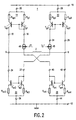
- Figure 2 shows an embodiment in which the first current mirror 14 and the second current mirror 22 comprise bipolar PNP transistors and the third current mirror 30 and the fourth current mirror 38 comprise bipolar NPN transistors.
- bipolar transistors may be replaced wholly or partly by unipolar MOS transistors.
- the control electrode, the first main electrode and the second main electrode correspond to the base, the emitter and the collector, respectively, for a bipolar transistor and to the gate, the source and the drain, respectively, for a unipolar transistor.
- the first current mirror 14 comprises a diode-connected PNP input transistor T ip1 , having its emitter connected to the first common current terminal 20 via an optional emitter resistor R ip1 and its collector to the first current input terminal 16, and a PNP output transistor T op1 , having its base connected to the base of the input transistor T ip1 , its emitter to the first common current terminal 20 via an optional emitter resistor R op1 and its collector to the first current output terminal 18.
- the optional emitter resistors improve the matching of the transistors and increase the thermal stability of the current mirror.
- the second current mirror 22 likewise comprises PNP transistors and the third current mirror 30 and the fourth current mirror 38 likewise comprise NPN transistors, the electrodes of the respective transistors being connected to the corresponding terminals of the current mirrors.
- the common-mode voltage of the write head 2 is completely indeterminate and may fluctuate with the data pattern of the information signal to be recorded. This is undesirable.
- the common-mode voltage should preferably lie halfway between the available output swing and should be independent of the signal content of the signal to be recorded. Since the write head 2 is arranged exclusively between high-impedance outputs of current mirrors it is possible to fix the common-mode voltage with a common-mode circuit.
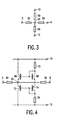
- Figure 3 shows a simple common-mode circuit.
- a series arrangement of a first resistor 50 connected between the first write terminal 6 and a first node 52, a second resistor 54 connected between the first node 52 and the second write terminal 8, a third resistor 56 connected between the first supply terminal 10 and the first node 52, and a fourth resistor 58 connected between the second supply terminal 12 and the first node 52 is arranged in parallel with the write head.
- the resistors 50 and 54 also function as damping resistors for the write head.
- the impedance at the first node 52 is dictated by the resistors 56 and 58. For a correct fixation of the common-mode voltage a minimal impedance is desired. However, the resistance value of the resistors 56 and 58 cannot be chosen arbitrarily small on account of the increasing current through these resistors.
- Figure 4 shows a common-mode circuit which mitigates this problem.
- the circuit again comprises a first resistor 60 connected between the first write terminal 6 and a first node 62, and a second resistor 64 connected between the first node 62 and the second write terminal 8 and, in addition, it comprises a first NPN transistor 66 having its emitter connected to the first node 62 and having its collector coupled to the first supply terminal 10, a diode-connected second NPN transistor 68 having its base connected to the base of the first NPN transistor 66, a third resistor 70 connected between the first supply terminal 10 and the collector of the second NPN transistor 68, a first PNP transistor 72 having its emitter connected to the first node 62 and having its collector coupled to the second supply terminal 12, a diode-connected second PNP transistor 74 having its base connected to the base of the first PNP transistor 72 and having its emitter connected to the emitter of the second NPN transistor 68, and a fourth resistor 76 connected between the second supply terminal 12 and the collector of the second P
- the circuit operates in class A/B. Seen at the first node 62, the impedance is low, which provides a correct fixation of the common-mode voltage.
- the class A/B operation enables a small quiescent current to be obtained in and a large maximum current to be supplied by the first NPN transistor 66 or the first PNP transistor 72.
- the effective common-mode resistance is equal to Rd/4, the resistance value of both the resistor 60 and the resistor 64 being equal to Rd/2.
- the overall damping resistance across the write head 2 is consequently Rd.
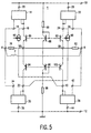
- FIG. 1 shows an embodiment in which this is implemented.
- the write amplifier 4 again comprises four current mirrors 14, 22, 30 and 38, the write head 2, the first switchable current source 46 and the second switchable current source 48 as shown in Figure 1.
- the common-mode circuit comprises a first resistor 78 connected between the first write terminal 6 and a first node 80, a second resistor 82 between a second node 84 and the second write terminal 8, a first transistor 86 of the NPN type having its emitter connected to the first node 80 and having its collector coupled to the first current input terminal 16, a diode-connected second transistor 88 of the NPN type having its base connected to the base of the first transistor 86, a third resistor 90 connected between the first supply terminal 10 and the collector of the second transistor 88, and a third transistor 92 of the NPN type having its base connected to the base of the first transistor 86 and its emitter to the second node 84 and having its collector coupled to the second current input terminal 24.
- the common-mode circuit further comprises a fourth transistor 94 of the PNP type having its emitter connected to the first node 80 and having its collector coupled to the third current input terminal 32, a diode-connected fifth transistor 96 of the PNP type having its base connected to the base of the fourth transistor 94 and having its emitter connected to the emitter of the second transistor 88, a fourth resistor 98 connected between the second supply terminal 12 and the collector of the fifth transistor 96, and a sixth transistor 100 of the PNP type having its base connected to the base of the fourth transistor 94 and its emitter to the second node 84 and having its collector coupled to the fourth current input terminal 40.
- the first node 80 and the second node 84 are interconnected.
- the quiescent current which flows through the transistors 86 and 94 now also flows into the first current input terminal 16 of the first current mirror 14 and into the third current input terminal 32 of the third current mirror 30.
- the quiescent current setting for the second current mirror 22 and the fourth current mirror 38 is obtained in a similar way by means of the transistors 92 and 100.
- the effective common-mode resistance is equal to Rd/(4(M+1)), where Rd/2 is the resistance value of the first resistor 78 and of the second resistor 82 and M is the current mirror ratio of the current mirrors 14, 22, 30 and 38.
- a voltage variation at the write terminal 6 produces in the first resistor 78 a current which appears M times as large at the same write terminal 6.
- the apparent resistance value Rd/2 of the first resistor 78 is thus reduced by a factor (M+1). The same occurs for the second resistor 82.
- the collector of the transistor 94 may be coupled to the fourth current input terminal 40 instead of to the third current input terminal 32 and that the collector of the transistor 100 may be coupled to the third current input terminal 32 instead of to the fourth current input terminal 40. This makes no difference for the quiescent current setting because the current in the transistors 94 and 100 is the same.
- the collectors of the transistors 86 and 92 may be connected crosswise to the current input terminal 16 and 24.
- Figure 6 shows an alternative solution, in which the connection between the first node 80 and the second node 84 is severed. Instead of this, a fifth resistor 102 is now connected between the write terminal 6 and the second node 84 and a sixth resistor 104 between the first node 80 and the write terminal 8.
- This solution can be more accurate because the transistors 86 and 92 as well as the transistors 94 and 100 now each see a separate degeneration resistor in series with their emitters. This mitigates the effect of a possible mismatch between the transistors 86 and 92 and between the transistors 94 and 100.
- the collector of the transistor 94 may be coupled to the fourth current input terminal 40 instead of to the third current input terminal 32 and that the collector of the transistor 100 may be coupled to the third current input terminal 32 instead of to the fourth current input terminal 40.
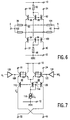
- FIG. 7 shows a circuit diagram of an implementation of the first switchable current source 46 and the second switchable current source 48 of the arrangements shown in Figures 1, 2 and 5.
- the two switchable current sources are united in one circuit comprising the following elements.
- An NPN transistor 106 having its base connected to a third node 108 and having its collector coupled to the first current input terminal 16
- an NPN transistor 110 having its base connected to the base of the transistor 106 and having its collector coupled to the first supply terminal 10
- a PNP transistor 112 having its base connected to a fourth node 114 and its emitter to the emitter of the transistor 106 and having its collector coupled to the fourth current input terminal 40
- a diode-connected PNP transistor 116 having its emitter connected to the emitter of the transistor 110 and having its base and its collector connected to the fourth node 114
- a bias current source 118 coupled to the fourth node 114 to supply a bias current I c to the fourth node 114.
- the circuit further comprises an NPN transistor 120 having its base connected to a fifth node 122 and having its collector coupled to the second current input terminal 24, an NPN transistor 124 having its base connected to the base of the transistor 120 and having its collector coupled to the first supply terminal 10, and a PNP transistor 126 having its base connected to the fourth node 114 and its emitter to the emitter of the transistor 120 and having its collector coupled to the third current input terminal 32.
- the nodes 108 and 122 are driven in phase opposition with the information signal U i and the inverse information signal NU i via buffers 128 and 130.
- the transistor 110 When the voltage at the node 108 is high and the voltage at the node 122 is low the transistor 110 is conductive and the transistor 124 is cut off.
- the bias current I c of the bias current source 118 flows wholly through the transistor 110 via the transistor 116.
- the base-emitter junctions of the transistors 106, 110, 116 and 112 form a translinear loop, the sum of the base-emitter voltages of the transistors 106 and 112 being equal to the sum of the base-emitter voltages of the transistors 110 and 116.
- SQRT is the root function
- M the ratio between the emitter areas of the transistors 106 and 110
- N the ratio between the emitter areas of the transistors 112 and 116.
- a current I will flow between the terminals 16 and 40, whose magnitude is proportional to the current I c , the proportionality factor being determined by the geometries of the transistors 106, 110, 112 and 116.
- the bias current source 118 is preferably an adjustable or programmable current source, for example an IDAC (digital-to-analog converter with current output). Since the current input terminals 16, 24, 32 and 40 are all coupled to collectors the d.c. level of the information signals U i and NU i is now isolated from the d.c. levels of the current input terminals of the current mirrors of the write amplifier. Thus, the switched current sources 46 and 48 are floating relative to the supply voltages at the first supply terminal 10 and the second supply terminal 12.
- IDAC digital-to-analog converter with current output
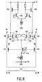
- the buffers 128 and 130 may comprise emitter-followers with emitter current sources. However, saving current is possible by using the currents through the transistors 110 and 124 for this purpose. Figure 8 shows how this can be realised.
- the buffer 128 is now an NPN emitter-follower 132 whose base receives an amplified information signal, whose emitter is connected to the third node 108 and whose collector is coupled to the first supply terminal 10.
- the collector of the transistor 110 is connected to the emitter of the emitter-follower 132.
- the buffer 130 likewise comprises an NPN emitter-follower 134 whose base receives an amplified inverse information signal, whose emitter is connected to the fifth node 122 and whose collector is coupled to the first supply terminal 10.
- the collector of the transistor 124 is connected to the emitter of the emitter-follower 134.
- the collector currents of the transistors 110 and 124 consequently also flow through the emitter-followers 132 and 134, respectively.
- an NPN transistor 136 having its base connected to the base of the transistor 110 and its emitter to the emitter of the transistor 110 and having its collector coupled to the fifth node 122
- an NPN transistor 138 having its base connected to the base of the transistor 124 and its emitter to the emitter of the transistor 124 and having its collector coupled to the third node 108.
- the transistors 136 and 138 ensure that the currents through the emitter-followers 132 and 134 cannot become zero if one of the transistors 110 and 124 is cut off.
- each of the two emitter-followers always receives half the bias current I c if the geometries of the transistors 110, 136, 138 and 124 are selected to be equal.
- the bases of the emitter-followers 132 and 134 are driven, by way of example, by the transistors of a differential pair 140 whose bases are arranged to receive the complementary information signals U i and NU i , which are supplied, for example, by a data flip-flop.
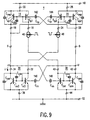
- Figure 9 again shows the arrangement of Figure 2 but now without the write head 2 and the emitter resistors in the current mirrors.
- a number of parasitic capacitances are shown, i.e. one having a value C cwp between collector and well of the PNP output transistors T op1 and T op2 , one having a value C csn between collector and substrate of the NPN output transistors T on3 and T on4 , one having a value C cbp between collector and base of the PNP output transistors T op1 and T op2 , and one having a value C cbn between collector and base of the NPN output transistors T on3 and T on4 .
- All these parasitic capacitances have an effect on the write current through the write terminals 6 and 8.
- the effect is that at high frequencies the write current flows through the parasitic capacitances instead of through the write head. This effect limits the bit rate of the write current.
- four neutralising capacitors 142, 144, 146 and 148 are provided, whose capacitance values are C np , C nn and C nn , respectively.
- the capacitor 142 is connected between the first current input terminal 16 and the second current output terminal 26, the second capacitor 144 between the second current input terminal 24 and the first current output terminal 18, the third capacitor 146 between the third current input terminal 32 and the fourth current output terminal 42, and the fourth capacitor 148 between the fourth current input terminal 40 and the third current output terminal.
- C h (C cwp +C csn +(1+M)(C cbp +C cbn ) + (1-M)(C np +C nn ))/2
- C h (C cwp +C csn +(1+M)(C cbp +C cbn ) + (1-M)(C np +C nn ))/2
- the current through the capacitor 146 has an opposite sign and is enlarged by the current mirror factor M. A similar calculation applies to the other current output terminals.
Landscapes
- Digital Magnetic Recording (AREA)
- Electronic Switches (AREA)
- Magnetic Record Carriers (AREA)
- Signal Processing For Digital Recording And Reproducing (AREA)
Claims (11)
- Anordnung zum Aufzeichnen eines Informationssignals auf einem magnetischen Aufzeichnungsträger, mit einem Schreibkopf (2) zum Aufzeichnen von Informationen auf dem Aufzeichnungsträger und einem Schreibverstärker (4) zum Ansteuern des Schreibkopfes (2) in Reaktion auf das Informationssignal, wobei der Schreibverstärker (4) umfasst: eine erste Schreibklemme (6) und eine zweite Schreibklemme (8), die mit dem Schreibkopf (2) gekoppelt sind;gekennzeichnet durcheine erste Speiseklemme (10) und eine zweite Speiseklemme (12) zum Anschluss einer Speisespannung für den Schreibverstärker (4);einen ersten Stromspiegel (14) mit einer ersten Stromeingangsklemme (16), einer ersten mit der ersten Schreibklemme (6) gekoppelten Stromausgangsklemme (18) und einer mit der ersten Speiseklemme (10) verbundenen ersten gemeinsamen Stromklemme (20);einen zweiten Stromspiegel (22) mit einer zweiten Stromeingangsklemme (24), einer zweiten mit der zweiten Schreibklemme (8) gekoppelten Stromausgangsklemme (26) und einer mit der ersten Speiseklemme (10) verbundenen zweiten gemeinsamen Stromklemme (28); eine mit der ersten Stromeingangsklemme (16) verbundene erste schaltbare Stromquelle (46) zum Liefern eines ersten Stromes für einen ersten Wert des Informationssignals;eine mit der zweiten Stromeingangsklemme (24) verbundene zweite schaltbare Stromquelle (48) zum Liefern eines zweiten Stromes für einen zweiten Wert des Informationssignals; dritte (30) und vierte (38) Stromspiegel, deren Ausgangsströme mit dem ersten und dem zweiten Strom der genannten ersten (46) und zweiten (48) schaltbaren Stromquelle gespiegelt werden und jeweils zu der ersten (6) und zweiten (8) Schreibklemme fließende Ströme bestimmen,um bei einem ersten Wert des Informationssignals über die erste Schreibklemme (6) unddie zweite Schreibklemme (8) einen Strompfad zwischen der ersten Stromausgangsklemme (18) und der zweiten Speiseklemme (12) herzustellen und um bei einem zweiten Wert des Informationssignals über die erste Schreibklemme (6) und die zweite Schreibklemme (8) einen Strompfad zwischen der zweiten Stromausgangsklemme (18) und der zweiten Speiseklemme (12) herzustellen,den genannten dritten Stromspiegel (30), mit einer dritten Stromeingangsklemme (32), einer mit der ersten Schreibklemme (6) gekoppelten dritten Stromausgangsklemme (34) und einer mit der zweiten Speiseklemme (12) verbundenen dritten gemeinsamen Stromklemme (36);den genannten vierten Stromspiegel (38), mit einer vierten Stromeingangsklemme (40), einer mit der zweiten Schreibklemme (8) gekoppelten vierten Stromausgangsklemme (42) und einer mit der zweiten Speiseklemme (12) verbundenen vierten gemeinsamen Stromklemme (44);wobei die genannte erste schaltbare Stromquelle (46) zwischen die erste Stromeingangsklemme (16) und die vierte Stromeingangsklemme (40) geschaltet ist unddie genannte zweite schaltbare Stromquelle (48) zwischen die zweite Stromeingangsklemme (24) und die dritte Stromeingangsklemme (32) geschaltet ist.
- Anordnung nach Anspruch 1, dadurch gekennzeichnet, dass der Schreibverstärker (4) weiterhin umfasst: einen zwischen die erste Schreibklemme (6) und einen ersten Knotenpunkt (52) geschalteten ersten Widerstand (50), einen zwischen den ersten Knotenpunkt (52) und die zweite Schreibklemme (8) geschalteten zweiten Widerstand (54), einen zwischen die erste Speiseklemme (10) und den ersten Knotenpunkt (52) geschalteten dritten Widerstand (56), und einen zwischen die zweite Speiseklemme (12) und den ersten Knotenpunkt (52) geschalteten vierten Widerstand (58).
- Anordnung nach Anspruch 1, dadurch gekennzeichnet, dass der Schreibverstärker weiterhin umfasst: einen zwischen die erste Schreibklemme (6) und einen ersten Knotenpunkt (62) geschalteten ersten Widerstand (60), einen zwischen den ersten Knotenpunkt (62) und die zweite Schreibklemme (8) geschalteten zweiten Widerstand (64), einen ersten Transistor (66) eines ersten Leitungstyps mit einer Steuerelektrode, einer mit dem ersten Knotenpunkt (62) verbundenen ersten Hauptelektrode und einer mit der ersten Speiseklemme (10) gekoppelten zweiten Hauptelektrode, einen zweiten Transistor (68) des ersten Leitungstyps mit einer mit der Steuerelektrode des ersten Transistors (66) verbundenen Steuerelektrode, einer ersten Hauptelektrode und einer mit der Steuerelektrode des zweiten Transistors (68) verbundenen zweiten Hauptelektrode, einen zwischen die erste Speiseklemme (10) und die zweite Hauptelektrode des zweiten Transistors (68) geschalteten dritten Widerstand (70), einen dritten Transistor (72) eines zweiten Leitungstyps mit einer Steuerelektrode, einer mit dem ersten Knotenpunkt (62) verbundenen ersten Hauptelektrode und einer mit der zweiten Speiseklemme (12) gekoppelten zweiten Hauptelektrode, einen vierten Transistor (74) des zweiten Leitungstyps mit einer mit der Steuerelektrode des dritten Transistors (72) verbundenen Steuerelektrode, einer mit der ersten Hauptelektrode des zweiten Transistors (68) verbundenen ersten Hauptelektrode und einer mit der Steuerelektrode des vierten Transistors (74) verbundenen zweiten Hauptelektrode und einen zwischen die zweite Speiseklemme (12) und die zweite Hauptelektrode des vierten Transistors (74) geschalteten vierten Widerstand (76).
- Anordnung nach Anspruch 1, dadurch gekennzeichnet, dass der Schreibverstärker weiterhin umfasst:einen zwischen die erste Schreibklemme (6) und einen ersten Knotenpunkt (80) geschalteten ersten Widerstand (78), einen zwischen den ersten Knotenpunkt (80) und die zweite Schreibklemme (8) geschalteten zweiten Widerstand (104), einen zwischen die erste Schreibklemme (6) und einen zweiten Knotenpunkt (84) geschalteten dritten Widerstand (102), einen zwischen den zweiten Knotenpunkt (84) und die zweite Schreibklemme (8) geschalteten vierten Widerstand (82),einen ersten Transistor (86) eines ersten Leitungstyps mit einer Steuerelektrode, einer mit dem ersten Knotenpunkt (80) verbundenen ersten Hauptelektrode und einer mit der ersten Stromeingangsklemme (16) gekoppelten zweiten Hauptelektrode, einen zweiten Transistor (88) des ersten Leitungstyps mit einer mit der Steuerelektrode des ersten Transistors (86) verbundenen Steuerelektrode, einer ersten Hauptelektrode und einer mit der Steuerelektrode des zweiten Transistors (88) verbundenen zweiten Hauptelektrode, einen zwischen die erste Speiseklemme (10) und die zweite Hauptelektrode des zweiten Transistors (88) geschalteten fünften Widerstand (90), einen dritten Transistor (92) des ersten Leitungstyps mit einer mit der Steuerelektrode des ersten Transistors (86) verbundenen Steuerelektrode, einer mit dem zweiten Knotenpunkt (84) verbundenen ersten Hauptelektrode und einer mit der zweiten Stromeingangsklemme (24) gekoppelten zweiten Hauptelektrode,einen vierten Transistor (94) eines zweiten Leitungstyps mit einer Steuerelektrode, einer mit dem ersten Knotenpunkt (80) verbundenen ersten Hauptelektrode und einer mit einer der dritten Stromeingangsklemme (32) und der vierten Stromeingangsklemme (40) gekoppelten zweiten Hauptelektrode, einen fünften Transistor (96) des zweiten Leitungstyps mit einer mit der Steuerelektrode des vierten Transistors (94) verbundenen Steuerelektrode, einer mit der ersten Hauptelektrode des zweiten Transistors (88) gekoppelten ersten Hauptelektrode und einer mit der Steuerelektrode des fünften Transistors (96) verbundenen zweiten Hauptelektrode, einen zwischen die zweite Speiseklemme (12) und die zweite Hauptelektrode des fünften Transistors (96) geschalteten sechsten Widerstand (98), einen sechsten Transistor (100) des zweiten Leitungstyps mit einer mit der Steuerelektrode des vierten Transistors (94) verbundenen Steuerelektrode, einer mit dem zweiten Knotenpunkt (84) verbundenen ersten Hauptelektrode und einer mit der anderen der dritten Stromeingangsklemme (32) und der vierten Stromeingangsklemme (40) gekoppelten zweiten Hauptelektrode.
- Anordnung nach Anspruch 4, dadurch gekennzeichnet, dass der zweite Knotenpunkt (84) mit dem ersten Knotenpunkt (80) verbunden ist.
- Anordnung nach Anspruch 1, 2, 3, 4, oder 5, dadurch gekennzeichnet, dass die erste (46) und die zweite (48) schaltbare Stromquelle umfassen:einen siebten Transistor (106) eines ersten Leitungstyps mit einer mit einem dritten Knotenpunkt (108) verbundenen Steuerelektrode, einer ersten Hauptelektrode, und einer mit der ersten Stromeingangsklemme (16) gekoppelten zweiten Hauptelektrode, einen achten Transistor (110) des ersten Leitungstyps mit einer mit der Steuerelektrode des siebten Transistors (106) gekoppelten Steuerelektrode, einer ersten Hauptelektrode, und einer mit der ersten Speiseklemme (10) gekoppelten zweiten Hauptelektrode,einen neunten Transistor (112) eines zweiten Leitungstyps mit einer mit einem vierten Knotenpunkt (114) verbundenen Steuerelektrode, einer mit der ersten Hauptelektrode des siebten Transistors (106) verbundenen ersten Hauptelektrode und einer mit der vierten Stromeingangsklemme (40) gekoppelten zweiten Hauptelektrode, einen als Diode geschalteten zehnten Transistor (116) des zweiten Leitungstyps mit einer mit der ersten Hauptelektrode des achten Transistors (110) verbundenen ersten Hauptelektrode und mit einer Steuerelektrode und zweiten Hauptelektrode, die mit dem vierten Knotenpunkt (114) verbunden sindeine mit dem vierten Knotenpunkt (114) gekoppelte Eingangsruhestromquelle (118) zum Liefern eines Eingangsruhestroms an den vierten Knotenpunkt (114),einen elften Transistor (120) des ersten Leitungstyps mit einer mit einem fünften Knotenpunkt (122) verbundenen Steuerelektrode, einer ersten Hauptelektrode und einer mit der zweiten Stromeingangsklemme (24) gekoppelten zweiten Hauptelektrode, einen zwölften Transistor (124) des ersten Leitungstyps mit einer mit der Steuerelektrode des elften Transistors (120) verbundenen Steuerelektrode, einer ersten Hauptelektrode und einer mit der ersten Speiseklemme (10) gekoppelten zweiten Hauptelektrode, und einen dreizehnten Transistor (126) des zweiten Leitungstyps mit einer mit dem vierten Knotenpunkt (114) verbundenen Steuerelektrode, einer mit der ersten Hauptelektrode des Transistors (120) verbundenen ersten Hauptelektrode und einer mit der dritten Stromeingangsklemme (32) gekoppelten zweiten Hauptelektrode.
- Anordnung nach Anspruch 6, dadurch gekennzeichnet, dass die erste (46) und die zweite (48) schaltbare Stromquelle weiterhin umfassen:einen vierzehnten Transistor (132) des ersten Leitungstyps mit einer Steuerelektrode zum Empfangen des Informationssignals, einer mit dem dritten Knotenpunkt (108) verbundenen ersten Hauptelektrode und einer mit der ersten Speiseklemme (10) gekoppelten zweiten Hauptelektrode, einen fünfzehnten Transistor (134) des ersten Leitungstyps mit einer Steuerelektrode zum Empfangen des Informationssignals, einer mit dem fünften Knotenpunkt (122) verbundenen ersten Hauptelektrode und einer mit der ersten Speiseklemme (10) gekoppelten zweiten Hauptelektrode, einen sechzehnten Transistor (136) des ersten Leitungstyps mit einer mit der Steuerelektrode des achten Transistors (110) verbundenen Steuerelektrode, einer mit der ersten Hauptelektrode des achten Transistors (110) verbundenen ersten Hauptelektrode und einer mit dem fünften Knotenpunkt (122) gekoppelten zweiten Hauptelektrode, einen siebzehnten Transistor (138) des ersten Leitungstyps mit einer mit der Steuerelektrode des zwölften Transistors (124) verbundenen Steuerelektrode, einer mit der ersten Hauptelektrode des zwölften Transistors (124) verbundenen ersten Hauptelektrode und einer mit dem dritten Knotenpunkt (108) gekoppelten zweiten Hauptelektrode, wobei die zweite Hauptelektrode des achten Transistors (110) mit dem dritten Knotenpunkt (108) verbunden ist und die zweite Hauptelektrode des zwölften Transistors (124) mit dem fünften Knotenpunkt (122) verbunden ist.
- Anordnung nach Anspruch 1, 2, 3, 4, 5, 6 oder 7, dadurch gekennzeichnet, dass der Schreibverstärker (4) weiterhin zumindest eines der folgenden umfasst:einen zwischen die erste Stromeingangsklemme (16) und die zweite Stromausgangsklemme (26) geschalteten ersten Kondensator (142), einen zwischen die zweite Stromeingangsklemme (24) und die erste Stromausgangsklemme (18) geschalteten zweiten Kondensator (144), einen zwischen die dritte Stromeingangsklemme (32) und die vierte Stromausgangsklemme (42) geschalteten dritten Kondensator (146) und einen zwischen die vierte Stromeingangsklemme (40) und die dritte Stromausgangsklemme (34) geschalteten vierten Kondensator (148).
- Anordnung nach Anspruch 1, 2, 3, 4, 5, 6, 7 oder 8, dadurch gekennzeichnet, dass der dritte Stromspiegel (30) und der vierte Stromspiegel (38) jeweils einen als Diode geschalteten Eingangstransistor (Tin) eines ersten Leitungstyps mit einer Steuerelektrode und einer mit der dritten (32) bzw. der vierten (40) Stromeingangsklemme verbundenen zweiten Hauptelektrode und mit einer mit der zweiten Speiseklemme (12) gekoppelten ersten Hauptelektrode umfassen sowie einen Ausgangstransistor (Ton) des ersten Leitungstyps mit einer mit der Steuerelektrode des betreffenden Eingangstransistors (Tin) verbundenen Steuerelektrode, einer mit der zweiten Speiseklemme (12) gekoppelten ersten Hauptelektrode und einer mit der dritten (34) und der vierten (42) Stromausgangsklemme gekoppelten zweiten Hauptelektrode, und dassder erste Stromspiegel (14) und der zweite Stromspiegel (22) jeweils einen als Diode geschalteten Eingangstransistor (Tip) eines zweiten Leitungstyps mit einer Steuerelektrode und einer mit der ersten (16) bzw. der zweiten (24) Stromeingangsklemme verbundenen zweiten Hauptelektrode und mit einer mit der ersten Speiseklemme (10) gekoppelten ersten Hauptelektrode umfassen sowie einen Ausgangstransistor (Top) des zweiten Leitungstyps mit einer mit der Steuerelektrode des betreffenden Eingangstransistors (Tip) verbundenen Steuerelektrode, einer mit der ersten Speiseklemme (10) gekoppelten ersten Hauptelektrode und einer mit der ersten (18) und der zweiten (26) Stromausgangsklemme verbundenen zweiten Hauptelektrode.
- Anordnung nach Anspruch 9, dadurch gekennzeichnet, dass die ersten Hauptelektroden der Eingangstransistoren (Tip) und Ausgangstransistoren (Top) des ersten (14) und des zweiten (22) Stromspiegels mit der ersten Speiseklemme (10) über Widerstände (Rip, Rop) verbunden sind, und die ersten Hauptelektroden der Eingangstransistoren (Tin) und Ausgangstransistoren (Ton) des dritten (30) und des vierten (38) Stromspiegels mit der zweiten Speiseklemme (12) über Widerstände (Rin, Ron) verbunden sind.
- Schreibverstärker (4) zum Ansteuern eines Schreibkopfes (2) in Reaktion auf ein Informationssignal, wobei der Schreibverstärker (4) umfasst: eine erste Schreibklemme (6) und eine zweite Schreibklemme (8) zum Koppeln mit dem Schreibkopf (2); eine erste Speiseklemme (10) und eine zweite Speiseklemme (12) zum Anschluss einer Speisespannung für den Schreibverstärker (4);gekennzeichnet durcheinen ersten Stromspiegel (14) mit einer ersten Stromeingangsklemme (16), einer ersten mit der ersten Schreibklemme (6) gekoppelten Stromausgangsklemme (18) und einer mit der ersten Speiseklemme (10) verbundenen ersten gemeinsamen Stromklemme (20);einen zweiten Stromspiegel (22) mit einer zweiten Stromeingangsklemme (24), einer zweiten mit der zweiten Schreibklemme (8) gekoppelten Stromausgangsklemme (26) und einer mit der ersten Speiseklemme (10) verbundenen zweiten gemeinsamen Stromklemme (28)eine mit der ersten Stromeingangsklemme (16) verbundene erste schaltbare Stromquelle (46) zum Liefern eines ersten Stromes für einen ersten Wert des Informationssignals;eine mit der zweiten Stromeingangsklemme (24) verbundene zweite schaltbare Stromquelle (48) zum Liefern eines zweiten Stromes für einen zweiten Wert des Informationssignals; dritte (30) und vierte (38) Stromspiegel, deren Ausgangsströme mit dem ersten und dem zweiten Strom der genannten ersten (46) und zweiten (48) schaltbaren Stromquelle gespiegelt werden und jeweils zu der ersten (6) und zweiten (8) Schreibklemme fließende Ströme bestimmen,um bei einem ersten Wert des Informationssignals über die erste Schreibklemme (6) unddie zweite Schreibklemme (8) einen Strompfad zwischen der ersten Stromausgangsklemme (18) und der zweiten Speiseklemme (12) herzustellen und um bei einem zweiten Wert des Informationssignals über die erste Schreibklemme (6) und die zweite Schreibklemme (8) einen Strompfad zwischen der zweiten Stromausgangsklemme (18) und der zweiten Speiseklemme (12) herzustellen,den genannten dritten Stromspiegel (30), mit einer dritten Stromeingangsklemme (32), einer mit der ersten Schreibklemme (6) gekoppelten dritten Stromausgangsklemme (34) und einer mit der zweiten Speiseklemme (12) verbundenen dritten gemeinsamen Stromklemme (36);den genannten vierten Stromspiegel (38) mit einer vierten Stromeingangsklemme (40), einer mit der zweiten Schreibklemme (8) gekoppelten vierten Stromausgangsklemme (42) und einer mit der zweiten Speiseklemme (12) verbundenen vierten gemeinsamen Stromklemme (44);wobei die genannte erste schaltbare Stromquelle (46) zwischen die erste Stromeingangsklemme (16) und die vierte Stromeingangsklemme (40) geschaltet ist unddie genannte zweite schaltbare Stromquelle (48) zwischen die zweite Stromeingangsklemme (24) und die dritte Stromeingangsklemme (32) geschaltet ist.
Priority Applications (1)
| Application Number | Priority Date | Filing Date | Title |
|---|---|---|---|
| EP95918712A EP0764321B1 (de) | 1994-06-10 | 1995-06-06 | Anordnung zur aufzeichnung eines informationssignals auf einen magnetaufzeichnungsträger |
Applications Claiming Priority (4)
| Application Number | Priority Date | Filing Date | Title |
|---|---|---|---|
| EP94201660 | 1994-06-10 | ||
| EP94201660 | 1994-06-10 | ||
| PCT/IB1995/000435 WO1995035564A2 (en) | 1994-06-10 | 1995-06-06 | Arrangement for recording an information signal on a magnetic record carrier |
| EP95918712A EP0764321B1 (de) | 1994-06-10 | 1995-06-06 | Anordnung zur aufzeichnung eines informationssignals auf einen magnetaufzeichnungsträger |
Publications (2)
| Publication Number | Publication Date |
|---|---|
| EP0764321A2 EP0764321A2 (de) | 1997-03-26 |
| EP0764321B1 true EP0764321B1 (de) | 2001-11-28 |
Family
ID=8216940
Family Applications (1)
| Application Number | Title | Priority Date | Filing Date |
|---|---|---|---|
| EP95918712A Expired - Lifetime EP0764321B1 (de) | 1994-06-10 | 1995-06-06 | Anordnung zur aufzeichnung eines informationssignals auf einen magnetaufzeichnungsträger |
Country Status (7)
| Country | Link |
|---|---|
| US (1) | US5668676A (de) |
| EP (1) | EP0764321B1 (de) |
| JP (1) | JP3623963B2 (de) |
| KR (1) | KR100376024B1 (de) |
| AT (1) | ATE209815T1 (de) |
| DE (1) | DE69524219T2 (de) |
| WO (1) | WO1995035564A2 (de) |
Families Citing this family (15)
| Publication number | Priority date | Publication date | Assignee | Title |
|---|---|---|---|---|
| CN1148723C (zh) * | 1995-11-21 | 2004-05-05 | 皇家菲利浦电子有限公司 | 包括磁写入头和具有电容前馈补偿的写入放大器的装置 |
| JP2002516447A (ja) | 1998-05-19 | 2002-06-04 | コーニンクレッカ フィリップス エレクトロニクス エヌ ヴィ | 書き込み駆動回路を具備する記録装置 |
| US6222695B1 (en) | 1998-08-10 | 2001-04-24 | Siemens Microelectronics, Inc. | System and method for a preamplifier write circuit with reduced rise/fall time |
| US6366421B2 (en) * | 1998-12-17 | 2002-04-02 | Texas Instruments Incorporated | Adjustable writer overshoot for a hard disk drive write head |
| US6307695B1 (en) * | 1999-03-15 | 2001-10-23 | Philips Electronics North America Corporation | Magnetic disk write channel with damping network |
| EP1110211A1 (de) * | 1999-06-22 | 2001-06-27 | Koninklijke Philips Electronics N.V. | Schreibtreiber |
| US6275092B1 (en) * | 1999-11-16 | 2001-08-14 | Texas Instruments Incorporated | Active damping circuit |
| US6512649B1 (en) * | 2000-08-30 | 2003-01-28 | Stmicroelectronics, Inc. | Method for differentially writing to a memory disk |
| US6970316B2 (en) * | 2001-11-09 | 2005-11-29 | Stmicroelectronics, Inc. | Write head driver circuit and method for writing to a memory disk |
| US7119990B2 (en) | 2002-05-30 | 2006-10-10 | Komag, Inc. | Storage device including a center tapped write transducer |
| US6857937B2 (en) * | 2002-05-30 | 2005-02-22 | Komag, Inc. | Lapping a head while powered up to eliminate expansion of the head due to heating |
| US7006313B2 (en) * | 2002-06-25 | 2006-02-28 | Texas Instruments Incorporated | Circuit and method to match common mode flex impedance and to achieve symmetrical switching voltage outputs of write driver |
| US7133234B2 (en) * | 2003-07-08 | 2006-11-07 | Texas Instruments Incorporated | Hard disk drive preamplifier write driver |
| US7184232B2 (en) * | 2003-09-18 | 2007-02-27 | Texas Instruments Incorporated | Apparatus and method for driving a write head |
| US7701654B2 (en) * | 2005-09-23 | 2010-04-20 | Agere Systems Inc. | Apparatus and method for controlling common mode voltage of a disk drive write head |
Family Cites Families (4)
| Publication number | Priority date | Publication date | Assignee | Title |
|---|---|---|---|---|
| US4551772A (en) * | 1984-03-28 | 1985-11-05 | Storage Technology Corporation | Write drive with current mirrors which reduce feed-through |
| US5287231A (en) * | 1992-10-06 | 1994-02-15 | Vtc Inc. | Write circuit having current mirrors between predriver and write driver circuits for maximum head voltage swing |
| US5296975A (en) * | 1992-10-09 | 1994-03-22 | International Business Machines Corporation | High-transition-rate, low-supply-voltage write driver circuitry for magnetic inductive write head |
| US5386328A (en) * | 1993-06-18 | 1995-01-31 | Silicon Systems, Inc. | Current mirror based write driver |
-
1995
- 1995-06-06 KR KR1019960707155A patent/KR100376024B1/ko not_active Expired - Fee Related
- 1995-06-06 EP EP95918712A patent/EP0764321B1/de not_active Expired - Lifetime
- 1995-06-06 JP JP50188296A patent/JP3623963B2/ja not_active Expired - Lifetime
- 1995-06-06 DE DE69524219T patent/DE69524219T2/de not_active Expired - Fee Related
- 1995-06-06 WO PCT/IB1995/000435 patent/WO1995035564A2/en not_active Ceased
- 1995-06-06 AT AT95918712T patent/ATE209815T1/de not_active IP Right Cessation
- 1995-06-09 US US08/489,191 patent/US5668676A/en not_active Expired - Fee Related
Also Published As
| Publication number | Publication date |
|---|---|
| DE69524219T2 (de) | 2002-08-14 |
| ATE209815T1 (de) | 2001-12-15 |
| JPH10501646A (ja) | 1998-02-10 |
| WO1995035564A3 (en) | 1996-02-15 |
| DE69524219D1 (de) | 2002-01-10 |
| WO1995035564A2 (en) | 1995-12-28 |
| EP0764321A2 (de) | 1997-03-26 |
| HK1013166A1 (en) | 1999-08-13 |
| JP3623963B2 (ja) | 2005-02-23 |
| US5668676A (en) | 1997-09-16 |
| KR100376024B1 (ko) | 2003-08-14 |
Similar Documents
| Publication | Publication Date | Title |
|---|---|---|
| EP0804789B1 (de) | Anordnung mit einem magnetschreibkopf und schreibverstärker mit kapazitiver, vorwärtsgekoppelter kompensation | |
| EP0764321B1 (de) | Anordnung zur aufzeichnung eines informationssignals auf einen magnetaufzeichnungsträger | |
| EP0764320B1 (de) | Anordnung mit magnetschreibkopf sowie schreibverstärker mit kapazitiver stromkompensation | |
| JP3514461B2 (ja) | 情報読み出し装置 | |
| US7206155B2 (en) | High-speed, low power preamplifier write driver | |
| JPH08504290A (ja) | 記録担体上のトラックから情報を読み出す装置 | |
| US7068454B2 (en) | Hard disk storage system including a first transistor type and a second transistor type where a first voltage level pulls one of a first pair of transistors and a second voltage level pulls one of a second pair of transistors at substantially the same time | |
| JP2000339608A (ja) | 改善された、スイッチング特性、同相モード電圧、とヘッド電流制御を持つ書き込み増幅器 | |
| US6150876A (en) | Voltage bias, current sense preamplifier for a magnetoresistive reader | |
| US6107873A (en) | Low noise common-emitter preamplifier for magneto-resistive heads | |
| KR100634130B1 (ko) | 기록 구동회로를 구비한 레코딩 장치 | |
| US5739706A (en) | Magnetically recording apparatus | |
| JP3516178B2 (ja) | プリアンプ回路装置 | |
| HK1013166B (en) | Arrangement for recording an information signal on a magnetic record carrier | |
| HK1013164B (en) | Arrangement comprising a magnetic write head, and write amplifier with capacitive current compensation | |
| JPS60254922A (ja) | 双対モ−ド論理回路 | |
| KR900002251B1 (ko) | 디지탈 자기 기록 회로 | |
| US5680268A (en) | Apparatus for magnetic recording and playback having a recording/playback coil split by a center tap and supplying an unbalanced write current | |
| JP2779432B2 (ja) | リード/ライト用集積回路 | |
| JPH0359805A (ja) | デジタル磁気記録回路 | |
| US20050259344A1 (en) | High output impedance biasing for magnetoresistive elements | |
| JPH0626001U (ja) | 磁気記録再生回路 | |
| JPS616983A (ja) | 直流再生回路 | |
| JPH04307403A (ja) | フレキシブルディスク装置のリード/ライト回路 |
Legal Events
| Date | Code | Title | Description |
|---|---|---|---|
| PUAI | Public reference made under article 153(3) epc to a published international application that has entered the european phase |
Free format text: ORIGINAL CODE: 0009012 |
|
| 17P | Request for examination filed |
Effective date: 19970110 |
|
| AK | Designated contracting states |
Kind code of ref document: A2 Designated state(s): AT BE DE FR GB |
|
| RAP3 | Party data changed (applicant data changed or rights of an application transferred) |
Owner name: KONINKLIJKE PHILIPS ELECTRONICS N.V. |
|
| 17Q | First examination report despatched |
Effective date: 19990729 |
|
| GRAG | Despatch of communication of intention to grant |
Free format text: ORIGINAL CODE: EPIDOS AGRA |
|
| GRAG | Despatch of communication of intention to grant |
Free format text: ORIGINAL CODE: EPIDOS AGRA |
|
| GRAH | Despatch of communication of intention to grant a patent |
Free format text: ORIGINAL CODE: EPIDOS IGRA |
|
| GRAH | Despatch of communication of intention to grant a patent |
Free format text: ORIGINAL CODE: EPIDOS IGRA |
|
| GRAA | (expected) grant |
Free format text: ORIGINAL CODE: 0009210 |
|
| AK | Designated contracting states |
Kind code of ref document: B1 Designated state(s): AT BE DE FR GB |
|
| PG25 | Lapsed in a contracting state [announced via postgrant information from national office to epo] |
Ref country code: BE Free format text: LAPSE BECAUSE OF FAILURE TO SUBMIT A TRANSLATION OF THE DESCRIPTION OR TO PAY THE FEE WITHIN THE PRESCRIBED TIME-LIMIT Effective date: 20011128 Ref country code: AT Free format text: LAPSE BECAUSE OF FAILURE TO SUBMIT A TRANSLATION OF THE DESCRIPTION OR TO PAY THE FEE WITHIN THE PRESCRIBED TIME-LIMIT Effective date: 20011128 |
|
| REF | Corresponds to: |
Ref document number: 209815 Country of ref document: AT Date of ref document: 20011215 Kind code of ref document: T |
|
| REG | Reference to a national code |
Ref country code: GB Ref legal event code: IF02 |
|
| REF | Corresponds to: |
Ref document number: 69524219 Country of ref document: DE Date of ref document: 20020110 |
|
| PLBE | No opposition filed within time limit |
Free format text: ORIGINAL CODE: 0009261 |
|
| STAA | Information on the status of an ep patent application or granted ep patent |
Free format text: STATUS: NO OPPOSITION FILED WITHIN TIME LIMIT |
|
| 26N | No opposition filed | ||
| REG | Reference to a national code |
Ref country code: GB Ref legal event code: 746 Effective date: 20050518 |
|
| PGFP | Annual fee paid to national office [announced via postgrant information from national office to epo] |
Ref country code: DE Payment date: 20080808 Year of fee payment: 14 |
|
| PGFP | Annual fee paid to national office [announced via postgrant information from national office to epo] |
Ref country code: FR Payment date: 20080626 Year of fee payment: 14 |
|
| REG | Reference to a national code |
Ref country code: FR Ref legal event code: ST Effective date: 20100226 |
|
| PG25 | Lapsed in a contracting state [announced via postgrant information from national office to epo] |
Ref country code: FR Free format text: LAPSE BECAUSE OF NON-PAYMENT OF DUE FEES Effective date: 20090630 |
|
| PG25 | Lapsed in a contracting state [announced via postgrant information from national office to epo] |
Ref country code: DE Free format text: LAPSE BECAUSE OF NON-PAYMENT OF DUE FEES Effective date: 20100101 |
|
| PGFP | Annual fee paid to national office [announced via postgrant information from national office to epo] |
Ref country code: GB Payment date: 20110630 Year of fee payment: 17 |
|
| GBPC | Gb: european patent ceased through non-payment of renewal fee |
Effective date: 20120606 |
|
| PG25 | Lapsed in a contracting state [announced via postgrant information from national office to epo] |
Ref country code: GB Free format text: LAPSE BECAUSE OF NON-PAYMENT OF DUE FEES Effective date: 20120606 |