EP0943931A2 - Bilderzeugungsapparat - Google Patents
Bilderzeugungsapparat Download PDFInfo
- Publication number
- EP0943931A2 EP0943931A2 EP99301982A EP99301982A EP0943931A2 EP 0943931 A2 EP0943931 A2 EP 0943931A2 EP 99301982 A EP99301982 A EP 99301982A EP 99301982 A EP99301982 A EP 99301982A EP 0943931 A2 EP0943931 A2 EP 0943931A2
- Authority
- EP
- European Patent Office
- Prior art keywords
- imaging apparatus
- transfer elements
- thermal
- heat
- photoelectric transfer
- Prior art date
- Legal status (The legal status is an assumption and is not a legal conclusion. Google has not performed a legal analysis and makes no representation as to the accuracy of the status listed.)
- Withdrawn
Links
Images


Classifications
-
- G—PHYSICS
- G01—MEASURING; TESTING
- G01T—MEASUREMENT OF NUCLEAR OR X-RADIATION
- G01T1/00—Measuring X-radiation, gamma radiation, corpuscular radiation, or cosmic radiation
- G01T1/29—Measurement performed on radiation beams, e.g. position or section of the beam; Measurement of spatial distribution of radiation
- G01T1/2914—Measurement of spatial distribution of radiation
- G01T1/2921—Static instruments for imaging the distribution of radioactivity in one or two dimensions; Radio-isotope cameras
- G01T1/2928—Static instruments for imaging the distribution of radioactivity in one or two dimensions; Radio-isotope cameras using solid state detectors
Definitions
- This invention relates to an imaging apparatus and, more particularly, it relates to an imaging apparatus adapted to be suitably used for the image input section of a digital copying machine, a scanner, a medical image input equipment or a non-destructive tester.
- An imaging apparatus of the type under consideration may typically be used for the image input section of medical or non-destructive inspection equipment.
- Such equipment may be designed to irradiate an object of inspection with radioactive rays such as X-rays or ⁇ -rays, convert the wavelength of the rays transmitted through the object of inspection into the photosensitive wavelength range of the photodetecting section of the equipment by means of a wavelength changer such as a fluorescent plate and then convert the detected rays into electric signals in the photodetector to produce electric information on the object of inspection.
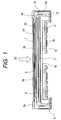
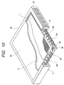
- FIG. 1 of the accompanying drawings schematically illustrates a known imaging apparatus of the above described type.
- FIG. 1 it comprises a fluorescent plate 1, photoelectric transfer elements 2a for converting visible light into electric signals, sensor substrates 2b, spacers 3a, TAB films 5a operating as flexible circuit substrates, a moisture-proof film 6, a base 7, an apparatus cabinet 8, a frame member 8a, a covering member (grid) 8b, a bottom member 8c, an adhesive layer 9, ICs 10a (for reading signals), radiator sheets 10c, circuit substrates 15, radiator fins 16 and spacers 17.
- Arrow 201 in FIG. 1 indicates the direction along which a load is normally applied to (or radioactive rays strike) the apparatus.
- the photoelectric transfer elements 2a typically comprises amorphous silicon film (hereinafter referred to as a-Si film) as photoelectric conversion layer because it can be formed with ease on a sensor substrate 2b that may be a glass substrate having a large surface area and it can be used not only for photoelectric transfer elements 2a but also as semiconductor material for preparing switch TFTs that operate as switching devices.
- a-Si film is popularly used as semiconductor material for preparing photoelectric transfer elements 2a because both photoelectric transfer elements 2a and their respective switch TFTs (not shown) can be formed on a glass substrate 2b in a same single process by using it as semiconductor material.
- a glass substrate is popularly used for each of the substrates (sensor substrates) 2b carrying photoelectric transfer elements 2a because they are required to be free from chemical reactions with the semiconductor devices of the apparatus, resist the high temperature of the semiconductor forming process and maintain dimensional stability.
- the fluorescent plate 1 is prepared by applying a fluorescent material of a metal compound to a resin plate.
- the gap separating the fluorescent plate 1 and the photoelectric transfer elements 2a has to be held to a sufficiently small value (typically less than tens of several ⁇ m) relative to the size of the pixels (more than a hundred ⁇ m) of the photoelectric transfer elements 2a and, in most cases, the fluorescent plate 1 and the substrates 2b are bonded together by means of an adhesive agent.
- both the fluorescent plate 1 and the photoelectric transfer elements 2a may be wrapped and hermetically sealed by a moisture-impermeable and X-ray transmissive film (e.g., evaporated Al film) 6.
- a moisture-impermeable and X-ray transmissive film e.g., evaporated Al film
- the drive circuit substrate 15 for driving the photoelectric transfer elements 2a and reading data therefrom is fitted to the rear surface of the sensor substrates 2b carrying the photoelectric transfer elements 2a thereon with spacers 17 interposed therebetween and subsequently semiconductor circuit devices (electronic components) 5c for driving the converters are mounted thereon.
- the substrates 2b are rigidly secured to the surface of the base 7 by means of an adhesive layer 9.
- the base 7 is fitted to the bottom plate 8c of the apparatus cabinet 8 with spacers 3a interposed therebetween, the bottom plate 8c being adapted to operate as holder for the above listed components.
- Such imaging apparatus are conventionally used for X-ray photography as stationary apparatus.
- imaging apparatus are conventionally used for X-ray photography as stationary apparatus.
- imaging apparatus there is an increasing demand for lightweight, compact and portable imaging apparatus adapted to rapid imaging operations for producing fine images.
- imaging apparatus having the above described configuration are required to safeguard the substrate 2b and other related components against impacts that can be applied thereto during transportation and the apparatus are also required to be safeguarded as a whole against deformation, e.g, that of the closure 8b of the apparatus cabinet 8, that can be caused by the external load 201 (mainly the weight of the person to be photographed) of the apparatus during X-ray photographing operations.
- heat-radiating members such as radiator fins 16 for releasing heat from the ICs (integrated circuit devices) 10a including signal reading ICs and driver ICs arranged on the flexible circuit substrate 5a
- a specifically prepared member has been proposed in order to shield the drive circuit and the ICs from X-rays and other radioactive rays because radioactive rays irradiated onto the apparatus can give rise to operation errors on the part of the semiconductor circuit devices (electronic components) 5c arranged on the drive circuit substrate 15 and the drive circuit including the drive ICs 10a arranged on the flexible circuit substrate 5a and even destruct the semiconductor circuit devices 5c.
- a lead plate may be used to completely cover the base in order to make the apparatus free from troubles attributable radioactive rays. Obviously, however, such an arrangement is against the attempt for producing a down-sized and lightweight imaging apparatus.
- the base 7 for holding the sensor substrates 2b carrying thereon photoelectric transfer elements 2a, the bottom plate 8c of the apparatus cabinet 8 rigidly securing the base 7, the frame member 8a of the apparatus cabinet 8 arranged around the above listed components, the heat-radiating members 16 of the drive ICs 10a and the lead plate (not shown) for shielding the apparatus against radioactive rays including X-rays are all heavy and bulky and hence operate against the attempt for realizing a lightweight imaging apparatus.
- the drive ICs, the signal reading ICs in particular have to be provided with respective heat-radiating members on a one-to-one basis in order to ensure stable temperature-related characteristics required for reading analog signals correctly.
- such an arrangement inevitably increase the number of components to operate against the attempt for realizing a down-sized imaging apparatus.
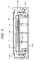
- FIG. 2 of the accompanying drawings is a schematic cross sectional view of another known imaging apparatus realized in the form of a cassette.
- the outer frame of the apparatus includes a grid 8b secured to an apparatus cabinet 8 by means of screws.
- a radiation-sensitive solid imaging section is arranged within range 5103 defined by dotted lines in the cassette in FIG. 2.
- FIGS. 3 and 4 respectively show a schematic cross sectional view and a schematic plan view of the radiation-sensitive solid imaging section. It includes sensor substrates 2b carrying on the upper surface thereof photoelectric transfer elements that operate as light receiving section of the apparatus and a pixel region 5205 where photoelectric transfer elements and TFT devices are arranged.
- the sensor substrates 2b and the base 7 supporting it are rigidly secured to each other by means of an adhesive agent 5207.
- the sensor substrates 2b are aligned with each other so as to two-dimensionally show a regular pitch of arrangement of pixels before they are rigidly secured onto the base 7 typically in order to produce a large substrate because the use of a plurality of small substrates is advantageous as they can be manufactured at high yield. In other words, it may be replaced by a single large substrate to eliminate the need of using a base if such large substrates can also be manufactured at high yield.
- the fluorescent plate 1 for converting radioactive rays into visible rays of light is typically prepared by applying a granular fluorescent material such as CaWO 4 or Gd 2 O 2 S:Tb 3+ onto a resin plate.
- reference numeral 5210 denotes drawer electrode sections for receiving input signals for driving the photoelectric transfer elements and the TFT devices from an input system and transmitting output signals obtained by reading X-ray information to an output system, said input system and said output system being external relative to the sensor substrates.
- the drawer electrode sections are connected respectively to printed circuit substrates 15 by way of flexible circuit substrates 5a, which flexible circuit substrates 5a carry ICs thereon, each being provided with an input signal or output signal processing circuit.
- a sealing member 5214 is arranged at the junction of each of the drawer electrode sections and the corresponding flexible circuit substrate and typically made of silicon resin, acrylic resin or epoxy resin.
- the moisture-proof film 6 that is impermeable to moisture and radiation transmittable is typically a metal film formed by evaporation of Al as described above.
- the metal film is arranged on the fluorescent plate with an adhesive layer 5216 interposed therebetween. This metal film is used to hermetically seal. the fluorescent plate, the photoelectric transfer elements and the TFT devices when the photoelectric transfer elements and the TFT devices are required to be protected against moisture and electromagnetic waves.
- a sealing material 5217 is applied onto the metal film to fill any possible gaps existing among the sensor substrates.
- the radiation-sensitive solid imaging section having a configuration as described above is then supported by support pillars 5104 within the cassette and rigidly secured to the support pillars 5104 and the closure 8b, which is a grid, by means of an adhesive agent or an agglutinative agent or by means of anchoring members 5105, each carrying an adhesive agent or a agglutinative agent on the top and under the bottom thereof.
- both the flexible circuit substrates 5a and the printed circuit substrates 15 are secured to the cabinet 8 by means of respective fitting plates 5106 and screws.
- the fitting plates 5106 are adapted to provide heat conduction paths leading to the cabinet 8 and the cabinet 8 is provided with plural vent holes 5107 to allow air to freely circulate within the cassette as heat releasing measures.
- radioactive rays coming from a radiation source and entering the cassette after passing through the object of inspection are converted into rays of visible light (having a wavelength sensed by the sensor) within the fluorescent plate.
- the obtained rays of visible light are then made to pass through the adhesive agent arranged directly below the fluorescent plate and enter the photoelectric transfer elements arranged on the sensor substrates.
- the light received by the photoelectric transfer elements is then photoelectrically converted and a two-dimensional image will be output therefrom.
- a transparent glass substrate 5501 may be arranged above the sensor substrates in a manner as shown in FIG. 5 of the accompanying drawings as preventive measures against mechanical impacts and electrolytic corrosion that the photoelectric transfer elements and the TFT devices can be subjected to, taking the high transmittability of light of the glass substrate.
- the solid imaging section is rigidly secured to the cabinet 8 as in the case of the radiation imaging section except the anchoring mode on the upper surface of the imaging section within the package.
- the upper surface of the imaging section and the cabinet 8 are secured to each other by means of keep plates 5403 anchored to the upper surface of the cabinet 8 with screws in an outer region of the transparent glass substrate 5501 located outside the pixel region of the apparatus.
- a large screen image sensor as described above, information on the image of the object is input to the photoelectric transfer elements directly or by way of an optical system comprising lenses and prisms to produce a two-dimensional image.
- an uneven temperature distribution of the photoelectric transfer element section can lead to fluctuations in the dark current, which by turn can remarkably differentiate the performance of the photoelectric transfer elements located close to the air vent holes 5107 and that of those located remote from them as the inside of the apparatus is cooled by air entering through the vent holes 5107. Then, the photoelectric transfer elements will not operate for imaging.
- Another object of the present invention is to provide an imaging apparatus that is conveniently portable and can suitably be used as a cassette.
- Still another object of the present invention is to provide an imaging apparatus that is free from the problem of heat emitted from the ICs of the apparatus used for driving devices and for various processing operations, particularly that may arise due to the positions of the photoelectric transfer elements within the apparatus so that it may operate stably and reliably for imaging.
- Still another object of the present invention is to provide an imaging apparatus that is down-sized and adapted to emit heat effectively and efficiently and comprise a reduced number of components so that the weight may be significantly reduced.
- a further object of the present invention is to provide an imaging apparatus that can input imaging information with an enhanced level of resolution, a high SN ratio and a high tone gradation.
- a still further object of the present invention is to provide an imaging apparatus comprising a substrate, photoelectric transfer elements arranged on the substrate, a semiconductor device located in association with the photoelectric transfer elements and a thermal device for discharging heat coming from the semiconductor device to the outside.
- FIGS. 1, 2 and 5 are schematic cross sectional views of an imaging apparatus.
- FIG. 3 is a schematic cross sectional view of the imaging section of an imaging apparatus.
- FIG. 4 is a schematic plan view of the imaging section of FIG. 3.
- FIGS. 6, 9, 11, 12, 17 and 18 are schematic cross sectional views of imaging apparatus comprising thermal devices.
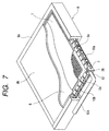
- FIGS. 7 and 10 are schematic perspective views of imaging apparatus.
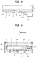
- FIG. 8 is a schematic cross sectional view of part of the apparatus of FIG. 7, showing part of its circuit section.
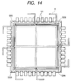
- FIGS. 13 and 14 are schematic plan views, illustrating how thermal devices can be fitted to the imaging section.
- FIG. 15 is a schematic cross sectional view of a Peltier device.
- FIG. 16 is a schematic cross sectional view, illustrating how thermal devices can be fitted in position.
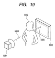
- FIG. 19 is a schematic perspective view of an imaging apparatus, illustrating how it is used in an instance of application.
- FIG. 6 is a schematic cross sectional view of an embodiment of imaging apparatus according to the present invention. It comprises a metal base plate carrying thereon a glass substrate with photoelectric transfer elements and containing therein heat pipes as heat conduction devices, or thermal devices.
- FIG. 7 is a schematic perspective view of the imaging apparatus of FIG. 6 and
- FIG. 8 is a schematic cross sectional view of part of the metal base 7, showing the arrangement of electronic parts thereof.
- FIGs. 6 and 7 there are shown a fluorescent plate 1, photoelectric transfer elements (sensors) 2a, sensor substrates 2b which are glass substrates in this embodiment, signal reading ICs 10a, driver ICs 10b, a base 7 having the role of a drive circuit substrate and that of the bottom section of an apparatus cabinet 8, being made of metal.
- it is made of A1 and adapted to conduct heat generated in the circuit devices of the drive circuit substrate through the base.
- TAB films 5a operating as flexible circuit substrates
- electronic devices e.g., semiconductor circuit devices
- 5c for driving the photoelectric transfer elements 2a mounted on the TAB films and reading information therefrom
- a frame 8a of the apparatus cabinet e.g., a closure 8b of the apparatus cabinet adapted to protect the photoelectric transfer elements 2a from above
- an adhesive layer 9a arranged between the sensor substrates 2b and the fluorescent plate 1 and heat pipes 12 buried partly in the base 7 and partly projecting out of the apparatus cabinet 8.
- Reference symbol 3a denotes spacers for anchoring the glass substrates 2b to the base 7
- reference symbol 12a denotes a heat radiating section of each of the heat pipes 12.
- FIG. 8 is a schematic cross sectional view of part of the metal base 7, showing an arrangement of electronic parts and so forth of the drive circuits disposed on the rear surface of the base 7.
- the drive circuit is formed by applying insulation films 14 on the principal metal material 13 and forming wires thereon and hence the base 7 operates as the drive circuit substrate.
- a Cu foil is bonded onto the insulation films 14 and subjected to a patterning operation to produce conductor sections 14a for the wires and electronic parts 5c are soldered to the respective conductor sections.
- solder resist may be applied except the terminal sections for connecting FPCs that operate as wiring members. If necessary, the terminal sections may be surface-treated (e.g., by solder plating) before forming drive circuits. Then, the electronic parts 5c are soldered to the conductor sections 14a to be used for soldering.
- the principal metal material 13 of the base 7 (also operating as the drive circuit substrate) is made of Pb or the surface (at the side of the glass substrates 2b) of the principal metal material 13 is coated with Pb, the electronic parts on the drive circuits can be shield from radiation. In other words, then the principal metal material can operate as radiation blocking member to consequently reduce the overall weight of the imaging apparatus.
- heat generated by the signal reading ICs and the driver ICs can be effectively released to the outside of the imaging apparatus.
- liquid contained in the heat pipes 12 within the base 7 is vaporized by heat radiated from the ICs so that heat may be transferred to the heat emitting sections 12a of the heat pipes 12.
- the photoelectric transfer elements can show a stable temperature level and operate stably in reading image information.
- FIG. 9 shows another embodiment using heat pipes.
- each of the heat pipes has an end buried in the base 7 and the other end adapted to operate as heat emitting section 12a that is provided with fins or some other heat emitting means.
- the cabinet 8 and the base 7 are thermally isolated from each other by means of thermal insulation members 901.
- the thermal energy discharged from the ICs 10a and other sources of heat is transmitted to the base 7 held in contact with the ICs 10a and then released to the outside through the heat emitting sections 12a of the heat pipes.
- the heat pipes 12 are separated from the cabinet and the base 7 is thermally isolated from the cabinet 8 by means of thermal insulation members 901, the temperature of the cabinet 8 does not rise or hardly rises if the imaging apparatus is operated continuously.
- the imaging apparatus does not provide any particularly hot areas on the surface in operation as the heat emitting sections are recessed. While an imaging apparatus adapted to photographing the human body by means of X-rays is often brought to contact with the body in operation, the safety of photographing of such an imaging apparatus will be ensured with the recessed arrangement of the heat emitting sections.
- FIG. 10 is a schematic perspective view of another embodiment of imaging apparatus according to the present invention.
- the heat pipes of the above embodiments are replaced with thermal devices, more specifically Peltier devices 11 that operate as thermal converters, that are arranged within the frame 8a of the apparatus cabinet 8 and held in contact with the ICs 10a.
- thermal devices more specifically Peltier devices 11 that operate as thermal converters
- heat generated by the signal reading ICs and the driver ICs can be effectively removed by means of the Peltier devices 11 to cool the former.
- any possible temperature rise of the ICs and other heat generating devices can be effectively suppressed without obstructing the attempt for reducing the overall weight of the imaging apparatus.
- Peltier devices 11 can be arranged individually near the respective devices that emit heat to further reduce the temperature difference among the devices if compared with the above instance of using heat pipes 12 so that both the size and the weight of the imaging apparatus can be further reduced with a satisfactory heat discharge level without raising the thermal capacity of the principal metal material of the base 7.
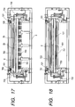
- FIGS. 11 and 12 are schematic cross sectional views of another embodiment of imaging apparatus according to the invention as viewed from two different sides.
- FIGS. 13 and 14 are schematic plan views of the imaging section of the embodiment as viewed from above and from below respectively.
- Reference numeral 101 in the drawings denotes Peltier devices.
- FIG. 15 is a schematic lateral view of a single stage Peltier device realized by alternately arranging p-type chips 1501 and n-type chips 1502 typically made of a thermoelectric semiconductor such as Bi 2 Te 3 on a plane and electrically connecting them in series by way of their ohmic electrodes 1503. The chips are then sandwiched at the opposite surfaces by and rigidly held to a pair of electrically insulated spacers typically made of aluminum/aluminum nitride.
- the spacers show a thermal conductivity as large as possible. Elements that have to be cooled are fitted to the upper spacer 1504, whereas those that emit heat are fitted to the lower spacer 1505.
- the Peltier device When the Peltier device is electrically energized, a large number of carriers are forced to move from left to right in FIG. 15 in both the p-type chips and the n-type chips to produce a flow of heat. As a result, the temperature of the top of the device falls, while that of the bottom of the device rises.
- a plurality of Peltier devices 101 are arranged on the rear side of the base, the cooling side of each of the Peltier devices 101 being connected to the rear surface of the base that rigidly holds the sensor substrates.
- the base indirectly cool the sensor substrates having a large surface area.
- Peltier devices are arranged in the pixel region 5205 in such a way that they cover a surface area greater than that of the pixel region.
- Peltier devices are preferably arranged only within the pixel region if they have a sufficiently large cooling capacity.
- the cooling capacity can be improved by reducing the thermal resistance of the thermal conduction path from the base to the sensor substrates in several different ways.
- Heat is transferred by way of the Peltier devices, the base, the adhesive agent between the base and the sensor substrates and the sensor substrates.
- the thermal resistance is a function of the thermal conductivity and the profile (the area of the cross section, the length along which heat is conducted) of each of the components.
- the thermal resistance can be reduced when the components are made of materials having a high thermal conductivity and have a reduced length and a large cross sectional area, provided that they are connected well relative to each other in very minute surface area.
- the most preferable materials to be used for forming the base and the sensor substrates include metals and alloys such as iron, stainless steel, aluminum, copper, brass, lead and magnesium alloy, ceramic materials such as silicon carbide, beryllia porcelain, aluminum nitride and boron nitride, organic resin such as graphite sheet and metal oxide such as aluminum oxide and ITO, that show a thermal conductivity of not lower than 10W/m ⁇ °C at room temperature. Glass substrates are preferably used for the sensor substrates in view of forming a semiconductor layer thereon.
- the base carries thereon a plurality of sensor substrates that are rigidly secured to the base and aligned with each other so as to two-dimensionally show a regular pitch of arrangement of pixels.
- both the sensor substrates and the base are preferably made of a same material so that they show a same thermal expansion coefficient.
- Glass shows a poor thermal conductivity of about 3W/m ⁇ °C and, therefore, if glass is used for the sensor substrates, they are preferably coated with metal or metal oxide such as aluminum, chromium or ITO by means of evaporation or plating.
- the base is subjected to the above process over the entire surface, whereas the above process is conducted at least the pixel region on the rear surface of each of the sensor substrates. As a result, the surface thermal resistance of the components is reduced to provide thermal conduction paths on the surfaces of the components.
- a thermally conductive resin material such as silicon grease or silicon rubber may advantageously be used to connect the above components.
- a resin material that is an adhesive or agglutinative agent containing solder or electroconductive paste or a powdery material having a thermal conductivity of not lower than 10W/m ⁇ °C as described above may preferably be used.
- Peltier devices may be formed directly on the base in order to establish an improved connection between the Peltier devices and the base.
- the above description applies to radiation-sensitive imaging apparatus comprising a plurality of small sensor substrates to produce a large surface area.
- a single sensor substrate having a large surface area is produced, then only Peltier devices will have to be connected to the rear surface of the sensor substrate without using a base.
- at least the pixel region of the rear surface of each of the sensor substrates is coated with a material having a thermal conductivity of not lower than 10W/m ⁇ °C.
- the Peltier devices may be connected to the related sensor substrates either directly or by means of a thermally conductive resin material.
- FIG. 14 is a plan view of the radiation-sensitive imaging section of an imaging apparatus according to the invention, showing how Peltier devices are arranged. Since Peltier devices are arranged outside and very close to the pixel region to surround the latter in order not to interfere with the passage of X-ray information entering the pixel region but to minimize the thermal resistance and produce an efficient cooling effect. Note that the metal films having the edges covered by the sealing material are located between the sealing material and the pixel region. The Peltier devices and the related metal films are connected by means of a thermally conductive resin material or as the metal films are directly formed on the respective Peltier devices. As a result, the upper surfaces of the sensor substrates will be cooled evenly by way of the metal films, using the metal films as heat diffusion plates.
- cooling means may alternatively be used in place of the Peltier devices arranged on the rear surfaces of the sensor substrates so long as such means can evenly cool the upper surfaces of the sensor substrate to produce a uniform temperature distribution pattern.
- reference numeral 12 denotes heat pipes.
- a heat pipe When compared with metal that is a conductor of heat, a heat pipe operates far better for transmitting heat, showing a much higher thermal conductivity than metal.
- the heat pipe are fitted at an end thereof to the heat emitting sides of the respective Peltier devices and at the other end to the cabinet 8 that also shows a high thermal conductivity.
- the cabinet 8 is typically made of a material that has an excellent mechanical strength and a thermal conductivity not lower than 10W/m ⁇ °C such as magnesium alloy or aluminum.
- the heat pipes are preferably deformable so that they may be arranged appropriately in the narrow inside of the cabinet 8 and provide desired paths for heat.
- each heat pipe 12 may be arranged between a metal fitting 601 and the cabinet 8 and pinched at the opposite sides thereof by a thermally conductive resin 602 such as silicon rubber and rubber 603 as shown in FIG. 16 before screw 604 is tightened so that the cabinet 8 and the heat pipe 12 may be securely held in position under the pressure applied by the fitting plate.
- the heat generated in the Peltier device as a result may be transmitted to the cabinet 8 by way of the heat pipe.
- the temperature of the sensor substrates that require cooling may be maintained by keeping them away from direct contact with any components whose temperature is higher than that of the sensor substrates and/or by arranging a closed space around them without causing any significant convention to take place in it.
- FIGS. 11 and 12 show such an arrangement of keeping the temperature of the sensor substrates within a desired range.
- the outer support pillars 104 connect the bottom surface and the top surface of the cabinet 8 and surround the four peripheral edges of the assembly of the sensor substrates 2b including the base 7.
- the support pillars 104 are provided with holes for allowing heat pipes 12 and the flexible circuit substrates to pass therethrough and the gap of each of the holes separating the hole and the heat pipe 12 or the flexible circuit substrate, whichever appropriate, is filled with resin.
- the space surrounding the sensor substrates including the base 7 is completely closed by and hermetically sealed by the support pillars 104, the grid and the cabinet 8.
- the imaging section is rigidly secured to the grid 8b and the support pillars 104 by means of an adhesive agent or an agglutinative agent or by way of anchoring members 106, each carrying an adhesive or an agglutinative agent on the top and under the bottom thereof.
- the anchoring members 106 are made of a material having a low thermal conductivity that may be a polymer material such as polyethylene resin, epoxy rein or polyurethane resin.
- FIGS. 17 and 18 are schematic cross sectional views of a still another embodiment of imaging apparatus according to the invention as viewed along two different directions.
- the components same as and similar to their counterparts of the other embodiments will be denoted respectively by the same reference symbols and will not be described further.
- a heat sink 701 is arranged on each of the Peltier device 101 in the above described manner. Heat is forcibly released from the heat sink 701 by means of an exhaust fan 702 arranged in a lower portion of the cabinet at the rear surface side of the base.
- the support pillars and the cabinet are provided with holes for promoting ventilation.
- the heat sinks 701 arranged on the metal film operating as moisture-proof film 6 are exposed to the outside of the cabinet at the front end thereof through the respective holes bored through the grid so that they may be cooled by ambient air. Thus, heat generated by the Peltier devices is released into ambient air by way of the heat sinks.
- the related regions should preferably be well ventilated.
- the sensor substrates 2b including the base 7 are pinched by a pair of insulation plates 703 at the top and at the bottom.
- the insulation plates 703 have a profile same as the frame surrounded by the support pillars 704 at the four sides and a thickness smaller than the sum of the height of the Peltier devices 101 and that of the heat sinks 701.
- the insulation plates 703 are cut out in areas corresponding to the Peltier devices, the support pillars 704 and the anchoring members 106 of the sensor substrates 2b.
- the insulation plates are made of a polymer material such as polyethylene resin, epoxy resin or polyurethane resin.
- the sensor substrates are hermetically sealed by the upper and lower insulation plates and the support pillars and cooled to a desired temperature range.
- an imaging apparatus that is compact and lightweight and can be handled with ease.
- an imaging apparatus that is conveniently portable and can suitably be used as a cassette.
- an imaging apparatus that can effectively cool its semiconductor devices including drive ICs such as photoelectric transfer elements and electric signal processing ICs to stabilize the performance of the semiconductor devices in order to stably output signals with a high SN ratio.
- an imaging apparatus that can reliably and accurately provide image information because the light receiving section thereof comprising photoelectric transfer elements is so adapted as not to produce or to hardly produce an unnecessary thermal distribution pattern due to heat emitted from the semiconductor devices.
- the imaging apparatus can provide imaging information with a high tone gradation and an enhanced level of resolution.
- an imaging apparatus since the base for supporting the glass substrates that carry thereon photoelectric transfer elements also operates as support for the electronic parts used for them and is typically made of aluminum or lead so that both the overall weight and the number of components of the apparatus can be reduced without sacrificing its strength. Therefore, according to the present invention, there is provided a lightweight and compact imaging apparatus that performs excellently for using a radiation source.
- an imaging apparatus may comprise thermal converters such as heat pipes or Peltier devices arranged within the metal material of its base or the frame of the apparatus cabinet containing the base so that heat emitted from the drive ICs, the signal reading ICs and the peripheral circuits of the apparatus can effectively be released to the outside.
- thermal converters such as heat pipes or Peltier devices arranged within the metal material of its base or the frame of the apparatus cabinet containing the base so that heat emitted from the drive ICs, the signal reading ICs and the peripheral circuits of the apparatus can effectively be released to the outside.
- the principal metal material of the base is made of lead, it can also operate as shield for blocking radiation so that the apparatus can efficiently emit heat without making itself bulky by using additional shield member.
- an imaging apparatus may comprise thermal converters such as heat pipes or Peltier devices arranged at least in the pixel region on the rear surface of the sensor substrates or of the base rigidly securing the sensor substrates so that a large area can be cooled to show a uniform temperature distribution pattern and the thermal noise and the dark current of the photoelectric transfer elements can be reduced to improve the resolution and realize a high SN ratio.
- thermal converters such as heat pipes or Peltier devices arranged at least in the pixel region on the rear surface of the sensor substrates or of the base rigidly securing the sensor substrates so that a large area can be cooled to show a uniform temperature distribution pattern and the thermal noise and the dark current of the photoelectric transfer elements can be reduced to improve the resolution and realize a high SN ratio.
- an imaging apparatus is made to comprise a metal film arranged above the sensor substrates as in the case of a radiation-sensitive imaging apparatus
- Peltier devices may be arranged on the metal film in areas not corresponding to the pixel region (non-pixel region) to produce a cooling effect more effective than the one that can be obtained on the upper surface of the sensor substrates and improve the resolution.
- the cooling efficiency of any desired portion thereof can be improved to reduce both the power consumption rate of the devices and the operating cost of the apparatus by making such an arrangement that heat generated by the Peltier devices is discharged by way of heat pipes or heat sinks, that the sensor substrates, the base and the adhesive agent are made of respective materials that are thermally highly conductive, that the contact resistance of the components of the apparatus is reduced by using thermally conductive resin and that the sensor substrates are hermetically sealed by means of the cabinet, the support pillars, the grid and the thermal insulators of the apparatus.
- a cooling system using a cooling medium such as liquefied nitrogen or a gaseous cooling medium such as carbon dioxide so that the imaging apparatus can be made very compact and provide an improved maintainability.
- an imaging apparatus since the heat emitting section can be arranged without projecting from the cabinet, the cabinet and the outer cover that are the outermost components to be put to contact with the object of imaging are kept free from high temperature while heat generated in the inside can be safely released to the outside. Therefore, such an imaging apparatus can be used for a radiation-sensing cassette that is safe and easy to handle.
- an imaging apparatus can meet the demand of the market of medical equipment and imaging equipment for apparatus capable of producing high quality images.
- the present invention is suitably applicable to radiation-photographing imaging apparatus.
- an imaging apparatus according to the present invention can suitably be used for X-ray image diagnosis of the chest, the abdomen or the breast of the patient. More specifically, a large assembly of sensor substrates having a large light receiving area of 100x100mm to 500x500mm will be used for such an apparatus so that it can provide high sensitivity/high resolution image information on any fine shade in a minute area of the examined local portion of the body can be detected.
- an X-ray image can be obtained by irradiating the subject 5002 with X-rays 5004 emitted from X-ray source 5001 and converting the transmitted X-rays 5005 into electric signals by means the photoelectric transfer elements of the light receiving section of the imaging apparatus 5003.
Landscapes
- Physics & Mathematics (AREA)
- Health & Medical Sciences (AREA)
- Life Sciences & Earth Sciences (AREA)
- General Physics & Mathematics (AREA)
- High Energy & Nuclear Physics (AREA)
- Molecular Biology (AREA)
- Spectroscopy & Molecular Physics (AREA)
- Solid State Image Pick-Up Elements (AREA)
- Transforming Light Signals Into Electric Signals (AREA)
- Measurement Of Radiation (AREA)
- Cooling Or The Like Of Semiconductors Or Solid State Devices (AREA)
Applications Claiming Priority (4)
| Application Number | Priority Date | Filing Date | Title |
|---|---|---|---|
| JP06530598 | 1998-03-16 | ||
| JP6530598 | 1998-03-16 | ||
| JP11061576A JPH11345956A (ja) | 1998-03-16 | 1999-03-09 | 撮像装置 |
| JP06157699 | 1999-03-09 |
Publications (2)
| Publication Number | Publication Date |
|---|---|
| EP0943931A2 true EP0943931A2 (de) | 1999-09-22 |
| EP0943931A3 EP0943931A3 (de) | 2000-08-23 |
Family
ID=26402624
Family Applications (1)
| Application Number | Title | Priority Date | Filing Date |
|---|---|---|---|
| EP99301982A Withdrawn EP0943931A3 (de) | 1998-03-16 | 1999-03-15 | Bilderzeugungsapparat |
Country Status (3)
| Country | Link |
|---|---|
| US (1) | US6323891B1 (de) |
| EP (1) | EP0943931A3 (de) |
| JP (1) | JPH11345956A (de) |
Cited By (12)
| Publication number | Priority date | Publication date | Assignee | Title |
|---|---|---|---|---|
| WO2001071383A1 (fr) * | 2000-03-21 | 2001-09-27 | Commissariat A L'energie Atomique | DETECTEUR DE RAYONNEMENT A JONCTION SEMI-CONDUCTRICE POUR LA MESURE DE FORTS DEBITS DE DOSE DE RAYONNEMENT X OU $g(g) |
| EP1262821A1 (de) * | 2001-05-30 | 2002-12-04 | Canon Kabushiki Kaisha | Röntgenapparat |
| WO2003021682A1 (en) * | 2001-08-30 | 2003-03-13 | Acrorad Co., Ltd. | Radiation image detector |
| EP1227702A3 (de) * | 2001-01-30 | 2003-05-02 | Samsung Electronics Co., Ltd. | Optisches Bauelement-Modul versehen mit einem Wärmeträger durch Phasenübergang |
| WO2004036249A1 (en) * | 2002-10-18 | 2004-04-29 | Koninklijke Philips Electronics N.V. | Continuous moisture getter for a solid state detector |
| EP2362240A1 (de) * | 2010-02-26 | 2011-08-31 | Fujifilm Corporation | Tragbares Röntgenbildgebungsgerät |
| US8222612B2 (en) * | 2007-09-28 | 2012-07-17 | Fujifilm Corporation | Radiation image capturing apparatus |
| EP2693269A1 (de) * | 2012-08-01 | 2014-02-05 | Fujifilm Corporation | Röntgenbildgebungsvorrichtung |
| WO2014025543A1 (en) * | 2012-08-08 | 2014-02-13 | General Electric Company | Digital x-ray detector assembly with elastomeric backscatter shield |
| EP2719333A3 (de) * | 2012-10-12 | 2014-05-21 | GE Medical Systems Global Technology Company LLC | Kühlerloses Kühlsystem und Verfahren für interventionellen Detektor |
| CN105474045A (zh) * | 2013-08-19 | 2016-04-06 | 株式会社东芝 | 辐射检测器 |
| DE102015115121B4 (de) * | 2014-09-10 | 2025-10-02 | Canon Kabushiki Kaisha | Strahlungsbilderzeugungsgerät und Strahlungsbilderzeugungssystem |
Families Citing this family (57)
| Publication number | Priority date | Publication date | Assignee | Title |
|---|---|---|---|---|
| JP4442833B2 (ja) * | 1998-08-04 | 2010-03-31 | キヤノン株式会社 | 光電変換装置 |
| US6617671B1 (en) * | 1999-06-10 | 2003-09-09 | Micron Technology, Inc. | High density stackable and flexible substrate-based semiconductor device modules |
| DE10004891C2 (de) * | 2000-02-04 | 2002-10-31 | Astrium Gmbh | Fokalfläche und Detektor für optoelektronische Bildaufnahmesysteme, Herstellungsverfahren und optoelektronisches Bildaufnahmesystem |
| JP2001318155A (ja) * | 2000-02-28 | 2001-11-16 | Toshiba Corp | 放射線検出器、およびx線ct装置 |
| JP2011248382A (ja) * | 2000-06-27 | 2011-12-08 | Canon Inc | X線検出器 |
| JP4447752B2 (ja) * | 2000-08-03 | 2010-04-07 | 浜松ホトニクス株式会社 | 放射線検出器 |
| JP4283427B2 (ja) | 2000-08-03 | 2009-06-24 | 浜松ホトニクス株式会社 | 放射線検出器およびシンチレータパネル |
| JP4759131B2 (ja) * | 2000-11-21 | 2011-08-31 | キヤノン株式会社 | X線画像撮影装置 |
| DE10100679A1 (de) * | 2001-01-09 | 2002-07-11 | Abb Research Ltd | Träger für Bauelemente der Mikrosystemtechnik |
| JP2002214352A (ja) * | 2001-01-19 | 2002-07-31 | Canon Inc | 放射線画像撮影装置 |
| JP2003060948A (ja) * | 2001-06-05 | 2003-02-28 | Seiko Precision Inc | 固体撮像装置 |
| JP2003194951A (ja) * | 2001-12-28 | 2003-07-09 | Canon Inc | X線撮影装置 |
| JP2004219318A (ja) * | 2003-01-16 | 2004-08-05 | Hamamatsu Photonics Kk | 放射線検出器 |
| JP4253557B2 (ja) * | 2003-10-06 | 2009-04-15 | オリンパス株式会社 | 撮像装置 |
| US7313921B2 (en) * | 2003-10-28 | 2008-01-01 | General Electric Company | Apparatus and method for thermo-electric cooling |
| US7317190B2 (en) * | 2004-09-24 | 2008-01-08 | General Electric Company | Radiation absorbing x-ray detector panel support |
| US7866163B2 (en) * | 2004-10-04 | 2011-01-11 | General Electric Company | Radiographic detector docking station with dynamic environmental control |
| US7046764B1 (en) | 2004-10-04 | 2006-05-16 | General Electric Company | X-ray detector having an accelerometer |
| US7189972B2 (en) * | 2004-10-04 | 2007-03-13 | General Electric Company | X-ray detector with impact absorbing cover |
| US7342998B2 (en) * | 2004-11-18 | 2008-03-11 | General Electric Company | X-ray detector quick-connect connection system |
| US7381964B1 (en) | 2004-11-24 | 2008-06-03 | General Electric Company | Method and system of x-ray data calibration |
| US7581885B2 (en) | 2004-11-24 | 2009-09-01 | General Electric Company | Method and system of aligning x-ray detector for data acquisition |
| JP2006242702A (ja) * | 2005-03-02 | 2006-09-14 | Fuji Photo Film Co Ltd | 放射線検出用カセッテ |
| KR100741089B1 (ko) * | 2005-12-05 | 2007-07-20 | 삼성에스디아이 주식회사 | 방열구조 및 이를 구비한 플라즈마 디스플레이 장치 |
| DE102006010004B4 (de) * | 2006-03-03 | 2016-10-13 | Siemens Healthcare Gmbh | Röntgendetektor |
| JP4753763B2 (ja) * | 2006-03-28 | 2011-08-24 | 富士フイルム株式会社 | 放射線画像情報撮影装置 |
| US7834325B2 (en) * | 2006-03-24 | 2010-11-16 | Fujifilm Corporation | Radiation image information capturing apparatus and method of detecting temperature of amplifier thereof |
| JP4807121B2 (ja) * | 2006-03-24 | 2011-11-02 | 株式会社島津製作所 | 放射線検出装置 |
| US7926173B2 (en) * | 2007-07-05 | 2011-04-19 | Occam Portfolio Llc | Method of making a circuit assembly |
| US7495227B2 (en) * | 2007-07-10 | 2009-02-24 | General Electric Company | Digital x-ray detectors |
| JP4911312B2 (ja) * | 2007-07-13 | 2012-04-04 | 株式会社島津製作所 | 撮像装置 |
| JP2009066257A (ja) | 2007-09-14 | 2009-04-02 | Fujifilm Corp | 放射線画像撮影装置 |
| US20090078879A1 (en) * | 2007-09-25 | 2009-03-26 | Fujifilm Corporation | Image detecting device and image capturing system |
| US8294113B2 (en) | 2007-09-28 | 2012-10-23 | Fujifilm Corporation | Image detecting device and image capturing system |
| JP2009098136A (ja) * | 2007-09-28 | 2009-05-07 | Fujifilm Corp | 画像検出器及び画像撮影システム |
| JP4543339B2 (ja) * | 2007-12-14 | 2010-09-15 | ソニー株式会社 | 撮像装置 |
| JP5197265B2 (ja) * | 2008-09-22 | 2013-05-15 | 富士フイルム株式会社 | 放射線撮影装置 |
| JP2010262134A (ja) * | 2009-05-07 | 2010-11-18 | Fujifilm Corp | 放射線検出装置及び放射線画像撮影システム |
| JP5451265B2 (ja) * | 2009-08-31 | 2014-03-26 | キヤノン株式会社 | 放射線撮影装置 |
| JP2011059058A (ja) * | 2009-09-14 | 2011-03-24 | Fujifilm Corp | 放射線画像撮影装置 |
| US8711447B2 (en) * | 2010-05-19 | 2014-04-29 | Kabushiki Kaisha Toshiba | Image scanning apparatus and image forming apparatus |
| JP2012042302A (ja) * | 2010-08-18 | 2012-03-01 | Fujifilm Corp | 放射線撮影用カセッテ |
| JP5646289B2 (ja) * | 2010-11-09 | 2014-12-24 | 株式会社東芝 | 放射線検出装置 |
| US8829454B2 (en) * | 2012-02-27 | 2014-09-09 | Analog Devices, Inc. | Compact sensor module |
| JP5650168B2 (ja) * | 2012-07-27 | 2015-01-07 | 富士フイルム株式会社 | 放射線画像撮影装置 |
| US9116022B2 (en) | 2012-12-07 | 2015-08-25 | Analog Devices, Inc. | Compact sensor module |
| US9397134B1 (en) | 2013-02-07 | 2016-07-19 | Google Inc. | Methods and devices configured to provide selective heat transfer of an integrated circuit |
| JP2015068653A (ja) * | 2013-09-26 | 2015-04-13 | キヤノン株式会社 | 放射線撮像装置、その製造方法及び放射線検査装置 |
| JP6554840B2 (ja) * | 2015-03-16 | 2019-08-07 | 日本電気株式会社 | 固体撮像装置および固体撮像装置放熱方法 |
| KR102617349B1 (ko) * | 2016-12-02 | 2023-12-26 | 삼성전자주식회사 | 인쇄회로기판, 및 이를 가지는 솔리드 스테이트 드라이브 장치 |
| US12002838B2 (en) | 2018-12-06 | 2024-06-04 | Analog Devices, Inc. | Shielded integrated device packages |
| EP3891793A4 (de) | 2018-12-06 | 2022-10-05 | Analog Devices, Inc. | Integrierte vorrichtungspackungen mit passiven vorrichtungsanordnungen |
| WO2020202789A1 (ja) * | 2019-03-29 | 2020-10-08 | ソニーセミコンダクタソリューションズ株式会社 | センサ装置 |
| US11664340B2 (en) | 2020-07-13 | 2023-05-30 | Analog Devices, Inc. | Negative fillet for mounting an integrated device die to a carrier |
| US20240429253A1 (en) * | 2021-10-27 | 2024-12-26 | Sony Semiconductor Solutions Corporation | Semiconductor apparatus and electronic device |
| JP2023108947A (ja) * | 2022-01-26 | 2023-08-07 | キヤノン株式会社 | 放射線撮影装置および放射線撮影システム |
| JP2024158351A (ja) * | 2023-04-27 | 2024-11-08 | 浜松ホトニクス株式会社 | 放射線撮像装置 |
Family Cites Families (11)
| Publication number | Priority date | Publication date | Assignee | Title |
|---|---|---|---|---|
| US4230945A (en) | 1978-04-24 | 1980-10-28 | Meir Vladimir A | Device for detecting ionizing radiation |
| JPS593069B2 (ja) * | 1982-06-07 | 1984-01-21 | 日本電気株式会社 | 固体撮像装置 |
| JPS63284485A (ja) | 1987-05-15 | 1988-11-21 | Shimadzu Corp | 放射線像受像装置 |
| JPH01114780A (ja) * | 1987-10-28 | 1989-05-08 | Kanegafuchi Chem Ind Co Ltd | X線検出装置 |
| FR2625332A1 (fr) | 1987-10-27 | 1989-06-30 | Walter Jean Jacques | Capteur pour gamma camera, scanner et radiologie numerique |
| JP3284585B2 (ja) * | 1992-04-10 | 2002-05-20 | ソニー株式会社 | 電子機器の冷却装置 |
| JPH05333157A (ja) * | 1992-05-28 | 1993-12-17 | Shimadzu Corp | 放射線検出器 |
| US5596200A (en) | 1992-10-14 | 1997-01-21 | Primex | Low dose mammography system |
| JP3310404B2 (ja) * | 1993-07-23 | 2002-08-05 | 浜松ホトニクス株式会社 | 冷却型固体撮像装置 |
| US5596228A (en) * | 1994-03-10 | 1997-01-21 | Oec Medical Systems, Inc. | Apparatus for cooling charge coupled device imaging systems |
| JP3957803B2 (ja) * | 1996-02-22 | 2007-08-15 | キヤノン株式会社 | 光電変換装置 |
-
1999
- 1999-03-09 JP JP11061576A patent/JPH11345956A/ja not_active Withdrawn
- 1999-03-12 US US09/266,828 patent/US6323891B1/en not_active Expired - Lifetime
- 1999-03-15 EP EP99301982A patent/EP0943931A3/de not_active Withdrawn
Cited By (20)
| Publication number | Priority date | Publication date | Assignee | Title |
|---|---|---|---|---|
| FR2806807A1 (fr) * | 2000-03-21 | 2001-09-28 | Commissariat Energie Atomique | Detecteur de rayonnement a jonction semi-conductrice pour la mesure de forts debits de dose de rayonnement x ou gamma |
| WO2001071383A1 (fr) * | 2000-03-21 | 2001-09-27 | Commissariat A L'energie Atomique | DETECTEUR DE RAYONNEMENT A JONCTION SEMI-CONDUCTRICE POUR LA MESURE DE FORTS DEBITS DE DOSE DE RAYONNEMENT X OU $g(g) |
| EP1227702A3 (de) * | 2001-01-30 | 2003-05-02 | Samsung Electronics Co., Ltd. | Optisches Bauelement-Modul versehen mit einem Wärmeträger durch Phasenübergang |
| EP1262821A1 (de) * | 2001-05-30 | 2002-12-04 | Canon Kabushiki Kaisha | Röntgenapparat |
| US7104686B2 (en) | 2001-05-30 | 2006-09-12 | Canon Kabushiki Kaisha | Radiographic apparatus |
| US7537385B2 (en) | 2001-05-30 | 2009-05-26 | Canon Kabushiki Kaisha | Radiographic apparatus |
| US7575374B2 (en) | 2001-05-30 | 2009-08-18 | Canon Kabushiki Kaisha | Radiographic apparatus |
| WO2003021682A1 (en) * | 2001-08-30 | 2003-03-13 | Acrorad Co., Ltd. | Radiation image detector |
| WO2004036249A1 (en) * | 2002-10-18 | 2004-04-29 | Koninklijke Philips Electronics N.V. | Continuous moisture getter for a solid state detector |
| US7030387B2 (en) | 2002-10-18 | 2006-04-18 | Koninklijke Philips Electronics N.V. | Continuous moisture getter for solid state detector |
| US8222612B2 (en) * | 2007-09-28 | 2012-07-17 | Fujifilm Corporation | Radiation image capturing apparatus |
| EP2362240A1 (de) * | 2010-02-26 | 2011-08-31 | Fujifilm Corporation | Tragbares Röntgenbildgebungsgerät |
| EP2693269A1 (de) * | 2012-08-01 | 2014-02-05 | Fujifilm Corporation | Röntgenbildgebungsvorrichtung |
| WO2014025543A1 (en) * | 2012-08-08 | 2014-02-13 | General Electric Company | Digital x-ray detector assembly with elastomeric backscatter shield |
| US8680475B2 (en) | 2012-08-08 | 2014-03-25 | General Electric Company | Digital X-ray detector assembly with elastomeric backscatter shield |
| EP2719333A3 (de) * | 2012-10-12 | 2014-05-21 | GE Medical Systems Global Technology Company LLC | Kühlerloses Kühlsystem und Verfahren für interventionellen Detektor |
| US9301425B2 (en) | 2012-10-12 | 2016-03-29 | Ge Medical Systems Global Technology Company, Llc | Chiller-less cooling system and method for interventional detector |
| CN105474045A (zh) * | 2013-08-19 | 2016-04-06 | 株式会社东芝 | 辐射检测器 |
| EP3037844A4 (de) * | 2013-08-19 | 2017-04-12 | Toshiba Electron Tubes & Devices Co., Ltd. | Strahlungsdetektor |
| DE102015115121B4 (de) * | 2014-09-10 | 2025-10-02 | Canon Kabushiki Kaisha | Strahlungsbilderzeugungsgerät und Strahlungsbilderzeugungssystem |
Also Published As
| Publication number | Publication date |
|---|---|
| US6323891B1 (en) | 2001-11-27 |
| EP0943931A3 (de) | 2000-08-23 |
| JPH11345956A (ja) | 1999-12-14 |
Similar Documents
| Publication | Publication Date | Title |
|---|---|---|
| US6323891B1 (en) | Imaging apparatus with thermal discharger for transferring heat to cool photoelectric transfer elements | |
| US6667480B2 (en) | Radiation image pickup device and system | |
| US7629587B2 (en) | Radiation imaging apparatus | |
| US7791035B2 (en) | Electronic cassette type of radiation detection apparatus | |
| EP0791964B1 (de) | Photoelektrische Umwandlungsvorrichtung | |
| JP2001099942A (ja) | X線平面検出装置 | |
| US6495836B1 (en) | Two-dimensional image pickup apparatus | |
| US20130301808A1 (en) | Electronic cassette for radiographic imaging | |
| JP2003194951A (ja) | X線撮影装置 | |
| JP2000258541A (ja) | 放射線検出装置 | |
| CN114829983B (zh) | 射线照相检测器读取 | |
| JPH10177224A (ja) | X線撮影装置 | |
| US10341581B2 (en) | Radiographic detector with heat sink | |
| JP2012088152A (ja) | 放射線検出装置 | |
| JP2002131437A (ja) | X線画像撮影装置 | |
| US20190353810A1 (en) | Radiographic detector | |
| US20200121273A1 (en) | Radiographic detector | |
| JP4087028B2 (ja) | 外部回路実装方法および熱圧着装置 | |
| JP2002006049A (ja) | X線デジタル撮影装置 | |
| JP5499851B2 (ja) | 二次元画像検出器 | |
| JP2000116633A (ja) | 放射線撮影装置 | |
| JP2012122841A (ja) | 電子カセッテ | |
| JPH10146332A (ja) | X線ct装置 | |
| JP2009018109A (ja) | X線診断装置 | |
| JP2023117516A (ja) | 放射線の検出器 |
Legal Events
| Date | Code | Title | Description |
|---|---|---|---|
| PUAI | Public reference made under article 153(3) epc to a published international application that has entered the european phase |
Free format text: ORIGINAL CODE: 0009012 |
|
| AK | Designated contracting states |
Kind code of ref document: A2 Designated state(s): DE FR GB IT NL |
|
| AX | Request for extension of the european patent |
Free format text: AL;LT;LV;MK;RO;SI |
|
| PUAL | Search report despatched |
Free format text: ORIGINAL CODE: 0009013 |
|
| AK | Designated contracting states |
Kind code of ref document: A3 Designated state(s): AT BE CH CY DE DK ES FI FR GB GR IE IT LI LU MC NL PT SE |
|
| AX | Request for extension of the european patent |
Free format text: AL;LT;LV;MK;RO;SI |
|
| RIC1 | Information provided on ipc code assigned before grant |
Free format text: 7G 01T 1/29 A, 7G 01T 1/00 B, 7G 01T 1/24 B |
|
| 17P | Request for examination filed |
Effective date: 20010123 |
|
| AKX | Designation fees paid |
Free format text: DE FR GB IT NL |
|
| 17Q | First examination report despatched |
Effective date: 20040806 |
|
| STAA | Information on the status of an ep patent application or granted ep patent |
Free format text: STATUS: THE APPLICATION HAS BEEN WITHDRAWN |
|
| 18W | Application withdrawn |
Effective date: 20041209 |