EP0880176B1 - Dispositif semiconducteur avec pastille montée sur une plaque de radiation - Google Patents
Dispositif semiconducteur avec pastille montée sur une plaque de radiation Download PDFInfo
- Publication number
- EP0880176B1 EP0880176B1 EP98108897A EP98108897A EP0880176B1 EP 0880176 B1 EP0880176 B1 EP 0880176B1 EP 98108897 A EP98108897 A EP 98108897A EP 98108897 A EP98108897 A EP 98108897A EP 0880176 B1 EP0880176 B1 EP 0880176B1
- Authority
- EP
- European Patent Office
- Prior art keywords
- radiating plate
- pellet
- semiconductor device
- central portion
- lead terminals
- Prior art date
- Legal status (The legal status is an assumption and is not a legal conclusion. Google has not performed a legal analysis and makes no representation as to the accuracy of the status listed.)
- Expired - Lifetime
Links
Images


Classifications
-
- H—ELECTRICITY
- H01—ELECTRIC ELEMENTS
- H01L—SEMICONDUCTOR DEVICES NOT COVERED BY CLASS H10
- H01L23/00—Details of semiconductor or other solid state devices
- H01L23/28—Encapsulations, e.g. encapsulating layers, coatings, e.g. for protection
-
- H—ELECTRICITY
- H01—ELECTRIC ELEMENTS
- H01L—SEMICONDUCTOR DEVICES NOT COVERED BY CLASS H10
- H01L23/00—Details of semiconductor or other solid state devices
- H01L23/48—Arrangements for conducting electric current to or from the solid state body in operation, e.g. leads, terminal arrangements ; Selection of materials therefor
- H01L23/488—Arrangements for conducting electric current to or from the solid state body in operation, e.g. leads, terminal arrangements ; Selection of materials therefor consisting of soldered or bonded constructions
- H01L23/495—Lead-frames or other flat leads
- H01L23/49568—Lead-frames or other flat leads specifically adapted to facilitate heat dissipation
-
- H—ELECTRICITY
- H01—ELECTRIC ELEMENTS
- H01L—SEMICONDUCTOR DEVICES NOT COVERED BY CLASS H10
- H01L2224/00—Indexing scheme for arrangements for connecting or disconnecting semiconductor or solid-state bodies and methods related thereto as covered by H01L24/00
- H01L2224/01—Means for bonding being attached to, or being formed on, the surface to be connected, e.g. chip-to-package, die-attach, "first-level" interconnects; Manufacturing methods related thereto
- H01L2224/42—Wire connectors; Manufacturing methods related thereto
- H01L2224/47—Structure, shape, material or disposition of the wire connectors after the connecting process
- H01L2224/48—Structure, shape, material or disposition of the wire connectors after the connecting process of an individual wire connector
- H01L2224/4805—Shape
- H01L2224/4809—Loop shape
- H01L2224/48091—Arched
-
- H—ELECTRICITY
- H01—ELECTRIC ELEMENTS
- H01L—SEMICONDUCTOR DEVICES NOT COVERED BY CLASS H10
- H01L2224/00—Indexing scheme for arrangements for connecting or disconnecting semiconductor or solid-state bodies and methods related thereto as covered by H01L24/00
- H01L2224/01—Means for bonding being attached to, or being formed on, the surface to be connected, e.g. chip-to-package, die-attach, "first-level" interconnects; Manufacturing methods related thereto
- H01L2224/42—Wire connectors; Manufacturing methods related thereto
- H01L2224/47—Structure, shape, material or disposition of the wire connectors after the connecting process
- H01L2224/48—Structure, shape, material or disposition of the wire connectors after the connecting process of an individual wire connector
- H01L2224/481—Disposition
- H01L2224/48151—Connecting between a semiconductor or solid-state body and an item not being a semiconductor or solid-state body, e.g. chip-to-substrate, chip-to-passive
- H01L2224/48221—Connecting between a semiconductor or solid-state body and an item not being a semiconductor or solid-state body, e.g. chip-to-substrate, chip-to-passive the body and the item being stacked
- H01L2224/48245—Connecting between a semiconductor or solid-state body and an item not being a semiconductor or solid-state body, e.g. chip-to-substrate, chip-to-passive the body and the item being stacked the item being metallic
- H01L2224/48247—Connecting between a semiconductor or solid-state body and an item not being a semiconductor or solid-state body, e.g. chip-to-substrate, chip-to-passive the body and the item being stacked the item being metallic connecting the wire to a bond pad of the item
-
- H—ELECTRICITY
- H01—ELECTRIC ELEMENTS
- H01L—SEMICONDUCTOR DEVICES NOT COVERED BY CLASS H10
- H01L2224/00—Indexing scheme for arrangements for connecting or disconnecting semiconductor or solid-state bodies and methods related thereto as covered by H01L24/00
- H01L2224/01—Means for bonding being attached to, or being formed on, the surface to be connected, e.g. chip-to-package, die-attach, "first-level" interconnects; Manufacturing methods related thereto
- H01L2224/42—Wire connectors; Manufacturing methods related thereto
- H01L2224/47—Structure, shape, material or disposition of the wire connectors after the connecting process
- H01L2224/49—Structure, shape, material or disposition of the wire connectors after the connecting process of a plurality of wire connectors
- H01L2224/491—Disposition
- H01L2224/4912—Layout
- H01L2224/49171—Fan-out arrangements
-
- H—ELECTRICITY
- H01—ELECTRIC ELEMENTS
- H01L—SEMICONDUCTOR DEVICES NOT COVERED BY CLASS H10
- H01L24/00—Arrangements for connecting or disconnecting semiconductor or solid-state bodies; Methods or apparatus related thereto
- H01L24/01—Means for bonding being attached to, or being formed on, the surface to be connected, e.g. chip-to-package, die-attach, "first-level" interconnects; Manufacturing methods related thereto
- H01L24/42—Wire connectors; Manufacturing methods related thereto
- H01L24/47—Structure, shape, material or disposition of the wire connectors after the connecting process
- H01L24/48—Structure, shape, material or disposition of the wire connectors after the connecting process of an individual wire connector
-
- H—ELECTRICITY
- H01—ELECTRIC ELEMENTS
- H01L—SEMICONDUCTOR DEVICES NOT COVERED BY CLASS H10
- H01L24/00—Arrangements for connecting or disconnecting semiconductor or solid-state bodies; Methods or apparatus related thereto
- H01L24/01—Means for bonding being attached to, or being formed on, the surface to be connected, e.g. chip-to-package, die-attach, "first-level" interconnects; Manufacturing methods related thereto
- H01L24/42—Wire connectors; Manufacturing methods related thereto
- H01L24/47—Structure, shape, material or disposition of the wire connectors after the connecting process
- H01L24/49—Structure, shape, material or disposition of the wire connectors after the connecting process of a plurality of wire connectors
-
- H—ELECTRICITY
- H01—ELECTRIC ELEMENTS
- H01L—SEMICONDUCTOR DEVICES NOT COVERED BY CLASS H10
- H01L2924/00—Indexing scheme for arrangements or methods for connecting or disconnecting semiconductor or solid-state bodies as covered by H01L24/00
- H01L2924/0001—Technical content checked by a classifier
- H01L2924/00014—Technical content checked by a classifier the subject-matter covered by the group, the symbol of which is combined with the symbol of this group, being disclosed without further technical details
-
- H—ELECTRICITY
- H01—ELECTRIC ELEMENTS
- H01L—SEMICONDUCTOR DEVICES NOT COVERED BY CLASS H10
- H01L2924/00—Indexing scheme for arrangements or methods for connecting or disconnecting semiconductor or solid-state bodies as covered by H01L24/00
- H01L2924/01—Chemical elements
- H01L2924/01079—Gold [Au]
-
- H—ELECTRICITY
- H01—ELECTRIC ELEMENTS
- H01L—SEMICONDUCTOR DEVICES NOT COVERED BY CLASS H10
- H01L2924/00—Indexing scheme for arrangements or methods for connecting or disconnecting semiconductor or solid-state bodies as covered by H01L24/00
- H01L2924/10—Details of semiconductor or other solid state devices to be connected
- H01L2924/11—Device type
- H01L2924/13—Discrete devices, e.g. 3 terminal devices
- H01L2924/1304—Transistor
- H01L2924/1305—Bipolar Junction Transistor [BJT]
- H01L2924/13055—Insulated gate bipolar transistor [IGBT]
-
- H—ELECTRICITY
- H01—ELECTRIC ELEMENTS
- H01L—SEMICONDUCTOR DEVICES NOT COVERED BY CLASS H10
- H01L2924/00—Indexing scheme for arrangements or methods for connecting or disconnecting semiconductor or solid-state bodies as covered by H01L24/00
- H01L2924/10—Details of semiconductor or other solid state devices to be connected
- H01L2924/11—Device type
- H01L2924/14—Integrated circuits
-
- H—ELECTRICITY
- H01—ELECTRIC ELEMENTS
- H01L—SEMICONDUCTOR DEVICES NOT COVERED BY CLASS H10
- H01L2924/00—Indexing scheme for arrangements or methods for connecting or disconnecting semiconductor or solid-state bodies as covered by H01L24/00
- H01L2924/15—Details of package parts other than the semiconductor or other solid state devices to be connected
- H01L2924/181—Encapsulation
Definitions
- This invention relates to a semiconductor device, and more particularly to a semiconductor device having a pellet mounted on a radiating plate thereof and a method of manufacturing the semiconductor device.
- semiconductor devices such as an LSI (Large Scale Integrated Circuit) and a transistor chip are utilized in various electronic apparatus.
- LSI Large Scale Integrated Circuit
- transistor chip In such apparatus as just mentioned, generally a pellet including a semiconductor circuit is encapsulated in a resin member, and a large number of lead terminals each formed from an elongated conductive plate are provided on the opposite sides of the resin member.
- the radiating plate is exposed at a central portion thereof to the bottom of the resin member so that heat generated by the pellet may be radiated from the central portion of the radiating plate.
- the radiating plate is exposed at a central portion thereof to the bottom of the resin member and is exposed at four corner portions thereof to the top of the resin member so that heat generated by the pellet may be radiated from the central portion and the four corner portions of the radiating plate.
- the radiating plate is exposed not only at a central portion thereof but also at an end portion thereof to the bottom of the resin member so that heat generated by the pellet may be radiated from the central portion and the end portion of the radiating plate.
- a pellet including a semiconductor circuit having a plurality of connection pads provided thereon is mounted on a radiating plate, and a plurality of lead terminals each formed from an elongated conductive plate are disposed on the outer sides of the pellet.
- the lead terminals and connection pads of the pellet are individually connected to each other by bonding wires, and at least part of the radiating plate, the pellet, the bonding wires and inner portions of the lead terminals are encapsulated in the inside of a resin member.
- the radiating plate is formed in such a shape that a central portion thereof is positioned higher than both end portions thereof, and an upper face of the central portion of the radiating plate is exposed to the top of the resin member while the pellet is mounted on a lower face of the central portion of the radiating plate.
- the direction in which the semiconductor device is mounted on a circuit board is referred to as upper direction and a direction perpendicular to the direction is referred to as sideward direction.
- upper direction a direction perpendicular to the direction
- sideward direction a direction perpendicular to the direction
- the radiating plate in the present invention signifies a member on which a pellet is mounted and which contributes to radiation of heat from the pellet, and allows, for example, an island made of a metal.
- both end portions of the radiating plate may be exposed to lower faces of both end portions of the resin member.
- both end portions of the radiating plate can be connected directly to conductor patterns of a circuit board by solder.
- heat generated by the pellet can be radiated not only from the central portion of the radiating plate but also from both end portions of the radiating plate, the heat radiation property can be further improved efficiently.
- soldering to the circuit board can be performed with certainty, and a dispersion in thermal resistance which arises from non-uniform soldering can be decreased.
- the bonding wires may connect the connection pads on a lower face of the pellet and lower faces of the inner portions of the lead terminals to each other.
- connection pads are connected from the same direction as the lead terminals.
- connection pads positioned on the lower face of the pellet can be connected readily from the same direction to the lead terminals by the bonding wires.
- the lead terminals may be formed in such a shape that outer portions thereof are positioned flush with the lower face of the resin member and the inner portions thereof are positioned higher than the outer portions.
- the bonding wires connecting to the lower faces of the inner portions of the lead terminals are not exposed to the bottom of the resin member at all.
- a heat sink may be provided on the upper face of the central portion of the radiating plate which is exposed to the resin member.
- the central portion of the radiating plate exposed to the top of the resin member cannot be connected to a conductor pattern of a circuit board, it contributes to radiation of heat efficiently through the heat sink. Consequently, the heat radiating property of the central portion of the radiating plate can be improved by the heat sink.
- a single lead frame wherein a plurality of lead terminals and a single radiating plate are connected integrally to each other by tie bars and/or a runner is formed.
- a pellet including a semiconductor circuit having a plurality of connection pads provided thereon is mounted onto a portion of the radiating plate of the lead frame, and the plurality of connection pads of the pellet and the plurality of lead terminals of the lead frame are individually connected to each other by a plurality of bonding wires.
- the lead frame on which the pellet and the bonding wires are integrally mounted is placed into a cavity of at least a pair of mutually removable metal molds such that outer portions of the lead terminals are held by and between the metal molds, and molten resin is filled into the cavity of the metal molds.
- a resin member in which at least part of the radiating plate, the pellet, the bonding wires and the inner portions of the lead terminals are encapsulated and from which the outer portions of the lead terminals 7 are exposed outwardly is formed.
- the tie bars and/or the runner of the lead frame are cut away to individually separate the radiating plate and the plurality of lead terminals from each other.
- the radiating plate is formed in such a shape that a central portion thereof is positioned higher than both end portions thereof and the lead terminals are formed in such a shape that inner portions thereof are positioned higher than outer portions thereof.
- the pellet When the pellet is to be mounted onto the lead frame, it is mounted onto a lower face of the portion of the radiating plate in such a condition that the connection pads are positioned downwardly.
- the connection pads on the lower face of the pellet and lower faces of the inner portions of the lead terminals are individually connected to each other.
- both end portions of the radiating plate and the outer portions of the lead terminals are held by and between the pair of metal molds and an upper face of the central portion of the radiating plate is contacted with an inner face of the metal molds.
- the central portion of the radiating plate which is positioned higher than both end portions is exposed to the top of the resin member. Since the pellet is mounted on the lower face of the central portion of the radiating plate whose upper face is exposed to the resin member in this manner, heat generated by the pellet can be radiated efficiently from the central portion of the radiating plate.
- a semiconductor device of a structure wherein an upper face of a central portion of a radiating plate on a lower face of which a pellet is mounted is exposed to a resin member can be realized readily. Further, since a radiating plate and a plurality of lead terminals are formed simultaneously from a single lead frame, the productivity is higher than that of an alternative production method wherein the radiating plate and the lead terminals are formed separately from each other.
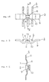
- Integrated circuit device 1 of an embodiment of the present invention includes pellet 2 of an integrated circuit formed from a semiconductor circuit as shown in Figs. 1a to 1c. This pellet 2 is mounted on radiating plate 3 in the form of an island made of a metal.
- Pellet 2 includes a large number of connection pads 4. Radiating plate 3 has a large number of lead terminals 5 arranged on the opposite sides thereof.
- connection pads 4 of pellet 2 and inner portions 6 of the large number of lead terminals 5 are individually connected to each other by a large number of bonding wires 7.
- Pellet 2, part of radiating plate 3, bonding wires 7 and inner portions 6 of lead terminals 5 are encapsulated in the inside of resin member 8.
- radiating plate 3 is formed in a shape of an arch wherein both end portions 9 thereof are positioned higher than central portion 10 thereof.
- An upper face of central portion 10 of radiating plate 3 is exposed to the top of resin member 8, and both end portions 9 are exposed to the outside from the bottom of both end portions of resin member 8.
- Pellet 2 is disposed such that also connection pads 4 are positioned on a lower face thereof. Pellet 2 is carried on a lower face of central portion 10 of radiating plate 3.
- Lead terminals 5 are formed each in a shape of a crank. While outer portions 11 of lead terminals 5 which extend outwardly from resin member 8 are positioned flush with the bottom face of resin member 8, inner portions 6 are positioned higher than outer portions 11. Also bonding wires 7 connect connection pads 4 on the lower face of pellet 2 and the lower faces of inner portions 6 of lead terminals 5 to each other.
- Integrated circuit device 1 of the present embodiment having the construction described above is mounted on an upper face of a circuit board (not shown).
- outer portions 11 of the large number of lead terminals 5 which extend outwardly from the side faces of resin member 8 are individually connected to a large number of signal lines of the circuit board by solder.
- Both end portions 9 of radiating plate 3 which extend outwardly from the front face and the rear face of resin member 8 are connected to conductor patterns such as grounding lines of the circuit board by solder.
- heat sink 12 formed as a separate member is adhered to central portion 10 of radiating plate 3, which is exposed to the top of resin member 8, by a heat conducting bonding agent such as silver paste or gold tin.
- central portion 10 of radiating plate 3 of integrated circuit device 1 to a central portion of another radiating plate (not shown) of a size larger than resin member 8 and secure the radiating plate at both end portions thereof to a circuit board by means of screws.
- integrated circuit device 1 of the present embodiment can execute various signal processes since pellet 2 can input and/or output various signals to and/or from signal lines of the circuit board through lead terminals 5.
- both end portions 9 of radiating plate 3 having pellet 2 mounted at central portion 10 thereof are exposed to the lower face of resin member 8. Since both end portions 9 are connected directly to conductor patterns of the circuit board by solder, heat generated by pellet 2 can be radiated efficiently from both end portions 9 of radiating plate 3.
- central portion 10 of radiating plate 3 on which pellet 2 is carried is exposed to the top of resin member 8. Since heat sink 12 is mounted on this central portion 10, heat generated by pellet 2 can be radiated efficiently also from central portion 10 of radiating plate 3.
- pellet 2 is disposed in a vertically inverted condition in order to realize such heat radiation from central portion 10 of radiating plate 3 as described above, since bonding wires 7 connect connection pads 4 on the lower face of pellet 2 and the lower faces of inner portions 6 of lead terminals 5 to each other, this connection is easy.
- a lead frame including a large number of lead terminals 5 and a single radiating plate 3 which are integrally connected to each other by tie bars is formed by etching of a very thin metal plate.
- this lead frame is deformed by a press machine to shape radiating plate 3 so as to have a shape of an arch as seen in Fig. 3b wherein central portion 10 is positioned higher than both end portions 9 and to shape lead terminals 5 each into a crank shape so that inner portions 6 may be positioned higher than outer portions 11 thereof.
- central portion 10 of radiating plate 3 is positioned lower than both end portions 9 and inner portions 6 of lead terminals 5 are positioned lower than outer portions 11.
- pellet 2 is mounted onto the lower face of central portion 10 of radiating plate 3 with connection pads 4 thereof positioned downwardly as seen in Fig. 4, and connection pads 4 on the lower face of pellet 2 and the lower faces of inner portions 6 of lead terminals 5 are connected to each other by bonding wires 7 as shown in Figs. 5a to 5c.
- the lead frame on which pellet 2 and inner portions 6 are mounted integrally in this manner is placed into a cavity of a pair of mutually removable metal molds.
- the lead frame is placed such that outer portions 11 of lead terminals 5 and both end portions 9 of radiating plate 3 are held by and between the pair of metal molds and the upper face of central portion 10 of radiating plate 3 is contacted with the inner face of the metal molds so that those portions may be exposed to resin member 8.
- heat sink 12 is mounted on central portion 10 of radiating plate 3 which is exposed to resin member 8 to improve the effect of heat radiation.
- central portion 10 of radiating plate 3 it is otherwise possible, for example, to cause central portion 10 of radiating plate 3 to radiate heat immediately from the surface thereof without making use of such heat sink 12 as described above.
Landscapes
- Physics & Mathematics (AREA)
- Condensed Matter Physics & Semiconductors (AREA)
- General Physics & Mathematics (AREA)
- Engineering & Computer Science (AREA)
- Computer Hardware Design (AREA)
- Microelectronics & Electronic Packaging (AREA)
- Power Engineering (AREA)
- Lead Frames For Integrated Circuits (AREA)
- Structures Or Materials For Encapsulating Or Coating Semiconductor Devices Or Solid State Devices (AREA)
- Cooling Or The Like Of Semiconductors Or Solid State Devices (AREA)
- Encapsulation Of And Coatings For Semiconductor Or Solid State Devices (AREA)
Claims (13)
- Dispositif semi-conducteur, comprenant :une pastille (2) incluant un circuit semi-conducteur comportant, disposés sur lui, une pluralité de plages de connexion (4) ;une pluralité de bornes de sortie (5) formées chacune à partir d'une plaque conductrice allongée et disposées sur le côté extérieur de ladite pastille ;une plaque rayonnante (3) formée selon une forme telle que sa partie centrale (10) est positionnée en étant plus haute que ses deux parties d'extrémité (9), en ayant ladite pastille montée sur une face inférieure de ladite partie centrale ;une pluralité de fils de connexion (7) pour connecter individuellement ladite pluralité de bornes de sortie et ladite pluralité de plages de connexion de ladite pastille, les unes aux autres ; etun élément de résine (8) pour y encapsuler ladite pastille, lesdits fils de connexion et des parties intérieures (6) desdites bornes de sortie, et encapsuler ladite plaque rayonnante de telle manière qu'une face supérieure de ladite partie centrale peut être exposée vers l'extérieur.
- Dispositif semi-conducteur selon la revendication 1, dans lequel les deux parties d'extrémité de ladite plaque rayonnante (3) sont exposées aux faces inférieures des deux parties d'extrémité dudit élément de résine.
- Dispositif semi-conducteur selon la revendication 1, dans lequel lesdits fils de connexion (7) connectent lesdites plages de connexion (4) sur une face inférieure de ladite pastille (2) et des faces inférieures desdites parties intérieures (6) desdites bornes de sortie (5), les uns aux autres.
- Dispositif semi-conducteur selon la revendication 2, dans lequel lesdits fils de connexion (7) connectent lesdites plages de connexion (4) sur une face inférieure de ladite pastille (2) et des faces inférieures des parties intérieures (6) desdites bornes de sortie (5), les uns aux autres.
- Dispositif semi-conducteur selon la revendication 3, dans lequel lesdites bornes de sortie (5) sont formées selon une forme telle que leurs parties extérieures (11) sont positionnées en étant de niveau avec la face inférieure dudit élément de résine (8) et leurs parties intérieures (6) sont positionnées en étant plus hautes que les parties extérieures (11).
- Dispositif semi-conducteur selon la revendication 4, dans lequel lesdites bornes de sortie (5) sont formées selon une forme telle que leurs parties extérieures (11) sont positionnées de niveau avec la face inférieure dudit élément de résine (8) et que leurs parties intérieures (6) sont positionnées en étant plus hautes que les parties extérieures (11).
- Dispositif semi-conducteur selon la revendication 1, dans lequel un puits de chaleur (12) est disposé sur la face supérieure de ladite partie centrale (10) de ladite plaque rayonnante (3) qui est exposée audit élément de résine (8).
- Dispositif semi-conducteur selon la revendication 2, dans lequel un puits de chaleur (12) est disposé sur la face supérieure de ladite partie centrale (10) de ladite plaque rayonnante (3) qui est exposée audit élément de résine (8).
- Dispositif semi-conducteur selon la revendication 3, dans lequel un puits de chaleur (12) est disposé sur la face supérieure de ladite partie centrale (10) de ladite plaque rayonnante (3) qui est exposée audit élément de résine (8).
- Dispositif semi-conducteur selon la revendication 4, dans lequel un puits de chaleur (12) est disposé sur la face supérieure de ladite partie centrale (10) de ladite plaque rayonnante (3) qui est exposée audit élément de résine (8).
- Dispositif semi-conducteur selon la revendication 5, dans lequel un puits de chaleur (12) est disposé sur la face supérieure de ladite partie centrale (10) de ladite plaque rayonnante (3) qui est exposée audit élément de résine (8).
- Dispositif semi-conducteur selon la revendication 6, dans lequel un puits de chaleur (12) est disposé sur la face supérieure de ladite partie centrale (10) de ladite plaque rayonnante (3) qui est exposée audit élément de résine (8).
- Procédé de fabrication d'un dispositif semi-conducteur, comprenant les étapes consistant à :former un cadre conducteur dans lequel une plaque rayonnante (3) formée selon une forme telle que sa partie centrale (10) est positionnée en étant plus haute que ses deux parties d'extrémité (9), et une pluralité de bornes de sortie (5) formées selon une forme telle que leurs parties intérieures (6) sont positionnées en étant plus hautes que leurs parties extérieures (11), sont connectées d'un seul tenant les unes aux autres par des éléments de support ;monter une pastille (2) incluant un circuit semi-conducteur comportant, disposés sur lui, une pluralité de plages de connexion (4), sur une face inférieure d'une partie de la plaque rayonnante (3) du cadre conducteur dans une condition telle que les plages de connexion (4) sont positionnés vers le bas ;connecter la pluralité de plages de connexion (4) de la pastille (2) montée sur le cadre conducteur et les faces inférieures des parties intérieures (6) de la pluralité de bornes de sortie (5) individuellement les uns aux autres par une pluralité de fils de connexion (7) ;placer au moins la pastille (2) et les fils de connexion (7) dans une cavité d'au moins une paire de moules métalliques mutuellement amovibles de telle sorte que les deux parties d'extrémité (9) de la plaque rayonnante (3) du cadre conducteur et les parties extérieures (11) des bornes de sortie (5) sont tenues par et entre lesdits moules métalliques, et une face supérieure de la partie centrale (10) de la plaque rayonnante (3) est mise au contact d'une face intérieure desdits moules métalliques ;verser une résine fondue dans la cavité desdits moules métalliques ;laisser la résine versée dans la cavité desdits moules métalliques jusqu'à ce que la résine soit solidifiée pour former un élément de résine (8) dans lequel au moins une partie de la plaque rayonnante (3), de la pastille (2), des fils de connexion (7) et des parties intérieures (6) des bornes de sortie (5) sont encapsulés et à partir desquels les parties extérieures (11) des bornes de sortie (5) sont exposées vers l'extérieur ; etdécouper les éléments de support du cadre conducteur pour séparer individuellement, les unes des autres, la plaque rayonnante (3) et la pluralité de bornes de sortie (5).
Applications Claiming Priority (2)
| Application Number | Priority Date | Filing Date | Title |
|---|---|---|---|
| JP128758/97 | 1997-05-19 | ||
| JP9128758A JP2907186B2 (ja) | 1997-05-19 | 1997-05-19 | 半導体装置、その製造方法 |
Publications (3)
| Publication Number | Publication Date |
|---|---|
| EP0880176A2 EP0880176A2 (fr) | 1998-11-25 |
| EP0880176A3 EP0880176A3 (fr) | 1999-01-20 |
| EP0880176B1 true EP0880176B1 (fr) | 2006-12-20 |
Family
ID=14992744
Family Applications (1)
| Application Number | Title | Priority Date | Filing Date |
|---|---|---|---|
| EP98108897A Expired - Lifetime EP0880176B1 (fr) | 1997-05-19 | 1998-05-15 | Dispositif semiconducteur avec pastille montée sur une plaque de radiation |
Country Status (7)
| Country | Link |
|---|---|
| US (1) | US6242797B1 (fr) |
| EP (1) | EP0880176B1 (fr) |
| JP (1) | JP2907186B2 (fr) |
| KR (1) | KR100328746B1 (fr) |
| CN (1) | CN1110089C (fr) |
| DE (1) | DE69836652T2 (fr) |
| TW (1) | TW402797B (fr) |
Families Citing this family (19)
| Publication number | Priority date | Publication date | Assignee | Title |
|---|---|---|---|---|
| JP3003638B2 (ja) * | 1997-08-05 | 2000-01-31 | 日本電気株式会社 | 半導体装置、その製造方法 |
| JP3339838B2 (ja) * | 1999-06-07 | 2002-10-28 | ローム株式会社 | 半導体装置およびその製造方法 |
| JP2002026044A (ja) * | 2000-07-05 | 2002-01-25 | Seiko Epson Corp | 半導体装置及びその製造方法、回路基板並びに電子機器 |
| US6392288B1 (en) * | 2000-12-04 | 2002-05-21 | Semiconductor Components Industries Llc | Lead frame for assembly for thin small outline plastic encapsulated packages |
| US6469398B1 (en) * | 2001-03-29 | 2002-10-22 | Kabushiki Kaisha Toshiba | Semiconductor package and manufacturing method thereof |
| US7057273B2 (en) | 2001-05-15 | 2006-06-06 | Gem Services, Inc. | Surface mount package |
| JP3580293B2 (ja) * | 2002-03-26 | 2004-10-20 | 株式会社デンソー | 半導体装置の製造方法 |
| JP2003224239A (ja) * | 2002-01-29 | 2003-08-08 | Sanyo Electric Co Ltd | 半導体装置およびその製造方法 |
| US6992503B2 (en) * | 2002-07-08 | 2006-01-31 | Viciciv Technology | Programmable devices with convertibility to customizable devices |
| EP1473763A1 (fr) * | 2003-04-30 | 2004-11-03 | STMicroelectronics S.r.l. | Méthode de fabrication d'une grille de connections pour des dispositifs semi-conducteurs de puissance, dans laquelle en une étape les connections sont séparées et la plage de puce est poussée en bas |
| JP2004349347A (ja) | 2003-05-20 | 2004-12-09 | Rohm Co Ltd | 半導体装置 |
| US6979900B2 (en) * | 2003-10-21 | 2005-12-27 | Delphi Technologies, Inc. | Integrated circuit package with integral leadframe convector and method therefor |
| TWM260864U (en) * | 2004-07-23 | 2005-04-01 | Fen Te Co Ltd | Transistor for stable chip mounting |
| US7851268B2 (en) * | 2005-04-09 | 2010-12-14 | Stats Chippac Ltd. | Integrated circuit package system using heat slug |
| JP5103731B2 (ja) * | 2005-12-12 | 2012-12-19 | 三菱電機株式会社 | モールドパッケージ |
| KR101473027B1 (ko) * | 2007-02-02 | 2014-12-15 | 디에스엠 아이피 어셋츠 비.브이. | 열 전달 어셈블리 |
| JP2009044081A (ja) * | 2007-08-10 | 2009-02-26 | Rohm Co Ltd | 駆動装置 |
| US10938303B2 (en) | 2007-08-10 | 2021-03-02 | Rohm Co., Ltd. | Driving device |
| US7875970B2 (en) * | 2009-06-10 | 2011-01-25 | Green Arrow Asia Limited | Integrated circuit package having a castellated heatspreader |
Family Cites Families (30)
| Publication number | Priority date | Publication date | Assignee | Title |
|---|---|---|---|---|
| JPS6020943Y2 (ja) * | 1979-08-29 | 1985-06-22 | 三菱電機株式会社 | 半導体装置 |
| JPS5943534A (ja) * | 1982-09-02 | 1984-03-10 | Mitsubishi Electric Corp | 半導体装置の製造方法 |
| JPS60238839A (ja) | 1984-05-14 | 1985-11-27 | Ricoh Co Ltd | 電子写真製版用印刷原版 |
| JPS60257159A (ja) * | 1984-06-01 | 1985-12-18 | Nec Corp | 半導体装置 |
| JPS61216454A (ja) | 1985-03-22 | 1986-09-26 | Toshiba Corp | 樹脂封止型半導体装置 |
| JPS6297358A (ja) * | 1985-10-23 | 1987-05-06 | Mitsubishi Electric Corp | 樹脂封止形半導体集積回路装置 |
| JPH01132142A (ja) * | 1987-08-05 | 1989-05-24 | Mitsubishi Electric Corp | 半導体装置のパツケージ構造 |
| US5157478A (en) * | 1989-04-19 | 1992-10-20 | Mitsubishi Denki Kabushiki Kaisha | Tape automated bonding packaged semiconductor device incorporating a heat sink |
| DE69033226T2 (de) | 1989-12-12 | 2000-02-17 | Sumitomo Special Metals Co., Ltd. | Wärmeleitendes Mischmaterial |
| JP2979637B2 (ja) * | 1990-11-30 | 1999-11-15 | 日本電気株式会社 | 半導体装置 |
| IT1250405B (it) * | 1991-01-31 | 1995-04-07 | Sgs Thomson Microelectronics | Piastrina metallica di dissipazione del calore di un dispositivo a semiconduttore di potenza incapsulato in resina fornita di rilievi per la saldatura dei fili di massa |
| JPH04291948A (ja) * | 1991-03-20 | 1992-10-16 | Fujitsu Ltd | 半導体装置及びその製造方法及び放熱フィン |
| JPH04326556A (ja) | 1991-04-25 | 1992-11-16 | Sony Corp | 樹脂封止型半導体装置 |
| US5281849A (en) * | 1991-05-07 | 1994-01-25 | Singh Deo Narendra N | Semiconductor package with segmented lead frame |
| JPH0557542A (ja) | 1991-08-30 | 1993-03-09 | Canon Inc | 電動ドライバーの給電方法 |
| US5225897A (en) * | 1991-10-02 | 1993-07-06 | Unitrode Corporation | Molded package for semiconductor devices with leadframe locking structure |
| JP2995119B2 (ja) * | 1992-02-17 | 1999-12-27 | アピックヤマダ株式会社 | パワートランジスタ用リードフレームの製造方法 |
| US5289344A (en) * | 1992-10-08 | 1994-02-22 | Allegro Microsystems Inc. | Integrated-circuit lead-frame package with failure-resistant ground-lead and heat-sink means |
| JPH06209054A (ja) | 1993-01-08 | 1994-07-26 | Mitsubishi Electric Corp | 半導体装置 |
| JPH06224326A (ja) | 1993-01-21 | 1994-08-12 | Nippon Steel Corp | 放熱器及びこの放熱器を用いた半導体パッケージ |
| JPH06275759A (ja) | 1993-03-17 | 1994-09-30 | Fujitsu Ltd | 半導体装置及びその製造方法 |
| KR960000706B1 (ko) | 1993-07-12 | 1996-01-11 | 한국전기통신공사 | 전력소자용 플라스틱 패키지 구조 및 그 제조방법 |
| JPH0786458A (ja) * | 1993-09-09 | 1995-03-31 | Fujitsu Ltd | 半導体装置及びその製造方法 |
| JPH07335980A (ja) * | 1994-06-07 | 1995-12-22 | Fuji Electric Co Ltd | 半導体レーザ装置 |
| JPH08111491A (ja) * | 1994-10-12 | 1996-04-30 | Toshiba Corp | 半導体装置 |
| JPH08181266A (ja) | 1994-12-21 | 1996-07-12 | Hitachi Ltd | リードフレームおよびそれを用いて構成された半導体装置 |
| US5929517A (en) * | 1994-12-29 | 1999-07-27 | Tessera, Inc. | Compliant integrated circuit package and method of fabricating the same |
| JPH09199645A (ja) * | 1996-01-17 | 1997-07-31 | Mitsubishi Electric Corp | 半導体装置および半導体モジュール |
| US5939781A (en) * | 1996-09-26 | 1999-08-17 | Texas Instruments Incorporated | Thermally enhanced integrated circuit packaging system |
| US5917704A (en) * | 1997-10-06 | 1999-06-29 | Ford Motor Company | Laser-solderable electronic component |
-
1997
- 1997-05-19 JP JP9128758A patent/JP2907186B2/ja not_active Expired - Fee Related
-
1998
- 1998-04-13 US US09/059,324 patent/US6242797B1/en not_active Expired - Lifetime
- 1998-04-16 TW TW087105941A patent/TW402797B/zh not_active IP Right Cessation
- 1998-05-08 CN CN98101785A patent/CN1110089C/zh not_active Expired - Fee Related
- 1998-05-11 KR KR1019980016763A patent/KR100328746B1/ko not_active IP Right Cessation
- 1998-05-15 DE DE69836652T patent/DE69836652T2/de not_active Expired - Fee Related
- 1998-05-15 EP EP98108897A patent/EP0880176B1/fr not_active Expired - Lifetime
Also Published As
| Publication number | Publication date |
|---|---|
| EP0880176A2 (fr) | 1998-11-25 |
| DE69836652T2 (de) | 2007-09-27 |
| TW402797B (en) | 2000-08-21 |
| US6242797B1 (en) | 2001-06-05 |
| KR100328746B1 (ko) | 2002-05-09 |
| JP2907186B2 (ja) | 1999-06-21 |
| JPH10321768A (ja) | 1998-12-04 |
| CN1110089C (zh) | 2003-05-28 |
| KR19980086923A (ko) | 1998-12-05 |
| DE69836652D1 (de) | 2007-02-01 |
| EP0880176A3 (fr) | 1999-01-20 |
| CN1200567A (zh) | 1998-12-02 |
Similar Documents
| Publication | Publication Date | Title |
|---|---|---|
| EP0880176B1 (fr) | Dispositif semiconducteur avec pastille montée sur une plaque de radiation | |
| US6319753B1 (en) | Semiconductor device having lead terminals bent in J-shape | |
| KR100294719B1 (ko) | 수지밀봉형 반도체장치 및 그 제조방법, 리드프레임 | |
| US8659146B2 (en) | Lead frame based, over-molded semiconductor package with integrated through hole technology (THT) heat spreader pin(s) and associated method of manufacturing | |
| US20020027297A1 (en) | Semiconductor package | |
| JP3027954B2 (ja) | 集積回路装置、その製造方法 | |
| JP2001313363A (ja) | 樹脂封止型半導体装置 | |
| US6617200B2 (en) | System and method for fabricating a semiconductor device | |
| EP0880178B1 (fr) | Méthode de fabrication d'un dispositif semiconducteur avec une paire de terminaisons à rayonnement et une multiplicité de connexions externes formées à partir d'une seule grille de connexion | |
| US6150715A (en) | Semiconductor device with radiation plate for high radiation character and method of manufacturing the same | |
| JPH11330314A (ja) | 半導体装置の製造方法及びその構造、該方法に用いるリードフレーム | |
| JP3061120B2 (ja) | 半導体装置、その製造方法 | |
| JP2819282B2 (ja) | 半導体パッケージおよびその製造方法 | |
| JP2976941B2 (ja) | 半導体装置、その製造方法 | |
| WO2021195903A1 (fr) | Système sous boîtier et dispositif électronique | |
| KR100342811B1 (ko) | 복수개의칩이내장된에어리어어레이범프드반도체패키지 | |
| JPH06163760A (ja) | 放熱スラグを有した電子部品搭載用基板 | |
| JPH06112400A (ja) | 半導体装置 |
Legal Events
| Date | Code | Title | Description |
|---|---|---|---|
| PUAI | Public reference made under article 153(3) epc to a published international application that has entered the european phase |
Free format text: ORIGINAL CODE: 0009012 |
|
| AK | Designated contracting states |
Kind code of ref document: A2 Designated state(s): DE FR GB |
|
| AX | Request for extension of the european patent |
Free format text: AL;LT;LV;MK;RO;SI |
|
| PUAL | Search report despatched |
Free format text: ORIGINAL CODE: 0009013 |
|
| AK | Designated contracting states |
Kind code of ref document: A3 Designated state(s): AT BE CH CY DE DK ES FI FR GB GR IE IT LI LU MC NL PT SE |
|
| AX | Request for extension of the european patent |
Free format text: AL;LT;LV;MK;RO;SI |
|
| 17P | Request for examination filed |
Effective date: 19990317 |
|
| AKX | Designation fees paid |
Free format text: DE FR GB |
|
| RAP1 | Party data changed (applicant data changed or rights of an application transferred) |
Owner name: NEC COMPOUND SEMICONDUCTOR DEVICES, LTD. |
|
| RAP1 | Party data changed (applicant data changed or rights of an application transferred) |
Owner name: NEC ELECTRONICS CORPORATION |
|
| GRAP | Despatch of communication of intention to grant a patent |
Free format text: ORIGINAL CODE: EPIDOSNIGR1 |
|
| GRAS | Grant fee paid |
Free format text: ORIGINAL CODE: EPIDOSNIGR3 |
|
| GRAA | (expected) grant |
Free format text: ORIGINAL CODE: 0009210 |
|
| AK | Designated contracting states |
Kind code of ref document: B1 Designated state(s): DE FR GB |
|
| REG | Reference to a national code |
Ref country code: GB Ref legal event code: FG4D |
|
| REF | Corresponds to: |
Ref document number: 69836652 Country of ref document: DE Date of ref document: 20070201 Kind code of ref document: P |
|
| ET | Fr: translation filed | ||
| PLBE | No opposition filed within time limit |
Free format text: ORIGINAL CODE: 0009261 |
|
| STAA | Information on the status of an ep patent application or granted ep patent |
Free format text: STATUS: NO OPPOSITION FILED WITHIN TIME LIMIT |
|
| 26N | No opposition filed |
Effective date: 20070921 |
|
| PGFP | Annual fee paid to national office [announced via postgrant information from national office to epo] |
Ref country code: FR Payment date: 20090515 Year of fee payment: 12 Ref country code: DE Payment date: 20090511 Year of fee payment: 12 |
|
| PGFP | Annual fee paid to national office [announced via postgrant information from national office to epo] |
Ref country code: GB Payment date: 20090513 Year of fee payment: 12 |
|
| GBPC | Gb: european patent ceased through non-payment of renewal fee |
Effective date: 20100515 |
|
| REG | Reference to a national code |
Ref country code: FR Ref legal event code: ST Effective date: 20110131 |
|
| PG25 | Lapsed in a contracting state [announced via postgrant information from national office to epo] |
Ref country code: DE Free format text: LAPSE BECAUSE OF NON-PAYMENT OF DUE FEES Effective date: 20101201 |
|
| PG25 | Lapsed in a contracting state [announced via postgrant information from national office to epo] |
Ref country code: FR Free format text: LAPSE BECAUSE OF NON-PAYMENT OF DUE FEES Effective date: 20100531 |
|
| PG25 | Lapsed in a contracting state [announced via postgrant information from national office to epo] |
Ref country code: GB Free format text: LAPSE BECAUSE OF NON-PAYMENT OF DUE FEES Effective date: 20100515 |