EP0844616B1 - Semiconductor memory device - Google Patents
Semiconductor memory device Download PDFInfo
- Publication number
- EP0844616B1 EP0844616B1 EP98101289A EP98101289A EP0844616B1 EP 0844616 B1 EP0844616 B1 EP 0844616B1 EP 98101289 A EP98101289 A EP 98101289A EP 98101289 A EP98101289 A EP 98101289A EP 0844616 B1 EP0844616 B1 EP 0844616B1
- Authority
- EP
- European Patent Office
- Prior art keywords
- column
- data
- lines
- units
- select
- Prior art date
- Legal status (The legal status is an assumption and is not a legal conclusion. Google has not performed a legal analysis and makes no representation as to the accuracy of the status listed.)
- Expired - Lifetime
Links
Images


Classifications
-
- G—PHYSICS
- G11—INFORMATION STORAGE
- G11C—STATIC STORES
- G11C7/00—Arrangements for writing information into, or reading information out from, a digital store
- G11C7/10—Input/output [I/O] data interface arrangements, e.g. I/O data control circuits, I/O data buffers
- G11C7/1051—Data output circuits, e.g. read-out amplifiers, data output buffers, data output registers, data output level conversion circuits
-
- G—PHYSICS
- G11—INFORMATION STORAGE
- G11C—STATIC STORES
- G11C7/00—Arrangements for writing information into, or reading information out from, a digital store
- G11C7/10—Input/output [I/O] data interface arrangements, e.g. I/O data control circuits, I/O data buffers
- G11C7/1006—Data managing, e.g. manipulating data before writing or reading out, data bus switches or control circuits therefor
-
- G—PHYSICS
- G11—INFORMATION STORAGE
- G11C—STATIC STORES
- G11C7/00—Arrangements for writing information into, or reading information out from, a digital store
- G11C7/10—Input/output [I/O] data interface arrangements, e.g. I/O data control circuits, I/O data buffers
- G11C7/1015—Read-write modes for single port memories, i.e. having either a random port or a serial port
- G11C7/103—Read-write modes for single port memories, i.e. having either a random port or a serial port using serially addressed read-write data registers
-
- G—PHYSICS
- G11—INFORMATION STORAGE
- G11C—STATIC STORES
- G11C7/00—Arrangements for writing information into, or reading information out from, a digital store
- G11C7/10—Input/output [I/O] data interface arrangements, e.g. I/O data control circuits, I/O data buffers
- G11C7/1072—Input/output [I/O] data interface arrangements, e.g. I/O data control circuits, I/O data buffers for memories with random access ports synchronised on clock signal pulse trains, e.g. synchronous memories, self timed memories
Definitions
- the present invention relates to a semiconductor memory device, and more specifically to a semiconductor memory device suitable for a clock-synchronous random access memory which can output data at high speed and at random.
- a microprocessor is provided with a primary memory device of a large capacity.
- a memory device capable of accessing data at high speed at the sacrifice of random characteristics of data access, in order to solve a bottleneck with respect to low processing speed due of the low access speed of the external memory device.
- Japanese Patent Publication No. 5-2873 January 8, 1993
- Japanese Patent Publication No. 6-84351 discloses a memory device provided with internal data registers, which operates as follows: a group of access data are stored in the internal registers temporarily for data access between the outside and the memory cells.
- the data to be stored in the registers are selected by scrambler circuits; that is, a scrambler control circuit controls the scrambler circuits so that access data can be stored cyclically in the respective registers at predetermined sequence for each cycle of a clock signal. Further, the data are inputted and outputted between the outside and the registers via an input/output buffer. In response to a head address indicative of data access start, a predetermined selection sequence of the scrambler circuits is determined.
- a column decoder 1 selects one of cell blocks CB1 to CB5 of a memory core 2.
- Each of the cell blocks CB1 to CB5 includes 4 columns CM1 to CM4.
- Data stored in the four columns CM1 to CM4 of one of the cell blocks CB1 to CB5 are outputted to data lines DLN simultaneously.
- the data on the data lines DLN are transferred to read/write data lines RWD via a data buffer 4.
- the read/write data lines RWD are connected to data registers 51 and 52 via scrambler circuits 61 and 62, respectively.
- a scrambler control circuit 7 controls the two scrambler circuits 61 and 62 so that the data on the read/write data line RWD can be selectively stored 2 bits by 2 bits in data areas R1, R2, R3 and R4 of the data registers 51 and 52, respectively.
- the data stored in the data registers 51 and 52 are selected by a data selection section 9 and then outputted through a data output buffer 8 as data output.
- One block of the five cell blocks CB1 to CB5 of the memory cell 2 is selected by the column decoder 1.
- Data of the four columns CM1 to CM4 of the selected block are read simultaneously to the data lines DLN, and then transferred to the read/write data lines RWD via the data buffer 4.
- the four bit data are selectively stored 2 bits by 2 bits in the data areas R1, R2, R3 and R4 of the data registers 51 and 52, respectively via the scrambler circuits 61 and 62 controlled by the scrambler control circuit 7.
- the access sequence of the data areas R1, R2, R3 and R4 of the data registers 51 and 52 is as follows: R1, R2, R3 and R4.
- the data stored in the data areas R1, R2, R3 and R4 are selected by the data selector section 9, transferred to the data output buffer 8, and then outputted therefrom as the data output.
- DE-A-41 18 804 discloses a dynamic semiconductor memory device having an MOS memory arrangement comprising an array of memory cells arranged in rows and columns. The rows of memory cells are connected to word lines. Pairs of bit lines connected to the columns are also provided. Sense amplifiers and transfer gates are provided for each pair of bit lines. A row decoder is connected to transfer gates via row selection lines in such a way that each output of the row decoder is connected to two adjacent transfer gates. When activating a specific column, the row decoder activates another column next to the specific column, before the specific column address is actually received. As a consequence, information bits stored in four memory cells can simultaneously be transferred to registers and held therein. A multiplexer performs the serial read out of the held information bits.
- the object of the present invention is to provide an improved clock-synchronism semiconductor memory device high in access speed, by which data of column bits more than the number of registers can be accessed continuously, in spite of the minimum number of registers, and further the column address from which the access starts can be selected freely.
- column data more than the number of the data registers arranged on the output side can be accessed continuously, irrespective of the number of the data registers directly, and further any access start address can be determined.
- Fig. 1 is a block diagram showing one embodiment of the semiconductor memory device according to the present invention.
- a memory cell array MCA includes a plurality of memory cells arranged in matrix pattern.
- decode signals are applied from a row decoder RD.
- columns b11, b12, b21, b22, b31, b32, b41, b42, ...., b(n/2)1, b(n/2)2 which constitute the memory cell array 1 have a pair of complementary bit lines, respectively. Data on the bit lines can be read by sensing the bit line data by sense amplifiers.
- the columns b11, b12, b21, b22, b31, b32, b41, b42, ...., b(n/2)1, b(n/2)2 are connected to column gates 11, 12, 13, 14, 15, 16, 17, 18, ..., 1n-1, 1n, respectively.
- the column gates 11 to 1n are turned on or off by column select lines C1 to Cn/2, respectively. Two of the column select lines are selected by a column gate group selection circuit CGS. Two column gates are turned on by the single selected column select line.
- Data on the columns b11, b12, ..., b(n/2)1, b(n/2)2 are transmitted to data lines DLN through the column gates 11 to 1n.
- a scrambler control circuit 10 controls scrambler circuits 61 and 62, and further selects two column select lines C1 to Cn/2 through the column gate group selection circuit CGS. To the scrambler control circuit 10, a read address A READ is applied.
- two of the column select lines C1 to Cn/2 are activated simultaneously by the scrambler control circuit 10.
- four of the column gates 11 to 1n can be selected, so that 4-bit data are outputted from the four columns to the data lines DLN.
- the column select lines C1 to Cn/2 are selected in such a way that a plurality of the data are not outputted to the same data lines DLN for prevention of data interference.
- the column select lines C1 and C3 are not selected simultaneously.
- the 4-bit data transferred to the data line DLN are amplified by the data buffer 4, and then transferred to the read/write data lines RWD.
- Two bits of each of the 4-bit data transferred to the read/write lines RWD as described above are selected by the scrambler circuits 61 and 62, respectively, and then stored in data areas R1 and R2 of a data register 51 or in data areas R3 and R4 of a data register 52, respectively under control of the scrambler control circuit 10 to the scrambler circuits 61 and 62.
- the data in the areas R1, R2, R3 and R4 of the data registers 51 and 52 are selected by a data selection section 9, and then outputted to the outside through a data output buffer 8 as data output.
- Fig. 2 is a timing chart which shows the above-mentioned operation in sequence with respect to time.
- A indicates a basic clock CLK
- B indicates a column address select signal /CAS
- C indicates data including data to be stored in the data areas R1/R2, respectively
- D indicates a timing at which data are stored in the data areas R1/R2, respectively
- E indicates a timing at which data are stored in the data areas R3/R4, respectively
- F indicates data including data to be stored in the data areas R3/R4, respectively
- G (H) and (I) indicate the statuses of output 1, output 2 and output 3 derived as data output, respectively
- J indicates the statuses of the column select lines C1 to Cn/2, respectively.
- Figs. 2(C) and (F) show these deterministic data. Each of these data can be determined being transferred 4 bits by 4 bits. Two bits of the four bits are stored in the data registers 51 and 52, respectively. Therefore, in Fig. 2, data are shown for each data register 51 or 52.
- Fig. 2 (C) shows 4-bit data including 2-bit data to be stored in the data areas R1 and R2 of the data register 51.
- FIG. 2 (F) shows 4-bit data including 2-bit data to be stored in the data areas R3 and R4 of the data register 52.
- the data output 1 can be obtained from an address determined in response to the clock CLK "1" as follows:
- the column address select lines C1 to Cn/2 including the determined head address and the column address select lines C1 to Cn/2 adjacent thereto in the output sequence direction are selectively activated under control of the scrambler control circuit 10. Consequently, the corresponding column gates 11, 12, 13, ..., 1n are selected, so that 4-bit data are outputted to the data lines DLN.
- These data are sensed by the data buffer 4 to determine the read/write data line RWD, as shown in Fig. 2(C).
- Data which constitute the first two bits of the 4-bit output 1 are stored in the data areas R1 and R2 through the scrambler circuit 61, at the timing as shown in Fig. 2(D).
- Fig. 2(F) shows the status in which the data are read to the data lines DLN and further determined by the read/write data lines RWD.
- the third and fourth bits of the 4-bit output 1 determined as described above are stored in the data areas R3 and R4 of the data register 52 through the scrambler circuit 62, as shown in Fig. 2(E). The similar operation is repeated in sequence for each two cycles of the clock CLK.
- the data stored in the data registers 51 and 52 are accessed in the sequence of the data areas R1, R2, R3 and R4 as shown over the clock CLK in Fig. 2(A). After having been transferred to the read/write data lines RWD, the data are stored in the data registers 51 and 52 in accordance with the address sequence expected by the scrambler control circuit 10. Therefore, it is possible to output the data in the expected sequence. On the other hand, when the head address of a series of the data is determined again, the data can be outputted as the output 2 or the output 3, as shown in Figs. 2(H) and (I), respectively.
- a new head address of the output 3 is determined.
- the data of the output 3 are outputted beginning from the data area R3 of the data register 52.
- the sequence of the data transfer is the same as with the case of the outputs 1 and 2.
- the new head address is determined at the row of the clock CLK "11".
- the 4-bit data including the head address are determined on the read/write data lines RWD, as shown by B in Fig. 2(F).
- the 2 bits of the 4-bit data are selected by the scrambler circuit 62, and stored in the data areas R3 and R4 of the data register 52 at the timing as shown in Fig. 2(E). In the same way, the 4-bit data are transferred for each two cycles, and further 2 bits of the data are selected.
- the above-mentioned sequence is repeated to output a series of data continuously.
- the scrambler control circuit 10 selects the column select lines C1 to Cn/2 and the scrambler circuits 61 and 62, respectively in sequence as follows:
- the description will be made on condition that the column select lines C1 to C4 shown in Fig. 1 correspond to the data sequence of a series of 8-bit data.
- Table 1 lists the relationship among the eight serial and cyclic access modes classified according to the eight head address, a pair of select lines C1 to C4 to be selected, 2-bit read/write data lines RWD to be selected from the read/write data lines RWD on which the 4-bit data have been determined, and the data areas R1 to R4 of the data registers 51 and 52, respectively.
- Table 2 lists the similar relationship among the eight serial and cyclic access modes classified according to the eight head address, a pair of select lines C1 to C4 to be selected, 2-bit read/write data lines RWD to be selected from the read/write data lines RWD on which the 4-bit data have been determined, and the data areas R1 to R4 of the data registers 51 and 52, respectively SER ACCESS SEQ (a) R1 R2 R3 R4 R1 R2 R3 R4 (1) 1-2-3-4-5-6-7-8 (A) (c1,c2) (c2,c3) (c3,c4) (c4,c1) (B) 1 2 3 4 1 2 3 4 (2) 2-3-4-5-6-7-8-1 (A) (c1,c2) (c2,c3) (c3,c4) (c4,c1) (B) 2 1 4 3 2 1 4 3 (3) 3-4-5-6-7-8-1-2 (A) (c2,c1) (c1,c4) (c4,c3) (c3,c2) (B) 3 4 1 2 3 4 1 2 (4) 4-5-6-7-8-1-2-3 (A
- the selection (A) of the column select lines C1 to Cn/2 and the connection (B) of the selected read/write data lines RWD to the data areas R1, R2, R3 and R4 of the data registers 51 and 52 are both shown in the same column from the functional standpoint. However, the operational timings are different from each other. Further, the data selected and transferred through the column select lines C1 to Cn/2 are added thereafter to the data areas R1, R2, R3 and R4, as depicted by the timing chart shown in Fig. 2.
- the number of columns b11 to b(n/2)2 connected to the data lines DLN simultaneously by the column select lines C1 to Cn/2 is two. In the actual system, however, this number changes according to the time required to determined the data beginning from the columns b11 to b(n/2)2 to the read/write data lines RWD.
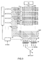
- Fig. 3 shows another embodiment of the semiconductor memory device according to the present invention, which is configured on the basis of the above-mentioned standpoint.
- two sets of the data stored in the columns b11, b23, b13, b21, b22, b23, ... are selected simultaneously 3 bits by 3 bits through the column select lines C1, C2, ... by the column gates 11, 12, 13, .... Therefore, the number of the data lines DLN and that of the read/write data lines RWD are six, respectively.
- the number of bits of the data register 51 becomes 3 bits in correspondence to the data areas R1, R2 and R3, and similarly the number of bits of the data register 52 becomes 3 bits in correspondence to the data areas R4, R5 and R6.
- two sets of the columns b11, b12 and b13; the columns b31, b32 and b33; the columns b41, 42 and 43 are selected simultaneously by the column gates 11, 12 and 13, and then outputted to the data lines DLN as 6-bit data.
- the outputted 6-bit data are transferred to the read/write data lines RWD through the data buffer 4, and further transferred to and stored in the data registers 51 and 52 3 bits by 3 bits through the scrambler circuits 61 and 62, respectively.
- the stored data can be outputted to the outside through the data buffer 8 by selecting the data areas R1, R2, R3, R4, R5 and R6 of the data registers 51 and 52 through the data selection section 9.
- the addresses are updated for each 3 cycles.
- the number of the columns selected by one column select line is a . Therefore, when two column select lines are selected simultaneously, 2a-bit data can be transferred.
- the number of output registers is 2a
- the data are selectively stored in the a -unit registers by selecting a-bit data from the 2a-bit data. As described above, it is possible to access a series of data more than the number of the output registers by selecting the two column select lines for each a cycles.
- the operation is as follows: data are transferred from the columns of a bits simultaneously by selecting one column select line. In transferring data for each a cycles, 2 a bit data are transferred by selecting two column select lines. As described above, a -bit data are stored selectively in the a -unit output registers of the 2a-unit output registers. Accordingly, since a -bit data exist always in the 2a-bit data transferred from any given address, it is possible to store data in the a -unit registers in a predetermined data access sequence for each a cycles. In other words, a new head address can be set for each a cycles and further a series of data can be accessed continuously, irrespective of the number of the data transfer lines and the data registers, thus enabling an optimum synchronous data access.
- column data more than the number of the data registers arranged on the output side can be accessed continuously, irrespective of the number of the data registers, and further any access start address can be determined.
Landscapes
- Dram (AREA)
- Static Random-Access Memory (AREA)
Priority Applications (1)
| Application Number | Priority Date | Filing Date | Title |
|---|---|---|---|
| EP02009263A EP1231606B1 (en) | 1992-08-28 | 1993-08-27 | Semiconductor device |
Applications Claiming Priority (4)
| Application Number | Priority Date | Filing Date | Title |
|---|---|---|---|
| JP230583/92 | 1992-08-28 | ||
| JP4230583A JP2825401B2 (ja) | 1992-08-28 | 1992-08-28 | 半導体記憶装置 |
| JP23058392 | 1992-08-28 | ||
| EP93113753A EP0588129B1 (en) | 1992-08-28 | 1993-08-27 | Semiconductor memory device |
Related Parent Applications (1)
| Application Number | Title | Priority Date | Filing Date |
|---|---|---|---|
| EP93113753A Division EP0588129B1 (en) | 1992-08-28 | 1993-08-27 | Semiconductor memory device |
Related Child Applications (1)
| Application Number | Title | Priority Date | Filing Date |
|---|---|---|---|
| EP02009263A Division EP1231606B1 (en) | 1992-08-28 | 1993-08-27 | Semiconductor device |
Publications (3)
| Publication Number | Publication Date |
|---|---|
| EP0844616A2 EP0844616A2 (en) | 1998-05-27 |
| EP0844616A3 EP0844616A3 (en) | 1999-05-26 |
| EP0844616B1 true EP0844616B1 (en) | 2002-10-16 |
Family
ID=16910019
Family Applications (3)
| Application Number | Title | Priority Date | Filing Date |
|---|---|---|---|
| EP98101289A Expired - Lifetime EP0844616B1 (en) | 1992-08-28 | 1993-08-27 | Semiconductor memory device |
| EP93113753A Expired - Lifetime EP0588129B1 (en) | 1992-08-28 | 1993-08-27 | Semiconductor memory device |
| EP02009263A Expired - Lifetime EP1231606B1 (en) | 1992-08-28 | 1993-08-27 | Semiconductor device |
Family Applications After (2)
| Application Number | Title | Priority Date | Filing Date |
|---|---|---|---|
| EP93113753A Expired - Lifetime EP0588129B1 (en) | 1992-08-28 | 1993-08-27 | Semiconductor memory device |
| EP02009263A Expired - Lifetime EP1231606B1 (en) | 1992-08-28 | 1993-08-27 | Semiconductor device |
Country Status (5)
| Country | Link |
|---|---|
| US (2) | US5392254A (ko) |
| EP (3) | EP0844616B1 (ko) |
| JP (1) | JP2825401B2 (ko) |
| KR (1) | KR0136747B1 (ko) |
| DE (3) | DE69332420T2 (ko) |
Families Citing this family (7)
| Publication number | Priority date | Publication date | Assignee | Title |
|---|---|---|---|---|
| US6085283A (en) * | 1993-11-19 | 2000-07-04 | Kabushiki Kaisha Toshiba | Data selecting memory device and selected data transfer device |
| JP2982618B2 (ja) * | 1994-06-28 | 1999-11-29 | 日本電気株式会社 | メモリ選択回路 |
| JP3351692B2 (ja) * | 1995-09-12 | 2002-12-03 | 株式会社東芝 | シンクロナス半導体メモリ装置 |
| JP3406790B2 (ja) | 1996-11-25 | 2003-05-12 | 株式会社東芝 | データ転送システム及びデータ転送方法 |
| JPH10188556A (ja) * | 1996-12-20 | 1998-07-21 | Fujitsu Ltd | 半導体記憶装置 |
| US6925086B2 (en) * | 2000-12-12 | 2005-08-02 | International Business Machines Corporation | Packet memory system |
| JP6239078B1 (ja) * | 2016-11-04 | 2017-11-29 | ウィンボンド エレクトロニクス コーポレーション | 半導体記憶装置および読出し方法 |
Family Cites Families (10)
| Publication number | Priority date | Publication date | Assignee | Title |
|---|---|---|---|---|
| JPS59180871A (ja) * | 1983-03-31 | 1984-10-15 | Fujitsu Ltd | 半導体メモリ装置 |
| JPH0787037B2 (ja) * | 1984-03-02 | 1995-09-20 | 沖電気工業株式会社 | 半導体メモリ回路のデータ書込方法 |
| JPS6240693A (ja) * | 1985-08-16 | 1987-02-21 | Fujitsu Ltd | ニブル・モ−ド機能を有する半導体記憶装置 |
| JPH0740430B2 (ja) * | 1986-07-04 | 1995-05-01 | 日本電気株式会社 | メモリ装置 |
| JPS63239675A (ja) * | 1986-11-27 | 1988-10-05 | Toshiba Corp | 半導体記憶装置 |
| JPH03205689A (ja) * | 1990-01-08 | 1991-09-09 | Hitachi Ltd | 半導体記憶装置 |
| JP2799042B2 (ja) * | 1990-06-08 | 1998-09-17 | 株式会社東芝 | 半導体記憶装置 |
| DE4118804C2 (de) * | 1990-06-08 | 1996-01-04 | Toshiba Kawasaki Kk | Serienzugriff-Speicheranordnung |
| JPH0831271B2 (ja) * | 1990-09-20 | 1996-03-27 | 松下電器産業株式会社 | メモリ |
| JP2740063B2 (ja) * | 1990-10-15 | 1998-04-15 | 株式会社東芝 | 半導体記憶装置 |
-
1992
- 1992-08-28 JP JP4230583A patent/JP2825401B2/ja not_active Expired - Lifetime
-
1993
- 1993-08-24 US US08/111,046 patent/US5392254A/en not_active Expired - Lifetime
- 1993-08-25 KR KR1019930016513A patent/KR0136747B1/ko not_active IP Right Cessation
- 1993-08-27 DE DE69332420T patent/DE69332420T2/de not_active Expired - Lifetime
- 1993-08-27 EP EP98101289A patent/EP0844616B1/en not_active Expired - Lifetime
- 1993-08-27 DE DE69321544T patent/DE69321544T2/de not_active Expired - Lifetime
- 1993-08-27 EP EP93113753A patent/EP0588129B1/en not_active Expired - Lifetime
- 1993-08-27 DE DE69333792T patent/DE69333792T2/de not_active Expired - Lifetime
- 1993-08-27 EP EP02009263A patent/EP1231606B1/en not_active Expired - Lifetime
-
1994
- 1994-11-21 US US08/345,682 patent/US5508970A/en not_active Expired - Lifetime
Also Published As
| Publication number | Publication date |
|---|---|
| DE69332420D1 (de) | 2002-11-21 |
| US5392254A (en) | 1995-02-21 |
| EP0588129A2 (en) | 1994-03-23 |
| DE69332420T2 (de) | 2003-06-18 |
| EP0844616A3 (en) | 1999-05-26 |
| JP2825401B2 (ja) | 1998-11-18 |
| DE69321544T2 (de) | 1999-04-01 |
| EP1231606A1 (en) | 2002-08-14 |
| KR0136747B1 (ko) | 1998-04-29 |
| DE69321544D1 (de) | 1998-11-19 |
| US5508970A (en) | 1996-04-16 |
| DE69333792T2 (de) | 2006-03-09 |
| EP0844616A2 (en) | 1998-05-27 |
| DE69333792D1 (de) | 2005-05-19 |
| EP0588129A3 (en) | 1994-12-21 |
| JPH0676563A (ja) | 1994-03-18 |
| EP1231606B1 (en) | 2005-04-13 |
| EP0588129B1 (en) | 1998-10-14 |
| KR940004639A (ko) | 1994-03-15 |
Similar Documents
| Publication | Publication Date | Title |
|---|---|---|
| EP0561306B1 (en) | Method for accessing a clock-synchronous semiconductor memory device | |
| US5463591A (en) | Dual port memory having a plurality of memory cell arrays for a high-speed operation | |
| US4899316A (en) | Semiconductor memory device having serial writing scheme | |
| US5115413A (en) | Semiconductor memory device | |
| US6711665B1 (en) | Associative processor | |
| US5040149A (en) | Semiconductor memory with divided readout from storage | |
| US5680361A (en) | Method and apparatus for writing to memory components | |
| KR960001972A (ko) | 단일 칩 프레임 버퍼 및 그래픽 가속기 | |
| EP0543197A3 (ko) | ||
| KR880009521A (ko) | 디지탈 메모리 시스템 | |
| EP0844616B1 (en) | Semiconductor memory device | |
| US5825709A (en) | Semiconductor memory device | |
| EP0503633B1 (en) | Semiconductor memory device | |
| US5654912A (en) | Semiconductor memory device with reduced read time and power consumption | |
| JP4808318B2 (ja) | メモリアプリケーション用のハイブリッドデータi/oのデータ転送方法 | |
| US6654314B2 (en) | Semiconductor memory device | |
| US5150327A (en) | Semiconductor memory and video signal processing circuit having the same | |
| US5706248A (en) | Data transfer system | |
| US5691956A (en) | Memory with fast decoding | |
| US6138214A (en) | Synchronous dynamic random access memory architecture for sequential burst mode | |
| US5357477A (en) | Semiconductor memory having multiple data I/O with bit aligned access function | |
| US6373778B1 (en) | Burst operations in memories | |
| JPH0255877B2 (ko) | ||
| JP3183167B2 (ja) | 半導体記憶装置 | |
| JPS60211690A (ja) | メモリ回路 |
Legal Events
| Date | Code | Title | Description |
|---|---|---|---|
| PUAI | Public reference made under article 153(3) epc to a published international application that has entered the european phase |
Free format text: ORIGINAL CODE: 0009012 |
|
| 17P | Request for examination filed |
Effective date: 19980126 |
|
| AC | Divisional application: reference to earlier application |
Ref document number: 588129 Country of ref document: EP |
|
| AK | Designated contracting states |
Kind code of ref document: A2 Designated state(s): DE FR GB |
|
| PUAL | Search report despatched |
Free format text: ORIGINAL CODE: 0009013 |
|
| AK | Designated contracting states |
Kind code of ref document: A3 Designated state(s): DE FR GB |
|
| 17Q | First examination report despatched |
Effective date: 19991202 |
|
| GRAG | Despatch of communication of intention to grant |
Free format text: ORIGINAL CODE: EPIDOS AGRA |
|
| GRAG | Despatch of communication of intention to grant |
Free format text: ORIGINAL CODE: EPIDOS AGRA |
|
| GRAH | Despatch of communication of intention to grant a patent |
Free format text: ORIGINAL CODE: EPIDOS IGRA |
|
| GRAH | Despatch of communication of intention to grant a patent |
Free format text: ORIGINAL CODE: EPIDOS IGRA |
|
| GRAA | (expected) grant |
Free format text: ORIGINAL CODE: 0009210 |
|
| AC | Divisional application: reference to earlier application |
Ref document number: 588129 Country of ref document: EP |
|
| AK | Designated contracting states |
Kind code of ref document: B1 Designated state(s): DE FR GB |
|
| REG | Reference to a national code |
Ref country code: GB Ref legal event code: FG4D |
|
| REF | Corresponds to: |
Ref document number: 69332420 Country of ref document: DE Date of ref document: 20021121 |
|
| ET | Fr: translation filed | ||
| PLBE | No opposition filed within time limit |
Free format text: ORIGINAL CODE: 0009261 |
|
| STAA | Information on the status of an ep patent application or granted ep patent |
Free format text: STATUS: NO OPPOSITION FILED WITHIN TIME LIMIT |
|
| 26N | No opposition filed |
Effective date: 20030717 |
|
| PGFP | Annual fee paid to national office [announced via postgrant information from national office to epo] |
Ref country code: GB Payment date: 20120822 Year of fee payment: 20 |
|
| PGFP | Annual fee paid to national office [announced via postgrant information from national office to epo] |
Ref country code: DE Payment date: 20120822 Year of fee payment: 20 Ref country code: FR Payment date: 20120823 Year of fee payment: 20 |
|
| REG | Reference to a national code |
Ref country code: DE Ref legal event code: R071 Ref document number: 69332420 Country of ref document: DE |
|
| REG | Reference to a national code |
Ref country code: GB Ref legal event code: PE20 Expiry date: 20130826 |
|
| PG25 | Lapsed in a contracting state [announced via postgrant information from national office to epo] |
Ref country code: DE Free format text: LAPSE BECAUSE OF EXPIRATION OF PROTECTION Effective date: 20130828 |
|
| PG25 | Lapsed in a contracting state [announced via postgrant information from national office to epo] |
Ref country code: GB Free format text: LAPSE BECAUSE OF EXPIRATION OF PROTECTION Effective date: 20130826 |