EP0797207B1 - Halbleiteranordnung mit Modusregistersteuerschaltung - Google Patents
Halbleiteranordnung mit Modusregistersteuerschaltung Download PDFInfo
- Publication number
- EP0797207B1 EP0797207B1 EP96306782A EP96306782A EP0797207B1 EP 0797207 B1 EP0797207 B1 EP 0797207B1 EP 96306782 A EP96306782 A EP 96306782A EP 96306782 A EP96306782 A EP 96306782A EP 0797207 B1 EP0797207 B1 EP 0797207B1
- Authority
- EP
- European Patent Office
- Prior art keywords
- mode register
- signal
- mode
- command
- control unit
- Prior art date
- Legal status (The legal status is an assumption and is not a legal conclusion. Google has not performed a legal analysis and makes no representation as to the accuracy of the status listed.)
- Expired - Lifetime
Links
Images


Classifications
-
- G—PHYSICS
- G11—INFORMATION STORAGE
- G11C—STATIC STORES
- G11C7/00—Arrangements for writing information into, or reading information out from, a digital store
- G11C7/10—Input/output [I/O] data interface arrangements, e.g. I/O data control circuits, I/O data buffers
- G11C7/1051—Data output circuits, e.g. read-out amplifiers, data output buffers, data output registers, data output level conversion circuits
- G11C7/1057—Data output buffers, e.g. comprising level conversion circuits, circuits for adapting load
-
- G—PHYSICS
- G11—INFORMATION STORAGE
- G11C—STATIC STORES
- G11C7/00—Arrangements for writing information into, or reading information out from, a digital store
- G11C7/10—Input/output [I/O] data interface arrangements, e.g. I/O data control circuits, I/O data buffers
- G11C7/1015—Read-write modes for single port memories, i.e. having either a random port or a serial port
- G11C7/1039—Read-write modes for single port memories, i.e. having either a random port or a serial port using pipelining techniques, i.e. using latches between functional memory parts, e.g. row/column decoders, I/O buffers, sense amplifiers
-
- G—PHYSICS
- G11—INFORMATION STORAGE
- G11C—STATIC STORES
- G11C7/00—Arrangements for writing information into, or reading information out from, a digital store
- G11C7/10—Input/output [I/O] data interface arrangements, e.g. I/O data control circuits, I/O data buffers
- G11C7/1015—Read-write modes for single port memories, i.e. having either a random port or a serial port
- G11C7/1045—Read-write mode select circuits
-
- G—PHYSICS
- G11—INFORMATION STORAGE
- G11C—STATIC STORES
- G11C7/00—Arrangements for writing information into, or reading information out from, a digital store
- G11C7/10—Input/output [I/O] data interface arrangements, e.g. I/O data control circuits, I/O data buffers
- G11C7/1051—Data output circuits, e.g. read-out amplifiers, data output buffers, data output registers, data output level conversion circuits
-
- G—PHYSICS
- G11—INFORMATION STORAGE
- G11C—STATIC STORES
- G11C7/00—Arrangements for writing information into, or reading information out from, a digital store
- G11C7/10—Input/output [I/O] data interface arrangements, e.g. I/O data control circuits, I/O data buffers
- G11C7/1072—Input/output [I/O] data interface arrangements, e.g. I/O data control circuits, I/O data buffers for memories with random access ports synchronised on clock signal pulse trains, e.g. synchronous memories, self timed memories
Definitions
- the present invention relates to a semiconductor device having mode register control circuitry for controlling a mode register of the device, and more particularly to mode register control circuitry for use in a semiconductor memory device such as a synchronous dynamic RAM (SDRAM), a type of high-band dynamic RAM (high-band DRAM) capable of achieving a data transfer speed of, for example, 100 Mbyte/sec.
- SDRAM synchronous dynamic RAM
- high-band DRAM high-band dynamic RAM
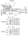
- Fig. 1A is a circuit diagram showing a conventional mode register control circuit 9 and a mode register 2 controlled by the mode register control circuit 9.
- a conventional mode register control circuit 9 may be built into an integrated SDRAM chip (semiconductor device) capable of high-speed outputting of data in response to an externally supplied high-speed clock.
- a semiconductor may be considered to comprise a mode register for storing operating mode data representing an operating mode of the semiconductor device; and mode register control circuitry operable, in response to an externally-applied mode register read command, to cause the stored operating mode data to be read out from the mode register and output by output circuitry of the device.
- the mode register control circuit 9 (indicated as MRGCTL in Fig. 1A) is provided in an SDRAM 1 so as to control operation of reading from the mode register 2 within tnhe SDRAM 1, in synchronism with an external command (mrspz) and external address data (a0 - a6, a8 and a9) fed via a terminal of the SDRAM 1.
- the mode register 2 latches an operating mode of the SDRAM 1 in response to a mode register set command and a mode register read command which are external commands.
- the mode register read command causes an operating mode of the SDRAM 1 chip to be output via an output terminal DQ provided on the SDRAM 1 chip.
- the mode register read command causes a mode selection signal (indicated as MRDZ in Fig. 1A) to be output via an output transistor 3 (indicated as outTr in Fig. 1A) connected to the output terminal DQ.
- a mode selection signal indicated as MRDZ in Fig. 1A
- an output transistor 3 indicated as outTr in Fig. 1A
- the mode register control circuit 9 is constructed to be capable of executing the mode register read command whether the mode register control circuit 9 is in an idle state or an active state. Since a normal reading operation is conducted after the chip becomes active, data is not output in an idle state.
- the mode register set command initiates an operating mode which controls the SDRAM 1 to be set to a desired operating mode by setting a CAS latency (CL) operating mode, a burst length (BL) operating mode and a burst type in the mode register 2.
- CL CAS latency
- BL burst length
- Setting of an operating mode (an operating mode initiated by the mode register set command, or an operating mode initiated by the mode register set command) in the mode register control signal 9 is effected by raising an operating mode signal (more specifically, CL1 - CL3 signals) selected when the mode register set command is executed. More specifically, as shown in Fig. 1A, address data a0 - a6, a8 and a9 input to the mode register 2 via an address input terminal ADD on the chip and specifying mode addresses are used to set the operating mode signal.
- the output transistor 3 (indicated as outTr in Fig. 1A) of the SDRAM 1 may be put in a low-impedance state when the mode register read command is input to the SDRAM 1 when the SDRAM 1 is turned on, or when it is determined that the mode register read command is latched in internal latching means in the SDRAM 1 (more specifically, an external command latching part or an external address latching part).
- the low-impedance state presents problems described later.
- the mode register read command allows data to be output when the SDRAM 1 is idle. Hence, if it is determined that the data is output via the output terminal DQ according to the mode register read command, mode data inside the mode register can be read from the output transistor of the SDRAM 1.
- predetermined data (a0 - a6, a8 and a9 shown in (b-2) of Fig. 1B) for selecting between the mode register set command and the mode register read command is input to the mode register 2 in synchronism with an internal clock of the SDRAM 1.
- the internal clock is a signal indicated as clkiz in (b-1) of Fig. 1B externally supplied via an external clock terminal CLK and an internal clock generating unit.
- a difference between the data setting for the mode register set command and that for the mode register read command is found only in a mode setting signal, that is, an a08 pin signal a8 supplied via the address input terminal ADD on the chip as address data specifying the mode address.
- the a8 signal is L, the mode register set command is specified; when H, the mode register read command is specified.
- the mode register control circuit 9 generates a register read signal (rgrz) (see (b-4) of Fig. 1B) which is a composite signal composed of the mode setting signal a8 and a mrspz signal (see (b-3) of Fig. 1B) which is generated in the external command latching part in the SDRAM 1 when the mode register set command or the mode register read command is latched, in synchronism with the external clock signal clkiz.
- rgrz register read signal
- the mode register control circuit 9 generates a driving signal mrrz (see (b-5) of Fig. 1B) which is the register read signal latched.
- the driving signal mrrz is latched until the next external clock clkiz is generated.
- the mode selection signal MRDZ stored in the mode register 2 is output (see (b-6) of Fig. 1B).
- the conventional mode register control circuit 9 if it is determined that data is output, when the SDRAM 1 is turned on, via the external output terminal DQ of the SDRAM 1 according to the mode register read command, or if it is determined that data is output in an idle state before the SDRAM 1 is turned on via the external output terminal DQ of the SDRAM 1 according to the mode register read command, the mode data inside the mode register is read from the output transistor of the SDRAM 1, causing the output transistor of the SDRAM 1 to be put in a low-impedance state. Therefore, the conventional mode register control circuit has a problem in that an abnormal current may flow when the SDRAM 1 is turned on or in an idle state occurring after the SDRAM 1 is turned on.
- a semiconductor device embodying the present invention is characterised in that the said mode register control circuitry comprises a control unit for preventing such reading out from the mode register in a power-up period in which the device begins to be supplied with power.
- the mode register control circuitry is capable of preventing an abnormal current from flowing in the SDRAM when the SDRAM is turned on or in an idle state occurring after the SDRAM is turned on, by providing such a control unit in the SDRAM (more specifically, in the mode register control circuit MRGCTL) for preventing the output transistor of the SDRAM from being in a low-impedance state even if it is determined that data is output, when the SDRAM is turned on, via an external output terminal of an SDRAM according to the mode register read command, or it is determined that data is output in an idle state before the SDRAM is turned on via the external output terminal DQ of the SDRAM according to the mode register read command.
- control unit uses internal means to disable, when the semiconductor device is turned on, execution of the mode register read command, using an initialising signal for specifying initialisation of a latch part for latching an external command and/or an external address externally fed to the semiconductor device, the initialisation being done during a transient state occurring after the semiconductor device is turned on.
- the mode register read command is enabled on the condition that the mode register set command is executed after the semiconductor device is turned on, so that an abnormal current is prevented from flowing in the output transistor of the semiconductor device. In an idle state occurring after the semiconductor device is turned on, an abnormal current is prevented from flowing in the output transistor of the semiconductor device.
- the mode register control circuitry may include an override circuit which, upon determining that an external command detected when the semiconductor device is turned on is other than a mode register read command, overrides the control unit so as to permit the mode register to execute a subsequent mode register read command even if a mode register set command has not ben executed after a power supply voltage becomes stable.
- an abnormal current is prevented from flowing in the output transistor of the semiconductor device, by disabling execution of the mode register read command when the semiconductor device is turned on.
- an abnormal current is prevented from flowing in the output transistor of the semiconductor device, by ensuring that execution of the mode register read command is enabled on the condition that the mode register set command is executed.
- the semiconductor device further comprises:
- a mode register control circuit 10 controls a semiconductor device 40 (SDRAM) capable of a data transfer speed higher than 100 Mbyte/sec.
- SDRAM semiconductor device 40
- Fig. 2 is a block diagram showing the mode register control circuit 10.
- An external clock signal clkiz is a signal input via an external clock terminal (CLK) 116 on the chip.
- An initializing signal sttz is a signal generated by a starter signal generating unit 101 on the chip so as to instruct latching circuits (specifically, an external command latching circuit 103 and an external address latching circuit 104) in the chip to be initialized when the SDRAM is turned on.
- a mrspz signal is generated by the external command latching circuit 103 in synchronization with the external clock signal clkiz, when the mode register set command or the mode register read command is fed via a command input terminal (CTL) 117 and latched in the external command latching circuit 103.
- a mode setting signal a8 is generated by the external address latching circuit 104 in correspondence with address data specifying mode address and input via the address input terminal (ADD) 118 on the chip.
- the external clock terminal (CLK) 116, the command input terminal (CTL) 117, the address input terminal (ADD) 118 and an output terminal (DQ) 119 are external terminals provided on the SDRAM 40 chip.
- the starter signal generating circuit 101 generates an initializing signal sttz for instructing latching circuits (more specifically, the external command latching circuit 103 and the external address latching circuit 104) to be initialized.
- the internal clock generating circuit 102 generates a clock signal for internal use in accordance with the external clock signal clkiz supplied via the external clock terminal (CLK) 116.
- the external address latching circuit 104 latches an external address signal (signal fed to the address input terminal (ADD) 118) in synchronism with the external clock signal clkiz supplied by the internal clock generating circuit 102.
- the external address signal is embodied by the address data a0 - a6, a9 and the mode setting signal a8.
- An external address decoding circuit 109 generates a mode type out of the external address signal.
- the external command latching circuit 103 latches an external command signal fed via the command input terminal (CTL) 117, that is, the mode register set command or the mode register read command, in synchronism with the external clock signal clkiz supplied from the internal clock generating circuit 102.
- CTL command input terminal
- An external command decoding circuit 110 generates internal commands such as a mode register set command out of an external command signal.
- the mode register control circuit 10 executes the mode register set command or the mode register read command in accordance with the external address signal (a0 - a6, a9), the mode setting signal (a8) and the mrspz signal.
- the mode register control circuit 10 generates a register set signal rgwz for instructing a mode register 20 to be set and also generates the register read signal rgrz for controlling the reading from the mode register.
- a register read control circuit 111 generates, in accordance with a register read signal rgrz, a driving signal mrrz for instructing the output transistor control circuit 120 to drive an output transistor (outTr) 30.
- the mode register 20 generates the mode selection signal (MRDZ) stored in the mode register 20, in accordance with the register read signal rgrz, the external address signal (a0 - a6, a9).
- the output transistor control circuit 120 controls the output transistor (outTr) 30 in accordance with the mode selection signal MRDZ.
- a memory cell array 113 is constructed such that memory cells each storing data in units of a bit are formed into layers in a predetermined manner.
- the memory cell array 113 stores write data from a write amplifier circuit 107.
- a sense amplifier 112 reads data stored in a memory cell of the memory cell array 113, temporarily stores the same, and transfers the same to a sense buffer 114.
- the sense amplifier 112 also temporarily stores the write data supplied by the write amplifier circuit 107 and stored in the sense buffer 114.
- the sense buffer 114 temporarily stores data read by the sense amplifier 112 or the write data transferred by the write amplifier circuit 107.
- a pipeline structure constructed of a pipeline 115 and a pipeline 108 one on top of the other executes a pipeline process for reading data stored in the sense buffer 114 in a parallel manner, in synchronism with an external clock signal clkiz.
- a write data latching circuit 105 temporarily stores data input via an external input terminal (DQ) 119B.
- the write amplifier circuit 107 writes the buffer latched in the write data latching circuit 105 in the sense buffer 114 in synchronism with the external clock signal clkiz.
- a write control circuit 106 controls the latching action of the write data latching circuit 105 and the write operation of the write amplifier circuit 107, in synchronism with the external clock signal clkiz.
- the SDRAM 40 is capable of outputting data at a data transfer speed of higher than 100 Mbyte/sec, in synchronism with a high-speed clock supplied via the external clock terminal 116.
- two operating modes are available: the mode register set mode and the mode register read mode.
- the mode register set command initiating the mode register set mode specifies the operating mode in which the SDRAM 40 is used.
- the mode register set command may set the CAS latency operating mode (CL), the burst length operating mode (BL) or the burst type in the mode register 2 in order to specify a specific operating mode.
- Setting of the operating mode is effected by raising the operating mode signal (specifically, CL1 - CL3 signals) selected when the mode register set command is executed. Specifically, as shown in Figs. 3A and 4A, predetermined data a0 - a6 and a9 is input to the mode register 20 so that the operating mode is set.
- the mode register read command causes an operating mode of the SDRAM 40 chip to be output via a terminal DQ (an output terminal 119A or the output terminal 119B) provided on the SDRAM 40 chip. More specifically, the mode register read mode is such that the mode selection signal (MRDZ shown in Figs. 3A and 4A) is output via the output transistor (outTr) 30 shown in Figs. 3A and 4A and connected to the terminal DQ (the output terminal 119A or the input terminal 119B).
- the mode selection signal MRDZ shown in Figs. 3A and 4A
- predetermined data (a0 - a6, a8 and a9) for selection between the mode register set command and the mode register read command is input to the mode register 20 in synchronism with the reception.
- a difference between the data setting for the mode register set command and that for the mode register read command is found only in a mode setting signal, that is, an a08 pin signal a8 supplied via the address input terminal (ADD) 118 on the chip as address data specifying the mode address.
- a8 signal is L, the mode register set command is specified; when H, the mode register read command is specified.
- the mode register control circuit 10 generates a register read signal rgrz which is a composite signal composed of the mode setting signal a8 and a mrspz signal which is generated in the external command latching circuit 103 in the SDRAM 40 when the mode register set command or the mode register read command is latched, in synchronism with the external clock signal clkiz.
- the mode register control circuit 10 generates a driving signal mrrz which is the register read signal rgrz latched.
- the driving signal mrrz is latched until the next external clock clkiz is generated.
- the mode selection signal MRDZ stored in the mode register 20 is output via the output transistor (outTr) 30.
- Fig. 3A is a circuit diagram showing a first embodiment of the present invention.
- Fig. 3B is a timing chart which explains an operation according to the first embodiment.
- the mode register control circuit (indicated as MRGCTL in Fig. 3A) 10 is provided in the SDRAM 40 so as to control operation of reading from the mode register within the SDRAM 40 in synchronism with the external command signal and the external clock signal.
- the mode register control circuit comprises a first control unit 202.
- the first control unit 202 disables, when the SDRAM 40 is turned on, execution of the mode register read command so as to prevent the content of the mode register from being read.
- the first control unit 202 uses an initializing signal sttz for instructing a transient state which occurs at power-on in the external command latching circuit 103 and the external address latching circuit 104 to be initialized, so that execution of the mode register read command is internally disabled.
- a starter signal sttz is used to set logical elements like flip-flop circuits constituting the external command latching circuit 103 and the external address latching circuit 104 at a predetermined potential level (more specifically, at logical H or logical L) so as to put the elements out of an unstable state occurring after the power is on.
- a prohibiting signal setz generated by the first control unit 202 is set to logical H (active) so as to prevent the mode register read command from being executed at the power-on. That is, no command for reading from the mode register 20 is output. In this way, the mode register read command is prevented by internal means from being executed when the SDRAM 40 is turned on, and the output transistor (output circuitry) 30 is prevented from being in a low-impedance state.
- the prohibiting signal setz generated by the first control unit 202 is set to logical (L) inactive when the mode register set command is executed after the SDRAM 40 is turned on, so as to enable reading from the mode register.
- a signal similar to (derived from the same source as) the register set signal rgwz output to set the mode register is used to reset the flip-flop circuits of the first control unit 202 which were initially set by the starter signal sttz. In this way, the prohibiting signal setz is maintained at logical L.
- the first control unit 202 enables execution of the mode register read command after execution of the mode register set command.
- phase (1) shown in Fig. 3B execution of the mode register read command is attempted. However, since the prohibiting signal setz generated by the first control unit 202 is at logical H, the register read signal rgrz generated by the mode register control circuit 10 is at logical L so that the output transistor 30 is maintained at a high-impedance state.
- phase (2) shown in Fig. 3B the mode setting signal a8 is set to logical L in order for the mode register set command to be executed. Subsequently, the mode register control circuit 10 outputs the register set signal rgwz so as to set the mode register 20. At the same time, the prohibition signal setz generated by the first control unit 202 is latched at logical L so that subsequent generation of the driving signal mrrz is enabled. Thus, subsequent execution of the mode register read command is enabled.
- phase (3) shown in Fig. 3B a bus that carries the register read signal rgrz generated by the mode register control circuit 10 is activated since the prohibition signal setz generated by the first control unit 202 is set at logical L as a result of the operation in phase (2).
- the mode setting signal a8 is set so that the mode register read command is executed.
- the mrspz signal in synchronism with the internal clock CLK is generated.
- the register read signal rgrz generated by the mode register control circuit 10 is output.
- the mode selection signal MRDZ which carries a content of the mode register 20 is output from the output transistor 30.
- phase (4) shown in Fig. 3B the output transistor 30 is reset by the internal clock CLK to a high-impedance state so that the whole operation is completed.
- the mode register control circuit 10 provided with the first control unit 202, execution of the mode register read command is prevented when the SDRAM 40 is turned on. In this way, an abnormal current is prevented from flowing in the output transistor 30 of the SDRAM 40.
- the SDRAM 40 comprises the mode register control circuit 10, the starter signal generating circuit 101 for generating an initializing signal sttz for instructing latching circuits to be initialized at power-on, the internal clock generating unit 102 for generating an internal clock clkiz in accordance with the external clock, the memory call array 113, a read/write circuit 130 responsible for reading data from the memory cell 113 and writing data into the same, an input/output circuit 140 responsible for inputting and outputting data addresses and commands, the mode register 20 storing the operating mode of the input/output circuit, and the register read control circuit 111 for controlling reading from the mode register in synchronism with the external clock.
- the read/write circuit 130 comprises the write data latching circuit 105, the write control circuit 106, the write amplifier circuit 107, the pipeline 108, the sense amplifier 112, the sense buffer 114, and the pipeline 115 which are described above.
- the input/output circuit 140 comprises the external command latching circuit 103, the external address latching circuit 104, the external address decoding circuit 109, the external command decoding circuit 110, and the output transistor control circuit 120.
- the SDRAM 40 provided with the mode register control circuit 10 it is possible to prevent an abnormal current from flowing in the output transistor (outTr) 30 by prohibiting execution of the mode register read command when the SDRAM 40 is turned on. In the idle state occurring after the SDRAM 40 is turned on, it is ensured that execution of the mode register read command is enabled on the condition that the mode register set command is executed so that an abnormal current is prevented from flowing in the output transistor (outTr) 30.
- Fig. 4A is a circuit diagram showing the second embodiment
- Figs. 4B and 4C are timing charts which explain the operation according to the second embodiment.
- the mode register control circuit 10 (indicated as MRGCTL in Fig. 4A) according to the second embodiment comprises a control unit (override circuit) 204 and a third control circuit (control unit) 206, as shown in Fig. 4A.
- the second control unit 204 Upon detecting that the external command detected when the SDRAM 40 is turned on is other than the mode register read command, the second control unit 204 enables the mode register to execute the mode register read command even if the mode register set command has not been executed after the power supply voltage is stabilized.
- the third control circuit 206 enables the mode register to execute the mode register read command when it is determined that the mode register set command is executed after the SDRAM 40 is turned on.
- the mode register control circuit 10 according to the second embodiment is provided with the second control unit 204 and the third control circuit 206, its added advantage over the mode register control circuit 10 according to the first embodiment is that under some circumstances operating mode type of the external command, latched in the mode register 20, can be read after power-up even if the mode register set command has not yet been executed.
- the mode register read command can be executed on the condition that an external command other than the mode register read command is executed after power-on. In this way, a normal internal operation can be effected.
- phase (1) shown in Fig. 4B the mrspz signal and the mrsqz signal in synchronism with the internal clock CLK, and the mode setting signal a8 are set to logical H, so that the second control unit (override circuit) 204 sets a set signal (responsive-setting signal) setR to logical L (inactive).
- the set signal setR set to logical L by the second control unit 204 is maintained at logical L after power-on.
- the third control circuit 206 latches the prohibiting signal setz to logical H (inactive), in response to the starter signal sttz and the set signal setR set to logical L by the second control unit 204.
- the output transistor 30 is prevented from being put in a low-impedance state at power-on and an abnormal current is prevented from flowing.
- phase (2) shown in Fig. 4B when the mode register set command is executed, the mode register control circuit 10 outputs the register set signal rgwz. At the same time as the mode register 20 is set, the prohibiting signal setz generated by the third control circuit 206 is latched at logical L so that subsequent generation of the driving signal mrrz is enabled. Thus, subsequent execution of the mode register read command is enabled.
- phase (3) shown in Fig. 4B the prohibiting signal setz is set by the third control circuit 206 at logical L as a result of the operation in phase (2). Therefore, the bus carrying the register read signal rgrz generated by the mode register control circuit 10 is activated. Further, the mode setting signal a8 is set to logical H to enable execution of the mode register read command, the mrspz signal in synchronism with the internal clock CLK is generated, and the register read signal rgrz is generated and output by the mode register control circuit 10. As a result, the mode selection signal MRDZ stored in the mode register 20 is output via the output transistor 30.
- phase (1) shown in Fig. 4C the mrspz signal or the mode setting signal a8 is set to logical L, so that the second control unit (override circuit) 204 sets the set signal (responsive-setting signal) setR to logical H (active).
- the set signal setR set to logical H by the second control unit 204 is maintained at logical H after power-on for the duration of phase (1).
- the third control circuit 206 latches the prohibiting signal setz to logical L.
- the output transistor 30 is prevented from being put in a low-impedance state.
- phase (2) shown in Fig. 4C the prohibiting signal setz generated by the third control circuit 206 remains latched at logical L so that in the second embodiment execution of the mode register read command is enabled and from this time onward the content of the register can be read after power-on even though no mode register setting command has yet been executed.
- execution of the mode register read command is disabled when the SDRAM 40 is turned on.
- the output transistor 340 By maintaining the output transistor 340 in a high-impedance state, an abnormal current is prevented from flowing into the output transistor 30 of the SDRAM 40.
- execution of the mode register read command is enabled by the third control circuit 206 subsequent to at least one execution fo the mode register set command.
- an abnormal current is prevented from flowing in the output transistor 30 of the SDRAM 40.
- the SDRAM 40 comprises the mode register control circuit 10, the starter signal generating circuit 101 for generating an initializing signal sttz for instructing latching circuits to be initialized at power-on, the internal clock generating unit 102 for generating an internal clock clkiz in accordance with the external clock, the memory cell array 113, the read/write circuit 130 responsible for reading data from the memory cell 113 and writing data into the same, the input/output circuit 140 responsible for inputting and outputting data addresses and commands, the mode register 20 storing the operating mode of the input/output circuit, and the register read control circuit 111 for controlling reading from the mode register in. synchronism with the external clock.
- the read/write circuit 130 comprises the write data latching circuit 105, the write control circuit 106, the write amplifier circuit 107, the pipeline 108, the sense amplifier 112, the sense buffer 114, and the pipeline 115 which are described above.
- the input/output circuit 140 comprises the external command latching circuit 103, the external address latching circuit 104, the external address decoding circuit 109, the external command decoding circuit 110, and the output transistor control circuit 120.
- the SDRAM 40 provided with the mode register control circuit 10 it is possible to prevent an abnormal current from flowing in the output transistor (outTr) 30 by prohibiting execution of the mode register read command when the SDRAM 40 is turned on. In the idle state occurring after the SDRAM 40 is turned on, it is ensured that execution of the mode register read command is enabled on the condition that the mode register set command is executed so that an abnormal current is prevented from flowing in the output transistor (outTr) 30.
- an abnormal current is prevented from flowing in the output transistor of the semiconductor device, by disabling execution of the mode register read command when the semiconductor device is turned on.
- an abnormal current is prevented from flowing in the output transistor of the semiconductor device, by ensuring that execution of the mode register read command is enabled on the condition that the mode register set command is executed.
Landscapes
- Dram (AREA)
Claims (11)
- Halbleitervorrichtung, enthaltend:dadurch gekennzeichnet, daß die Modusregistersteuerschaltung (10) eine Steuereinheit (202; 206) enthält, um das Auslesen aus dem Modusregister in der Einschaltperiode zu verhindern, in der die Leistungsversorgung der Vorrichtung beginnt.ein Modusregister (20) zum Speichern von Operationsmodusdaten (MRDZ), die einen Operationsmodus der Halbleitervorrichtung (40) darstellen; undeine Modusregistersteuerschaltung (10), die ansprechend auf einen extern angelegten Modusregisterlesebefehl so arbeitet, daß sie das Auslesen der gespeicherten Operationsmodusdaten aus dem Modusregister und das Ausgeben durch die Ausgangsschaltung (30) der Vorrichtung veranlaßt;
- Vorrichtung nach Anspruch 1, ferner enthaltend:wobei die Steuereinheit (202; 206) ferner so arbeitet, daß sie das Initialisierungssignal verwendet, um die Modusregistersteuerschaltung auf einen derartigen extern angelegten Modusregisterlesebefehl in der Einschaltperiode nicht ansprechend zu machen.Verriegelungsschaltungen (103, 104) zum Verriegeln eines Befehls und/oder einer Adresse, die extern an die Vorrichtung angelegt werden, welche Verriegelungsschaltungen in der Einschaltperiode durch ein Initialisierungssignal (sttz) initialisiert werden, das von einer Startsignalerzeugungsschaltung (101) der Vorrichtung erzeugt wird;
- Vorrichtung nach Anspruch 1 oder 2, bei welcher:die Modusregistersteuerschaltung (10) aus einem nicht ansprechenden Zustand, in dem diese Schaltung auf einen derartigen von außen angelegten Modusregisterlesebefehl nicht anspricht, in einen ansprechenden Zustand umschaltbar ist, in dem diese Schaltung auf einen derartigen von außen angelegten Modusregisterlesebefehl anspricht; unddie Steuereinheit (202; 206) so arbeitet, daß sie die Modusregistersteuerschaltung (10) in den nicht ansprechenden Zustand setzt, wenn die Vorrichtung am Beginn der Versorgung mit Leistung steht, und die Modusregistersteuerschaltung in den ansprechenden Zustand umschaltet, wenn ein extern angelegter Modusregistereinstellbefehl ausgeführt wird, nachdem die Vorrichtung mit Leistung versorgt wurde, welcher Modusregistereinstellbefehl dazu dient, diese Operationsmodusdaten in dem Modusregister (20) zu registrieren.
- Vorrichtung nach Anspruch 3, bei welcher:die Modusregistersteuerschaltung (10) ferner eine Lesesignalerzeugungsschaltung enthält, die einen Steuereingang hat, der mit der Steuereinheit (202; 206) verbunden ist, um von dieser ein Verbotssignal (setz) zu erhalten, und so arbeitet, daß sie dann, wenn das Verbotssignal inaktiv (L) ist, ein Registerlesesignal (rgrz) während der Ausführung eines derartigen Modusregisterlesebefehls erzeugt, um die Ausgangsschaltung (30) zu aktivieren, wobei die Erzeugung des Registerlesesignals (rgrz) gesperrt wird, wenn das Verbotssignal (setz) aktiv (H) ist; unddie Steuereinheit (202; 206) so arbeitet, daß sie das Verbotssignal (setz) aktiv (H) macht, wenn die Vorrichtung den nicht ansprechenden Zustand haben soll, und das Verbotssignal inaktiv (L) macht, wenn die Vorrichtung den ansprechenden Zustand haben soll.
- Vorrichtung nach Anspruch 4, bei welcher die Steuereinheit (202; 206) so angeschlossen ist, daß sie ein Rücksetzsignal erhält, das von der Modusregistersteuerschaltung (10) erzeugt wird, welches Rücksetzsignal von der gleichen Quelle wie das Registereinstellsignal (rgwz) erhalten wird, das an das Modusregister (20) während der Ausführung des Modusregistereinstellbefehls angelegt wird, wobei die Steuereinheit (202; 206) ansprechend auf das Rücksetzsignal so arbeitet, daß sie das Verbotssignal (setz) inaktiv (L) macht.
- Vorrichtung nach Anspruch 4 oder 5, angefügt an Anspruch 2 gelesen, bei welcher die Steuereinheit (202; 206) ansprechend auf das Initialisierungssignal (sstz) so arbeitet, daß sie das Verbotssignal (setz) aktiv (H) macht.
- Vorrichtung nach einem der Ansprüche 3 bis 6, bei welcher die Modusregistersteuerschaltung (10) ferner eine Übergehungsschaltung (204) enthält, die mit der Steuereinheit (206) verbunden ist, um zu verhindern, daß die Steuereinheit den nicht ansprechenden Zustand auswählt, wenn die Leistungsversorgung der Vorrichtung beginnt, vorausgesetzt, daß zu diesem Zeitpunkt kein Modusregisterlesebefehl an die Vorrichtung angelegt wird, wodurch die nachfolgende Ausführung eines Modusregisterlesebefehls nach dem Einschaltvorgang zugelassen wird, auch wenn kein derartiger Modusregistereinstellbefehl vorher ausgeführt wurde.
- Vorrichtung nach Anspruch 7, bei welcher die Übergehungsschaltung (204) so arbeitet, daß sie dann, wenn die Versorgung der Vorrichtung mit Leistung beginnt, erfasst, ob ein Modusregisterlesebefehl angelegt ist oder nicht, und dann, wenn dies der Fall ist, die Steuereinheit (206) veranlasst, den nicht ansprechenden Zustand auszuwählen, und dann, wenn dies nicht der Fall ist, die Steuereinheit (206) veranlasst, den ansprechenden Zustand auszuwählen.
- Vorrichtung nach Anspruch 8, bei welcher:die Steuereinheit (206) einen Steuereingang hat, der mit der Übergehungsschaltung (204) verbunden ist, um von dieser ein Ansprechend-Einstellsignal (setR) zu erhalten, und in dem Fall, daß das Ansprechend-Einstellsignal aktiv (H) ist, wenn die Versorgung der Vorrichtung mit Leistung beginnt, so arbeitet, daß sie den ansprechenden Zustand auswählt, und in dem Fall, in dem das Ansprechend-Einstellsignal inaktiv (L) ist, wenn die Versorgung der Vorrichtung mit Leistung beginnt, den nicht ansprechenden Zustand auswählt; unddie Übergehungsschaltung (204) so arbeitet, daß sie das Ansprechend-Einstellsignal (setR) aktiv (H) macht, wenn sie erfaßt, daß ein Modusregisterlesebefehl angelegt wurde, wenn die Versorgung der Vorrichtung mit Leistung beginnt und andernfalls das Ansprechend-Einstellsignal inaktiv (L) macht.
- Halbleitervorrichtung nach einem der vorstehenden Ansprüche, ferner enthaltend:eine interne Takterzeugungsschaltung (102) zum Erzeugen eines internen Taktsignals in Übereinstimmung mit einem externen Taktsignal;eine Speicherzellenanordnung (113);eine Lese-/Schreibschaltung (130) zum Lesen von Daten aus der und Schreiben von Daten in die Speicherzellenanordnung (113); undeine Eingabe-/Ausgabeschaltung (140) zum Eingeben und Ausgeben von Datenadressen und Befehlen.
- Vorrichtung nach einem der vorstehenden Ansprüche, bei welcher es sich um eine synchrone dynamische Speichervorrichtung mit wahlfreiem Zugriff (SDRAM) handelt.
Applications Claiming Priority (3)
| Application Number | Priority Date | Filing Date | Title |
|---|---|---|---|
| JP6353696 | 1996-03-19 | ||
| JP06353696A JP3351953B2 (ja) | 1996-03-19 | 1996-03-19 | モードレジスタ制御回路およびこれを有する半導体装置 |
| JP63536/96 | 1996-03-19 |
Publications (3)
| Publication Number | Publication Date |
|---|---|
| EP0797207A2 EP0797207A2 (de) | 1997-09-24 |
| EP0797207A3 EP0797207A3 (de) | 1997-11-26 |
| EP0797207B1 true EP0797207B1 (de) | 2002-05-29 |
Family
ID=13232043
Family Applications (1)
| Application Number | Title | Priority Date | Filing Date |
|---|---|---|---|
| EP96306782A Expired - Lifetime EP0797207B1 (de) | 1996-03-19 | 1996-09-18 | Halbleiteranordnung mit Modusregistersteuerschaltung |
Country Status (6)
| Country | Link |
|---|---|
| US (2) | US5699302A (de) |
| EP (1) | EP0797207B1 (de) |
| JP (1) | JP3351953B2 (de) |
| KR (1) | KR100208550B1 (de) |
| DE (1) | DE69621420T2 (de) |
| TW (1) | TW402803B (de) |
Cited By (1)
| Publication number | Priority date | Publication date | Assignee | Title |
|---|---|---|---|---|
| WO2006089313A3 (en) * | 2005-02-14 | 2007-01-18 | Qualcomm Inc | Register read for volatile memory |
Families Citing this family (30)
| Publication number | Priority date | Publication date | Assignee | Title |
|---|---|---|---|---|
| JPH1139894A (ja) * | 1997-07-23 | 1999-02-12 | Sharp Corp | クロック同期式読み出し専用メモリ |
| US6215725B1 (en) * | 1997-07-23 | 2001-04-10 | Sharp Kabushiki Kaisha | Clock-synchronized memory |
| JPH11134243A (ja) * | 1997-10-31 | 1999-05-21 | Brother Ind Ltd | 記憶装置の制御装置及びデータ処理システムにおける記憶装置の制御方法 |
| KR100257867B1 (ko) * | 1997-11-15 | 2000-06-01 | 윤종용 | 2차 캐시를 구비한 시스템 장치 및 동기형 메모리 장치 |
| JP3204384B2 (ja) * | 1997-12-10 | 2001-09-04 | エヌイーシーマイクロシステム株式会社 | 半導体記憶回路 |
| JP2000003589A (ja) * | 1998-06-12 | 2000-01-07 | Mitsubishi Electric Corp | 同期型半導体記憶装置 |
| DE19829287A1 (de) * | 1998-06-30 | 2000-01-05 | Siemens Ag | Dynamische Halbleiter-Speichervorrichtung und Verfahren zur Initialisierung einer dynamischen Halbleiter-Speichervorrichtung |
| JP2000036192A (ja) * | 1998-07-17 | 2000-02-02 | Fujitsu Ltd | 半導体集積回路 |
| KR100354873B1 (ko) * | 1999-12-28 | 2002-10-05 | 주식회사 하이닉스반도체 | 모드 레지스터 세팅 제어장치 |
| US6766447B1 (en) * | 2000-01-25 | 2004-07-20 | Dell Products L.P. | System and method of preventing speculative reading during memory initialization |
| US6901018B2 (en) * | 2001-07-18 | 2005-05-31 | Samsung Electronics Co, Ltd. | Method of generating initializing signal in semiconductor memory device |
| DE10232859B4 (de) * | 2001-07-18 | 2014-11-13 | Samsung Electronics Co., Ltd. | Verfahren zur Erzeugung eines Initialisierungssignals |
| US6687184B2 (en) * | 2001-08-28 | 2004-02-03 | Micron Technology, Inc. | Memory device having selectable clock input and method for operating same |
| US6721227B2 (en) * | 2002-02-11 | 2004-04-13 | Micron Technology, Inc. | User selectable banks for DRAM |
| FR2851668A1 (fr) * | 2003-02-24 | 2004-08-27 | St Microelectronics Sa | Procede et dispositif de selection de mode de fonctionnement d'un circuit integre |
| KR100516694B1 (ko) * | 2003-04-02 | 2005-09-22 | 주식회사 하이닉스반도체 | 반도체 메모리 장치 |
| KR100625293B1 (ko) * | 2004-06-30 | 2006-09-20 | 주식회사 하이닉스반도체 | 높은 신뢰성을 갖는 반도체메모리소자 및 그를 위한구동방법 |
| US8122187B2 (en) | 2004-07-02 | 2012-02-21 | Qualcomm Incorporated | Refreshing dynamic volatile memory |
| US7620783B2 (en) | 2005-02-14 | 2009-11-17 | Qualcomm Incorporated | Method and apparatus for obtaining memory status information cross-reference to related applications |
| US7640392B2 (en) | 2005-06-23 | 2009-12-29 | Qualcomm Incorporated | Non-DRAM indicator and method of accessing data not stored in DRAM array |
| KR100646941B1 (ko) * | 2005-07-25 | 2006-11-23 | 주식회사 하이닉스반도체 | 고주파수에서 안정적으로 파워 모드를 제어하기 위한반도체 메모리 장치 및 그것의 파워 모드 제어방법 |
| CN101401077A (zh) | 2006-03-31 | 2009-04-01 | 富士通株式会社 | 存储装置及其控制方法和其控制程序、存储卡、电路基板及电子设备 |
| WO2007116487A1 (ja) * | 2006-03-31 | 2007-10-18 | Fujitsu Limited | メモリ装置、そのエラー訂正の支援方法、その支援プログラム、メモリ・カード、回路基板及び電子機器 |
| JPWO2007116486A1 (ja) * | 2006-03-31 | 2009-08-20 | 富士通株式会社 | メモリ装置、その制御方法、その制御プログラム、メモリ・カード、回路基板及び電子機器 |
| US9262326B2 (en) | 2006-08-14 | 2016-02-16 | Qualcomm Incorporated | Method and apparatus to enable the cooperative signaling of a shared bus interrupt in a multi-rank memory subsystem |
| KR100955684B1 (ko) * | 2008-10-02 | 2010-05-06 | 주식회사 하이닉스반도체 | 플래그신호 생성회로 및 반도체 메모리 장치 |
| KR100961207B1 (ko) * | 2008-10-02 | 2010-06-09 | 주식회사 하이닉스반도체 | 커맨드 생성회로 및 반도체 메모리 장치 |
| JP2010182367A (ja) | 2009-02-05 | 2010-08-19 | Elpida Memory Inc | 半導体記憶装置 |
| KR101047000B1 (ko) | 2009-05-28 | 2011-07-06 | 주식회사 하이닉스반도체 | 모드레지스터리드 제어회로 및 이를 이용한 반도체 메모리 장치 |
| US9213491B2 (en) * | 2014-03-31 | 2015-12-15 | Intel Corporation | Disabling a command associated with a memory device |
Family Cites Families (6)
| Publication number | Priority date | Publication date | Assignee | Title |
|---|---|---|---|---|
| US5036495A (en) * | 1989-12-28 | 1991-07-30 | International Business Machines Corp. | Multiple mode-set for IC chip |
| JP3080520B2 (ja) * | 1993-09-21 | 2000-08-28 | 富士通株式会社 | シンクロナスdram |
| JPH07182864A (ja) * | 1993-12-21 | 1995-07-21 | Mitsubishi Electric Corp | 半導体記憶装置 |
| JP2697633B2 (ja) * | 1994-09-30 | 1998-01-14 | 日本電気株式会社 | 同期型半導体記憶装置 |
| US5598376A (en) * | 1994-12-23 | 1997-01-28 | Micron Technology, Inc. | Distributed write data drivers for burst access memories |
| US5526320A (en) * | 1994-12-23 | 1996-06-11 | Micron Technology Inc. | Burst EDO memory device |
-
1996
- 1996-03-19 JP JP06353696A patent/JP3351953B2/ja not_active Expired - Lifetime
- 1996-09-18 EP EP96306782A patent/EP0797207B1/de not_active Expired - Lifetime
- 1996-09-18 DE DE69621420T patent/DE69621420T2/de not_active Expired - Lifetime
- 1996-09-19 US US08/715,701 patent/US5699302A/en not_active Expired - Lifetime
- 1996-09-19 TW TW085111464A patent/TW402803B/zh not_active IP Right Cessation
- 1996-10-08 KR KR1019960044487A patent/KR100208550B1/ko not_active Expired - Lifetime
-
1997
- 1997-08-22 US US08/916,201 patent/US5812491A/en not_active Expired - Lifetime
Cited By (3)
| Publication number | Priority date | Publication date | Assignee | Title |
|---|---|---|---|---|
| WO2006089313A3 (en) * | 2005-02-14 | 2007-01-18 | Qualcomm Inc | Register read for volatile memory |
| KR100884448B1 (ko) * | 2005-02-14 | 2009-02-19 | 콸콤 인코포레이티드 | Dram 어레이에 저장되지 않은 sdram 모듈로부터의 데이터를 판독하기 위한 방법, 및 sdram 메모리 모듈 |
| EP2234114A1 (de) * | 2005-02-14 | 2010-09-29 | QUALCOMM Incorporated | Registerleseoperation eines flüchtigen Speichers |
Also Published As
| Publication number | Publication date |
|---|---|
| JP3351953B2 (ja) | 2002-12-03 |
| EP0797207A3 (de) | 1997-11-26 |
| JPH09259582A (ja) | 1997-10-03 |
| US5699302A (en) | 1997-12-16 |
| KR100208550B1 (ko) | 1999-07-15 |
| DE69621420T2 (de) | 2002-09-12 |
| TW402803B (en) | 2000-08-21 |
| US5812491A (en) | 1998-09-22 |
| EP0797207A2 (de) | 1997-09-24 |
| DE69621420D1 (de) | 2002-07-04 |
Similar Documents
| Publication | Publication Date | Title |
|---|---|---|
| EP0797207B1 (de) | Halbleiteranordnung mit Modusregistersteuerschaltung | |
| US6515928B2 (en) | Semiconductor memory device having a plurality of low power consumption modes | |
| US5379261A (en) | Method and circuit for improved timing and noise margin in a DRAM | |
| US20020159323A1 (en) | Semiconductor memory device | |
| US5663919A (en) | Memory device with regulated power supply control | |
| US11449086B2 (en) | Power voltage selection circuit | |
| JPH08180674A (ja) | ダイナミック・ランダム・アクセス・メモリ装置とその制御方法 | |
| JP2000100181A (ja) | フラッシュメモリ装置及びそのデ―タ読出し方法 | |
| US6396758B2 (en) | Semiconductor memory device | |
| US5305271A (en) | Circuit for controlling an output of a semiconductor memory | |
| US20030058724A1 (en) | Reduced current address selection circuit and method | |
| US5995436A (en) | Apparatus for controlling circuit response during power-up | |
| KR100419759B1 (ko) | 워드선 선택전에 사전부팅이 가능한 부팅회로를 구비한메모리장치 | |
| US6414879B1 (en) | Semiconductor memory device | |
| US6545919B1 (en) | Semiconductor memory and output signal control method and circuit in semiconductor memory | |
| KR100512546B1 (ko) | 제어 회로를 갖는 반도체 기억 장치 | |
| JPH08297965A (ja) | 半導体集積回路装置 | |
| JPH09198866A (ja) | 半導体記憶装置 | |
| JPH0973770A (ja) | 書き込みパルス発生回路 | |
| JPH08314886A (ja) | 半導体集積回路 | |
| KR19980077450A (ko) | 전원 전압의 레벨을 검출하기 위한 회로를 갖는 반도체 메모리 장치 | |
| KR20030079245A (ko) | 반도체 메모리 소자 | |
| HK1015521A (en) | Apparatus for controlling circuit response during power-up | |
| KR950030154A (ko) | 디램소자의 리프레쉬 방법 및 그 장치 | |
| KR19990047942A (ko) | 반도체 메모리 |
Legal Events
| Date | Code | Title | Description |
|---|---|---|---|
| PUAI | Public reference made under article 153(3) epc to a published international application that has entered the european phase |
Free format text: ORIGINAL CODE: 0009012 |
|
| AK | Designated contracting states |
Kind code of ref document: A2 Designated state(s): DE GB IT |
|
| PUAL | Search report despatched |
Free format text: ORIGINAL CODE: 0009013 |
|
| AK | Designated contracting states |
Kind code of ref document: A3 Designated state(s): DE GB IT |
|
| 17P | Request for examination filed |
Effective date: 19980203 |
|
| 17Q | First examination report despatched |
Effective date: 20000829 |
|
| GRAG | Despatch of communication of intention to grant |
Free format text: ORIGINAL CODE: EPIDOS AGRA |
|
| RTI1 | Title (correction) |
Free format text: SEMICONDUCTOR DEVICE COMPRISING MODE REGISTER CONTROL CIRCUIT |
|
| GRAG | Despatch of communication of intention to grant |
Free format text: ORIGINAL CODE: EPIDOS AGRA |
|
| GRAH | Despatch of communication of intention to grant a patent |
Free format text: ORIGINAL CODE: EPIDOS IGRA |
|
| GRAH | Despatch of communication of intention to grant a patent |
Free format text: ORIGINAL CODE: EPIDOS IGRA |
|
| GRAA | (expected) grant |
Free format text: ORIGINAL CODE: 0009210 |
|
| AK | Designated contracting states |
Kind code of ref document: B1 Designated state(s): DE GB IT |
|
| REG | Reference to a national code |
Ref country code: GB Ref legal event code: FG4D |
|
| REF | Corresponds to: |
Ref document number: 69621420 Country of ref document: DE Date of ref document: 20020704 |
|
| PLBE | No opposition filed within time limit |
Free format text: ORIGINAL CODE: 0009261 |
|
| STAA | Information on the status of an ep patent application or granted ep patent |
Free format text: STATUS: NO OPPOSITION FILED WITHIN TIME LIMIT |
|
| 26N | No opposition filed |
Effective date: 20030303 |
|
| REG | Reference to a national code |
Ref country code: GB Ref legal event code: 732E |
|
| PGFP | Annual fee paid to national office [announced via postgrant information from national office to epo] |
Ref country code: GB Payment date: 20090916 Year of fee payment: 14 |
|
| PGFP | Annual fee paid to national office [announced via postgrant information from national office to epo] |
Ref country code: IT Payment date: 20090916 Year of fee payment: 14 |
|
| GBPC | Gb: european patent ceased through non-payment of renewal fee |
Effective date: 20100918 |
|
| PG25 | Lapsed in a contracting state [announced via postgrant information from national office to epo] |
Ref country code: IT Free format text: LAPSE BECAUSE OF NON-PAYMENT OF DUE FEES Effective date: 20100918 |
|
| PG25 | Lapsed in a contracting state [announced via postgrant information from national office to epo] |
Ref country code: GB Free format text: LAPSE BECAUSE OF NON-PAYMENT OF DUE FEES Effective date: 20100918 |
|
| REG | Reference to a national code |
Ref country code: DE Ref legal event code: R082 Ref document number: 69621420 Country of ref document: DE Representative=s name: REICHERT & LINDNER PARTNERSCHAFT PATENTANWAELT, DE |
|
| REG | Reference to a national code |
Ref country code: DE Ref legal event code: R082 Ref document number: 69621420 Country of ref document: DE Representative=s name: REICHERT & LINDNER PARTNERSCHAFT PATENTANWAELT, DE Effective date: 20150512 Ref country code: DE Ref legal event code: R081 Ref document number: 69621420 Country of ref document: DE Owner name: SOCIONEXT INC., YOKOHAMA-SHI, JP Free format text: FORMER OWNER: FUJITSU SEMICONDUCTOR LTD., YOKOHAMA, KANAGAWA, JP Effective date: 20150512 |
|
| PGFP | Annual fee paid to national office [announced via postgrant information from national office to epo] |
Ref country code: DE Payment date: 20150916 Year of fee payment: 20 |
|
| REG | Reference to a national code |
Ref country code: DE Ref legal event code: R071 Ref document number: 69621420 Country of ref document: DE |