EP0796008B1 - Kamera mit digitaler und analoger Klemmschaltung - Google Patents
Kamera mit digitaler und analoger Klemmschaltung Download PDFInfo
- Publication number
- EP0796008B1 EP0796008B1 EP97104082A EP97104082A EP0796008B1 EP 0796008 B1 EP0796008 B1 EP 0796008B1 EP 97104082 A EP97104082 A EP 97104082A EP 97104082 A EP97104082 A EP 97104082A EP 0796008 B1 EP0796008 B1 EP 0796008B1
- Authority
- EP
- European Patent Office
- Prior art keywords
- circuit
- digital
- signal
- clamp
- analog
- Prior art date
- Legal status (The legal status is an assumption and is not a legal conclusion. Google has not performed a legal analysis and makes no representation as to the accuracy of the status listed.)
- Expired - Lifetime
Links
- 238000001444 catalytic combustion detection Methods 0.000 description 38
- 238000010586 diagram Methods 0.000 description 16
- 238000003384 imaging method Methods 0.000 description 16
- 230000015654 memory Effects 0.000 description 13
- 238000000034 method Methods 0.000 description 11
- 239000003086 colorant Substances 0.000 description 4
- 101001006776 Homo sapiens Kinesin-like protein KIFC1 Proteins 0.000 description 3
- 102100027942 Kinesin-like protein KIFC1 Human genes 0.000 description 3
- 238000006243 chemical reaction Methods 0.000 description 3
- 230000000875 corresponding effect Effects 0.000 description 3
- 230000000694 effects Effects 0.000 description 2
- 230000008707 rearrangement Effects 0.000 description 2
- 230000002411 adverse Effects 0.000 description 1
- 230000000052 comparative effect Effects 0.000 description 1
- 230000000295 complement effect Effects 0.000 description 1
- 238000007796 conventional method Methods 0.000 description 1
- 230000002596 correlated effect Effects 0.000 description 1
- 230000001419 dependent effect Effects 0.000 description 1
- 230000012447 hatching Effects 0.000 description 1
- 238000007689 inspection Methods 0.000 description 1
- 230000003287 optical effect Effects 0.000 description 1
- 230000002093 peripheral effect Effects 0.000 description 1
- 238000013139 quantization Methods 0.000 description 1
- 230000003252 repetitive effect Effects 0.000 description 1
- 238000005070 sampling Methods 0.000 description 1
- 238000000926 separation method Methods 0.000 description 1
- 238000010408 sweeping Methods 0.000 description 1
Images


Classifications
-
- H—ELECTRICITY
- H04—ELECTRIC COMMUNICATION TECHNIQUE
- H04N—PICTORIAL COMMUNICATION, e.g. TELEVISION
- H04N5/00—Details of television systems
- H04N5/14—Picture signal circuitry for video frequency region
- H04N5/16—Circuitry for reinsertion of DC and slowly varying components of signal; Circuitry for preservation of black or white level
- H04N5/18—Circuitry for reinsertion of DC and slowly varying components of signal; Circuitry for preservation of black or white level by means of "clamp" circuit operated by switching circuit
-
- H—ELECTRICITY
- H04—ELECTRIC COMMUNICATION TECHNIQUE
- H04N—PICTORIAL COMMUNICATION, e.g. TELEVISION
- H04N23/00—Cameras or camera modules comprising electronic image sensors; Control thereof
- H04N23/80—Camera processing pipelines; Components thereof
-
- H—ELECTRICITY
- H04—ELECTRIC COMMUNICATION TECHNIQUE
- H04N—PICTORIAL COMMUNICATION, e.g. TELEVISION
- H04N23/00—Cameras or camera modules comprising electronic image sensors; Control thereof
- H04N23/60—Control of cameras or camera modules
- H04N23/667—Camera operation mode switching, e.g. between still and video, sport and normal or high- and low-resolution modes
-
- H—ELECTRICITY
- H04—ELECTRIC COMMUNICATION TECHNIQUE
- H04N—PICTORIAL COMMUNICATION, e.g. TELEVISION
- H04N23/00—Cameras or camera modules comprising electronic image sensors; Control thereof
- H04N23/80—Camera processing pipelines; Components thereof
- H04N23/84—Camera processing pipelines; Components thereof for processing colour signals
- H04N23/843—Demosaicing, e.g. interpolating colour pixel values
-
- H—ELECTRICITY
- H04—ELECTRIC COMMUNICATION TECHNIQUE
- H04N—PICTORIAL COMMUNICATION, e.g. TELEVISION
- H04N25/00—Circuitry of solid-state image sensors [SSIS]; Control thereof
- H04N25/10—Circuitry of solid-state image sensors [SSIS]; Control thereof for transforming different wavelengths into image signals
- H04N25/11—Arrangement of colour filter arrays [CFA]; Filter mosaics
- H04N25/13—Arrangement of colour filter arrays [CFA]; Filter mosaics characterised by the spectral characteristics of the filter elements
- H04N25/134—Arrangement of colour filter arrays [CFA]; Filter mosaics characterised by the spectral characteristics of the filter elements based on three different wavelength filter elements
-
- H—ELECTRICITY
- H04—ELECTRIC COMMUNICATION TECHNIQUE
- H04N—PICTORIAL COMMUNICATION, e.g. TELEVISION
- H04N25/00—Circuitry of solid-state image sensors [SSIS]; Control thereof
- H04N25/40—Extracting pixel data from image sensors by controlling scanning circuits, e.g. by modifying the number of pixels sampled or to be sampled
- H04N25/44—Extracting pixel data from image sensors by controlling scanning circuits, e.g. by modifying the number of pixels sampled or to be sampled by partially reading an SSIS array
- H04N25/447—Extracting pixel data from image sensors by controlling scanning circuits, e.g. by modifying the number of pixels sampled or to be sampled by partially reading an SSIS array by preserving the colour pattern with or without loss of information
-
- H—ELECTRICITY
- H04—ELECTRIC COMMUNICATION TECHNIQUE
- H04N—PICTORIAL COMMUNICATION, e.g. TELEVISION
- H04N5/00—Details of television systems
- H04N5/222—Studio circuitry; Studio devices; Studio equipment
- H04N5/262—Studio circuits, e.g. for mixing, switching-over, change of character of image, other special effects ; Cameras specially adapted for the electronic generation of special effects
- H04N5/2628—Alteration of picture size, shape, position or orientation, e.g. zooming, rotation, rolling, perspective, translation
-
- H—ELECTRICITY
- H04—ELECTRIC COMMUNICATION TECHNIQUE
- H04N—PICTORIAL COMMUNICATION, e.g. TELEVISION
- H04N2209/00—Details of colour television systems
- H04N2209/04—Picture signal generators
- H04N2209/041—Picture signal generators using solid-state devices
- H04N2209/042—Picture signal generators using solid-state devices having a single pick-up sensor
- H04N2209/045—Picture signal generators using solid-state devices having a single pick-up sensor using mosaic colour filter
- H04N2209/046—Colour interpolation to calculate the missing colour values
-
- H—ELECTRICITY
- H04—ELECTRIC COMMUNICATION TECHNIQUE
- H04N—PICTORIAL COMMUNICATION, e.g. TELEVISION
- H04N25/00—Circuitry of solid-state image sensors [SSIS]; Control thereof
- H04N25/10—Circuitry of solid-state image sensors [SSIS]; Control thereof for transforming different wavelengths into image signals
- H04N25/11—Arrangement of colour filter arrays [CFA]; Filter mosaics
- H04N25/13—Arrangement of colour filter arrays [CFA]; Filter mosaics characterised by the spectral characteristics of the filter elements
- H04N25/135—Arrangement of colour filter arrays [CFA]; Filter mosaics characterised by the spectral characteristics of the filter elements based on four or more different wavelength filter elements
- H04N25/136—Arrangement of colour filter arrays [CFA]; Filter mosaics characterised by the spectral characteristics of the filter elements based on four or more different wavelength filter elements using complementary colours
Definitions
- the present invention relates to digital cameras, and more particularly to a digital camera adapted to process analogically and digitally an image signal from a CCD using a mosaic-type color filter or a stripe-type color filter, for example, so as to clamp a black level.
- a principle object of the invention is to provide a digital camera capable of clamping a digital signal in an appropriate manner.
- the above object is achieved by a digital camera according to claim 1.
- the dependent claims are related to further advantages aspects of the present invention.
- a digital camera comprises an imager for outputting line signals, each of the line signals being clamped in an analog clamp area of the imager by an analog clamp means and then converted into a digital signal, the digital signal being digital-clamped in a digital clamp area by a digital clamp means, the digital video camera characterized in that: the analog clamp area is set such that both horizontal ends of the analog clamp area are positioned at the outside of the digital clamp area.
- the analog clamp means clamps each line signal outputted from the imager in the analog clamp area, while the digital clamp means clamps the digital signal in the digital clamp area.
- the analog clamp area is set such that the both horizontal ends thereof are positioned at the outside of the digital clamp area. That is, the analog clamp area is set such that it covers the digital clamp area at least with respect to a horizontal direction, or set at a different area from the digital clamp area.
- the both horizontal ends of the analog clamp area are arranged so as to be positioned at the outside of the digital clamp area, so that it is possible to appropriately clamp the output.
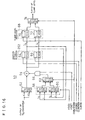
- a digital video camera 10 of a first embodiment shown in Figure 1 includes a solid-state imaging device unit or CCD imager 12, and this solid-state imaging device unit 12 includes as shown in Figure 3 the number of M of photodiodes 14 for photoelectric conversion and vertical transfer CCDs 16.
- the vertical transfer CCDs 16 are driven by a vertical driving circuit 18, while a horizontal transfer CCDs 20a and 20b are driven by a horizontal driving circuit 22.
- the horizontal transfer CCDs 20a and 20b are arranged in parallel therewith a drain 24, which drain 24 is utilized for sweeping off unwanted electric charges during high-speed photographing. That is, the electric charges, which have delivered through sweep-off control gates 26 from the horizontal transfer CCDs 20a and 20b, are swept off out of the drain 24.
- the solid-state imaging device unit or CCD imager 12 is attached with a primary-color filter shown in Figure 2, so that signals of the same number of lines as the number of pixels in a vertical direction, i.e. 480 are read out of the horizontal transfer CCDs 20a and 20b. That is, this solid-state imaging device unit 12 is of dual-channel structure that is intended to improve on a resolution by once reading out data of all pixels in one field, without mixing electric charges between vertical two pixels.
- the solid-state imaging unit or CCD imager 12 operates in accordance with a field storage mode shown in Figure 4. That is, the electric charges stored on photodiodes 14 are read once per one field to the vertical transfer CCDs 16. Thereafter, two vertical transfer pulses are successively supplied to the vertical transfer CCDs 16, and electric charges of two lines are simultaneously transferred once per 1H respectively to the horizontal transfer CCDs 20a and 20b.
- the horizontal transfer CCDs 20a and 20b each output electric charges of one line per 1H depending upon a horizontal transfer clock.
- the horizontal CCDs 20a outputs an output of an odd line, 1, 3, 5 ..., as a first channel output therefrom, while the horizontal CCDs 20b outputs an output of an even line, 2, 4, 6 ..., as a second channel output therefrom.
- This enables outputting, from the solid-state imaging device unit 12, of electric charges for all the pixels included in an effective pixel area and a shield area shown in Figure 12.
- an electric-charge read-out pulse in this mode is supplied once per 1/4 field to the vertical transfer CCDs 16 as shown in Figure 6. Further the vertical transfer CCDs 16 are driven by vertical transfer pulses outputted 2 in number every 1/2H and in number of 240 during a horizontal blanking period every 1/4 field. Accordingly, the electric charges of two lines are transferred every 1/2H to the horizontal transfer CCDs 20a and 20b.
- a sweep-off pulse is supplied to thereby open the sweep-off control gate 26. Accordingly, the electric charges for the latter half of the one line are swept off from the drain 26 through the sweep-off control gate 26. That is, in the quadruple-speed photographing mode, the electric charges only for the first half on each line are outputted from the horizontal transfer CCDs 20a and 20b, while the electric charges for the latter half on each line are swept off from the drain 24. Specifically, the first half signals on odd lines 1 to 239 are outputted from the horizontal transfer CCD 20a, and the first half signals on even lines 2 to 240 are outputted from the horizontal transfer CCD 20b. Incidentally, the electric charges for pixels involved in the first four lines, amongst the electric charges outputted out of the vertical transfer CCDs 16, are the electric charges being in the shield area.
- one screen is constituted by eight images which are horizontally compressed to 1/2 in image at the upper left 1/4 portion of the CCD screen.
- the images on the left and right are images to be respectively formed by the odd line and the even line on the same time base.
- the solid-state imaging device unit 12 operates on the ordinary photographing mode when the quadruple-speed switch 28 is not manipulated, and operates on the quadruple-speed mode when the quadruple-speed switch 28 is manipulated.
- the camera signal from the solid-state imaging device unit or CCD imager 12 is delivered by each channel to the signal processing circuits 30a and 30b where it is subjected to processing such as AGC, analog clamping, A/D conversion, digital clamping, etc. Therefore, color camera signals are outputted from the signal processing circuits 30a and 30b.
- the color camera signal from the signal processing circuit 30a is delivered as it is to a contact 32a of a switch 132, and to a contact 132b of the switch 132 through a rearrangement circuit 34a.
- the color camera signal from the signal processing circuit 30b is delivered as it is to a contact 232a of a switch 232, and to a contact 232b of a switch 232 through a reordering circuit 34b.
- the switches 132 and 232 are in interlocking to a quadruple-speed switch 28, so that they are connected to the contacts 132a and 232a when the quadruple-speed switch 28 is off and connected to the contacts 132b and 232b when the quadruple-speed switch 28 is on.
- the reordering circuit 34a includes eight memories a1, a2, b1, b2, c1, c2, d1, and d2, and a memory control circuit 36.
- the respective memories a1, a2, b1, b2, c1, c2, d1, and d2 are a memory for 1/8 screen to store signals for eight regions A1, A2, B1, B2, C1, C2, D1 and D2 shown in Figure 5.
- the memories a1 and a2 are alternately written with signals every 1/2H for a first 1/4 field, and the memories b1 and b2 are alternately written with signals every 1/2H for a next 1/4 field. In this manner, all the memories a1, a2, b1, b2, c1, c2, d1 and d2 are written with color camera signals.
- the memories a1, b1, a2 and b2 are repeatedly read out in order responsive to a read enable signal for a first 1/2 field period (first half field), and the memories c1, d1, c2 and d2 are repeatedly read out in order for a next 1/2 field period (latter half field).
- the reordering circuit 34b is similarly configured to the reordering circuit 34a, and duplicated descriptions will be omitted.
- the color camera signals shown in Figure 5(C) are outputted from the reordering circuit 34a and 34b.
- the color camera signal outputted from the switches 132 and 232 is inputted to an interpolation processing circuit 100.
- the interpolation processing circuit 100 is configured as in Figure 10. That is, a first channel output inputted through the switch 132 is supplied directly or through a 1H delay circuit 116 respectively as D0 and D2 to a selecting circuit 118, and a second channel output inputted through the switch 232 is supplied directly or through a 1H delay circuit 117 respectively as D1 and D3 to the selecting circuit 118.
- the 1H delay circuits 116 and 117 are memories which can store an inputted CCD output for a 1H time period, with a result that a CCD output with 1H delay is obtained by passing a signal through the same circuit. Incidentally, write-in or read-out of a signals to the 1H delay circuit is executed in synchronism with the horizontal transfer in the horizontal transfer CCD.
- the selecting circuit 118 selects digital signals of 3 lines out of digital signals of adjacent 4 lines depending upon whether a field under processing is of an odd field or an even field. For the odd field, D0 to D3 are respectively outputted as L0 to L2, whereas for the odd field D0 to D2 are respectively outputted as L0 to 2.
- the outputs L0 to L2 of the selecting circuit 118 are inputted directly to an interpolation calculating circuit 133 and to a delay circuit 130. Further, the outputs of the delay circuit 130 are inputted to a delay circuit 131.
- both the delay circuits 130 and 131 have a delay time for one pixel, and the outputs of the delay circuits 130 and 131 are inputted to the interpolation calculating circuit 133.
- the interpolation calculating circuit 133 is inputted with signals for successive 3 pixels of adjacent 3 lines, i.e. signals for 9 pixels are simultaneously inputted to the interpolation calculating circuit 133.
- the color filter in this embodiment has filters of three primary colors arranged in a mosaic form wherein either only one of R, G and B can be obtained from any of pixels, the signals for the other two colors are interpolated with the surrounding pixels by the interpolation calculating circuit 133.
- the relations between the arrangement of pixels on the solid-state imaging unit 12 and pixels to be selected are represented as in Figure 11.
- the line signals D1 to D3 are selected so that a pixel pattern at an odd number is represented as Figure 11(b).
- a pixel pattern at an even number becomes as shown in Figure 11(c).
- Figure 11(d) demonstrates a typical arrangement of part of pixels on the solid-state imaging unit 12.
- the interpolation calculating circuit 132 obtains a G signal from the central pixel and outputs the G signal as it is, obtains R signals from upper and lower pixels in the centered vertical column and taking an average on these two pixel signals to output as R signals, and obtains B signals from the left and right two pixels in the centered horizontal line and taking an average on these two pixel signals to output as B signals. Also, in the case of (c), R and G signals are available by taking average on the same color signals for adjacent four pixels.
- the signals for the pixels under process lacking two colors are prepared and interpolated by the peripheral same-colored pixel signal, thereby outputting R, G, and B signals for pixels.
- the color camera signal outputted from the interpolation calculating circuit 132 is delivered to a recording circuit (not shown), as well as to a contact 38a of a switch 38 and to a contact 38b of the switch 38 by way of a zooming-up circuit 40.
- the magnifying circuit 40 in the quadruple-speed photographing mode, magnifies twice the color camera signal from the switch 32 in respective horizontal and vertical directions.
- the switch 38 interlocks to the quadruple-speed switch 28, similarly to the aforesaid switch 32.
- the quadruple-speed switch 28 when the quadruple-speed switch 28 is off, the color camera signal from the switch 32 is delivered as it is to a viewfinder (not shown), while, when the quadruple switch 28 is on, the viewfinder is delivered with a color camera signal magnified by the magnifying circuit 40 to be outputted from the switch 38.
- the ordinary photographing mode i.e. the first photographing mode
- the quadruple-speed photographing mode i.e. the second photographing mode
- a clamping process in the signal processing circuit 30a will be explained hereinbelow. Incidentally, the clamping process in the signal processing circuit 30a also similar to the signal processing circuit 30b, and duplicated explanations will be omitted.
- the signal processing circuit 30a shown in Figure 12 of this embodiment includes an automatic gain control (AGC) circuit 42 for receiving an output signal, which has been removed of reset noise by a correlated double sampling circuit (not shown), from the solid-state imaging device unit or CCD imager 12.
- AGC automatic gain control
- This AGC circuit 42 processes an output signal from the solid-state imaging device unit 12 to an optimal amplitude in dependence upon an AGC voltage from the AGC-voltage generating circuit (not shown) for generation of an AGC voltage based on a gain control signal delivered as for example a PWM signal from a CPU 44.
- the output signal adjusted in amplitude by the AGC circuit 42 is clamped by the analog clamp circuit 43. More specifically, a switch 43a included in the analog clamp circuit 43 is turned on corresponding to, in a shield area shown in Figure 13, a first analog clamp area set at a rear edge of each line or a second analog clamp area set at a lower edge to an effective pixel area. That is, in the ordinary-speed photographing mode the switch 43a is turned on by gate signals of a vertical pulse V1 and a horizontal pulse H1 corresponding to the first analog clamp area, whereas in the quadruple-speed photographing the switch 43a is turned on by gate pulses of a vertical pulse V1 and a horizontal pulse H2 corresponding to the second analog clamp area.
- This causes the output signal of the AGC circuit 42 to be clamped at a reference voltage V2, and the clamped signal is inputted to an A/D converter 46 through a buffer amplifier 43a.
- the A/D converter 43 is given of a reference voltage V1 by which a minimal value level of the A/D converter is prescribed. Consequently, the A/D converter 46 quantizes an input signal with the reference voltage V2 as reference, creating a digital signal.
- the reference voltages V1 and V2 are obtained by voltage-dividing a power supply voltage Vcc with resistances R1 to R3, resulting in the reference voltage V1 > V2.
- the digital signal is adjusted in black level by clamping the output signal from the AGC circuit 42 by the reference voltage V2 and quantize it with the reference voltage V1 as a minimum value.
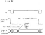
- the adjustment like this is due to the following reason. That is, although the digital signal from the A/D converter 46 is clamped at a level shown in Figure 21(A) and Figure 22(A), if the black level of the digital signal outputted from the A/D converter 46 rises excessively high or falls excessively low, there occurs saturation in white level for the digital signal or saturation in part of random-noise components superimposed by the black level, with the result that the dynamic range is reduced small or "black floating" becomes impossible to be prevented.
- first analog clamp area and the second analog clamp area are set such that their respective horizontal ends are respectively positioned at first and second clamp areas so that analog clamping will not have adverse effects on digital clamping. That is, in the ordinary-speed photographing mode, the turning on/off of the switch 43a at both horizontal ends of the first analog clamp area causes superposition of noise on the output signal from the AGC circuit 42, as shown in Figure 15. However, as will be understood from Figure 13 and Figure 14, since the first analog clamp area is set broader than the first digital clamp area, there is no possibility that this noise badly influences upon the later processes. Also, in the quadruple-speed photographing mode, a second analog clamp area and a second digital clamp area are set such that they are not overlapped with so that, in also this mode, the noise caused during analog clamping will not badly affect the digital clamping.
- the digital signal is delivered to an adding circuit 48 and a clamp-level calculating circuit 50.
- an offset value given from an CPU 44 is added to the digital signal outputted from the A/D converter 46.
- the offset value is preferably set in accordance with the magnitude of a gain to be set in the AGC circuit 42. For example, where the gain of the AGC circuit 42 is great the offset value is rendered large, and where reverse the offset value is rendered small.
- the clamp-level calculating circuit 50 calculates an average value (referred to as "OB level") of an optical black (OB) portion of each line in a first digital clamp area set at a rear edge of each line or a second digital clamp area set at a front edge of each line, in a shading area shown in Figure 14, to calculates a clamp level based thereon.
- OB level an average value of an optical black (OB) portion of each line in a first digital clamp area set at a rear edge of each line or a second digital clamp area set at a front edge of each line, in a shading area shown in Figure 14, to calculates a clamp level based thereon.
- the clamp level calculating circuit 50 is shown in Figure 16.
- the clamp level calculating circuit 50 includes a selecting circuit 52 for receiving a digital signal (input data) of for example 8 bits from the A/D converter 46.
- This selecting circuit 52 selectively outputs one times the input data ((1) or two times thereof ((2) to deliver it to an adding circuit 54.
- the adding circuit 54 is delivered with data selected by a selecting circuits 58, 60 through an AND gate 56.
- the AND gate 56 is controlled by a signal VSET shown in Figure 17 and Figure 18.
- the signal VSET is a signal that becomes a low level only at respective odd and even one pixels at which the first digital clamp area and the second digital clamp area begins.
- the selecting circuits 58 and 60 are controlled by a signal HSET shown in Figure 17 and Figure 18, to selectively output 1/2 times (1/2) or one times (1) a data delivered.
- This signal HSET as shown in Figure 17 or Figure 18, is a signal that becomes a low level at odd-and-even two pixels at a beginning end for the first digital clamp area or the second digital clamp area on each line.
- the selecting circuit 62 is controlled by a signal ODD/EVEN, which selects to output an output of the selecting circuit 58 when the signal ODD/EVEN is at a high level, and an output of the selecting circuit 60 when at a low level.
- This signal ODD/EVEN goes to a high level for an odd pixel of the CCD and to a low level for an even pixel.
- the output of the adding circuit 54 is delivered to an adding register 262.
- This adding register 262 includes an odd register 64 and an even register 66, so that an odd pixel data of the output of the adding circuit 54 is delivered to the odd register 64 and an even pixel data is delivered to the even register 66.
- the outputs from the odd register 64 and the even register 66 are respectively delivered to the aforesaid two selecting circuits 58 and 60, as well as to an odd register 70 and an even register 72 included by a clamp-value register 68.
- the adding register 262 latches the output from the adding circuit 54, while the clamp-value register 68 latches the output from the adding register 262. Note that the outputs from the odd register 64 and the even register 66 of the adding register 262 are respectively rendered 1/16 to be latched to the odd register 70 and the even register 72 of the clamp-value register 68.
- the odd register 64 of the adding register 262 receives a signal CLKODD as a latch signal
- the even register 66 receives CLKEVEN as a latch signal.
- the signal CLKODD is a clock that is outputted on every odd pixel
- the signal CLKEVEN a clock outputted on every even pixel.
- the odd register 70 and the even register 72 of the clamp-value register 68 are delivered with a signal CLKHD as a common latch timing signal.
- the signal CLKHD is a signal that goes to a high level only at one pixel at the right end of each line shown in Figure 14.
- the outputs of the odd register 70 and the even register 72 of the clamp-value register 68 are delivered to a selecting circuit 74.
- the selecting circuit 74 is controlled by the signal ODD/EVEN similarly to the aforesaid selective circuit 62, and select to output an output of the odd register 70 when the signal ODD/EVEN is at the high level and an output of the even register 72 when at the low level.
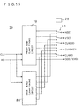
- timing generator 76 shown in Fig 1. That is, the timing generator 76 includes as part thereof a front-edge clamp timing circuit 78 and a rear-edge clamp timing circuit 80 sown in Figure 19.
- the front-edge clamp timing circuit 78 and the rear-edge clamp timing circuit 80 both receive a master clock CLK and a horizontal synchronizing signal HD to prescribe a second digital clamp area (second predetermined time period) and a first digital clamp area (first predetermined time period).
- the front-edge clamp timing circuit 78 is configured by an appropriate gate circuit and a ROM decoder, to output a timing signal shown in Figure 18 only for a time (second predetermined time period) for odd two pixels and even two pixels of each line signal in the second digital clamp area, based on the master clock CLK and the horizontal synchronizing signal HD.
- the rear-edge clamp timing circuit 80 is similarly configured by an appropriate gate circuit and a ROM decoder, to output a timing signal shown in Figure 17 only for a time by odd two pixels and even eight pixels of each line signal in the first digital clamp area, based on the master clock CLK and the horizontal synchronizing signal HD.
- the output signals of the front-edge timing circuit 78 and the rear-edge timing circuit 80 are switched over by a switch 81 interlocking to the quadruple-speed switch 28 for being outputted. Consequently, the clamp level calculating circuit 50 operates responsive to the timing signals outputted from the front-edge clamp timing circuit 78 or the rear-edge clamp timing circuit 80 of the timing generator 76.
- an OB level of 8 pixels is calculated as to odd pixels.
- the selecting circuit 52 is selected at "(2" at timing of a line to be clamped. Accordingly, the input data is shifted up by one bit with the result that a data two times the input is outputted from the selecting circuit 52.
- the signal VSET as an control input to the AND gate 56 becomes a low level as shown in Figure 17 so that the output of the adding circuit 54 is of a data two times a first odd pixel data outputted from the selecting circuit 52.
- This two-times data is inputted to each of registers 64 and 66 of the adding register 262, to be latched to the odd register 64 depending on a signal CLKODD shown in Figure 17.
- This data latched to the odd register 64 is delivered to the selecting circuit 58.
- the selecting circuit 58 outputs to the selecting circuit 62 the data one-time multiplied of the input data in accordance with the low level of the signal HSET.
- the selecting circuit 62 selects an upper side input when the signal ODD/EVEN is at a high level, and selects an lower side input when it is at a low level, with the result that the one-times of odd pixel data from the selecting circuit 58 is delivered from the selecting circuit 62 to the AND gate 56. That is, the data inputted to the AND gate 56 is a data two times the first odd pixel.
- a selecting circuit 74 outputs an OB level data of odd 8 pixels of a first line in the first digital clamp area ( Figure 14) latched to the odd register 70 responsive to the high level of the ODD/EVEN signal.
- the subsequent lines that is a second line and the subsequent, the selecting circuit 52 selects "(1", and the selecting circuits 58 and 60 select "1/2" only for the first one pixel and "1" for the subsequent 7 pixels. Accordingly, a 16-times data is outputted from the adding register 62 and rendered "1/16", resulting in outputting of an OB level of 8 pixels on each line from the selecting circuit 74. That is, a recursive filter is configured by a circuit passing from the adding circuit 54 through the adding register 262, the selecting circuits 58, 60 and 62, and the AND gate 56.
- the weighting coefficient (k) of the recursive filter is set at "1/2"
- this coefficient can be set arbitrary within a range of 0 ⁇ k ⁇ 1. That is, by setting the coefficient (k) the clamp level of the first line remains in the OB level value as it is, and the clamp level for the line 2 and the subsequent becomes a weighted mean of coefficient (k) for the clamp level of the previous line and a newly obtained OB level. Therefore, even if there is noise contained in the OB portion of the line 2 and the subsequent, the influence thereof is relieved to 1/k times.
- the operation of the clamp level calculating circuit 50 for the second predetermined period is similar to the operation of the first predetermined period, and duplicated explanations will be omitted. Note that the OB level of two pixels is calculated for the second predetermined period.
- the clamp level is outputted from the clamp level calculating circuit 50 to be inputted to a first subtraction circuit 82 shown in Figure 12. Accordingly, the first subtracting circuit 82 subtracts the clamp level calculated by the clamp level calculating circuit 50 from the data added with the offset value by the adding circuit 50, and the digital signal from the A/D converter 46 is digitally clamped.
- the output of the first subtraction circuit 82 is zero-clipped (a negative numeral value is forced to a zero-level) zero-clip circuit 84 including for example such as an OR gate, and then delivered through a digital low-pass filter 86 to a second subtraction circuit 88.
- the subtraction input to the second subtraction circuit 88 is given of the same offset value as that delivered from the CPU 44 to the adding circuit 48.
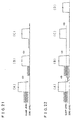
- Figure 21(A) and Figure 22(A) each shows a CCD output signal (digital signal) for one line outputted from the A/D converter 46 where photographing a subject in black on the left and white on the right.
- the actual signal assumes a waveform as shown in Figure 21(A) or Figure 22(A) because it contains random noises.
- the clamp level is at a level denoted by the dotted line, at which level clamping is done by the first subtraction circuit 82.
- the output of the zero-clip circuit 84 is a signal as in Figure 21(B).
- This signal if passes through the low-pass filter 80, has a waveform as in Figure 21(C), wherein a portion of the signal to be in black is not zero and hence there occurs a phenomenon called "black floating".
- the output signal of the zero-clip circuit 84 has a waveform shown in Figure 22(B). If this is processed by the low-pass filter 80, the waveform becomes as shown in Figure 22(C). Thereafter, by subtracting the offset value by the second subtraction circuit 88, the optically-black portion in the signal becomes nearly zero, providing an image signal free from "black floating".
- the offset value is varied in accord with the gain by the AC circuit 42. That is, when the gain is large, noise is also large, so that the offset value is taken great to prevent against black floating. When the gain is small, the noise also small, and accordingly the offset value is taken small to broaden the dynamic range for the signal.
- a clamp level calculating circuit shown in Figure 23 includes, similarly to the clamp level calculating circuit 50, a selecting circuit 52, an adding circuit 54, an AND gate 56, an adding register 262, a selecting circuits 58', 59 and 60, a selecting circuit 52', a clamp value register 68, and a selecting circuit 74'.
- the selecting circuits 52' and 74' are controlled by a signal (color-separation pulse) SELAB that becomes to a high level on every pixel of a stripe-type color filter (not shown). If the signal SELAB is in the high level for a first pixel, the selecting circuits 52' and 74' select an upper side input.
- the selecting circuits 52' and 74' select a middle input. And, when the signal SELAB is in the high level at timing of a third pixel, the selecting circuits 52' and 74' select a lower side input.
- the circuit of Figure 16 calculates clamp levels every three pixel on each pixel.
- the invention is also applicable to the case of processing output signals from a CCD with a complementary-color mosaic color filter shown in Figure 24(a).
- electric charges for vertical two pixels are mixed in an odd field as shown in Figure 24(b) or in an even field as shown in Figure 24(c), so that the number of vertical pixels of a solid-state imaging unit 12 is "480".
- the number of lines to be actually outputted from the solid-state imaging unit in each field is "240".
- the technique of creating video signals from the image signals as shown in Figure 24(c) and Figure 24(d) is disclosed in detail by Japanese Provisional Patent Publication (Kokai) No. H6-46431.
- the present invetion is applied to the digital video camera having the quadruple-speed photographing mode; however, the inventive concept for setting the analog calmp area and the digital clamp area can be also applied to a digital still camera having nothing to do with the high-speed photographing mode.
Landscapes
- Engineering & Computer Science (AREA)
- Multimedia (AREA)
- Signal Processing (AREA)
- Physics & Mathematics (AREA)
- Spectroscopy & Molecular Physics (AREA)
- Transforming Light Signals Into Electric Signals (AREA)
- Color Television Image Signal Generators (AREA)
- Studio Devices (AREA)
Claims (5)
- Digitalkamera mit:dadurch gekennzeichnet, daßeinem Bildgerät (12) zum Ausgeben von Zeilensignalen;einer Analogklemmvorrichtung (30a, 30b) zum Klemmen jedes der Zeilensignale in einer Analogklemmfläche;einem Analog-/Digital-Wandler (30a, 30b) zum Umwandeln der Analogklemmsignale in digitale Signale; undeiner Digitalklemmvorrichtung (30a, 30b) zum Klemmen der digitalen Signale in einer Digitalklemmfläche;
die Analogklemmfläche so gesetzt ist, daß ihre beiden horizontalen Enden außerhalb der Digitalklemmfläche positioniert sind. - Digitalkamera nach Anspruch 1,
wobei die Analogklemmfläche die Digitalklemmfläche wenigstens bezogen auf eine horizontale Richtung abdeckt. - Digitalkamera nach Anspruch 1,
wobei die Analogklemmfläche an einer von der Digitalklemmfläche unterschiedlichen Fläche gesetzt ist. - Digitalkamera nach Anspruch 1 oder 2,
wobei in dem ersten Fotografiermodus, der die gesamte Fläche des Bildgerätes (12) verwendet, die Analogklemmfläche und die Digitalklemmfläche an eine hintere Kante des Zeilensignals gesetzt sind. - Digitalkamera nach Anspruch 1 oder 2
wobei in einem zweiten Fotografiermodus, bei dem ein Teil der gesamten Fläche des Bildgerätes (12) verwendet wird, die ein vertikales Ende und ein horizontales Ende derselben umfaßt, die Analogklemmfläche und die Digitalklemmfläche jeweils an das eine vertikale Ende und das horizontale Ende gesetzt sind.
Applications Claiming Priority (3)
| Application Number | Priority Date | Filing Date | Title |
|---|---|---|---|
| JP5443296 | 1996-03-12 | ||
| JP05443296A JP3384673B2 (ja) | 1996-03-12 | 1996-03-12 | ディジタルビデオカメラ |
| JP54432/96 | 1996-03-12 |
Publications (3)
| Publication Number | Publication Date |
|---|---|
| EP0796008A2 EP0796008A2 (de) | 1997-09-17 |
| EP0796008A3 EP0796008A3 (de) | 1997-11-05 |
| EP0796008B1 true EP0796008B1 (de) | 2001-05-23 |
Family
ID=12970565
Family Applications (1)
| Application Number | Title | Priority Date | Filing Date |
|---|---|---|---|
| EP97104082A Expired - Lifetime EP0796008B1 (de) | 1996-03-12 | 1997-03-11 | Kamera mit digitaler und analoger Klemmschaltung |
Country Status (6)
| Country | Link |
|---|---|
| US (2) | US6157407A (de) |
| EP (1) | EP0796008B1 (de) |
| JP (1) | JP3384673B2 (de) |
| KR (1) | KR100411207B1 (de) |
| CN (1) | CN1130900C (de) |
| DE (1) | DE69704896T2 (de) |
Families Citing this family (39)
| Publication number | Priority date | Publication date | Assignee | Title |
|---|---|---|---|---|
| JP3384673B2 (ja) * | 1996-03-12 | 2003-03-10 | 三洋電機株式会社 | ディジタルビデオカメラ |
| JPH11112885A (ja) * | 1997-10-03 | 1999-04-23 | Olympus Optical Co Ltd | カメラ |
| US6750906B1 (en) * | 1998-05-08 | 2004-06-15 | Cirrus Logic, Inc. | Histogram-based automatic gain control method and system for video applications |
| KR100284284B1 (ko) * | 1998-11-05 | 2001-03-02 | 김영환 | 디지털 카메라의 아날로그 신호 처리 장치 |
| US6750910B1 (en) * | 1998-07-15 | 2004-06-15 | Texas Instruments Incorporated | Optical black and offset correction in CCD signal processing |
| DE69937984T2 (de) * | 1998-09-28 | 2009-01-08 | Victor Company of Japan, Ltd., Yokohama | Bildaufnahmevorrichtung eine Hochgeschwindigkeitsbildaufnahmefunktion mit elektronischer Zoomschaltung aufweisend |
| JP2000106678A (ja) * | 1998-09-28 | 2000-04-11 | Victor Co Of Japan Ltd | 撮像装置 |
| JP3761725B2 (ja) * | 1998-10-02 | 2006-03-29 | 株式会社リコー | 画像読取装置 |
| US6707492B1 (en) * | 1999-03-31 | 2004-03-16 | Cirrus Logic, Inc. | Successive approximation calibration apparatus, system, and method for dynamic range extender |
| US6809763B1 (en) * | 1999-08-02 | 2004-10-26 | Olympus Optical Co., Ltd. | Image pickup apparatus and method of correcting deteriorated pixel signal thereof |
| JP3700488B2 (ja) * | 1999-09-06 | 2005-09-28 | 日本ビクター株式会社 | 広角画像撮像装置 |
| US6774941B1 (en) * | 1999-10-26 | 2004-08-10 | National Semiconductor Corporation | CCD output processing stage that amplifies signals from colored pixels based on the conversion efficiency of the colored pixels |
| US6803960B2 (en) * | 1999-12-22 | 2004-10-12 | Eastman Kodak Company | Optical test structure for measuring charge-transfer efficiency |
| JP2001186419A (ja) * | 1999-12-24 | 2001-07-06 | Nec Corp | イメージセンサ及び画素読出し方法 |
| JP4011818B2 (ja) * | 2000-02-29 | 2007-11-21 | キヤノン株式会社 | 半導体固体撮像装置 |
| US7151568B2 (en) * | 2000-03-15 | 2006-12-19 | Omron Corporation | Displacement sensor |
| US6774942B1 (en) * | 2000-08-17 | 2004-08-10 | Exar Corporation | Black level offset calibration system for CCD image digitizer |
| JP2002077739A (ja) * | 2000-08-30 | 2002-03-15 | Chinon Ind Inc | 固体撮像素子、レンズ装置および撮像装置 |
| US7050098B2 (en) * | 2001-03-29 | 2006-05-23 | Canon Kabushiki Kaisha | Signal processing apparatus and method, and image sensing apparatus having a plurality of image sensing regions per image frame |
| US7027091B1 (en) * | 2001-09-17 | 2006-04-11 | Pixim, Inc. | Detection of color filter array alignment in image sensors |
| US7397505B2 (en) * | 2002-01-17 | 2008-07-08 | Zoran Corporation | CMOS sensor with over-saturation abatement |
| US7064785B2 (en) * | 2002-02-07 | 2006-06-20 | Eastman Kodak Company | Apparatus and method of correcting for dark current in a solid state image sensor |
| US7102672B1 (en) * | 2002-02-08 | 2006-09-05 | Electro Optical Sciences Inc | Integrated CMOS imaging array dark current monitor |
| JP2004112768A (ja) * | 2002-08-29 | 2004-04-08 | Sanyo Electric Co Ltd | 撮像装置 |
| JP4574144B2 (ja) * | 2003-09-09 | 2010-11-04 | キヤノン株式会社 | デジタルクランプ装置、デジタルクランプ方法、及びプログラム及び記憶媒体 |
| JP2005101829A (ja) * | 2003-09-24 | 2005-04-14 | Sanyo Electric Co Ltd | 信号処理装置 |
| JP4260003B2 (ja) * | 2003-12-26 | 2009-04-30 | 三洋電機株式会社 | 電子カメラ |
| JP2007028339A (ja) * | 2005-07-19 | 2007-02-01 | Canon Inc | 撮像装置及びその制御方法及びプログラム及び記憶媒体 |
| JP5028002B2 (ja) * | 2005-09-29 | 2012-09-19 | 富士フイルム株式会社 | 電子内視鏡システム |
| JP4827524B2 (ja) * | 2005-12-26 | 2011-11-30 | キヤノン株式会社 | 撮像装置 |
| JP2007295429A (ja) * | 2006-04-27 | 2007-11-08 | Fujifilm Corp | ディジタル・スチル・カメラおよびその制御方法 |
| US7813586B2 (en) * | 2006-08-07 | 2010-10-12 | Mela Sciences, Inc. | Reducing noise in digital images |
| US20090109305A1 (en) * | 2007-10-31 | 2009-04-30 | Tiejun Dai | One-step black level calibration for image sensors |
| JP5251777B2 (ja) * | 2009-07-30 | 2013-07-31 | ソニー株式会社 | 固体撮像素子およびカメラシステム |
| CN101998031B (zh) * | 2009-08-21 | 2012-06-27 | 凌阳科技股份有限公司 | 在缩放器中去除视频信号的振铃噪声的滤波系统及方法 |
| JP5269735B2 (ja) * | 2009-10-08 | 2013-08-21 | 株式会社東芝 | 固体撮像装置 |
| JP5794670B2 (ja) * | 2010-10-28 | 2015-10-14 | キヤノン株式会社 | 撮像装置及び撮像方法 |
| CN104882898A (zh) * | 2015-06-29 | 2015-09-02 | 国家电网公司 | 水力发电机组用一次调频方法 |
| US9712774B1 (en) * | 2016-01-14 | 2017-07-18 | Omnivision Technologies, Inc. | Method and system for implementing dynamic ground sharing in an image sensor with pipeline architecture |
Family Cites Families (12)
| Publication number | Priority date | Publication date | Assignee | Title |
|---|---|---|---|---|
| JPS59100671A (ja) * | 1982-11-30 | 1984-06-09 | Canon Inc | 撮像装置 |
| US4740828A (en) * | 1983-12-24 | 1988-04-26 | Canon Kabushiki Kaisha | Image sensing apparatus having a low-resolution monitor, means for reducing the amount of information in an image signal, and switching means for reducing power consumption in various operating modes |
| JPS6267969A (ja) * | 1985-09-19 | 1987-03-27 | Olympus Optical Co Ltd | クランプ回路 |
| DE3887547T2 (de) * | 1987-03-20 | 1994-08-25 | Canon Kk | Abbildungsgerät. |
| JPH04192677A (ja) * | 1990-11-22 | 1992-07-10 | Matsushita Electric Ind Co Ltd | クランプ装置 |
| JP2789498B2 (ja) * | 1990-11-30 | 1998-08-20 | 株式会社日立製作所 | ビデオカメラ |
| JP3264698B2 (ja) * | 1992-06-30 | 2002-03-11 | キヤノン株式会社 | 撮像装置 |
| JP3297946B2 (ja) * | 1993-03-23 | 2002-07-02 | ソニー株式会社 | 電荷転送装置 |
| JP3241882B2 (ja) * | 1993-07-08 | 2001-12-25 | ソニー株式会社 | 固体撮像装置 |
| JP3318905B2 (ja) * | 1993-12-03 | 2002-08-26 | ソニー株式会社 | 電荷転送装置 |
| JPH07264491A (ja) * | 1994-03-24 | 1995-10-13 | Sharp Corp | 固体撮像装置の出力回路 |
| JP3384673B2 (ja) * | 1996-03-12 | 2003-03-10 | 三洋電機株式会社 | ディジタルビデオカメラ |
-
1996
- 1996-03-12 JP JP05443296A patent/JP3384673B2/ja not_active Expired - Fee Related
-
1997
- 1997-03-07 US US08/813,867 patent/US6157407A/en not_active Expired - Lifetime
- 1997-03-11 KR KR1019970008141A patent/KR100411207B1/ko not_active Expired - Fee Related
- 1997-03-11 DE DE69704896T patent/DE69704896T2/de not_active Expired - Lifetime
- 1997-03-11 EP EP97104082A patent/EP0796008B1/de not_active Expired - Lifetime
- 1997-03-12 CN CN97109627A patent/CN1130900C/zh not_active Expired - Fee Related
-
2000
- 2000-09-14 US US09/661,678 patent/US6323900B1/en not_active Expired - Lifetime
Also Published As
| Publication number | Publication date |
|---|---|
| EP0796008A3 (de) | 1997-11-05 |
| US6323900B1 (en) | 2001-11-27 |
| EP0796008A2 (de) | 1997-09-17 |
| US6157407A (en) | 2000-12-05 |
| CN1130900C (zh) | 2003-12-10 |
| DE69704896D1 (de) | 2001-06-28 |
| JPH09247547A (ja) | 1997-09-19 |
| JP3384673B2 (ja) | 2003-03-10 |
| KR100411207B1 (ko) | 2004-04-29 |
| DE69704896T2 (de) | 2002-03-28 |
| KR970068497A (ko) | 1997-10-13 |
| CN1165450A (zh) | 1997-11-19 |
Similar Documents
| Publication | Publication Date | Title |
|---|---|---|
| EP0796008B1 (de) | Kamera mit digitaler und analoger Klemmschaltung | |
| US6304292B1 (en) | Digital video camera with high-speed mode | |
| US5043821A (en) | Image pickup device having a frame-size memory | |
| US4910599A (en) | Imaging apparatus having electronic zooming with high and low speed readout | |
| US5450129A (en) | Image processing apparatus for converting different television standard signals | |
| US5734424A (en) | Image pickup apparatus capable of providing moving video signal and still video signal | |
| US5828407A (en) | Method of controlling a solid-state image sensing device and image sensing apparatus adopting the method | |
| JP2004064165A (ja) | 撮像装置および撮像方法 | |
| KR100462260B1 (ko) | 영상픽업장치 | |
| US5150204A (en) | Solid state image pickup having plural pixels arranged on plural lines | |
| JP3123415B2 (ja) | 単板カラー固体撮像装置 | |
| JP2658443B2 (ja) | 固体撮像装置の駆動方法 | |
| US5150388A (en) | Solid state image sensing device output | |
| JP3899776B2 (ja) | 画素ずらし撮影方法 | |
| JP2845602B2 (ja) | カラー固体撮像装置 | |
| JP3255464B2 (ja) | 撮像素子駆動方法およびその装置 | |
| JP2845613B2 (ja) | カラー固体撮像装置 | |
| JP3312381B2 (ja) | 撮像装置および撮像方法 | |
| JP3378790B2 (ja) | 電子内視鏡装置 | |
| JP3003760B2 (ja) | 撮像装置 | |
| JP2845603B2 (ja) | カラー固体撮像装置 | |
| JP2754718B2 (ja) | ビデオカメラ装置 | |
| JP3490832B2 (ja) | 撮像装置 | |
| JPH07162874A (ja) | 単板式高感度カラーカメラ装置 | |
| JPH0440092A (ja) | 固体撮像装置の駆動方法および信号処理方法 |
Legal Events
| Date | Code | Title | Description |
|---|---|---|---|
| PUAI | Public reference made under article 153(3) epc to a published international application that has entered the european phase |
Free format text: ORIGINAL CODE: 0009012 |
|
| AK | Designated contracting states |
Kind code of ref document: A2 Designated state(s): DE FR GB |
|
| PUAL | Search report despatched |
Free format text: ORIGINAL CODE: 0009013 |
|
| AK | Designated contracting states |
Kind code of ref document: A3 Designated state(s): DE FR GB |
|
| 17P | Request for examination filed |
Effective date: 19980128 |
|
| 17Q | First examination report despatched |
Effective date: 19991020 |
|
| GRAG | Despatch of communication of intention to grant |
Free format text: ORIGINAL CODE: EPIDOS AGRA |
|
| GRAG | Despatch of communication of intention to grant |
Free format text: ORIGINAL CODE: EPIDOS AGRA |
|
| GRAG | Despatch of communication of intention to grant |
Free format text: ORIGINAL CODE: EPIDOS AGRA |
|
| GRAH | Despatch of communication of intention to grant a patent |
Free format text: ORIGINAL CODE: EPIDOS IGRA |
|
| GRAH | Despatch of communication of intention to grant a patent |
Free format text: ORIGINAL CODE: EPIDOS IGRA |
|
| GRAA | (expected) grant |
Free format text: ORIGINAL CODE: 0009210 |
|
| AK | Designated contracting states |
Kind code of ref document: B1 Designated state(s): DE FR GB |
|
| REF | Corresponds to: |
Ref document number: 69704896 Country of ref document: DE Date of ref document: 20010628 |
|
| ET | Fr: translation filed | ||
| REG | Reference to a national code |
Ref country code: GB Ref legal event code: IF02 |
|
| PLBE | No opposition filed within time limit |
Free format text: ORIGINAL CODE: 0009261 |
|
| STAA | Information on the status of an ep patent application or granted ep patent |
Free format text: STATUS: NO OPPOSITION FILED WITHIN TIME LIMIT |
|
| 26N | No opposition filed | ||
| PGFP | Annual fee paid to national office [announced via postgrant information from national office to epo] |
Ref country code: FR Payment date: 20060308 Year of fee payment: 10 |
|
| REG | Reference to a national code |
Ref country code: FR Ref legal event code: ST Effective date: 20071130 |
|
| PG25 | Lapsed in a contracting state [announced via postgrant information from national office to epo] |
Ref country code: FR Free format text: LAPSE BECAUSE OF NON-PAYMENT OF DUE FEES Effective date: 20070402 |
|
| PGFP | Annual fee paid to national office [announced via postgrant information from national office to epo] |
Ref country code: DE Payment date: 20130306 Year of fee payment: 17 Ref country code: GB Payment date: 20130306 Year of fee payment: 17 |
|
| REG | Reference to a national code |
Ref country code: DE Ref legal event code: R119 Ref document number: 69704896 Country of ref document: DE |
|
| GBPC | Gb: european patent ceased through non-payment of renewal fee |
Effective date: 20140311 |
|
| REG | Reference to a national code |
Ref country code: DE Ref legal event code: R119 Ref document number: 69704896 Country of ref document: DE Effective date: 20141001 |
|
| PG25 | Lapsed in a contracting state [announced via postgrant information from national office to epo] |
Ref country code: GB Free format text: LAPSE BECAUSE OF NON-PAYMENT OF DUE FEES Effective date: 20140311 Ref country code: DE Free format text: LAPSE BECAUSE OF NON-PAYMENT OF DUE FEES Effective date: 20141001 |