EP0791932B1 - Halbleiterspeicheranordnung mit Haupt- und Nebenbitleitungsanordnung - Google Patents
Halbleiterspeicheranordnung mit Haupt- und Nebenbitleitungsanordnung Download PDFInfo
- Publication number
- EP0791932B1 EP0791932B1 EP96114668A EP96114668A EP0791932B1 EP 0791932 B1 EP0791932 B1 EP 0791932B1 EP 96114668 A EP96114668 A EP 96114668A EP 96114668 A EP96114668 A EP 96114668A EP 0791932 B1 EP0791932 B1 EP 0791932B1
- Authority
- EP
- European Patent Office
- Prior art keywords
- data
- bit lines
- sub
- main
- signal
- Prior art date
- Legal status (The legal status is an assumption and is not a legal conclusion. Google has not performed a legal analysis and makes no representation as to the accuracy of the status listed.)
- Expired - Lifetime
Links
- 239000004065 semiconductor Substances 0.000 title claims description 14
- 230000015654 memory Effects 0.000 claims description 47
- 230000004044 response Effects 0.000 claims description 15
- 238000000375 direct analysis in real time Methods 0.000 claims description 8
- 238000012063 dual-affinity re-targeting Methods 0.000 claims description 8
- 238000010586 diagram Methods 0.000 description 11
- HCUOEKSZWPGJIM-YBRHCDHNSA-N (e,2e)-2-hydroxyimino-6-methoxy-4-methyl-5-nitrohex-3-enamide Chemical compound COCC([N+]([O-])=O)\C(C)=C\C(=N/O)\C(N)=O HCUOEKSZWPGJIM-YBRHCDHNSA-N 0.000 description 4
- 230000008901 benefit Effects 0.000 description 4
- 230000006870 function Effects 0.000 description 3
- 230000002093 peripheral effect Effects 0.000 description 3
- 230000000630 rising effect Effects 0.000 description 3
- 239000003990 capacitor Substances 0.000 description 2
- 239000011295 pitch Substances 0.000 description 2
- 230000008859 change Effects 0.000 description 1
- 230000000295 complement effect Effects 0.000 description 1
- 230000001419 dependent effect Effects 0.000 description 1
- 238000011161 development Methods 0.000 description 1
- 230000018109 developmental process Effects 0.000 description 1
- 230000007274 generation of a signal involved in cell-cell signaling Effects 0.000 description 1
- 230000010354 integration Effects 0.000 description 1
- 230000002035 prolonged effect Effects 0.000 description 1
- 230000009467 reduction Effects 0.000 description 1
Images


Classifications
-
- G—PHYSICS
- G11—INFORMATION STORAGE
- G11C—STATIC STORES
- G11C8/00—Arrangements for selecting an address in a digital store
-
- G—PHYSICS
- G11—INFORMATION STORAGE
- G11C—STATIC STORES
- G11C7/00—Arrangements for writing information into, or reading information out from, a digital store
- G11C7/18—Bit line organisation; Bit line lay-out
-
- G—PHYSICS
- G11—INFORMATION STORAGE
- G11C—STATIC STORES
- G11C7/00—Arrangements for writing information into, or reading information out from, a digital store
- G11C7/06—Sense amplifiers; Associated circuits, e.g. timing or triggering circuits
- G11C7/065—Differential amplifiers of latching type
Definitions
- the present invention relates to a semiconductor memory device and, more specifically, to a dynamic random-access memory (DRAM) having memory cells each constructed of 1 (one) transistor and 1 (one) capacitor.
- DRAM dynamic random-access memory
- DRAMs have been increased in integration density year by year, so that DRAMs of 1G bits have been developed.
- each of cell areas is required to be reduced and line pitches of word lines and of bit lines are also required to be small.
- data stored in an accessed memory cell should be sensed so as to be read, this data should be rewritten into the memory cell.
- data stored in other memory cells connected to the same word line must be sensed and be rewritten in the the other memory cells.
- the above-explained operation is carried out by sense amplifiers. Since the sense amplifiers are constituted by a plurality of transistors, regions shared by these sense amplifiers would impede reductions of pitches of bit lines.
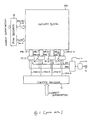
- Fig. 1 schematically shows the above-described one conventional DRAM. It should be noted in this DRAM that bit lines are constructed of main-bit/sub-bit line arrangement, and a single sense amplifier is commonly used by a plurality of sub-bit lines.
- This DRAM owns a memory block MB and a peripheral circuit thereof. This memory block MB will be discussed later in detail with reference to Fig. 2.
- the data read/write amplifier 14 is connected via an input/output buffer 15 to an input/output pin 16, so that data is transmitted between the data read/write amplifier 14 and the input/output pin 16.
- One switch circuit of the switch circuits 10-i is selected by an address in response to a switch selecting signal YSW-i sent from a column decoder 12.
- a word line selecting signal SWL and memory switching signals TG 0 to TG 3 are supplied from a row decoder 13 to the memory block MB.
- the row decoder 13 drives one word line selecting signal SWL 00 based on the address information.
- data of the selected memory cell are read to the respective main bit line pair MBL, MBLb.
- the column decoder 12 selects the main bit line pair MBL, MBLb via one switch circuit 10 to be connected with the data bus pair DB, DBb.
- the input/output buffer 15 output the read data to the input/output pin 16 based upon the data appearing on the selected main bit line pair MBL, MBLb in the data read mode, whereas the data amplifier 14 drives the main bit line pair based on the write data to the input/output pin 16 in the data write mode.
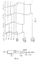
- FIG. 2 there is shown an arrangement related to the main bit line pair MBL-0, MBLb-0 as a portion of the memory block MB.
- This memory block is a so-called "open bit system”.
- Four sub-bit lines SBL 0 to SBL 3 are extended on both sides of a single sub-sense amplifier 17a, while commonly using this sub-sense amplifier 17a.
- the word line SWL is intersected with these bit lines SBL 0 to SBL 3 , and then a DRAM memory cell MC constructed of one transistor and one capacitor is provided with each of cross points.
- the sub-bit lines SBL 0 to SBL 3 are connected via pMOS transistors T TG0 to T TG3 to the sub-sense amplifier 17a, and these transistors T TG0 to T TG3 are turned ON/OFF in response to the memory switching signals TG 0 to TG 3 .
- the sub-sense amplifier 17a includes a precharge circuit P 2 for precharging this one pair of input/output nodes, and NMOS transistors T n20 and T n21 for amplifying the level of the selected sub-bit line.
- This sub-sense amplifier 17a further contains nMOS transistors T n22 to T n25 for controlling connection/disconnection between the selected sub-bit line and main bit line pair MBL-0, MBLb-0.
- the nMOS transistors T n22 and T n23 are conducted by the signal RS when the amplified level of the sub-bit line is transferred to the main bit line, whereas the nMOS transistors T n24 and T n25 are conducted by the signal WS when the data is rewritten.
- a main sense amplifier 18a is connected to the main bit line pair MBL-0 and MBLb-0.
- This main sense amplifier 18a includes a main bit line precharge circuit P 1 , pMOS transistors T p20 , T p21 and nMOS transistors T n26 , T n27 , which are provided between sense amplifier drive lines SAP and SAN, and are connected to form a flip-flop.
- Each of the precharge circuits P 1 and P 2 precharges the input/output node of the corresponding sense amplifier to a Vcc/2-level.
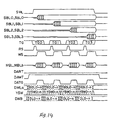
- the precharge circuits P 1 , P 2 become inactive, and one word line, for instance, SWL 00 is selected to become a high level. Furthermore, the switching signal TG 0 becomes a low level. As a result, a memory cell MCO00 located at a cross point between this word line SWL 00 and the sub-bit line SBL 0 is selected, and thus, the potential of the sub-bit line SBL 0 becomes such a potential corresponding to the data stored in this selected memory cell MC 000 . On the other hand, the sub-line line SBL 0 located on the lower side of the sub-sense amplifier 17a holds the precharge level. Accordingly, a potential difference is produced at the input/output node of the sub-sense amplifier 17a.
- the read signal RS becomes active, so that the transistors T n22 and T n23 are conducted. As a consequence, this potential difference is transferred to the main-bit line pair MBL and MBLb.
- the sense amplifier drive lines SAP and SAN become active levels, and the levels of the main bit line pair MBL and MBLb are amplified by the main sense amplifier 18a.
- the read signal RS becomes a low level and the write signal WS becomes a high level, and the respective levels of the main-bit line pair MBL, MBLb are transferred via the transistors T n24 and T n25 to the sub-bit line SBL 0 , so that the data is rewritten into the memory cell MC 000 .
- the addresses to the column decoder 12 are sequentially changed during a time period (T1) when the write signal WS is at the high level to thereby sequentially select the switch circuit 10, so that the data appearing on the main bit line pair MBL, MBLb are successively outputted.
- T1 time period
- the writer signal WS is set to a low level, so that the respective main bit line pair MBL, MBLb are precharged to Vcc/2.
- the memory switching signal TG 1 becomes a high level, so that the data are read out in the continuous manner.
- the respective main bit line pair MBL, MBLb must be precharged so as to be initialized every time the signals for causing the switching signals TG 0 to TG 4 to become the active levels are switched. Accordingly, the data cannot be continuously read from all of the cells connected to the selected word line, so that the rest time period is required in the data reading operation, as indicated by "t 4 " of Fig. 3.
- US-A-4943944 describes a semiconductor memory having dynamic RAM cells wherein data from a plurality of memory cells are transferred in parallel to an output register; while the data are successively read from the register, transfer gates coupled between the bit lines and the register are turned off to allow the bit lines to be precharged to thereby reduce cycle time.
- an object of the present invention is to provide a semiconductor memory device, the reading efficiency of which is further increased, as compared with that of the conventional semiconductor memory device.
- the main bit line As described above, once the data of the main bit line is latched by the latch circuit, the main bit become free no longer the read data of the main-bit line must be held. Accordingly, after the read data has been latched by the latch circuit, the main bit line can be initialized, so that the next sub-bit line can be accessed immediately. As a result, the initialization time period (tl) of the main-bit line does not need.
- Fig. 4 schematically represents a block diagram of a DRAM according to a first embodiment of the present invention. It should be noted that the same reference numerals shown in Fig. 1 will be employed as those for denoting the same or similar constructive units, and explanations thereof are omitted.
- the respective main-bit line pair MBL, MBLb derived from a memory block MB are connected to data latch circuits 1, respectively.
- a data write signal DAWT, a data read signal DART, and a data latch signal DATG are commonly supplied to each of the data latch circuits 1.
- the main bit line pair MBL, MBLb are electrically connected to the data latch circuits 1.
- the respective switch selecting signals YSW are produced by switch selecting circuits 3.
- the switch selecting circuits produce a transfer signal complementary to the switch selecting signal YSW.
- the transfer signal YSWb of the prestages circuit 3 are inputted to the post-staged circuit 3.
- an address information AD, a clock signal CLK, and a reset signal RST are commonly supplied to the switch selecting circuits 3.
- the data read bus DRB and the data write bus DWB are connected to a data read/write amplifier 6, so that the read data/write data are supplied via an input/output buffer 7 between this data read/write amplifier 6 and an input/output pin 8.
- the switch selecting circuits 3 are arranged as described above, all of these switch selecting circuits 3 can be reset by a reset signal RST so that the switch selecting circuits 3 set the signal YSW non-active.
- the switch selecting circuit 3 indicated the address information enforce the signal YSW high level. Therefore the switch selecting circuit 3 sets the transfer signal YSWb to low level.
- the post staged circuit 3 inputs the transfer signal YSWb at the low level and outputs the signal YSW at high level. That is, the switch selecting circuit 3 may function as a shift register. For instance, the switch selecting circuit 3-0 selected to the address information sets the signal YSW 0 to a high level, so that the switch circuit 2-0 is selected.
- the next switch selecting circuit 3-1 is operated. Subsequently, the switch selecting circuits are successively brought into the active conditions, so that the corresponding switch circuits are successively turned ON.
- each data latch circuit 1 includes nMOS transistors MN 1 and MN 2 with respect to the main-bit line pair MBL and MBLb.
- the data latch signal DATG is supplied to gates of these nMOS transistors MN 1 and MN 2 .
- Inverters IV 1 and IV 2 are connected to the transistors MN 1 and MN 2 .
- An nMOS transistor MN 6 is connected with the output of the inverter IV 1 and another nMOS transistor MN 7 is connected with the output of the inverter IV 2 .
- the data read signal DART becomes active, these nMOS transistors MN 6 and MN 7 are activated, so that a flip-flop R 1 is formed by the inverter IV 1 and IV 2 .
- the output of the inverter IV 1 is connected via an inverter IV 3 to the data read line DRL.
- the output of the inverter IV 2 is connected to a dummy inverter IV 4 . It is provided to make the load capacitances of the outputs of the inverters IV 1 and IV 2 equal to each other.
- an inverter IV 5 is provided with the data write line DWL. The output of this inverter IV 5 is connected to the inverter IV 6 and the nMOS transistor MN 3 . The output of the inverter IV 6 is connected to the nMOS transistor MN 4 . Moreover, the inverter IV 6 is connected via a MOS transistor MN5 to the line DWL.
- another flip-flop R 2 is formed by the inverters IV 5 and IV 6 .
- the output of the inverter IV 5 is connected to the main bit line MBLb, and the output of the inverter IV 6 is connected to the main bit line MBL.
- the nMOS transistor MN 5 may function as a small resistor in order to not transfer the high impedance condition of the data write line DWL to the flip-flop R 2 when the write mode is not selected.
- the signal DART becomes an active high level.
- a data latch signal DATG is produced as a one-shot pulse, so that the read data on the main-bit line pair MBL, MBLb is latched in the flip-flop R 1 .
- the transistors MN 6 and MN 7 are under ON state, so that the data of the selected memory cell is written into the flip-flop R 1 .
- the signal DATG is returned to the low level, the transistors MN 1 and MN 2 are turned OFF, so that the main bit line pair is disconnected from the latch circuit 1.
- the output from the flip-flop R 1 namely the output from the inverter IV 1 is transferred via the inverter IV 2 to the data read line DRL.
- the data read signal DART becomes a low level and the data write signal DAWT becomes a high level, so that the write data is latched from the data write line DWL to the flip-flop R 2 .
- This data written into the flip-flop R 2 is transferred to the main-bit line pair MBL, MBLb when the data latch signal DATG becomes the high level.
- the switch circuit 2 includes pMOS transistors M p1 , M p2 , nMOS transistors M n8 , M n9 and inverter IV 7 .
- the transistors M p1 , M n8 are provided between the data read line DRL and the data read bus DRB, and another pair of transistors M p2 and M n9 are provided between the data write line DWL and the data write bus DWB.
- the switch selecting signal YSW is coupled to the gates of the nMOS transistors M n8 , M n9 , whereas a reverse signal of the switch selecting signal YSW is coupled to the gates of the pMOS transistors M p1 , M p2 .
- the switch selecting signal YSW when the switch selecting signal YSW is in a low level, all of these transistors become non-active, so that the signal path between the data read line DRL and the data read bus DRB, and the signal path between the data write line DWL and the data write bus DWB become non-active, respectively. Conversely, when the switch selecting signal YSW is in a high level, all of these transistors become active, so that the signal path between the data read line DRL and the data read bus DRB, and the signal path between the data write line DWL and the data write bus DRB are conducted, and thus the data are transferred through the respective signal paths.
- the switch selecting circuit 3 is arranged by a data flip-flop DFF and an address decoder AD.
- the address decoder AD receives the address information, and when this address decoder AD is selected, the address decoder AD outputs a low level.
- the address decoder AD outputs a high level in any cases other than the above-described case.
- the transfer signal YSWb-1 is inputted via a gate G 3 arranged by pMOS transistors M p3 and M n10 to a NAND circuit NAND 1 .
- the NAND circuit NAND 1 inputs the output from the address decoder AD and the transfer signal YSWb-1, and is connected to a node "S".
- This node “S” is connected via an inverter IV 9 , to the gate G 4 arranged by a pMOS transistor M p6 and an nMOS transistor M n11 .
- This node S is further connected to a gate G 5 arranged by a pMOS transistor M p4 and an nMOS transistor M n12 .
- the output of the inverter IV 11 is connected to another inverter IV 12 .
- the inverters IV 11 and IV 12 output the transfer signal YSWb and the switch selecting signal YSW, respectively.
- the output of the inverter IV 11 is further connected to a NOR circuit NOR 1 .
- the NOR circuit NOR 1 inputs a reset signal RST and the transfer signal YSWb.
- the output of this NOR circuit NOR 1 is connected the gate G 6 arranged by an nMOS transistor M n13 and a pMOS transistor M p5 .
- the gate G 6 is connected to the input of the gate inverter IV 11 .
- a clock signal CLK is entered into the gates G 3 , G 4 , G 5 , G 6 .
- the gates G 3 and G 6 are opened, whereas when the clock signal CLK is in a low level, the gates G 4 and G 5 are opened.
- the NAND circuit NAND 1 When the transfer signal YSWb-1 is in a high level and also the output from the address decoder AD is in a high level, the NAND circuit NAND 1 outputs a low level at the node S in response to the rising edge of the clock signal CLK. Next, the low level at the node S passes through the gate G 5 upon receipt of the falling edge of the clock CLK. As a result, the switch selecting signal YSW is set to a low level, and the transfer signal YSWb is set to a high level.
- the NAND circuit NAND 1 When the address decoder AD becomes a low level, or the level of the transfer signal YSWb-1 becomes a low level, the NAND circuit NAND 1 outputs a high level at the node "S" upon receipt of the rising edge of the clock CLK irrelevant to the other output levels.
- the gate G 5 causes the high level of the node S to pass there through, so that the switch selecting signal YSW is set to a high level and the transfer signal YSWb is set to a low level.
- the NOR circuit NOR 1 When the high level of the reset signal RST is inputted, the NOR circuit NOR 1 necessarily outputs a low level, so that the transfer signal YSWb is set to a high level.
- the switch selecting circuit 3-0 when the switch selecting circuit 3-0 is selected by the address information, the output of the address decoder AD of the circuit 3-0 becomes a low level.
- the switch selecting circuit 3-0 outputs the switch selecting signal YSW-0 with the high level and the transfer signal YSWb-0 with the low level. Accordingly, in response to the switch selecting signal YSW-0 at the high level, the switch circuit 2-0 becomes activated and the data latch circuit 1-0 is connected to the data read/write amplifier 6 electrically to thereby perform the data transfer operation.
- the transfer signal YSWb-0 at the low level is inputted to the switch selecting circuit 3-1 at the post stage, so that the switch selecting circuit 3-1 outputs the switch selecting signal YSW-1 with the high level and the transfer signal YSWb-1 with the low level after 1 clock.
- the switch selecting signal YSW-0 since the transfer signal YSW-3 with the high level is entered into the switch selecting circuit 3-0 and the output of the address decoder AD of the circuit 3-0 turn low level, the switch selecting signal YSW-0 is set to a low level and the transfer signal YSWb-0 is set to a high level in response to the above-described 1 clock.
- the switch circuit 2-0 disconnect the data latch circuit 1-0 with the data read/write amplifier 6 and the switch circuit 2-1 becomes active.
- the transfer signal YSW having the high level is successively outputted from the selected switch selecting circuit to the post-staged switch selecting circuits every 1 clock, so that the data latch circuit 1 is successively connected with the data read/write amplifier 6.
- the information of the memory cell latched in the data latch circuits 1-0, 1-1, 1-2, and 1-3 is read from the memory cell at the selected address in the serial manner.
- the data read signal DART becomes a high level.
- the data of the selected memory cell is read to each of the main-bit line pairs MBL0-3, NBLb0-3.
- the signal WS becomes a high level and the data of main-bit line pair is amplified, the data latch signal DATG is produced in an one shot signal, and then the respective read data are fetched into the data latch circuits 1-0 ⁇ 1-3, and thereafter transferred to the data read line DBL0-3.
- the switch selecting circuit 3-0 is activated by the signal YSW-0 and enforce the switch circuit 2-0 active.
- the read data latched in the latch circuit 1-0 is sequentially started to be read. While this data is read, the respective main-bit line pairs MBL0-3, MBLb0-3 are initialized, and then the signal TG 1 becomes an active level, so that the data appearing on the next sub-bit line SBL1 is sensed and the read data is rewritten.
- the data latch signal DATG is again produced, and the data derived from the memory cell corresponding to the signal TG 1 is latched into the latch circuit 1, so that the data reading operation is continued.
- the initializing period of the main bit line pairs can be masked, so that the data reading operation can be continued without any interrupt.
- the data write signal DAWT becomes an active high level
- the write data are inputted in input/output pin 8 in the serial manner prior to the selection of the word line, and thus these write data are sequentially latched into the latch circuit 1.
- the word line is selected
- the data of the memory cell selected by the word line is sensed and rewritten
- the data latch signal DATG is produced at a time when the write data are collected in the latch circuit 1.
- the write data are transferred to the respective main-bit line pair and then are written into the memory cells.
- the initializing operation is thereafter carried out for the main-bit line pair, since the latch circuit 1 is disconnected, the subsequent write data can be sequentially latched into the latch circuit 1.
- Fig. 10 is a circuit diagram of a data latch signal DATG generating circuit according to the first embodiment.
- Fig. 11 represents a timing chart for the data latch signal DATG generating circuit.
- a counter CA frequency-divides the clock signal CLK to generage timing signals C 1 to C 4 .
- the timing signals C 1 and C 2 are supplied to a NAND circuit D 2 , and an output from this NAND circuit D 2 is controlled in response to a write enable signal WM having an active high level.
- the timing signals C 3 and C 4 are supplied to a NAND circuit D 3 , and an output from this NAND circuit D 3 is controlled in response to a read enable signal RM having an active high level.
- the data latch signal DATG is.
- this data latch signal DATG owns different timings during the data reading operation and the data writing operation. This implies that all of the data are not written into this memory during the data writing operation, but since a portion of data is rewritten by using the original data, after the read data is defined, namely the refresh operation can be sufficiently performed, the data latch signal DATG during the data writing operation is raised.
- Fig. 12 is a circuit diagram for showing data latch signal DATG generating circuit, according to a second embodiment of the present invention, used in the memory.
- the counter CA inputs the clock signal CLK to thereby produce timing signals C 1 and C 4 .
- a data latch signal DATG is generated by a NAND circuit NAND 5 (see Fig. 11).
- the information of the memory cell selected by raising the switch selecting signal YSW during a front half period of the rising condition of the data latch signal DATG is transferred to the data read/write amplifier 6 under such a condition that the levels of the main bit line pair MSL and MSLb can be sufficiently defined.
- the writing operation is performed immediately after the write signal DAWT is raised. Since the data latch signal DATG is raised for a long time period, the level corresponding to the data to be written can be written in to the main bit line pairs MBL and MBLb during a sufficiently long time period. As a result, there is such an advantage that the writing level to the memory cell can be improved.
- the present invention is not limited to the above-described embodiment, but may be modified. For instance, a total number of the sub-bit lines and/or the word lines may be properly changed. Also, only four sets of the main/sub-bit line arrangements are employed in this embodiment. Alternatively, at least two sets of the main/sub-bit line arrangements are sufficient. Furthermore, the above-described embodiment has described that the levels at the respective wire lines were defined at the high levels or the low levels. Alternatively, these levels may be properly changed. Accordingly, the characteristics and the conducting types of these pMOS transistors/nMOS transistors are varied in accordance with the above level changes.
- the present invention can provide such an advantage that the data transfer efficiency can be increased.
Landscapes
- Engineering & Computer Science (AREA)
- Microelectronics & Electronic Packaging (AREA)
- Dram (AREA)
- Semiconductor Memories (AREA)
Claims (8)
- Halbleiterspeichervorrichtung mit:einer Anzahl von Unterbitleitungen (SBL),einem Leseverstärker (17a), der gemeinsam für die Anzahl von Unterbitleitungen vorgesehen ist und ein Datensignal von einer ersten (SBL0) der Anzahl von Unterbitleitungen empfängt,einer Hauptbitleitung (NBL), die operativ mit dem Leseverstärker verbunden ist, zum Empfang der Ausgabe des Leseverstärkers,einer Datenhalteschaltung (1), die zum Halten von Daten vorgesehen ist, die auf der Hauptbitleitung erscheinen, gekennzeichnet durch Schalter (MN1, MN2), die zwischen die Hauptbitleitungen und die Datenhalteschaltung geschaltet sind, die durch ein Datenhaltesignal (DATG) gesteuert werden, um zumindest während der Zeitspanne aus zu sein, in der Daten von einer zweiten (SBL1) der Anzahl von Unterbitleitungen an den Leseverstärker übertragen werden, während auf die Datenhalteschaltung zugegriffen wird, um gehaltene Daten auszulesen.
- Halbleiterspeichervorrichtung nach Anspruch 1,
wobei der Leseverstärker (17a) auf das Datensignal der einen (SBL1) der Anzahl von Bitleitungen antwortet und die Hauptbitleitung (MBL) treibt, während auf die Datenhalteschaltung zugegriffen wird. - Halbleiterspeichervorrichtung nach Anspruch 1,
mit ferner einem zusätzlichen Leseverstärker (18a), der zum Treiben der Hauptbitleitung in Antwort auf die Ausgabe des Leseverstärkers (17a) geschaltet ist, wobei die Datenhalteschaltung (1) aktiviert wird, um die Daten auf der Hauptbitleitung (MBL) zu halten, nachdem der zusätzliche Leseverstärker (18a) die Hauptbitleitung treibt. - Halbleiterspeichervorrichtung mit:einer Anzahl von Unterbitleitungen (SB),einem Leseverstärker (17a), der gemeinsam für die Anzahl von Unterbitleitungen vorgesehen ist, einer Hauptbitleitung (MBL), die mit dem Leseverstärker (17a) verbunden ist,einer Datenhalteschaltung (1), die zeitweilig erste zu beschreibende Daten hält,ersten Mitteln (MN1, MN2) zum Übertragen der ersten Daten von der Datenhalteschaltung (1) an die Hauptbitleitung (MBL), um dabei es dem Leseverstärker (17a) zu ermöglichen, eine erste (SBL0) der Unterbitleitungen in Antwort auf das erste Datum zu treiben, undzweiten Mitteln (MN3, MN4) zum Trennen der Datenhalteschaltung (1) von der Hauptbitleitung (MBL) während die Datenhalteschaltung gesteuert wird, um zweite zu schreibende Daten zu halten, um es dabei dem Leseverstärker (17a) zu ermöglichen, das Treiben einer zweiten (SBL1) der Unterbitleitungen in Abhängigkeit von dem zweiten Datum vorzubereiten.
- Halbleiterspeichervorrichtung nach Anspruch 1,wobei die Anzahl von Unterbitleitungen (SBL) in eine Anzahl von Gruppen mit jeweils einer Anzahl von Unterbitleitungen unterteilt ist,wobei eine Anzahl von Wortleitungen (SWL) vorgesehen ist, die die Unterbitleitungen (SBL) kreuzen,wobei eine Anzahl von Speicherzellen (MC) an Schnittpunkten der Unterbitleitungen (SBL) und der Wortleitungen (SWL) vorgesehen sind,wobei eine Anzahl von Leseverstärkern (17a) gemeinsam zu einer zugeordneten der Gruppen vorgesehen ist, um ein Datensignal von der ersten der Unterbitleitungen, die zu der zugeordneten einen der Gruppe gehört, zum empfangen,wobei eine Anzahl von Hauptbitleitungen (MBL) vorgesehen ist, von denen jede operativ mit einem zugeordneten der Leseverstärker (17a) verbunden ist,wobei eine Anzahl von Datenhalteschaltungen (1) vorgesehen ist, jeweils für eine zugeordnete der Hauptbitleitungen, zum Halten von Daten, die auf der zugeordneten Hauptbitleitungen erscheinen, undwobei eine Anzahl von Schaltern vorgesehen ist, von denen jeder zwischen eine zugeordnete Hauptbitleitung und eine zugeordnete Datenhalteschaltung geschaltet ist.
- Halbleiterspeichervorrichtung nach Anspruch 5,
wobei auf die Datenhalteschaltungen (1) in Folge zugegriffen wird, um die in den Datenhalteschaltungen gespeicherten Daten in Reihe auszulesen. - Halbleiterspeichervorrichtung nach Anspruch 1, mit:einer Anzahl von ersten Unterbitleitungen (SBL),einer Anzahl von zweiten Unterbitleitungen (SBL)ersten und zweiten Leseverstärkern (17a), die jeweils für die Anzahl von ersten und zweiten Unterbitleitungen vorgesehen sind,ersten und zweiten Hauptbitleitungen (MBL-0, MBL-1), die jeweils für die ersten und zweiten Leseverstärker (170) vorgesehen sind,ersten und zweiten Datenhalteschaltungen (1-0, 1-1), die jeweils für die ersten und zweiten Hauptbitleitungen vorgesehen sind,einem Datenlesebus (DRB), der für die ersten und zweiten Datenhalteschaltungen vorgesehen ist,einem Datenschreibbus (DWB), der für die ersten und zweiten Datenhalteschaltungen vorgesehen ist,ersten und zweiten Schaltern, die zwischen die ersten und zweiten Hauptbitleitungen bzw. den ersten und zweiten Halteschaltungen geschaltet sind,Lesemitteln für den ersten Verstärker, die ein erstes Lesedatum von einer ersten der Anzahl von ersten Unterbitleitungen empfangen, wobei der zweite Verstärker ein zweites Lesedatum von der ersten der Anzahl von Unterbitleitungen empfängt, die erste Datenhalteschaltung das erste Lesedatum hält, das auf der ersten Hauptbitleitung erscheint, die zweite Datenhalteschaltung das zweite Lesedatum hält, das auf den zweiten Hauptbitleitungen erscheint, und von der ersten der Anzahl von ersten Unterbitleitungen auf eine zweite umschaltet und von der ersten der Anzahl von zweiten Unterbitleitungen zu einer zweiten umschaltet, um die zweite der Anzahl von ersten und zweiten Unterbitleitungen anzusprechen, während auf die ersten und zweiten Datenhalteschaltungen (1-0, 1-1) zugegriffen wird, um die ersten und zweiten Lesedaten, die in der ersten und der zweiten Datenhalteschaltung gehalten sind, auf den Datenlesebus (DRB) auszulesen,Schreibmitteln zum Übertragen eines ersten Schreibdatums, das in der ersten Datenhalteschaltung (1-0) gehalten ist, über die erste Hauptbitleitung (MBL-0) auf die erste der Anzahl von ersten Unterbitleitungen und um ein zweites Schreibdatum, das in der zweiten Datenhalteschaltung (1-1) gehalten ist, über die zweite Hauptbitleitung (MBL-1) zu der ersten der Anzahl von zweiten Unterbitleitungen zu übertragen und von der ersten der Anzahl von ersten Unterbitleitungen auf eine zweite und von der ersten der Anzahl von zweiten Bitleitungen auf eine zweite umzuschalten, um auf die zweite der Anzahl von ersten und zweiten Unterbitleitungen zuzugreifen, während auf die erste und zweite Datenhalteschaltung (1-0, 1-1) zugegriffen wird, um ein drittes Schreibdatum und ein viertes Schreibdatum, die in die zweite der Anzahl von ersten und zweiten Unterbitleitungen zu schreiben sind, zu halten.
- Halbleiterspeichervorrichtung nach Anspruch 1,
wobei die Datenhalteschaltung das Datenhaltesignal (DATG), ein Lesesignal (DART) und ein Schreibsignal (DAWT) eingibt, wobei die Datenhalteschaltungen (1) ein erstes Flip-Flop (R1) aufweist, das durch ein aktives Lesesignal aktiviert wird und ein Lesedatum hält, wenn das Datenhaltesignal (DATG) aktiv wird, während das Lesesignal aktiv ist, ein zweites Flip-Flop (R2) das ein auf einer Datenschreibleitung erscheinendes Schreibdatum durch ein aktives Schreibsignal (DAWT) hält und das gehaltene Datum des zweiten Flip-Flops (R2) auf die Hauptbitleitung überträgt, wenn das Datenhaltesignal (DAGT) aktiv wird, während das Schreibsignal (DAWT) aktiv ist.
Applications Claiming Priority (3)
| Application Number | Priority Date | Filing Date | Title |
|---|---|---|---|
| JP7236508A JP2900854B2 (ja) | 1995-09-14 | 1995-09-14 | 半導体記憶装置 |
| JP23650895 | 1995-09-14 | ||
| JP236508/95 | 1995-09-14 |
Publications (3)
| Publication Number | Publication Date |
|---|---|
| EP0791932A2 EP0791932A2 (de) | 1997-08-27 |
| EP0791932A3 EP0791932A3 (de) | 1998-01-14 |
| EP0791932B1 true EP0791932B1 (de) | 2002-03-13 |
Family
ID=17001763
Family Applications (1)
| Application Number | Title | Priority Date | Filing Date |
|---|---|---|---|
| EP96114668A Expired - Lifetime EP0791932B1 (de) | 1995-09-14 | 1996-09-12 | Halbleiterspeicheranordnung mit Haupt- und Nebenbitleitungsanordnung |
Country Status (6)
| Country | Link |
|---|---|
| US (1) | US5732026A (de) |
| EP (1) | EP0791932B1 (de) |
| JP (1) | JP2900854B2 (de) |
| KR (1) | KR100225826B1 (de) |
| DE (1) | DE69619793T2 (de) |
| TW (1) | TW360972B (de) |
Families Citing this family (10)
| Publication number | Priority date | Publication date | Assignee | Title |
|---|---|---|---|---|
| US6009024A (en) * | 1997-03-27 | 1999-12-28 | Matsushita Electric Industrial Co., Ltd. | Semiconductor memory |
| JPH11110967A (ja) * | 1997-10-01 | 1999-04-23 | Nec Corp | 半導体メモリ装置 |
| JP2000090659A (ja) * | 1998-09-10 | 2000-03-31 | Nec Corp | 半導体記憶装置 |
| KR100487918B1 (ko) * | 2002-08-30 | 2005-05-09 | 주식회사 하이닉스반도체 | 불휘발성 강유전체 메모리 장치 |
| US7349266B2 (en) * | 2004-06-10 | 2008-03-25 | Freescale Semiconductor, Inc. | Memory device with a data hold latch |
| US7289369B2 (en) * | 2005-04-18 | 2007-10-30 | International Business Machines Corporation | DRAM hierarchical data path |
| US7719905B2 (en) * | 2007-05-17 | 2010-05-18 | Hynix Semiconductor, Inc. | Semiconductor memory device |
| US9053817B2 (en) * | 2013-03-15 | 2015-06-09 | Taiwan Semiconductor Manufacturing Company, Ltd. | Amplifier |
| US11302383B2 (en) | 2018-12-10 | 2022-04-12 | Etron Technology, Inc. | Dynamic memory with sustainable storage architecture |
| US11798613B2 (en) | 2018-12-10 | 2023-10-24 | Etron Technology, Inc. | Dynamic memory with long retention time |
Family Cites Families (8)
| Publication number | Priority date | Publication date | Assignee | Title |
|---|---|---|---|---|
| US4344156A (en) * | 1980-10-10 | 1982-08-10 | Inmos Corporation | High speed data transfer for a semiconductor memory |
| JP2579974B2 (ja) * | 1987-11-25 | 1997-02-12 | 株式会社東芝 | 半導体記憶装置 |
| JP2713929B2 (ja) * | 1987-11-25 | 1998-02-16 | 株式会社東芝 | 半導体記憶装置 |
| US4943944A (en) * | 1987-11-25 | 1990-07-24 | Kabushiki Kaisha Toshiba | Semiconductor memory using dynamic ram cells |
| JP2591010B2 (ja) * | 1988-01-29 | 1997-03-19 | 日本電気株式会社 | シリアルアクセスメモリ装置 |
| JP2611504B2 (ja) * | 1990-06-15 | 1997-05-21 | 日本電気株式会社 | 半導体メモリ |
| JPH06203552A (ja) * | 1991-11-18 | 1994-07-22 | Toshiba Corp | ダイナミック型半導体記憶装置 |
| JPH05250875A (ja) * | 1992-02-27 | 1993-09-28 | Nec Corp | 半導体記憶装置 |
-
1995
- 1995-09-14 JP JP7236508A patent/JP2900854B2/ja not_active Expired - Fee Related
-
1996
- 1996-09-12 EP EP96114668A patent/EP0791932B1/de not_active Expired - Lifetime
- 1996-09-12 DE DE69619793T patent/DE69619793T2/de not_active Expired - Fee Related
- 1996-09-13 US US08/713,692 patent/US5732026A/en not_active Expired - Fee Related
- 1996-09-13 KR KR1019960039600A patent/KR100225826B1/ko not_active IP Right Cessation
- 1996-09-14 TW TW085111234A patent/TW360972B/zh active
Also Published As
| Publication number | Publication date |
|---|---|
| EP0791932A3 (de) | 1998-01-14 |
| DE69619793T2 (de) | 2002-11-21 |
| JPH0982086A (ja) | 1997-03-28 |
| TW360972B (en) | 1999-06-11 |
| JP2900854B2 (ja) | 1999-06-02 |
| KR970017610A (ko) | 1997-04-30 |
| KR100225826B1 (ko) | 1999-10-15 |
| US5732026A (en) | 1998-03-24 |
| EP0791932A2 (de) | 1997-08-27 |
| DE69619793D1 (de) | 2002-04-18 |
Similar Documents
| Publication | Publication Date | Title |
|---|---|---|
| US5568428A (en) | Memory device and serial-parallel data transform circuit | |
| US4879692A (en) | Dynamic memory circuit with improved sensing scheme | |
| US5410505A (en) | Semiconductor memory device having a memory cell unit including a plurality of transistors connected in series | |
| EP0264929B1 (de) | Halbleiterspeicheranordnung mit verbesserter Bitzeilenordnung | |
| US5892724A (en) | NAND-type dynamic RAM having temporary storage register and sense amplifier coupled to multi-open bit lines | |
| JP2685357B2 (ja) | 半導体記憶装置 | |
| JPS61160898A (ja) | 半導体記憶装置 | |
| JP2705590B2 (ja) | 半導体記憶装置 | |
| US4979145A (en) | Structure and method for improving high speed data rate in a DRAM | |
| EP0791932B1 (de) | Halbleiterspeicheranordnung mit Haupt- und Nebenbitleitungsanordnung | |
| US4451906A (en) | Dynamic type memory device having improved operation speed | |
| JP2604276B2 (ja) | 半導体記憶装置 | |
| JP2795074B2 (ja) | ダイナミックram | |
| KR950006962B1 (ko) | 반도체 기억 장치 | |
| EP0573046B1 (de) | Halbleiterspeicheranordnung mit zwischen Speicherzellenmatrizen geteiltem Einzeldatenleitungspaar | |
| US6359825B1 (en) | Dynamic memory with increased access speed and reduced chip area | |
| US5463584A (en) | Semiconductor memory device | |
| US5894440A (en) | Semiconductor memory device and data transferring structure and method therein | |
| JP2993671B2 (ja) | 半導体記憶装置 | |
| JPH0787035B2 (ja) | 半導体記億装置 | |
| JPS6142794A (ja) | 半導体記憶装置のセンスアンプ系 | |
| KR0158002B1 (ko) | 의사 디지트 선을 갖는 반도체 메모리 장치 | |
| US20030179620A1 (en) | Semiconductor memory device | |
| JP2668165B2 (ja) | 半導体記憶装置 | |
| US6141235A (en) | Stacked cache memory system and method |
Legal Events
| Date | Code | Title | Description |
|---|---|---|---|
| PUAI | Public reference made under article 153(3) epc to a published international application that has entered the european phase |
Free format text: ORIGINAL CODE: 0009012 |
|
| AK | Designated contracting states |
Kind code of ref document: A2 Designated state(s): DE FR GB |
|
| PUAL | Search report despatched |
Free format text: ORIGINAL CODE: 0009013 |
|
| AK | Designated contracting states |
Kind code of ref document: A3 Designated state(s): DE FR GB |
|
| 17P | Request for examination filed |
Effective date: 19971204 |
|
| 17Q | First examination report despatched |
Effective date: 20000524 |
|
| GRAG | Despatch of communication of intention to grant |
Free format text: ORIGINAL CODE: EPIDOS AGRA |
|
| GRAG | Despatch of communication of intention to grant |
Free format text: ORIGINAL CODE: EPIDOS AGRA |
|
| GRAH | Despatch of communication of intention to grant a patent |
Free format text: ORIGINAL CODE: EPIDOS IGRA |
|
| GRAH | Despatch of communication of intention to grant a patent |
Free format text: ORIGINAL CODE: EPIDOS IGRA |
|
| REG | Reference to a national code |
Ref country code: GB Ref legal event code: IF02 |
|
| GRAA | (expected) grant |
Free format text: ORIGINAL CODE: 0009210 |
|
| AK | Designated contracting states |
Kind code of ref document: B1 Designated state(s): DE FR GB |
|
| REF | Corresponds to: |
Ref document number: 69619793 Country of ref document: DE Date of ref document: 20020418 |
|
| ET | Fr: translation filed | ||
| PLBE | No opposition filed within time limit |
Free format text: ORIGINAL CODE: 0009261 |
|
| STAA | Information on the status of an ep patent application or granted ep patent |
Free format text: STATUS: NO OPPOSITION FILED WITHIN TIME LIMIT |
|
| 26N | No opposition filed |
Effective date: 20021216 |
|
| REG | Reference to a national code |
Ref country code: GB Ref legal event code: 732E |
|
| REG | Reference to a national code |
Ref country code: FR Ref legal event code: TP |
|
| PGFP | Annual fee paid to national office [announced via postgrant information from national office to epo] |
Ref country code: GB Payment date: 20040908 Year of fee payment: 9 Ref country code: FR Payment date: 20040908 Year of fee payment: 9 |
|
| PGFP | Annual fee paid to national office [announced via postgrant information from national office to epo] |
Ref country code: DE Payment date: 20040909 Year of fee payment: 9 |
|
| PG25 | Lapsed in a contracting state [announced via postgrant information from national office to epo] |
Ref country code: GB Free format text: LAPSE BECAUSE OF NON-PAYMENT OF DUE FEES Effective date: 20050912 |
|
| PG25 | Lapsed in a contracting state [announced via postgrant information from national office to epo] |
Ref country code: DE Free format text: LAPSE BECAUSE OF NON-PAYMENT OF DUE FEES Effective date: 20060401 |
|
| GBPC | Gb: european patent ceased through non-payment of renewal fee |
Effective date: 20050912 |
|
| PG25 | Lapsed in a contracting state [announced via postgrant information from national office to epo] |
Ref country code: FR Free format text: LAPSE BECAUSE OF NON-PAYMENT OF DUE FEES Effective date: 20060531 |
|
| REG | Reference to a national code |
Ref country code: FR Ref legal event code: ST Effective date: 20060531 |