EP0766321B1 - Method of producing a photovoltaic device - Google Patents
Method of producing a photovoltaic device Download PDFInfo
- Publication number
- EP0766321B1 EP0766321B1 EP96115386A EP96115386A EP0766321B1 EP 0766321 B1 EP0766321 B1 EP 0766321B1 EP 96115386 A EP96115386 A EP 96115386A EP 96115386 A EP96115386 A EP 96115386A EP 0766321 B1 EP0766321 B1 EP 0766321B1
- Authority
- EP
- European Patent Office
- Prior art keywords
- layer
- substrate
- gas
- photovoltaic device
- deposition chamber
- Prior art date
- Legal status (The legal status is an assumption and is not a legal conclusion. Google has not performed a legal analysis and makes no representation as to the accuracy of the status listed.)
- Expired - Lifetime
Links
- 238000000034 method Methods 0.000 title claims description 209
- 239000007789 gas Substances 0.000 claims description 1191
- 239000000758 substrate Substances 0.000 claims description 1010
- 238000000151 deposition Methods 0.000 claims description 604
- XLOMVQKBTHCTTD-UHFFFAOYSA-N Zinc monoxide Chemical compound [Zn]=O XLOMVQKBTHCTTD-UHFFFAOYSA-N 0.000 claims description 372
- 230000002708 enhancing effect Effects 0.000 claims description 279
- 239000011787 zinc oxide Substances 0.000 claims description 186
- 239000000463 material Substances 0.000 claims description 153
- 230000015572 biosynthetic process Effects 0.000 claims description 132
- 239000004065 semiconductor Substances 0.000 claims description 90
- UFHFLCQGNIYNRP-UHFFFAOYSA-N Hydrogen Chemical compound [H][H] UFHFLCQGNIYNRP-UHFFFAOYSA-N 0.000 claims description 33
- XKRFYHLGVUSROY-UHFFFAOYSA-N Argon Chemical compound [Ar] XKRFYHLGVUSROY-UHFFFAOYSA-N 0.000 claims description 26
- 229910052786 argon Inorganic materials 0.000 claims description 14
- 229910052734 helium Inorganic materials 0.000 claims description 14
- 239000001307 helium Substances 0.000 claims description 13
- SWQJXJOGLNCZEY-UHFFFAOYSA-N helium atom Chemical compound [He] SWQJXJOGLNCZEY-UHFFFAOYSA-N 0.000 claims description 13
- 229910052709 silver Inorganic materials 0.000 claims description 12
- XUIMIQQOPSSXEZ-UHFFFAOYSA-N Silicon Chemical group [Si] XUIMIQQOPSSXEZ-UHFFFAOYSA-N 0.000 claims description 9
- 229910052804 chromium Inorganic materials 0.000 claims description 8
- 229910052802 copper Inorganic materials 0.000 claims description 8
- 239000013078 crystal Substances 0.000 claims description 8
- 229910052759 nickel Inorganic materials 0.000 claims description 8
- 229910052742 iron Inorganic materials 0.000 claims description 7
- 239000004332 silver Substances 0.000 claims description 3
- 238000009751 slip forming Methods 0.000 claims description 3
- 229910000676 Si alloy Inorganic materials 0.000 claims 2
- CSDREXVUYHZDNP-UHFFFAOYSA-N alumanylidynesilicon Chemical compound [Al].[Si] CSDREXVUYHZDNP-UHFFFAOYSA-N 0.000 claims 2
- 239000010410 layer Substances 0.000 description 1835
- 230000008021 deposition Effects 0.000 description 587
- 238000006243 chemical reaction Methods 0.000 description 142
- 238000004519 manufacturing process Methods 0.000 description 118
- BLRPTPMANUNPDV-UHFFFAOYSA-N Silane Chemical compound [SiH4] BLRPTPMANUNPDV-UHFFFAOYSA-N 0.000 description 108
- 239000000112 cooling gas Substances 0.000 description 101
- 238000005452 bending Methods 0.000 description 97
- 238000012360 testing method Methods 0.000 description 96
- 229910018125 Al-Si Inorganic materials 0.000 description 85
- 229910018520 Al—Si Inorganic materials 0.000 description 85
- 229910007264 Si2H6 Inorganic materials 0.000 description 59
- PZPGRFITIJYNEJ-UHFFFAOYSA-N disilane Chemical compound [SiH3][SiH3] PZPGRFITIJYNEJ-UHFFFAOYSA-N 0.000 description 59
- 230000007613 environmental effect Effects 0.000 description 58
- 229910001220 stainless steel Inorganic materials 0.000 description 56
- 239000010935 stainless steel Substances 0.000 description 56
- CSCPPACGZOOCGX-UHFFFAOYSA-N Acetone Chemical compound CC(C)=O CSCPPACGZOOCGX-UHFFFAOYSA-N 0.000 description 52
- KFZMGEQAYNKOFK-UHFFFAOYSA-N Isopropanol Chemical compound CC(C)O KFZMGEQAYNKOFK-UHFFFAOYSA-N 0.000 description 52
- 229910021417 amorphous silicon Inorganic materials 0.000 description 50
- XYFCBTPGUUZFHI-UHFFFAOYSA-N Phosphine Chemical compound P XYFCBTPGUUZFHI-UHFFFAOYSA-N 0.000 description 48
- 238000001755 magnetron sputter deposition Methods 0.000 description 43
- 230000008569 process Effects 0.000 description 42
- 238000004544 sputter deposition Methods 0.000 description 37
- 229910010271 silicon carbide Inorganic materials 0.000 description 36
- IUVCFHHAEHNCFT-INIZCTEOSA-N 2-[(1s)-1-[4-amino-3-(3-fluoro-4-propan-2-yloxyphenyl)pyrazolo[3,4-d]pyrimidin-1-yl]ethyl]-6-fluoro-3-(3-fluorophenyl)chromen-4-one Chemical compound C1=C(F)C(OC(C)C)=CC=C1C(C1=C(N)N=CN=C11)=NN1[C@@H](C)C1=C(C=2C=C(F)C=CC=2)C(=O)C2=CC(F)=CC=C2O1 IUVCFHHAEHNCFT-INIZCTEOSA-N 0.000 description 35
- 238000011156 evaluation Methods 0.000 description 35
- VNWKTOKETHGBQD-UHFFFAOYSA-N methane Chemical compound C VNWKTOKETHGBQD-UHFFFAOYSA-N 0.000 description 34
- 229910021424 microcrystalline silicon Inorganic materials 0.000 description 34
- 239000010408 film Substances 0.000 description 33
- QUZPNFFHZPRKJD-UHFFFAOYSA-N germane Chemical compound [GeH4] QUZPNFFHZPRKJD-UHFFFAOYSA-N 0.000 description 33
- 229910052986 germanium hydride Inorganic materials 0.000 description 33
- 238000012545 processing Methods 0.000 description 33
- 229910052751 metal Inorganic materials 0.000 description 32
- 238000001771 vacuum deposition Methods 0.000 description 32
- 239000002184 metal Substances 0.000 description 31
- 238000005259 measurement Methods 0.000 description 30
- 238000004506 ultrasonic cleaning Methods 0.000 description 26
- 238000010790 dilution Methods 0.000 description 24
- 239000012895 dilution Substances 0.000 description 24
- 238000007602 hot air drying Methods 0.000 description 24
- 239000000843 powder Substances 0.000 description 24
- 229910000577 Silicon-germanium Inorganic materials 0.000 description 23
- 238000012546 transfer Methods 0.000 description 23
- 229910052739 hydrogen Inorganic materials 0.000 description 19
- 239000001257 hydrogen Substances 0.000 description 15
- 238000005478 sputtering type Methods 0.000 description 15
- 238000010438 heat treatment Methods 0.000 description 13
- IJGRMHOSHXDMSA-UHFFFAOYSA-N Atomic nitrogen Chemical compound N#N IJGRMHOSHXDMSA-UHFFFAOYSA-N 0.000 description 12
- 125000005843 halogen group Chemical group 0.000 description 12
- 238000002360 preparation method Methods 0.000 description 12
- 150000001875 compounds Chemical class 0.000 description 11
- 238000005268 plasma chemical vapour deposition Methods 0.000 description 11
- 238000007740 vapor deposition Methods 0.000 description 11
- XEEYBQQBJWHFJM-UHFFFAOYSA-N Iron Chemical compound [Fe] XEEYBQQBJWHFJM-UHFFFAOYSA-N 0.000 description 10
- 229910052732 germanium Inorganic materials 0.000 description 10
- GNPVGFCGXDBREM-UHFFFAOYSA-N germanium atom Chemical compound [Ge] GNPVGFCGXDBREM-UHFFFAOYSA-N 0.000 description 10
- -1 polyethylene terephthalate Polymers 0.000 description 10
- 230000001965 increasing effect Effects 0.000 description 9
- 238000000926 separation method Methods 0.000 description 9
- 238000004804 winding Methods 0.000 description 9
- 229910003915 SiCl2H2 Inorganic materials 0.000 description 8
- 229910052782 aluminium Inorganic materials 0.000 description 8
- XOLBLPGZBRYERU-UHFFFAOYSA-N tin dioxide Chemical compound O=[Sn]=O XOLBLPGZBRYERU-UHFFFAOYSA-N 0.000 description 8
- OKTJSMMVPCPJKN-UHFFFAOYSA-N Carbon Chemical compound [C] OKTJSMMVPCPJKN-UHFFFAOYSA-N 0.000 description 7
- 229910052799 carbon Inorganic materials 0.000 description 7
- 239000010949 copper Substances 0.000 description 7
- 229910021478 group 5 element Inorganic materials 0.000 description 7
- 229910052736 halogen Inorganic materials 0.000 description 7
- 150000002367 halogens Chemical class 0.000 description 7
- 230000006872 improvement Effects 0.000 description 7
- 239000011261 inert gas Substances 0.000 description 7
- 230000007246 mechanism Effects 0.000 description 7
- 238000002310 reflectometry Methods 0.000 description 7
- 229910021364 Al-Si alloy Inorganic materials 0.000 description 6
- 229910004016 SiF2 Inorganic materials 0.000 description 6
- 229910045601 alloy Inorganic materials 0.000 description 6
- 239000000956 alloy Substances 0.000 description 6
- QVGXLLKOCUKJST-UHFFFAOYSA-N atomic oxygen Chemical compound [O] QVGXLLKOCUKJST-UHFFFAOYSA-N 0.000 description 6
- 229910052757 nitrogen Inorganic materials 0.000 description 6
- 239000001301 oxygen Substances 0.000 description 6
- 229910052760 oxygen Inorganic materials 0.000 description 6
- 239000010409 thin film Substances 0.000 description 6
- 101000639987 Homo sapiens Stearoyl-CoA desaturase 5 Proteins 0.000 description 5
- 101100309606 Saccharomyces cerevisiae (strain ATCC 204508 / S288c) SCD6 gene Proteins 0.000 description 5
- 102100033930 Stearoyl-CoA desaturase 5 Human genes 0.000 description 5
- 229910052796 boron Inorganic materials 0.000 description 5
- 238000001816 cooling Methods 0.000 description 5
- 239000012535 impurity Substances 0.000 description 5
- 239000007769 metal material Substances 0.000 description 5
- 238000002156 mixing Methods 0.000 description 5
- 229910052698 phosphorus Inorganic materials 0.000 description 5
- 230000009467 reduction Effects 0.000 description 5
- 229910052710 silicon Inorganic materials 0.000 description 5
- 239000010703 silicon Substances 0.000 description 5
- LEVVHYCKPQWKOP-UHFFFAOYSA-N [Si].[Ge] Chemical compound [Si].[Ge] LEVVHYCKPQWKOP-UHFFFAOYSA-N 0.000 description 4
- 238000000137 annealing Methods 0.000 description 4
- 238000009792 diffusion process Methods 0.000 description 4
- 229910052737 gold Inorganic materials 0.000 description 4
- 229910021480 group 4 element Inorganic materials 0.000 description 4
- 150000002431 hydrogen Chemical class 0.000 description 4
- 125000004435 hydrogen atom Chemical group [H]* 0.000 description 4
- PJXISJQVUVHSOJ-UHFFFAOYSA-N indium(III) oxide Inorganic materials [O-2].[O-2].[O-2].[In+3].[In+3] PJXISJQVUVHSOJ-UHFFFAOYSA-N 0.000 description 4
- 230000003647 oxidation Effects 0.000 description 4
- 238000007254 oxidation reaction Methods 0.000 description 4
- 230000005855 radiation Effects 0.000 description 4
- 229910000077 silane Inorganic materials 0.000 description 4
- HBMJWWWQQXIZIP-UHFFFAOYSA-N silicon carbide Chemical compound [Si+]#[C-] HBMJWWWQQXIZIP-UHFFFAOYSA-N 0.000 description 4
- IKOKHHBZFDFMJW-UHFFFAOYSA-N 2-[4-[2-(2,3-dihydro-1H-inden-2-ylamino)pyrimidin-5-yl]-3-(2-morpholin-4-ylethoxy)pyrazol-1-yl]-1-(2,4,6,7-tetrahydrotriazolo[4,5-c]pyridin-5-yl)ethanone Chemical compound C1C(CC2=CC=CC=C12)NC1=NC=C(C=N1)C=1C(=NN(C=1)CC(=O)N1CC2=C(CC1)NN=N2)OCCN1CCOCC1 IKOKHHBZFDFMJW-UHFFFAOYSA-N 0.000 description 3
- 229910052785 arsenic Inorganic materials 0.000 description 3
- 125000004429 atom Chemical group 0.000 description 3
- 239000012159 carrier gas Substances 0.000 description 3
- 230000015556 catabolic process Effects 0.000 description 3
- 230000007423 decrease Effects 0.000 description 3
- 238000006731 degradation reaction Methods 0.000 description 3
- 238000005137 deposition process Methods 0.000 description 3
- MGNHOGAVECORPT-UHFFFAOYSA-N difluorosilicon Chemical compound F[Si]F MGNHOGAVECORPT-UHFFFAOYSA-N 0.000 description 3
- 238000007599 discharging Methods 0.000 description 3
- 238000010894 electron beam technology Methods 0.000 description 3
- 230000005284 excitation Effects 0.000 description 3
- 229910052733 gallium Inorganic materials 0.000 description 3
- 150000002739 metals Chemical class 0.000 description 3
- 230000003287 optical effect Effects 0.000 description 3
- 229910021420 polycrystalline silicon Inorganic materials 0.000 description 3
- 238000010926 purge Methods 0.000 description 3
- ZOXJGFHDIHLPTG-UHFFFAOYSA-N Boron Chemical compound [B] ZOXJGFHDIHLPTG-UHFFFAOYSA-N 0.000 description 2
- 229910004014 SiF4 Inorganic materials 0.000 description 2
- 229910003811 SiGeC Inorganic materials 0.000 description 2
- VYPSYNLAJGMNEJ-UHFFFAOYSA-N Silicium dioxide Chemical compound O=[Si]=O VYPSYNLAJGMNEJ-UHFFFAOYSA-N 0.000 description 2
- BQCADISMDOOEFD-UHFFFAOYSA-N Silver Chemical compound [Ag] BQCADISMDOOEFD-UHFFFAOYSA-N 0.000 description 2
- 239000012790 adhesive layer Substances 0.000 description 2
- PNEYBMLMFCGWSK-UHFFFAOYSA-N aluminium oxide Inorganic materials [O-2].[O-2].[O-2].[Al+3].[Al+3] PNEYBMLMFCGWSK-UHFFFAOYSA-N 0.000 description 2
- VSCWAEJMTAWNJL-UHFFFAOYSA-K aluminium trichloride Chemical compound Cl[Al](Cl)Cl VSCWAEJMTAWNJL-UHFFFAOYSA-K 0.000 description 2
- 229910052787 antimony Inorganic materials 0.000 description 2
- 229910052797 bismuth Inorganic materials 0.000 description 2
- CXKCTMHTOKXKQT-UHFFFAOYSA-N cadmium oxide Inorganic materials [Cd]=O CXKCTMHTOKXKQT-UHFFFAOYSA-N 0.000 description 2
- 230000008859 change Effects 0.000 description 2
- 239000011651 chromium Substances 0.000 description 2
- 239000000470 constituent Substances 0.000 description 2
- 238000005336 cracking Methods 0.000 description 2
- KBDJQNUZLNUGDS-UHFFFAOYSA-N dibromosilicon Chemical compound Br[Si]Br KBDJQNUZLNUGDS-UHFFFAOYSA-N 0.000 description 2
- 229910001873 dinitrogen Inorganic materials 0.000 description 2
- 230000000694 effects Effects 0.000 description 2
- 229920006332 epoxy adhesive Polymers 0.000 description 2
- 230000001747 exhibiting effect Effects 0.000 description 2
- 239000000835 fiber Substances 0.000 description 2
- 229910000078 germane Inorganic materials 0.000 description 2
- 238000005286 illumination Methods 0.000 description 2
- 229910052738 indium Inorganic materials 0.000 description 2
- PSCMQHVBLHHWTO-UHFFFAOYSA-K indium(iii) chloride Chemical compound Cl[In](Cl)Cl PSCMQHVBLHHWTO-UHFFFAOYSA-K 0.000 description 2
- 229910044991 metal oxide Inorganic materials 0.000 description 2
- 150000004706 metal oxides Chemical class 0.000 description 2
- 239000013080 microcrystalline material Substances 0.000 description 2
- 239000000203 mixture Substances 0.000 description 2
- 229910052750 molybdenum Inorganic materials 0.000 description 2
- PXHVJJICTQNCMI-UHFFFAOYSA-N nickel Substances [Ni] PXHVJJICTQNCMI-UHFFFAOYSA-N 0.000 description 2
- 239000011574 phosphorus Substances 0.000 description 2
- 238000007747 plating Methods 0.000 description 2
- 229920005989 resin Polymers 0.000 description 2
- 239000011347 resin Substances 0.000 description 2
- 230000004044 response Effects 0.000 description 2
- 238000005096 rolling process Methods 0.000 description 2
- 229910052814 silicon oxide Inorganic materials 0.000 description 2
- ABTOQLMXBSRXSM-UHFFFAOYSA-N silicon tetrafluoride Chemical compound F[Si](F)(F)F ABTOQLMXBSRXSM-UHFFFAOYSA-N 0.000 description 2
- 239000010944 silver (metal) Substances 0.000 description 2
- 238000005507 spraying Methods 0.000 description 2
- 229910052716 thallium Inorganic materials 0.000 description 2
- 238000002834 transmittance Methods 0.000 description 2
- 238000003466 welding Methods 0.000 description 2
- 229910001316 Ag alloy Inorganic materials 0.000 description 1
- 229910000838 Al alloy Inorganic materials 0.000 description 1
- 229910017083 AlN Inorganic materials 0.000 description 1
- 229910021630 Antimony pentafluoride Inorganic materials 0.000 description 1
- 229910017011 AsBr3 Inorganic materials 0.000 description 1
- 229910017009 AsCl3 Inorganic materials 0.000 description 1
- 229910017050 AsF3 Inorganic materials 0.000 description 1
- 229910017049 AsF5 Inorganic materials 0.000 description 1
- 229910015844 BCl3 Inorganic materials 0.000 description 1
- 229920000049 Carbon (fiber) Polymers 0.000 description 1
- RYGMFSIKBFXOCR-UHFFFAOYSA-N Copper Chemical compound [Cu] RYGMFSIKBFXOCR-UHFFFAOYSA-N 0.000 description 1
- 229910000881 Cu alloy Inorganic materials 0.000 description 1
- MYMOFIZGZYHOMD-UHFFFAOYSA-N Dioxygen Chemical compound O=O MYMOFIZGZYHOMD-UHFFFAOYSA-N 0.000 description 1
- LFQSCWFLJHTTHZ-UHFFFAOYSA-N Ethanol Chemical compound CCO LFQSCWFLJHTTHZ-UHFFFAOYSA-N 0.000 description 1
- 229910000640 Fe alloy Inorganic materials 0.000 description 1
- 229910005267 GaCl3 Inorganic materials 0.000 description 1
- 229910006158 GeF2 Inorganic materials 0.000 description 1
- 229910006160 GeF4 Inorganic materials 0.000 description 1
- OKKJLVBELUTLKV-UHFFFAOYSA-N Methanol Chemical compound OC OKKJLVBELUTLKV-UHFFFAOYSA-N 0.000 description 1
- JCXJVPUVTGWSNB-UHFFFAOYSA-N Nitrogen dioxide Chemical compound O=[N]=O JCXJVPUVTGWSNB-UHFFFAOYSA-N 0.000 description 1
- GQPLMRYTRLFLPF-UHFFFAOYSA-N Nitrous Oxide Chemical compound [O-][N+]#N GQPLMRYTRLFLPF-UHFFFAOYSA-N 0.000 description 1
- 229910020667 PBr3 Inorganic materials 0.000 description 1
- 229910020656 PBr5 Inorganic materials 0.000 description 1
- OAICVXFJPJFONN-UHFFFAOYSA-N Phosphorus Chemical compound [P] OAICVXFJPJFONN-UHFFFAOYSA-N 0.000 description 1
- 239000004952 Polyamide Substances 0.000 description 1
- 239000004642 Polyimide Substances 0.000 description 1
- 229910007245 Si2Cl6 Inorganic materials 0.000 description 1
- 229910007260 Si2F6 Inorganic materials 0.000 description 1
- 229910005096 Si3H8 Inorganic materials 0.000 description 1
- 229910052581 Si3N4 Inorganic materials 0.000 description 1
- 229910003676 SiBr4 Inorganic materials 0.000 description 1
- 229910003910 SiCl4 Inorganic materials 0.000 description 1
- 229910003818 SiH2Cl2 Inorganic materials 0.000 description 1
- 229910003828 SiH3 Inorganic materials 0.000 description 1
- 229910003822 SiHCl3 Inorganic materials 0.000 description 1
- 229910017875 a-SiN Inorganic materials 0.000 description 1
- 230000004913 activation Effects 0.000 description 1
- XAGFODPZIPBFFR-UHFFFAOYSA-N aluminium Chemical compound [Al] XAGFODPZIPBFFR-UHFFFAOYSA-N 0.000 description 1
- 229910000074 antimony hydride Inorganic materials 0.000 description 1
- VBVBHWZYQGJZLR-UHFFFAOYSA-I antimony pentafluoride Chemical compound F[Sb](F)(F)(F)F VBVBHWZYQGJZLR-UHFFFAOYSA-I 0.000 description 1
- FAPDDOBMIUGHIN-UHFFFAOYSA-K antimony trichloride Chemical compound Cl[Sb](Cl)Cl FAPDDOBMIUGHIN-UHFFFAOYSA-K 0.000 description 1
- GUNJVIDCYZYFGV-UHFFFAOYSA-K antimony trifluoride Chemical compound F[Sb](F)F GUNJVIDCYZYFGV-UHFFFAOYSA-K 0.000 description 1
- VMPVEPPRYRXYNP-UHFFFAOYSA-I antimony(5+);pentachloride Chemical compound Cl[Sb](Cl)(Cl)(Cl)Cl VMPVEPPRYRXYNP-UHFFFAOYSA-I 0.000 description 1
- RBFQJDQYXXHULB-UHFFFAOYSA-N arsane Chemical compound [AsH3] RBFQJDQYXXHULB-UHFFFAOYSA-N 0.000 description 1
- 229910000070 arsenic hydride Inorganic materials 0.000 description 1
- YBGKQGSCGDNZIB-UHFFFAOYSA-N arsenic pentafluoride Chemical compound F[As](F)(F)(F)F YBGKQGSCGDNZIB-UHFFFAOYSA-N 0.000 description 1
- JMBNQWNFNACVCB-UHFFFAOYSA-N arsenic tribromide Chemical compound Br[As](Br)Br JMBNQWNFNACVCB-UHFFFAOYSA-N 0.000 description 1
- OEYOHULQRFXULB-UHFFFAOYSA-N arsenic trichloride Chemical compound Cl[As](Cl)Cl OEYOHULQRFXULB-UHFFFAOYSA-N 0.000 description 1
- JCMGUODNZMETBM-UHFFFAOYSA-N arsenic trifluoride Chemical compound F[As](F)F JCMGUODNZMETBM-UHFFFAOYSA-N 0.000 description 1
- JHXKRIRFYBPWGE-UHFFFAOYSA-K bismuth chloride Chemical compound Cl[Bi](Cl)Cl JHXKRIRFYBPWGE-UHFFFAOYSA-K 0.000 description 1
- 229910000072 bismuth hydride Inorganic materials 0.000 description 1
- TXKAQZRUJUNDHI-UHFFFAOYSA-K bismuth tribromide Chemical compound Br[Bi](Br)Br TXKAQZRUJUNDHI-UHFFFAOYSA-K 0.000 description 1
- BPBOBPIKWGUSQG-UHFFFAOYSA-N bismuthane Chemical compound [BiH3] BPBOBPIKWGUSQG-UHFFFAOYSA-N 0.000 description 1
- UORVGPXVDQYIDP-UHFFFAOYSA-N borane Chemical class B UORVGPXVDQYIDP-UHFFFAOYSA-N 0.000 description 1
- 239000004917 carbon fiber Substances 0.000 description 1
- 239000000969 carrier Substances 0.000 description 1
- 239000011248 coating agent Substances 0.000 description 1
- 238000000576 coating method Methods 0.000 description 1
- 229910052681 coesite Inorganic materials 0.000 description 1
- 229910052593 corundum Inorganic materials 0.000 description 1
- 229910052906 cristobalite Inorganic materials 0.000 description 1
- 239000002178 crystalline material Substances 0.000 description 1
- 238000005520 cutting process Methods 0.000 description 1
- 230000007547 defect Effects 0.000 description 1
- 230000000593 degrading effect Effects 0.000 description 1
- BUMGIEFFCMBQDG-UHFFFAOYSA-N dichlorosilicon Chemical compound Cl[Si]Cl BUMGIEFFCMBQDG-UHFFFAOYSA-N 0.000 description 1
- 229910001882 dioxygen Inorganic materials 0.000 description 1
- 239000003822 epoxy resin Substances 0.000 description 1
- 239000002657 fibrous material Substances 0.000 description 1
- UPWPDUACHOATKO-UHFFFAOYSA-K gallium trichloride Chemical compound Cl[Ga](Cl)Cl UPWPDUACHOATKO-UHFFFAOYSA-K 0.000 description 1
- VGRFVJMYCCLWPQ-UHFFFAOYSA-N germanium Chemical compound [Ge].[Ge] VGRFVJMYCCLWPQ-UHFFFAOYSA-N 0.000 description 1
- 239000003365 glass fiber Substances 0.000 description 1
- 238000002955 isolation Methods 0.000 description 1
- 229910052743 krypton Inorganic materials 0.000 description 1
- 229910001092 metal group alloy Inorganic materials 0.000 description 1
- 238000000259 microwave plasma-assisted chemical vapour deposition Methods 0.000 description 1
- 229910021421 monocrystalline silicon Inorganic materials 0.000 description 1
- 229910052754 neon Inorganic materials 0.000 description 1
- QJGQUHMNIGDVPM-UHFFFAOYSA-N nitrogen(.) Chemical compound [N] QJGQUHMNIGDVPM-UHFFFAOYSA-N 0.000 description 1
- 239000011368 organic material Substances 0.000 description 1
- 125000004430 oxygen atom Chemical group O* 0.000 description 1
- 230000000737 periodic effect Effects 0.000 description 1
- UHZYTMXLRWXGPK-UHFFFAOYSA-N phosphorus pentachloride Chemical compound ClP(Cl)(Cl)(Cl)Cl UHZYTMXLRWXGPK-UHFFFAOYSA-N 0.000 description 1
- OBCUTHMOOONNBS-UHFFFAOYSA-N phosphorus pentafluoride Chemical compound FP(F)(F)(F)F OBCUTHMOOONNBS-UHFFFAOYSA-N 0.000 description 1
- IPNPIHIZVLFAFP-UHFFFAOYSA-N phosphorus tribromide Chemical compound BrP(Br)Br IPNPIHIZVLFAFP-UHFFFAOYSA-N 0.000 description 1
- FAIAAWCVCHQXDN-UHFFFAOYSA-N phosphorus trichloride Chemical compound ClP(Cl)Cl FAIAAWCVCHQXDN-UHFFFAOYSA-N 0.000 description 1
- WKFBZNUBXWCCHG-UHFFFAOYSA-N phosphorus trifluoride Chemical compound FP(F)F WKFBZNUBXWCCHG-UHFFFAOYSA-N 0.000 description 1
- 238000009832 plasma treatment Methods 0.000 description 1
- 238000000623 plasma-assisted chemical vapour deposition Methods 0.000 description 1
- 229910052697 platinum Inorganic materials 0.000 description 1
- 229920002647 polyamide Polymers 0.000 description 1
- 229920000647 polyepoxide Polymers 0.000 description 1
- 239000005020 polyethylene terephthalate Substances 0.000 description 1
- 229920000139 polyethylene terephthalate Polymers 0.000 description 1
- 229920001721 polyimide Polymers 0.000 description 1
- 239000011241 protective layer Substances 0.000 description 1
- 238000005546 reactive sputtering Methods 0.000 description 1
- 238000007650 screen-printing Methods 0.000 description 1
- 150000004756 silanes Chemical class 0.000 description 1
- 239000000377 silicon dioxide Substances 0.000 description 1
- AIFMYMZGQVTROK-UHFFFAOYSA-N silicon tetrabromide Chemical compound Br[Si](Br)(Br)Br AIFMYMZGQVTROK-UHFFFAOYSA-N 0.000 description 1
- FDNAPBUWERUEDA-UHFFFAOYSA-N silicon tetrachloride Chemical compound Cl[Si](Cl)(Cl)Cl FDNAPBUWERUEDA-UHFFFAOYSA-N 0.000 description 1
- OUULRIDHGPHMNQ-UHFFFAOYSA-N stibane Chemical compound [SbH3] OUULRIDHGPHMNQ-UHFFFAOYSA-N 0.000 description 1
- 229910052682 stishovite Inorganic materials 0.000 description 1
- PPMWWXLUCOODDK-UHFFFAOYSA-N tetrafluorogermane Chemical compound F[Ge](F)(F)F PPMWWXLUCOODDK-UHFFFAOYSA-N 0.000 description 1
- KTZHUTMWYRHVJB-UHFFFAOYSA-K thallium(3+);trichloride Chemical compound Cl[Tl](Cl)Cl KTZHUTMWYRHVJB-UHFFFAOYSA-K 0.000 description 1
- 229910052719 titanium Inorganic materials 0.000 description 1
- LXEXBJXDGVGRAR-UHFFFAOYSA-N trichloro(trichlorosilyl)silane Chemical compound Cl[Si](Cl)(Cl)[Si](Cl)(Cl)Cl LXEXBJXDGVGRAR-UHFFFAOYSA-N 0.000 description 1
- FAQYAMRNWDIXMY-UHFFFAOYSA-N trichloroborane Chemical compound ClB(Cl)Cl FAQYAMRNWDIXMY-UHFFFAOYSA-N 0.000 description 1
- 229910052905 tridymite Inorganic materials 0.000 description 1
- SDNBGJALFMSQER-UHFFFAOYSA-N trifluoro(trifluorosilyl)silane Chemical compound F[Si](F)(F)[Si](F)(F)F SDNBGJALFMSQER-UHFFFAOYSA-N 0.000 description 1
- 229910052721 tungsten Inorganic materials 0.000 description 1
- 229910052724 xenon Inorganic materials 0.000 description 1
- 229910001845 yogo sapphire Inorganic materials 0.000 description 1
- 229910052725 zinc Inorganic materials 0.000 description 1
- 239000011701 zinc Substances 0.000 description 1
Images
Classifications
-
- H—ELECTRICITY
- H01—ELECTRIC ELEMENTS
- H01L—SEMICONDUCTOR DEVICES NOT COVERED BY CLASS H10
- H01L31/00—Semiconductor devices sensitive to infrared radiation, light, electromagnetic radiation of shorter wavelength or corpuscular radiation and specially adapted either for the conversion of the energy of such radiation into electrical energy or for the control of electrical energy by such radiation; Processes or apparatus specially adapted for the manufacture or treatment thereof or of parts thereof; Details thereof
- H01L31/18—Processes or apparatus specially adapted for the manufacture or treatment of these devices or of parts thereof
- H01L31/20—Processes or apparatus specially adapted for the manufacture or treatment of these devices or of parts thereof such devices or parts thereof comprising amorphous semiconductor materials
- H01L31/206—Particular processes or apparatus for continuous treatment of the devices, e.g. roll-to roll processes, multi-chamber deposition
-
- H—ELECTRICITY
- H01—ELECTRIC ELEMENTS
- H01L—SEMICONDUCTOR DEVICES NOT COVERED BY CLASS H10
- H01L31/00—Semiconductor devices sensitive to infrared radiation, light, electromagnetic radiation of shorter wavelength or corpuscular radiation and specially adapted either for the conversion of the energy of such radiation into electrical energy or for the control of electrical energy by such radiation; Processes or apparatus specially adapted for the manufacture or treatment thereof or of parts thereof; Details thereof
- H01L31/04—Semiconductor devices sensitive to infrared radiation, light, electromagnetic radiation of shorter wavelength or corpuscular radiation and specially adapted either for the conversion of the energy of such radiation into electrical energy or for the control of electrical energy by such radiation; Processes or apparatus specially adapted for the manufacture or treatment thereof or of parts thereof; Details thereof adapted as photovoltaic [PV] conversion devices
- H01L31/054—Optical elements directly associated or integrated with the PV cell, e.g. light-reflecting means or light-concentrating means
- H01L31/056—Optical elements directly associated or integrated with the PV cell, e.g. light-reflecting means or light-concentrating means the light-reflecting means being of the back surface reflector [BSR] type
-
- H—ELECTRICITY
- H01—ELECTRIC ELEMENTS
- H01L—SEMICONDUCTOR DEVICES NOT COVERED BY CLASS H10
- H01L31/00—Semiconductor devices sensitive to infrared radiation, light, electromagnetic radiation of shorter wavelength or corpuscular radiation and specially adapted either for the conversion of the energy of such radiation into electrical energy or for the control of electrical energy by such radiation; Processes or apparatus specially adapted for the manufacture or treatment thereof or of parts thereof; Details thereof
- H01L31/04—Semiconductor devices sensitive to infrared radiation, light, electromagnetic radiation of shorter wavelength or corpuscular radiation and specially adapted either for the conversion of the energy of such radiation into electrical energy or for the control of electrical energy by such radiation; Processes or apparatus specially adapted for the manufacture or treatment thereof or of parts thereof; Details thereof adapted as photovoltaic [PV] conversion devices
- H01L31/06—Semiconductor devices sensitive to infrared radiation, light, electromagnetic radiation of shorter wavelength or corpuscular radiation and specially adapted either for the conversion of the energy of such radiation into electrical energy or for the control of electrical energy by such radiation; Processes or apparatus specially adapted for the manufacture or treatment thereof or of parts thereof; Details thereof adapted as photovoltaic [PV] conversion devices characterised by at least one potential-jump barrier or surface barrier
- H01L31/075—Semiconductor devices sensitive to infrared radiation, light, electromagnetic radiation of shorter wavelength or corpuscular radiation and specially adapted either for the conversion of the energy of such radiation into electrical energy or for the control of electrical energy by such radiation; Processes or apparatus specially adapted for the manufacture or treatment thereof or of parts thereof; Details thereof adapted as photovoltaic [PV] conversion devices characterised by at least one potential-jump barrier or surface barrier the potential barriers being only of the PIN type
- H01L31/076—Multiple junction or tandem solar cells
-
- H—ELECTRICITY
- H01—ELECTRIC ELEMENTS
- H01L—SEMICONDUCTOR DEVICES NOT COVERED BY CLASS H10
- H01L31/00—Semiconductor devices sensitive to infrared radiation, light, electromagnetic radiation of shorter wavelength or corpuscular radiation and specially adapted either for the conversion of the energy of such radiation into electrical energy or for the control of electrical energy by such radiation; Processes or apparatus specially adapted for the manufacture or treatment thereof or of parts thereof; Details thereof
- H01L31/18—Processes or apparatus specially adapted for the manufacture or treatment of these devices or of parts thereof
- H01L31/20—Processes or apparatus specially adapted for the manufacture or treatment of these devices or of parts thereof such devices or parts thereof comprising amorphous semiconductor materials
- H01L31/202—Processes or apparatus specially adapted for the manufacture or treatment of these devices or of parts thereof such devices or parts thereof comprising amorphous semiconductor materials including only elements of Group IV of the Periodic System
- H01L31/204—Processes or apparatus specially adapted for the manufacture or treatment of these devices or of parts thereof such devices or parts thereof comprising amorphous semiconductor materials including only elements of Group IV of the Periodic System including AIVBIV alloys, e.g. SiGe, SiC
-
- Y—GENERAL TAGGING OF NEW TECHNOLOGICAL DEVELOPMENTS; GENERAL TAGGING OF CROSS-SECTIONAL TECHNOLOGIES SPANNING OVER SEVERAL SECTIONS OF THE IPC; TECHNICAL SUBJECTS COVERED BY FORMER USPC CROSS-REFERENCE ART COLLECTIONS [XRACs] AND DIGESTS
- Y02—TECHNOLOGIES OR APPLICATIONS FOR MITIGATION OR ADAPTATION AGAINST CLIMATE CHANGE
- Y02E—REDUCTION OF GREENHOUSE GAS [GHG] EMISSIONS, RELATED TO ENERGY GENERATION, TRANSMISSION OR DISTRIBUTION
- Y02E10/00—Energy generation through renewable energy sources
- Y02E10/50—Photovoltaic [PV] energy
- Y02E10/52—PV systems with concentrators
-
- Y—GENERAL TAGGING OF NEW TECHNOLOGICAL DEVELOPMENTS; GENERAL TAGGING OF CROSS-SECTIONAL TECHNOLOGIES SPANNING OVER SEVERAL SECTIONS OF THE IPC; TECHNICAL SUBJECTS COVERED BY FORMER USPC CROSS-REFERENCE ART COLLECTIONS [XRACs] AND DIGESTS
- Y02—TECHNOLOGIES OR APPLICATIONS FOR MITIGATION OR ADAPTATION AGAINST CLIMATE CHANGE
- Y02E—REDUCTION OF GREENHOUSE GAS [GHG] EMISSIONS, RELATED TO ENERGY GENERATION, TRANSMISSION OR DISTRIBUTION
- Y02E10/00—Energy generation through renewable energy sources
- Y02E10/50—Photovoltaic [PV] energy
- Y02E10/548—Amorphous silicon PV cells
-
- Y—GENERAL TAGGING OF NEW TECHNOLOGICAL DEVELOPMENTS; GENERAL TAGGING OF CROSS-SECTIONAL TECHNOLOGIES SPANNING OVER SEVERAL SECTIONS OF THE IPC; TECHNICAL SUBJECTS COVERED BY FORMER USPC CROSS-REFERENCE ART COLLECTIONS [XRACs] AND DIGESTS
- Y02—TECHNOLOGIES OR APPLICATIONS FOR MITIGATION OR ADAPTATION AGAINST CLIMATE CHANGE
- Y02P—CLIMATE CHANGE MITIGATION TECHNOLOGIES IN THE PRODUCTION OR PROCESSING OF GOODS
- Y02P70/00—Climate change mitigation technologies in the production process for final industrial or consumer products
- Y02P70/50—Manufacturing or production processes characterised by the final manufactured product
Definitions
- the present invention relates to a method of producing a photovoltaic device. More particularly, the present invention relates to a method of producing a photovoltaic device having various advantages such as an improved photoelectric conversion efficiency, high-reliability films which will not peel off even at a high temperature and/or a high humidity, high productivity, no cracking in films at bending portions, low shunt resistance, and no cracking and no peeling in cutting process for producing a module.
- a widely-used technique is to provide a reflecting layer or a reflection enhancing layer in a photovoltaic device.
- a discontinuous reflecting layer is formed of metal having irregularities on its surface, and a continuous metal layer having an uniform thickness is formed on the reflecting layer so as to increase the reflectivity.
- the reflectivity is still insufficient, and thus further improvement in the reflectivity is required to increase the photoelectric conversion efficiency of photovoltaic devices.
- the conventional photovoltaic device has a problem of adhesion between the reflecting layer and the reflection enhancing layer.
- the problem of adhesion becomes serious when the photovoltaic device is used for a long time at a high temperature with high humidity.
- EP-A-0 661 761 discloses a method of manufacturing a photoelectric transducer having a substrate and having formed thereon a reflecting layer, a reflection-enhancing layer and a pin structure wherein the semiconductor layers are of non-single crystal structure.
- the light-reflecting layer may be deposited at a substrate temperature of 200°C or higher and the reflection-enhancing layer may be deposited at a substrate temperature of 300°C or higher.
- the process is performed in a deposited film forming apparatus wherein the step of forming the reflection-enhancing layer is conducted directly after the formation of the reflecting layer by transporting the substrate from the reflecting layer deposition chamber to the reflection-enhancing layer deposition chamber.
- the present invention provides a method for producing a photovoltaic device comprising a base member comprising a substrate and superposingly formed thereon a reflecting layer and a reflection enhancing layer, and a pin structure formed of an n-type, i-type and p-type semiconductor layers containing silicon atoms and being non-single crystal as crystal structure, the pin structure being repeated at least once on the base member, the method comprising the steps of:
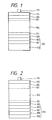
- Fig. 1 is a cross-sectional view illustrating a photovoltaic device according to an embodiment of the present invention.
- Fig. 2 is a cross-sectional view illustrating a photovoltaic device according to another embodiment of the present invention.
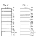
- Fig. 3 is a cross-sectional view illustrating a photovoltaic device according to still another embodiment of the present invention.
- Fig. 4 is a cross-sectional view illustrating a photovoltaic device according to further embodiment of the present invention.
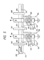
- Fig. 5 is a cross-sectional view illustrating an example of an apparatus having a plurality of chambers separated from each other for producing a reflecting layer.
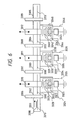
- Fig. 6 is a cross-sectional view illustrating another example of an apparatus having a plurality of chambers separated from each other for producing a reflecting layer.
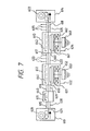
- Fig. 7 is a cross-sectional view illustrating an example of a roll-to-roll type apparatus for producing a reflecting layer.
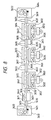
- Fig. 8 is a cross-sectional view illustrating another example of a roll-to-roll type apparatus for producing a reflecting layer.
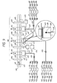
- Fig. 9 is a cross-sectional view illustrating an example of an apparatus having a plurality of chambers separated from each other for producing a photovoltaic device.
- Fig. 10 is a cross-sectional view illustrating an example of a roll-to-roll type apparatus for producing a photovoltaic device.
- the present invention provides a method for producing a photovoltaic device comprising a base member comprising a substrate and superposingly formed thereon a reflecting layer and a reflection enhancing layer, and a pin structure formed of an n-type, i-type and p-type semiconducor layers containing silicon atoms and being non-single crystal as crystal structure.
- the method of the invention can solve the problem of degradation which may occur when the photovoltaic device is used at a high temperature with high humidity.
- the method of the present invention is characterized that the method includes the steps of: (a) depositing a material constituting the reflecting layer, at a substrate temperature of from 200 to 500°C to form the reflecting layer; (b) lowering after the step (a) the substrate temperature to 100°C or below by means of a gas; and (c) depositing after the step (b) a material constituting the reflection enhancing layer, on the reflecting layer at a substrate temperature of from 200 to 400°C to form the reflection enhancing layer.
- a reflecting layer comprising, for example, a metal, having irregularities on its surface, which result in an improvement in confinement of light.
- the photovoltaic device of the present invention has the reflecting layer having high reflectivity.
- the present invention is applicable to a production method called a roll-to-roll method, semiconductor layers and other films are continuously formed on a long rolled substrate.
- a reflecting layer and a reflection enhancing layer are formed successively on the substrate in production of a device according to a roll-to-roll method, oxygen atoms diffuse toward the underlying reflecting layer maintained at a high temperature during the process of depositing a material for forming the reflection enhancing layer (a transparent conductive layer), for example an oxide.
- a transparent conductive layer for example an oxide.
- the reflecting layer is oxidized excessively.
- the above problem of the excessive oxidation can be avoided.
- the photovoltaic device produced according to the method of the present invention has improved resistance against external force which is imposed on the device for example when the photovoltaic device is bent. Therefore, a plurality of photovoltaic devices can be integrated into a single module without having a problem of the separation of a semiconductor layer from the substrate.
- the method of the present invention suppresses the oxidation of the surface of the reflecting layer composed of metal or the like. This results in an improvement in adhesion between the reflecting layer and the reflection enhancing layer of the photovoltaic device. Furthermore, according to the method of the present invention, it is possible to form a thin oxide film thereby reducing the strain. As a result, the stresses in the reflection layer and the reflection enhancing layer are reduced.
- the substrate is cooled in the subsequent step (b) at a cooling rate of 1 to 50°C/sec so as to minimize the thermal strain caused by the change in temperature during the process of cooling the substrate thereby preventing the upper layers from peeling from the substrate during the production process or in the completed photovoltaic device and also preventing the increase in the series resistance that is the sum of resistance of the whole layers constituting the photovoltaic device.
- step (c) of forming the reflection enhancing layer the temperature of the substrate is raised in a rate of 10 to 100°C/sec up to a temperature in the range from 200 to 400°C. This suppresses the thermal strain caused by the change in temperature which occurs when the temperature of the substrate is reduced after the step (c). The reduction in the thermal strain prevents the upper layers from peeling from the substrate and also prevents the increase in the series resistance of the photovoltaic device.
- the cooling of the substrate in step (b) is performed with gas.
- gas selected from the group consisting of hydrogen gas, helium gas, and argon gas are used to cool the substrate down to a desired temperature without introducing oxidation of the surface of the reflecting layer which has already been formed.
- Figs. 1 to 4 illustrate some examples of the structure of the photovoltaic device produced according to the method of the present invention.
- the photovoltaic device has one pin structure, while the photovoltaic device has three pin structures in the examples shown in Figs. 3 and 4.
- Fig. 1 is a cross-sectional view illustrating a photovoltaic device having one pin structure (a single type device).
- the photovoltaic device of this type can be constructed in two different ways. In the first structure, light is incident on the surface opposite to the base member, while light is incident on the surface of the base member in the second structure.
- the photovoltaic device includes: a base member 190 including a substrate 100, a reflecting layer 101 and a reflection enhancing layer 102; a first n-type layer (or p-type layer) 103; an n/i (or p/i) buffer layer 151; a first i-type layer 104; a p/i (or n/i) buffer layer 161; a first p-type layer (or n-type layer) 105; a transparent electrode 112; and a collector electrode 113, wherein these elements are formed one on another from the bottom to the top in the above-explained order.
- an intermediate layer (multifunction adhesive layer) 199 may be disposed between the substrate 100 and the reflecting layer 101 in the base member 190 as shown in Fig. 1 so as to improve the performance such as the adhesion between the substrate 100 and the reflecting layer 101.
- an intermediate layer (multifunction adhesive layer) 199 may be disposed between the substrate 100 and the reflecting layer 101 in the base member 190 as shown in Fig. 1 so as to improve the performance such as the adhesion between the substrate 100 and the reflecting layer 101.
- Fig. 3 is a cross-sectional view illustrating a photovoltaic device having three pin structures (a triple type device).
- the photovoltaic device of this type can also be constructed in two different ways. That is, in the first structure, light is incident on the surface opposite to the base member, while light is incident on the surface of the base member in the second structure.
- the photovoltaic device comprises: a base member 290 comprising a substrate 200, a reflecting layer 201 and a reflection enhancing layer 202; a first n-type layer (or p-type layer) 203; a first n/i (or p/i) buffer layer 251; a first i-type layer 204; a first p/i (or n/i) buffer layer 261; a first p-type layer (or n-type layer) 205; a second n-type layer (or p-type layer) 206; a second n/i (or p/i) buffer layer 252; a second i-type layer 207; a second p/i (or n/i) buffer layer 262; a second p-type layer (or n-type layer) 208; a third n-type layer (or p-type layer) 209;
- an. intermediate layer (multifunction adhesive layer) 299 may be disposed between the substrate 200 and the reflecting layer 201 in the base member 290 as shown in Fig. 4 so as to improve the performance such as the adhesion between the substrate 200 and the reflecting layer 201 (in Fig. 4, similar parts to those in Fig. 3 are denoted by similar reference numerals).
- the annealing is performed in an ambient of hydrogen gas, helium gas or argon gas.
- Figs. 5 to 8 illustrates some examples of apparatus which can be used to form a reflecting layer and a reflection enhancing layer according to the present invention.
- the apparatus has a plurality of chambers separated from each other.
- the apparatus is of the roll-to-roll type.
- the apparatus shown in Fig. 5 or 6 is of the type in which layer formation is performed from wafer to wafer.
- a substrate having a predetermined shape is successively carried from a chamber to another of the plurality of chambers, and different layers are formed on the substrate in different chambers.
- the apparatus 300 having the structure shown in Fig. 5 includes: a load-lock chamber 301; transfer chambers 302 and 303; an unload chamber 304; gate valves 306, 307, and 308; substrate heaters 310 and 311; a substrate transfer rail 313; a light reflecting layer deposition chamber 320; a reflection enhancing layer deposition chamber 330; targets 321 and 331; target electrodes 322 and 332; gas inlet pipes 324 and 334; sputtering power supplies 325 and 335; and target shutters 326 and 336.
- a source gas supplying system (not shown) is connected to the apparatus shown in Fig. 5 via the gas inlet pipes.
- the source gas supplying system includes gas cylinders containing ultra-high-purity hydrogen, argon, and helium, respectively.
- On the target 321 a material such as metal to be used to form a reflecting layer is placed.
- On the target 331 a material such as an oxide to be used to form a reflection enhancing layer is placed.
- a substrate 390 is transferred from chamber to chamber in the apparatus in the direction denoted by the arrow wherein a layer is deposited on the substrate 390 in a chamber and then another layer is further deposited thereon in the other chamber.
- the substrate 390 is cleaned with acetone and isopropanol or the like by means of ultrasonic cleaning, and then dried with hot air.
- the substrate 390 is placed such that the back surface thereof comes into contact with the substrate heater 310 so that the substrate 390 is heated at a rate of 10 to 100°C/sec up to a temperature in the range from 200 to 500°C.
- the inside of the deposition chamber 320 is evacuated with the vacuum pump (not shown) down to a pressure of for example about 3 ⁇ 10 -6 Torr.
- SA-4 For example argon gas is introduced into the chamber 320 via the gas inlet pipe 324 at a desired flow rate.
- the pressure inside the deposition chamber 320 is adjusted to for example 1 to 30 mTorr by means of a conductance valve (not shown).
- An electric current is passed through a toroidal coil 323 and for example DC power of for example 100 V to 1000 V is supplied to the target from the sputtering power supply 325 thereby generating an argon plasma.
- a target shutter 326 is opened so as to start depositing a metal material on the surface of the substrate thereby forming a light reflecting layer (101 in the case of the device shown in Fig. 1 or 201 in the case of the device shown in Fig. 3) having a thickness of 0.25 ⁇ m to 1 ⁇ m. After completion of the deposition, the target shutter 326 is closed and the plasma is turned off.
- the substrate heater 310 is raised to an upper position. Then in the ambient of He gas serving as the substrate cooling gas, the substrate is cooled preferably at a rate of 1 to 50°C/sec down to a temperature equal to or lower than 100°C.
- the gate valve 307 is then opened, and the substrate 390 is transferred into the deposition chamber 330 via the transfer chamber 303 wherein both the deposition chamber 330 and the transfer chamber 303 have already been evacuated with a vacuum pump (not shown).
- the substrate 390 is placed such that the back surface thereof comes into contact with the substrate heater 311 so that the substrate 390 is heated preferably at a rate of 10 to 100°C/sec up to a temperature in the range from 200 to 400°C.
- the inside of the deposition chamber 330 is evacuated with the vacuum pump (not shown) down to a pressure of for example about 2 ⁇ 10 -6 Torr.
- a target shutter 336 is opened so as to start depositing a metal material on the surface of the substrate thereby forming a reflection enhancing layer (102 in the case of the device shown in Fig. 1 or 202 in the case of the device shown in Fig. 3) having a thickness of 0.05 ⁇ m to 4 ⁇ m. After completion of the deposition, the target shutter 336 is closed and the plasma is turned off.
- the substrate heater 311 is raised to an upper position. Then in the ambient of He gas serving as the substrate cooling gas, the substrate is cooled preferably at a rate of 1 to 50°C/sec down to a temperature equal to or lower than 100°C.
- the gate valve 308 is then opened, and the substrate 390 is transferred into the unload chamber 304 which has already been evacuated with a vacuum pump (not shown). Thus, the reflecting layer and the reflection enhancing layer are formed.
- the apparatus having the plurality of separated chambers shown in Fig. 6 can be used to successively form an intermediate layer, a reflecting layer and a reflection enhancing layer on a substrate.
- the apparatus 3300 shown in Fig. 6 includes: a load-lock chamber 3301; transfer chambers 3302, 3303 and 3304; an unload chamber 3305; gate valves 3306, 3307, 3308 and 3309; substrate heaters 3310, 3311 and 3312; a substrate transfer rail 3313; an intermediate layer deposition chamber 3320; a light reflecting layer deposition chamber 3330; a reflection enhancing layer deposition chamber 3340; targets 3321, 3331 and 3341; target electrodes 3322, 3332 and 3342; gas inlet pipes 3324, 3334 and 3344; sputtering electrodes 3325, 3335 and 3345; and target shutters 3326, 3336 and 3346.
- a source gas supplying system (not shown) is connected to the apparatus shown in Fig. 6 via the gas inlet pipes.
- the source gas supplying system includes gas cylinders containing ultra-high-purity hydrogen, argon, and helium, respectively.
- On the target 321 a material to be used to form an intermediate layer is placed.
- On the target 331 a material such as metal to be used to form a reflecting layer is placed.
- a substrate 3390 is transferred from chamber to chamber in the apparatus in the direction denoted by the arrow wherein a layer is deposited on the substrate 3390 in one chamber and another layer is further deposited thereon in another chamber, and so on.
- the substrate is cleaned with acetone and isopropanol or the like by means of ultrasonic cleaning, and then dried with hot air.
- the cleaned substrate 3390 is placed on the substrate transfer rail 3313 in the load chamber 3301, and the load chamber 3301 is evacuated with a vacuum pump (not shown) down to a pressure of for example about 1 ⁇ 10 -5 Torr.
- the substrate 3390 is placed such that the back surface thereof comes into contact with the substrate heater 3310 so that the substrate 3390 is heated preferably up to a temperature in the range from 30 to 500°C.
- the inside of the deposition chamber 3320 is evacuated with the vacuum pump (not shown) down to a pressure of for example about 2 ⁇ 10 -6 Torr.
- argon gas is introduced into the chamber 3320 via the gas inlet pipe 3324 at a desired flow rate.
- the pressure inside the deposition chamber 3320 is adjusted to for example 1 to 30 mTorr by means of a conductance valve (not shown).
- An electric current is passed through a toroidal coil 3323 and for example DC power of for example 100 V to 1000 V is supplied to the target from the sputtering power supply 3325 thereby generating an argon plasma.
- a target shutter 3326 is opened so as to start depositing an intermediate layer (199 in the case of the device shown in Fig. 2 or 299 in the case of the device shown in Fig. 4) on the surface of the substrate.
- the target shutter 3326 is closed and the plasma is turned off.
- the gate valve 3307 is then opened and the substrate 3390 is transferred into the deposition chamber 3330.
- the substrate 3390 is placed such that the back surface thereof comes into contact with the substrate heater 3311 so that the substrate 3390 is heated preferably at a rate of 10 to 100°C/sec up to a temperature in the range from 200 to 500°C.
- the inside of the deposition chamber 3330 is evacuated with the vacuum pump (not shown) down to a pressure of for example about 3 ⁇ 10 -6 Torr.
- argon gas is introduced into the chamber 3330 via the gas inlet pipe 3334 at a desired flow rate.
- the pressure inside the deposition chamber 3330 is adjusted to for example 1 to 30 mTorr by means of a conductance valve (not shown).
- An electric current is passed through a toroidal coil 3333 and for example DC power of for example 100 V to 1000 V is supplied to the target from the sputtering power supply 3335 thereby generating an argon plasma.
- a target shutter 3336 is opened so as to start depositing a metal material thereby forming a reflecting layer (101 in the case of the device shown in Fig. 2 or 201 in the case of the device shown in Fig. 4) on the surface of the substrate.
- a desired value in the range from 0.25 ⁇ m to 1 ⁇ m, the target shutter 3336 is closed and the plasma is turned off.
- the substrate heater 3311 is raised to an upper position. Then in the ambient of He gas serving as the substrate cooling gas, the substrate is cooled preferably at a rate of 1 to 50°C/sec down to a temperature equal to or lower than 100°C.
- the gate valve 3308 is then opened, and the substrate 3390 is transferred into the deposition chamber 3340 via the transfer chamber 3304 wherein both the deposition chamber 3340 and the transfer chamber 3304 have already been evacuated with a vacuum pump (not shown).
- the substrate 3390 is placed such that the back surface thereof comes into contact with the substrate heater 3312 so that the substrate 3390 is heated preferably at a rate of 10 to 100°C/sec up to a temperature in the range from 200 to 400°C.
- the inside of the deposition chamber 3340 is evacuated with the vacuum pump (not shown) down to a pressure of for example about 2 ⁇ 10 -6 Torr.
- argon gas is introduced into the chamber 3340 via the gas inlet pipe 3334 at a desired flow rate.
- the pressure inside the deposition chamber 3340 is adjusted to for example 1 to 30 mTorr by means of a conductance valve (not shown).
- An electric current is passed through a toroidal coil 3343 and for example DC power of for example 100 V to 1000 V is supplied to the target from the sputtering power supply 3345 thereby generating an argon plasma.
- a target shutter 3346 is opened so as to start depositing a reflection enhancing layer (102 in the case of the device shown in Fig. 2 or 202 in the case of the device shown in Fig. 4) on the surface of Ag reflecting layer 101.
- a reflection enhancing layer 102 in the case of the device shown in Fig. 2 or 202 in the case of the device shown in Fig. 4 ⁇ m.
- the substrate heater 3312 is raised to an upper position. Then in the ambient of He gas serving as the substrate cooling gas, the substrate is cooled preferably at a rate of 1 to 50°C/sec down to a temperature equal to or lower than 100°C.
- the gate valve 3309 is then opened, and the substrate 3390 is transferred into the unload chamber 3305 which has already been evacuated with a vacuum pump (not shown).
- a vacuum pump not shown.
- a rolled ribbon-shaped substrate is passed through a plurality of chambers so that a plurality of layers are successively formed on the substrate.
- the apparatus 600 shown in Fig. 7 includes: a substrate feeding chamber 610; a plurality of deposition chambers 611-613; and a substrate winding chamber 614. These chambers are arranged side by side, and adjacent chambers are connected to each other via separation paths 615, 616, 617, and 618. Each chamber has a vent via which the inside of the chamber can be evacuated.
- the ribbon-shaped substrate 621 is moved in the apparatus in the direction denoted by the arrow so that layers are deposited on the substrate from chamber to chamber.
- the ribbon-shaped substrate 621 is fed into the apparatus and is passed through the respective deposition chambers and separation paths.
- the ribbon-shaped substrate 621 is then wound into a roll in the substrate winding chamber. Gas is introduced into each separation path via a gas inlet, and the gas is exhausted from the chamber via the vent so that layers are deposited one on another during the passage of the ribbon-shaped substrate 621.
- a light reflecting layer is formed in the deposition chamber 612, and a reflection enhancing layer (102 in the case of the structure shown in Fig. 1 and 202 in the case of the structure shown in Fig. 3) is formed in the deposition chamber 613.
- each deposition chamber there is provided a halogen lamp heater 640, 641, and 642 for heating the substrate from the back thereof up to a temperature predetermined for each chamber.
- Each separation path 617, 618 has a cooling mechanism.
- a film is deposited for example by means of the DC magnetron sputtering technique in the ambient of for example Ar gas introduced via a gas inlet 632.
- a material such as metal for forming the reflecting layer is employed as the target 650.
- a film is deposited for example by means of the DC or RF magnetron sputtering technique in the ambient of for example Ar gas introduced via a gas inlet 634.
- a material such as an oxide for forming the reflection enhancing layer is employed as the target 660.
- the ribbon-shaped substrate 621 is wound into a roll in the substrate winding chamber 614.
- the apparatus of the roll-to-roll type shown in Fig. 8 can be employed to form an intermediate layer, a reflecting layer, and a reflection enhancing layer on a substrate in the production of a photovoltaic device such as that shown in Fig. 2 or 4.
- the apparatus 3600 shown in Fig. 8 includes: a substrate feeding chamber 3610; a plurality of deposition chambers 3611-3613; and a substrate winding chamber 3684. These chambers are arranged side by side, and adjacent chambers are connected to each other via separation paths 3615, 3616, 3617, 3618, and 3619. Each chamber has a vent via which the inside of the chamber can be evacuated.
- the ribbon-shaped substrate 3621 is moved in the apparatus in the direction denoted by the arrow so that layers are deposited on the substrate from chamber to chamber.
- the ribbon-shaped substrate 3621 is fed into the apparatus and is passed through the respective deposition chambers and separation paths.
- the ribbon-shaped substrate 3621 is then wound into a roll in the substrate winding chamber. Gas is introduced into each separation path via a gas inlet, and the gas is exhausted from the chamber via the vent so that layers are deposited one on another during the passage of the ribbon-shaped substrate 3621.
- an intermediate layer (199 in the case of the structure shown in Fig. 2 and 299 in the case of the structure shown in Fig. 4) is formed.
- a reflecting layer (101 in the case of the structure shown in Fig. 2 and 201 in the case of the structure shown in Fig. 4) is formed.
- a reflection enhancing layer (102 in the case of the structure shown in Fig. 2 and 204 in the case of the structure shown in Fig. 4) is formed in the deposition chamber 3614.
- each deposition chamber there is provided a halogen lamp heater 3640, 3641, 3642, 3643 for heating the substrate from the back thereof up to a temperature predetermined for each chamber.
- Each separation path 3617, 3618, 3619 has a cooling mechanism.
- a film is deposited for example by means of the DC magnetron sputtering technique in the ambient of for example Ar gas introduced via a gas inlet 3632.
- a material for forming the intermediate layer is employed as the target 3650.
- a film is deposited for example by means of the DC or RF magnetron sputtering technique in the ambient of for example Ar gas introduced via a gas inlet 3634.
- a material for forming the reflecting layer is employed as the target 3660.
- a film is deposited for example by means of the DC magnetron sputtering technique in for example Ar gas ambient introduced via a gas inlet 3636.
- a material for forming the reflection enhancing layer is employed as the target 3670.
- the ribbon-shaped substrate 3621 is wound into a roll in the substrate winding chamber 3614.
- the apparatus shown in Fig. 9 or 10 can be used.
- the apparatus shown in Fig. 9 is of the type having a plurality of separated chambers, and the apparatus shown in Fig. 10 is of the roll-to-roll type.
- substrates having a predetermined shape are fed successively into the plurality of chambers, and the deposition of a semiconductor layer is performed in each chamber from one substrate to another thereby producing a device having any of structures shown in Figs. 1-4.
- the apparatus 400 of Fig. 9 includes: a load chamber 401; transfer chambers 402, 403, 404; unload chambers 405; gate valves 406, 407, 408, 409; substrate heaters 410, 411, 412; a substrate transfer rail 413; an n-type layer (or p-type layer) deposition chamber 417; an i-type layer deposition chamber 418; a p-type layer (or n-type layer) deposition chamber 419; a plasma excitation cups 420, 421; power supplies 422, 423, 424; a microwave entrance window 425; a wave guide 426; gas inlet pipes 429, 449, 469; valves 430, 431, 432, 433, 434, 441, 442, 443, 444, 450, 451, 452, 453, 454, 455, 461, 462, 463, 464, 465, 470, 471, 472, 474, 481, 482, 483, 484; mass flow controllers 436, 437, 438, 439
- All chambers of the deposition apparatus 400 are evacuated down to a pressure of for example 10 -6 Torr or lower via turbo-molecular pumps (not shown) connected to the respective chambers.
- the substrate holder 490 is put into the load chamber 401 and the door of the load chamber 401 is closed.
- the load chamber 401 is then pumped down to a predetermined pressure using an evacuation system (not shown) including a mechanical booster pump and a rotary pump (MP/RP evacuation system).
- the substrate heater 410 in the transfer chamber 402 is raised to an upper position so that the substrate holder 490 does not collide with the substrate heater 410.
- the substrate holder 490 is positioned so that the substrate comes to a location just below the heater 410.
- the substrate heater 410 is then lowered and the substrate is moved into the n-layer deposition chamber.
- the temperature of the substrate is adjusted to a value suitable for the deposition of the n-type layer.
- a gas containing silicon such as SiH 4 , Si 2 H 6 or the like and a gas containing a Group V element to be used to form the n-type layer are introduced into the deposition chamber 417 via the valve 433, the mass flow controller 438, and the valve 433.
- hydrogen gas is also introduced into the deposition chamber 417 at a proper flow rate depending on the characteristics of the n-type layer to be deposited.
- the source gases for depositing the n-type layer are introduced into the deposition chamber 417 and the vent valve (not shown) is adjusted so that the pressure inside the deposition chamber 417 has a proper value for example in the range from 0.1 Torr to 10 Torr.
- the RF power is then applied from the RF power supply 422 to the plasma excitation cup 420 thereby generating plasma discharging, which is maintained for a proper time duration until the n-type layer having a desired thickness has been deposited.
- the gate valve 407 is opened, and the substrate holder 490 is moved into the transfer chamber 403. The gate valve 407 is then closed.
- the position of the substrate holder 490 is then adjusted so that the substrate can be heated by the substrate heater 411.
- the substrate heater 411 is moved such that it comes into contact with the substrate and the substrate is heated up to a proper temperature.
- Hydrogen gas or an inert gas such as helium is introduced into the deposition chamber 418.
- the deposition chamber 418 is preferable maintained at a pressure equal to that at which an n/i buffer layer will be deposited in the following step.
- the gas for use during the heating of the substrate is shut off, and source gases to be used to deposit the n/i buffer layer are supplied into the deposition chamber 418 from the source gas supplying system.
- the valves 462, 463, and 464 are opened and the flow rates of hydrogen gas, silane gas, and germane gas are adjusted to desired values by the mass flow controllers 457, 458, and 459.
- the valves 452, 453, 454, and 450 are then opened so as to introduce the above gases into the deposition chamber 418.
- These source gases are pumped by a diffusion pump (not shown) so that the inside of the deposition chamber 418 is maintained at a proper pressure.
- RF power is applied to the bias bar from the RF power supply (not shown) and an n/i buffer layer is deposited by means of RF plasma CVD.
- the n/i buffer layer is deposited at a deposition rate smaller than that at which an i-type layer will be deposited on it in the following step.
- the substrate is then heated to a temperature suitable for depositing the i-type layer.
- hydrogen gas or an inert gas such as helium is preferably introduced into the deposition chamber 418 via the valves 461, 451, and 450 wherein the flow rate of the gas is controlled by a mass flow controller.
- the deposition chamber 418 is preferable maintained at a pressure equal to that at which the i-type layer will be deposited.
- the gas for use during the heating of the substrate is shut off, and source gases to be used to deposit the i-type layer are supplied into the deposition chamber 418 from the source gas supplying system.
- the valves 462, 463, and 464 are opened and the flow rates of hydrogen gas, silane gas, and germane gas are adjusted to desired values by the mass flow controllers 457, 458, and 459.
- the valves 452, 453, 454, and 450 are then opened so as to introduce the above gases into the deposition chamber 418.
- these source gases are pumped by the diffusion pump (not shown) so that the inside of the deposition chamber 418 is maintained at a proper pressure.
- microwave power is introduced via the wave guide 426 and the microwave entrance window 425 into the deposition chamber 418.
- DC bias power may also be introduced via the bias bar into the deposition chamber 418 from an external DC power supply, RF power supply, or VHF power supply 424, as shown in an enlarged fashion in Figure 9.
- the i-type layer having a desired thickness is deposited.
- the microwave power and the bias power are turned off.
- the inside of the deposition chamber 418 is purged with hydrogen gas or an inert gas such as helium gas as required.
- a p/i buffer layer having a desired thickness is then deposited on the i-type layer in a similar manner to that in the n/i buffer layer.
- the inside of the deposition chamber 418 is purged with hydrogen gas or an inert gas such as helium gas as required.
- the evacuating system is switched from the diffusion pump to the turbo-molecular pump and the deposition chamber is pumped down to a pressure for example 10 -6 Torr or less.
- the substrate heater is raised so that the substrate holder may move without collision with the heater.
- the gate valve 408 is opened, and the substrate holder is moved to the transfer chamber 404 via the transfer chamber 403. The gate valve 408 is then closed.
- the substrate holder is moved to a position just below the substrate heater 412, and the substrate is heated by the substrate heater 412.
- the evacuating systems be switched from the turbo-molecular pump to the MP/RP and hydrogen gas or an inert gas such as helium be supplied into the deposition chamber while maintaining the pressure inside the deposition chamber at a value equal to that at which a p-type layer will be deposited.
- the hydrogen gas or inert gas for use during the heating of the substrate is shut off, and source gases-such as H 2 , SiH 4 , and a gas containing, for the case of the deposition of a p-type layer, Group III element for example BF 3 are supplied into the deposition chamber 419 via the valves 482, 483, 484, the mass flow controllers 477, 478, 479, the valves 472, 473, 474, and the gas inlet 469.
- the vent valve is adjusted so that the pressure inside the deposition chamber 419 is maintained at a proper value.
- RF power is supplied to the plasma excitation cup from the RF power supply 423.
- deposition is performed for a proper time duration thereby forming a p-type layer.
- the RF power and the source gases are stopped, and the inside of the deposition chamber is purged with hydrogen gas or an inert gas such as helium gas.
- the evacuating system is switched from the MP/RP to the turbo-molecular pump and the deposition chamber is pumped down to a pressure 10 -6 Torr or less. Meanwhile, the substrate heater is raised. Furthermore, the gate valve 409 is opened and the substrate holder 490 is moved to the unload chamber 405. The gate valve 409 is then closed. If the substrate holder has been cooled down to a temperature 100°C or less, the door of the unload chamber is opened and the substrate is taken out to the outside. In this way, semiconductor layers in the form of a pin structure have been formed on the substrate.
- the substrate on which the pin semiconductor layers have been formed is then placed in a vacuum vapor deposition chamber and a transparent electrode is vapor-deposited onto the top of the semiconductor layers.
- the substrate on which the transparent electrode has been formed in the previous step is then placed in another vacuum vapor deposition chamber and a collector electrode is vapor-deposited onto the transparent electrode.
- a rolled ribbon-shaped substrate is passed through a plurality of chambers connected to each other so that a plurality of semiconductor layers are successively formed on the substrate or required processing is performed thereby producing a device having any of structures shown in Figs. 1 to 4.
- the deposition apparatus 5000 includes thirteen chambers connected to each other. These thirteen chambers are disposed between a load chamber 5010 from which a substrate in the sheet form is fed into the chambers and an unload chamber 5150.
- the thirteen chambers are: a first n-type layer deposition chamber 5020; a first RF i-layer (n/i) deposition chamber 5030; a first MW (microwave) i-layer deposition chamber 5040; a first RF i-layer (p/i) deposition chamber 5050; a first p-type layer deposition chamber 5060; a second n-type layer deposition chamber 5070; a second RF i-layer (n/i) deposition chamber 5080; a second MW i-layer deposition chamber 5090; a second RF i-layer (p/i) deposition chamber 5100; a second p-type layer deposition chamber 5110; a second RF i-layer deposition chamber 5130; and a third p-type layer
- the adjacent chambers are connected to each other via a gas gate (5201, 5202, 5203, 5204, 5205, 5206, 5207, 5208, 5209, 5210, 5211, 5212, 5213, 5214).
- Each gas gate has a gas supply pipe (5301, 5302, 5303, 5304, 5305, 5306, 5307, 5308, 5309, 5310, 5311, 5312, 5313, 5314) via which gas is supplied into the gas gate.
- the load chamber 5010, the unload chamber 5150, and the deposition chambers are each connected to an evacuation pump (5012, 5022, 5032, 5042, 5052, 5062, 5072, 5082, 5092, 5102, 5112, 5122, 5132, 5142, 5152) via an exhaust pipe (5011, 5021, 5031, 5041, 5051, 5061, 5071, 5081, 5091, 5101, 5111, 5121, 5131, 5141, 5151).
- an evacuation pump (5012, 5022, 5032, 5042, 5052, 5062, 5072, 5082, 5092, 5102, 5112, 5122, 5132, 5142, 5152) via an exhaust pipe (5011, 5021, 5031, 5041, 5051, 5061, 5071, 5081, 5091, 5101, 5111, 5121, 5131, 5141, 5151).
- a source gas supply pipe (5025, 5035, 5045, 5055, 5065, 5075, 5085, 5095, 5105, 5115, 5125, 5135, 5145) is connected to each deposition chamber wherein the other end of each source gas supply pipe is connected to a mixing device (5026, 5036, 5046, 5056, 5066, 5076, 5086, 5096, 5106, 5116, 5126, 5136, 5146).
- each deposition chamber is connected to a high frequency (RF) power supply (5024, 5034, 5044, 5054, 5064, 5074, 5084, 5094, 5104, 5114, 5124, 5134, 5144) via an RF coaxial cable (5023, 5033, 5043, 5053, 5063, 5073, 5083, 5093, 5103, 5113, 5123, 5133, 5143).
- RF radio frequency
- a sheet feeding mechanism 5400 is disposed in the load chamber 5010, and a sheet winding mechanism is disposed in the unload chamber 5150.
- a substrate in the form of a sheet 5401 is fed from the sheet feeding mechanism 5400 and is passed through the above-explained thirteen deposition chambers. The substrate 5401 is then wound by the sheet winding mechanism 5402.
- the MW i-layer deposition chamber is also connected to a bias power supply via a coaxial cable. Furthermore, the MW i-layer deposition chamber is connected to an exhaust gas disposal system.
- (R-3) Hydrogen gas is supplied from the gate gas supplying system to the respective gas gates 5201, 5202, 5203, 5204, 5205, 5206, 5207, 5208, 5209, 5210, 5211, 5212, 5213, and 5214.
- the flow rates of the hydrogen gas supplied to the gas gates are controlled so that the source gases are not mixed between adjacent deposition chambers.
- the preferable flow rates depend on the intervals of the sheet-shaped substrate passing through the gas gates. In the case where the intervals are 0.5 to 5 mm, it is preferable to set the flow rates of the hydrogen gas to a value in the range from 200 sccm to 3000 sccm.
- the sheet-shaped substrate 5401 is heated to a predetermined substrate temperature by a substrate heater provided in each deposition chamber. If the substrate temperature has become stable, the hydrogen gas supplied to each deposition chamber is switched to proper source gas depending on the respective deposition chambers. After switching the gas to the source gas, the degree of opening of the exhaust valve of each evacuation system is adjusted so that the inside of each deposition chamber is maintained at a proper gas pressure.
- the load chamber 5010 is closed, and is evacuated to a predetermined pressure.
- the pinch valve is opened, and plasma discharging is started again so as to form a photovoltaic device on the substrate.
- the feeding of the sheet-shaped substrate is started. The above processing steps are performed repeatedly until the photovoltaic device having a structure such as that shown in Fig. 3 or 4 has been formed on the roll of the sheet-shaped substrate.
- the material of the substrate used in the present invention should have proper mechanical strength and electrical conductivity, and should not have excessive deformation or strain when it is heated to a temperature required for the film deposition. Furthermore, it is also desirable that no degradation occur in the adhesion between the substrate and the reflecting layer or the reflection enhancing layer due to the hydrogen plasma treatment which is performed after depositing the reflecting layer and the reflection enhancing layer.
- examples of preferable substrate materials include: a thin film made up of a metallic material such as stainless steel, aluminum, aluminum alloys, iron, iron alloys, copper, copper alloys, etc.; a combination of these metallic materials; any one of the above-explained materials coated with a different thin metal film and/or an insulating thin film such as SiO 2 , Si 3 N 4 , Al 2 O 3 , AlN wherein the coating may be performed by means of sputtering, vapor deposition, or plating; a sheet of heat-resisting resin such as polyimide, polyamide, polyethylene terephthalate, and epoxy resin; and a combination of any of the above sheet of heat-resisting resin and a fiber material such as glass fiber, carbon fiber, boron fiber, and metal fiber wherein the surface of the material is coated, by means of sputtering, vapor deposition, or plating, with a conductive thin film such as metal elements, metal alloys, or transparent and conductive oxides.
- the thickness of the substrate is preferably as thin as possible to achieve low cost and small volume in the range that can provides a sufficient mechanical strength such that it is not easily broken when it is bent during the film deposition process or during the transferring process of the substrate. More specifically, the thickness of the substrate is preferably in the range from 0.01 mm to 5 mm, more preferably, from 0.02 mm to 2 mm, and most preferably, from 0.05 mm to 1 mm. In particular, a thin metallic film is preferable because a very thin film can be obtained while maintaining a sufficient mechanical strength.
- width of the substrate there is no special limitation regarding the width of the substrate and the width may be properly selected depending on the size of the vacuum chamber or other factors.
- a long substrate in a rolled form or a plurality of long substrates connected by means of welding into a longer form may be employed.
- the substrate is heated and cooled for a short time duration, and thus it is preferable that heat conduction in a direction along the transfer motion of the substrate should be as small as possible. On the other hand, it is desirable that great heat conduction occur in the direction of the thickness of the substrate so that the surface of the substrate can be quickly heated and cooled.
- One simple way to have great heat conduction in the thickness direction and small heat conduction in the movement direction is to employ a thin substrate. If it is assumed that the substrate has an uniform thickness, it is preferable the product of the thermal conductivity and the thickness be 1 ⁇ 10 -1 W/K or less, and more preferably 0.5 ⁇ 10 -2 W/K or less.
- Examples of materials suitable for the reflecting layer include metals such as Ag, Au, Pt, Ni, Cr, Cu, Al, Ti, Zn, Mo, and W, and alloys of these metals, wherein the reflecting layer may be formed of any of these materials into a thin film shape by means of vapor deposition, electron beam vapor deposition, or sputtering.
- the thin metal film should be formed such that the film does not act as a significant series resistance of a photovoltaic semiconductor device.
- the sheet resistance of the reflecting layer should preferably be 50 ⁇ or less, and more preferably, 10 ⁇ or less.
- materials containing Ag or Al-Si alloy as a main constituent are suitable as the material of the reflecting layer. If such a material is employed, the resultant reflecting layer has irregularities on its surface, which result in an improvement in confinement of light.
- the Si content in the alloy be in the range from 5 to 20%.
- the reflection enhancing layer (substantially, a transparent conductive layer) allows the semiconductor layers to absorb a greater amount of incident light such as solar radiation or radiation of a daylight fluorescent lamp.
- the transmittance of the reflection enhancing layer be 85% or more.
- the sheet resistance of the reflection enhancing layer be 100 ⁇ or less so that it does not act as a significant series resistance of a photovoltaic device.
- materials suitable for this purpose are metal oxides such as SnO 2 , In 2 O 3 , ZnO, CdO, Cd 2 SnO 4 , ITO (In 2 O 3 + SnO 2 ), etc. Of these materials, ZnO is particularly suitable to form a reflection enhancing layer having discontinuous surface with high-reflectivity uneveness on its surface.
- the layer contain metal element such as Ag, Ni, Fe, Cr, or Cu.
- the content of such metal in the reflection enhancing layer is preferably in the range from 10 to 10000 ppm. If the metal content is less than 10 ppm, the metal does not have any effects. On the other hand, if the metal content is greater than 10000 ppm, the adhesion of the reflection enhancing layer to the semiconductor layer becomes poor. Thus, the addition of a proper amount of metal results in an improvement in the adhesion of the reflection enhancing layer to the upper semiconductor layer and also results in a reduction in the whole device and series resistance of the device.
- the reflection enhancing layer have a thickness which results in an increase in reflectivity.
- Various techniques may be employed to form the reflection enhancing layer. They include resistive heating vapor deposition, electron beam vapor deposition, sputtering, and spraying techniques.
- the reflection enhancing layer may also be formed by mean of reactive sputtering using a target containing metal which is a constituent element of the above-explained oxide.
- an intermediate layer may be provided between the substrate and the reflecting layer so as to improve the adhesion between the substrate and the reflecting layer.
- the intermediate layer has a thickness in the range between 1 to 100 nm, although the optimum thickness depends on the material employed.
- the intermediate layer is suitable to form the intermediate layer.
- zinc oxide is particularly suitable to greatly improve the adhesion between the substrate and the reflecting layer.
- the intermediate layer of zinc oxide has a grain size 100 nm or less. If the grain size is greater than 100 nm, the adhesion becomes poor.
- the layer be formed at a deposition rate in the range from 0.1 to 20 nm/sec.
- the surface of the metal substrate is covered with an oxide. Therefore, if an oxide is employed as the intermediate layer, the intermediate layer exhibits good adhesion to the substrate. In this sense, zinc oxide is an excellent material.
- the oxygen content in the zinc oxide intermediate layer decrease with the position from the interface with the substrate to the interface with the reflecting layer.
- the zinc oxide intermediate layer contain metal element such as Ag, Ni, Fe, Cr, or Cu.
- the content of such metal in the intermediate layer is preferably in the range from 10 to 10000 ppm so as to obtain good adhesion between the substrate and the reflecting layer and so as to achieve a reduction in the series resistance of the device. If the metal content is 10 ppm or less, the metal does not have enough effects. On the other hand, if the metal content is greater than 10000 ppm, the adhesion becomes poor. Furthermore, it is desirable that metal be distributed in the intermediate layer in such a manner that the concentration of metal is higher near the substrate than the opposite side.
- Al-Si alloy is also suitable as the material of the intermediate layer.
- the intermediate layer of Al-Si alloy results in a great improvement in the adhesion between the reflecting layer and the substrate.
- the intermediate layer of Al-Si alloy has a grain size 100 nm or less. If the grain size is greater than 100 nm, the adhesion becomes poor.
- the intermediate layer is formed of Al-Si alloy, it is preferable that the layer be formed at a deposition rate in the range from 0.1 to 20 nm/sec.
- the substrate is preferably maintained at a temperate in the range 30 to 500°C.
- the intermediate layer formed under the above conditions leads to an improvement in adhesion between the lower layer or the substrate and the upper layer or the reflecting layer. Furthermore, the intermediate layer results in a reduction in series resistance of the completed device.
- the intermediate layer is deposited at a higher temperature. It is more preferable that the temperature of the substrate is gradually lowered after starting the deposition of the intermediate layer during the deposition process.
- the i-type semiconductor layer in the pin structure plays an important role in carrier generation in response to light illumination and also in transportation of generated carries.
- the i-type semiconductor layer is particularly important in photovoltaic devices made of an amorphous semiconductor material containing IV-group element or an alloy of IV-group element.
- the term "i-type layer" is used to describe not only semiconductor layers of the i-type but also those slightly exhibiting p- or n-type characteristics.
- the slightly p-type or n-type semiconductor layer serving as the i-type layer may be formed by incorporating hydrogen atoms (H, D) or halogen atoms (X) into an amorphous semiconductor material. As explained in further detail later, the incorporated atoms play important roles.
- Dangling bonds in the i-type layer are compensated by hydrogen (H, D) atoms or halogen (X) atoms included in the i-type layer.
- H, D hydrogen
- X halogen
- the interface states present at the interface between a p-type layer and an i-type layer, or between an n-type layer and an i-type layer are also compensated by hydrogen or halogen atoms, and thus the photoelectromotive force and photocurrent of a photovoltaic device are increased and the optical response characteristics are improved.
- the concentration of hydrogen atoms and/or halogen atoms included in the i-type layer is preferably in the range from 1 to 40 atomic %.
- the hydrogen atoms and/or halogen atoms are preferably distributed such that their concentration is greater near the interface between the p-type layer and the i-type layer or the interface between the n-type layer and the i-type layer than in the bulk region. More specifically, the above concentration is preferably in the range from 1.1 to 2 times the concentration in the bulk region.
- the concentration of hydrogen atoms and/or halogen atoms preferably changes in correspondence with the concentration of silicon atoms.
- the pin structures are preferably formed such that the i-type layer nearest to the light incidence side has the greatest bandgap and the bandgap decreases with the position of the i-type layer relative to the incidence side.
- An i-type layer having a wider bandgap can be formed of amorphous silicon or amorphous silicon carbide.
- An i-type layer having a narrower bandgap can be obtained by employing amorphous silicon germanium.
- amorphous silicon and amorphous silicon germanium are a-Si:H, a-Si:F, a-Si:H:F, a-SiGe:H, a-SiGe:F, a-SiGe:H:F wherein H and F are compensation elements for dangling bonds.
- the concentration of germanium is preferably changed in the thickness direction of the i-type layer. In particular, it is preferable that the concentration of germanium decrease continuously toward the n-type and/or p-type layer.
- the profile of the germanium concentration in the layers can be varied by controlling the ratio of the flow rate of a gas containing germanium to that of the total flow rate of source gases.
- the germanium concentration in the i-type layer can also be varied by varying the flow rate of hydrogen gas acting as a carrier gas of source gases in addition to the above-explained method in which the flow rate of a gas containing germanium is varied. For example, if the flow rate of hydrogen gas acting as the carrier gas is increased, then the concentration of germanium in a deposited layer (i-type layer) will be increased.
- the i-type layer in the pin structure is preferably formed of hydrogenated amorphous silicon (a-Si:H) having an optical bandgap (Eg) in the range from 1.60 eV to 1.85 eV, hydrogen concentration in the range from 1.0% to 25.0%, photoconductivity ( ⁇ p) of 1.0 ⁇ 10 -5 S/cm or more under the quasi-solar illumination condition of AM1.5 (100 mW/cm 2 ), dark conductivity ( ⁇ d) of 1.0 ⁇ 10 -9 S/cm or less, a gradient of Urbach tail of 55 meV or less as measured by the constant photo current method (CPM), and a Density of State of 1 ⁇ 10 17 /cm 3 or less.
- a-Si:H hydrogenated amorphous silicon having an optical bandgap (Eg) in the range from 1.60 eV to 1.85 eV, hydrogen concentration in the range from 1.0% to 25.0%
- the photovoltaic semiconductor device when amorphous silicon germanium is employed to form an i-type layer having a rather narrow bandgap, it is preferable that its optical bandgap be in the range from 1.20 eV to 1.60 eV, the hydrogen concentration be in the range from 1.0% to 25.0%, the gradient of Urbach tail be 55 meV or less as measured by the constant photo current method (CPM), and Density of State be 1 ⁇ 10 17 /cm 3 or less.
- CPM constant photo current method
- the i-type layer can preferably be deposited as follows.
- Amorphous semiconductor layers are deposited preferably by means of RF plasma CVD, VHF plasma CVD, or MW plasma CVD.
- the substrate temperature is preferably in the range from 100°C to 350°C
- the pressure in the deposition chamber is preferably in the range from 0.05 Torr to 10 Torr
- the frequency of RF power is preferably in the range from 1 MHz to 50 MHz. In particular, it is more desirable to select 13.56 MHz as the frequency of RF power.
- the magnitude of RF power input to the inside of the deposition chamber is preferably in the range from 0.01 to 5 W/cm 2 .
- the substrate is preferably self-biased at a voltage in the range from 0 to 300 V.
- the substrate temperature is preferably in the range from 100°C to 450°C
- the pressure in the deposition chamber is preferably in the range from 0.0001 Torr to 1 Torr
- the frequency of VHF power is preferably in the range from 60 MHz to 99 MHz.
- the magnitude of VHF power input to the inside of the deposition chamber is preferably in the range from 0.01 to 1 W/cm 2 .
- the substrate is preferably self-biased at a voltage in the range from 10 to 1000 V.
- the DC bias is preferably applied to the bias bar such that the potential at the bias bar becomes positive. If the DC bias is directly applied to a substrate, the DC bias is preferably applied to the substrate in such a manner that the potential at the substrate becomes negative. In the case of the RF bias, the RF electrode preferably has a smaller area than the substrate.
- the substrate temperature is preferably in the range from 100°C to 450°C
- the pressure in the deposition chamber is preferably in the range from 0.0001 Torr to 0.05 Torr
- the frequency of MW power is preferably in the range from 100 MHz to 10 GHz. In particular, it is more desirable to employ 2.45 GHz as the frequency of MW power.
- the magnitude of MW power input to the inside of the deposition chamber is preferably in the range from 0.01 to 1 W/cm 2 .
- the MW power is introduced into the deposition chamber via a wave guide.
- the DC bias is preferably applied to the bias bar such that the potential at the bias bar becomes positive. If the DC bias is directly applied to a substrate, the DC bias is preferably applied to the substrate in such a manner that the potential at the substrate becomes negative. In the case of the RF bias, the RF electrode preferably has a smaller area than the substrate.
- the i-type layer is preferably formed using a silane-based source gas such as SiH 4 , Si 2 H 6 , SiF 4 , SiF 2 H 2 .
- a proper amount of carbon, nitrogen, or oxygen gas is preferably added to the above-explained silane-based source gas.
- the concentration is greater near a p-type layer and/or a n-type layer than in other portions thereby increasing the open-circuit voltage without degrading the mobility of carriers in the i-type layer.
- a gas containing carbon C n H 2n + 2 , C n H 2n , or C 2 H 2 is preferable (where n is an integer).
- a gas containing nitrogen N 2 , NO, N 2 O, NO 2 , or NH 3 is preferable.
- O 2 , CO 2 , or O 3 is preferable as a gas containing oxygen. Any combination of these gases can also be employed.
- the concentration of the gas added to the source gas to obtain a wider bandgap is preferably in the range from 0.1% to 50%.
- the i-type layer may contain additional elements of Group III and/or V so as to further improve the electric characteristics of the device.
- the Group III elements suitable for this purpose include B, Al, Ga, etc.
- B 2 H 6 , or BF 3 To incorporate B into the i-type layer, it is preferable to employ B 2 H 6 , or BF 3 .
- suitable Group V elements include N, P, As, etc.
- P into the i-type layer it is preferable to employ PH 3 .
- the concentration of Group III and/or V elements in the i-type layer is preferably in the range from 0.1 ppm to 1000 ppm.
- the i-type layer is formed such that it includes an n/i buffer layer or a p/i buffer layer (151, 161 in Fig. 1 or 2, 251, 261, 252, 262 in Fig. 3), it is possible to improve the characteristics of the photovoltaic device.
- the buffer layers can be formed in similar manner to the i-type layer explained above. However, it is preferable that the buffer layers are deposited at a lower deposition rate than the i-type layer. Furthermore, the buffer layers are preferably formed of semiconductor layers having a wider bandgap than that of the i-type layer. Preferably, the bandgap is varied continuously and smoothly from the i-type layer to the buffer layer.
- the bandgap of the buffer layer can be reduced continuously by increasing the concentration of germanium in a silicon-based amorphous semiconductor layer.
- the bandgap can be increased continuously by increasing the concentrations of carbon, oxygen, and/or nitrogen in a silicon-based non-single crystal semiconductor layer.
- the ratio of the narrowest bandgap to the widest bandgap is in the range from 1.01 to 1.5.
- Group III and/or V elements are incorporated into the buffer layers
- a Group III element is preferable as an element incorporated in the n/i buffer layer
- a Group V element is preferable as an element incorporated in the p/i buffer layer since the above selections can prevent the degradation due to the diffusion of impurities into the i-type layer from the n-type layer and/or the p-type layer.
- the p-type layer and the n-type layer are important to obtain good characteristics in the photovoltaic device of the invention.
- the p-type and n-type semiconductor layers are made of an amorphous or polycrystalline material.
- amorphous material is used here to describe a wide variety of materials to form the p-type and n-type semiconductor layers including microcrystalline materials wherein amorphous materials are denoted by a prefix "a-” followed by a material name, and microcrystalline materials are denoted by a prefix " ⁇ c-” followed by a material name.
- polycrystalline materials used to form the p-type and n-type layers
- p-type impurities Group III elements such as B, Al, Ga, In, Tl
- n-type impurities Group V elements such as P, As, Sb, Bi
- a crystalline semiconductor layer which absorbs a rather small amount of light or an amorphous semiconductor layer having a wide bandgap is suitable for a p-type or n-type layer disposed near the surface on which light is incident.
- the concentration of a Group III element in a p-type layer and the concentration of a Group V element in an n-type layers are preferably in the range from 0.1 to 50 atomic %.
- Hydrogen (H, D) or halogen atoms are incorporated into p-type or n-type layers so that dangling bonds in the p-type or n-type layers are compensated by the hydrogen or halogen atoms thereby increasing the doping efficiency of the p-type or n-type layers.
- the concentration of the hydrogen or halogen atoms incorporated in the p-type or n-type layers is in the range from 0.1 to 40 atomic %.
- the concentration of hydrogen or halogen atoms be in the range from 0.1 to 8 atomic %.
- hydrogen or halogen atoms are preferably incorporated in p-type or n-type layers such that the region near the interface between a p-type layer and an i-type layer or the interface between a n-type layer and an i-type layer has a greater concentration. More specifically, the concentration of the hydrogen or halogen atoms near such an interface is preferably in the range from 1.1 to 2 times the concentration in the bulk region. The greater concentration of the hydrogen or halogen atoms at the p/i interface or n/i interface allows a reduction in defect level density or mechanical strain near the interface and thus leads to an increase in the photoelectromotive force and photocurrent of a photovoltaic semiconductor device.
- the p-type and n-type layers of the photovoltaic device are formed of a material having activation energy 0.2 eV or less, and more preferably 0.1 eV or less.
- the specific resistance of the material is preferably 100 ⁇ cm or less, and more preferably 1 ⁇ cm or less.
- the thickness of the p-type and n-type layers are preferably in the range from 1 to 50 nm, and more preferably from 3 to 10 nm.
- the microwave plasma CVD method is the most suitable for forming Group IV element or Group IV element-based alloy amorphous semiconductor layers for use as semiconductor layers in the photovoltaic device according to the present invention, whereas the RF plasma CVD method may also be employed.
- source gas and carrier gas are introduced into a deposition chamber which is evacuated by a vacuum pump to a constant pressure.
- Microwave power generated by a microwave power source is transmitted along a wave guide and introduced into the deposition chamber via a dielectric window (formed of a material such as alumina ceramic) so that the gas is exited into a plasma state thereby depositing a desired film on a substrate.
- a dielectric window formed of a material such as alumina ceramic
- Source gases suitable for deposition of Group IV element layers or Group IV element-based alloy amorphous semiconductor layers are gasifiable compounds containing silicon, gasifiable compounds containing germanium, gasifiable compounds containing carbon, gasifiable compounds containing nitrogen, gasifiable compounds containing oxygen, and mixture gases of these compounds.
- gasifiable compounds containing silicon are silane compounds having a ring or chain structure such as SiH 4 , Si 2 H 6 , SiF 4 , SiFH 3 , SiF 2 H 2 , SiF 3 H, Si 3 H 8 , SiD 4 , SiHD 3 , SiH 2 D 2 , SiH 3 D, SiFD 3 , SiF 2 D 2 , SiD 3 H, Si 2 D 3 H 3 , (SiF 2 ) 5 , (SiF 2 ) 6 , (SiF 2 ) 4 , Si 2 F 6 , Si 3 F 8 , Si 2 H 2 F 4 , Si 2 H 3 F 3 , SiCl 4 , (SiCl 2 ) 5 , SiBr 4 , (SiBr 2 ) 5 , Si 2 Cl 6 , SiHCl 3 , SiH 2 Br 2 , SiH 2 Cl 2 , Si 2 Cl 3 F3, etc., wherein these are in a gas phase under normal conditions or they can be easily
- gasifiable compounds containing germanium are GeH 4 , GeD 4 , GeF 4 , GeFH 3 , GeF 2 H 2 , GeF 3 H, GeHD 3 , GeH 2 D 2 , GeH 3 D, Ge 2 H 6 , Ge 2 D 6 , etc.
- gasifiable compounds containing carbon are CH 4 , CD 4 , C n H 2n+2 (n is an integer), C n H 2n (n is an integer), C 2 H 2 , C 6 H 6 , CO 2 , CO, etc.
- materials for gas containing nitrogen are N 2 , NH 3 , ND 3 , NO, NO 2 , N 2 O, etc.
- materials for gas containing oxygen are O 2 , CO, CO 2 , NO, NO 2 , N 2 O, CH 3 CH 2 OH, CH 3 OH, etc.
- the above-explained gasifiable compounds may be diluted in other gas such as H 2 , He, Ne, Ar, Xe, Kr, etc., as required.
- elements in Group III and V of the periodic table are preferably introduced into the p-type or n-type layers.
- Boron which is an element in Group III can be derived and introduced into the layers from boron hydrides such as B 2 H 6 , B 4 H 10 , B 5 H 9 , B 5 H 11 , B 6 H 10 , B 6 H 12 , B 6 H 14 , etc., or from boron halides such as BF 3 , BCl 3 , etc.
- compound gases such as AlCl 3 , GaCl 3 , InCl 3 , TlCl 3 , etc., can also be employed for the same purpose.
- B 2 H 6 and BF 3 are more preferable.
- Phosphorus which is one of the Group V elements can be derived and introduced into the layers from phosphorus hydrides such as PH 3 , P 2 H 4 , etc., or from phosphorus halides such as PH 4 I, PF 3 , PF 5 , PCl 3 , PCl 5 , PBr 3 , PBr 5 , PI 3 , etc. Furthermore, AsH 3 , AsF 3 , AsCl 3 , AsBr 3 , AsF 5 , SbH 3 , SbF 3 , SbF 5 , SbCl 3 , SbCl 5 , BiH 3 , BiCl 3 , BiBr 3 , etc., can also be employed for the same purpose. Of the above, PH 3 , and PF 3 are more preferable.
- the source gas is preferably diluted 2 to 100 times in hydrogen gas and rather high microwave or RF power is preferably introduced into the deposition chamber.
- the transmittance of the transparent electrode be 85% or more so that a great amount of incident light such as solar radiation or radiation of a daylight fluorescent lamp can be absorbed by the semiconductor layers.
- the sheet resistance of the transparent electrode is 100 ⁇ or less so that it does not act as a significant series resistance of a photovoltaic semiconductor device.
- materials suitable for this purpose are metal oxides such as SnO 2 , In 2 O 3 , ZnO, CdO, Cd 2 SnO 4 , ITO(In 2 O 3 + SnO 2 ), etc., and metals such as Au, Al, Cu, etc., deposited into the form of a very thin film such that they are semitransparent.
- the transparent electrode can be formed by means of resistive heating vapor deposition, electron beam vapor deposition, sputtering, spraying, etc, although the optimum method depends on the characteristics of the material employed.
- a collector electrode is preferably formed of a silver-filled epoxy adhesive by means of a screen printing or formed of metal such as Cr, Ag, Au, Cu, Ni, Mo, Al, etc., by means of vapor deposition via a mask.
- the collector electrode may also be formed by attaching metal wires such as Cu, Au, Ag, Al to the surface of the photovoltaic device via a carbon-filled or silver-filled epoxy adhesive.
- a plurality of photovoltaic semiconductor devices may be connected to each other in series or in parallel so as to achieve a desired output voltage or output current.
- protective layers are formed on the surface and the back surface of each photovoltaic semiconductor device, and an output electrode is formed as required.
- reverse-current protection diodes may be incorporated in the circuit.
- the present invention will be described below in greater detail by giving Examples for producing the photovoltaic device by forming the light-reflecting layer, the reflection enhancing layer and other optional layer and forming the non-single-crystal silicon type semiconductor layers.
- the present invention is by no means limited to these.
- the light-reflecting layer 101 and reflection enhancing layer 102 that constitute the device shown in Fig. 1 were formed using the fabrication apparatus of a multi-chamber-separated system as shown in Fig. 5.
- a material gas feeding system (not shown) is connected through gas feed pipes.
- the material gas cylinders are all purified in an ultra-high purity.
- As the material gas cylinders an H 2 gas cylinder, an Ar gas cylinder and an He gas cylinder were connected thereto. Ag and ZnO were used as targets. These are so provided that sputtering can be carried out in vacuum.
- the substrate 100 in Fig. 1
- a stainless steel sheet of 0.5 mm thick and 50 ⁇ 50 mm 2 was used, which was subjected to ultrasonic cleaning with acetone and isopropanol, followed by hot-air drying.
- the sputter power source the DC powder source 325 was connected, and a light-reflecting layer 101 of Ag was formed on the substrate by DC magnetron sputtering. Then the subsequent processing was carried out.
- the formation of the light-reflecting layer and reflection enhancing layer (hereinafter often inclusively called “light-reflecting layer” when applicable) according to the present Example was completed. Samples having this light-reflecting layer are called "SA1".
- Example A1 This example is different from Example A1 only in that the substrate temperature was set to 150°C when the light-reflecting layer 101 of Ag was formed. Except this point, the procedure of Example A1 was repeated to produce samples. The samples having the light-reflecting layer of this example are called "SA1-1".
- Example A1 This example is different from Example A1 only in that the substrate temperature was set to 550°C when the light-reflecting layer 101 of Ag was formed. Except this point, the procedure of Example A1 was repeated to produce samples.
- the samples having the light-reflecting layer of this example are called "SA1-2".
- Example A1 This example is different from Example A1 only in that, after the light-reflecting layer 101 of Ag was formed, the reflection enhancing layer 102 of ZnO was formed without the step of lowering the substrate temperature to 100°C or below. Except this point, the procedure of Example A1 was repeated to produce samples.
- the samples having the light-reflecting layer of this example are called "SA1-3".
- Example A1 This example is different from Example A1 only in that the substrate temperature was set to 150°C when the reflection enhancing layer 102 of ZnO was formed. Except this point, the procedure of Example A1 was repeated to produce samples.
- the samples having the light-reflecting layer of this example are called "SA1-4".
- Example A1 This example is different from Example A1 only in that the substrate temperature was set to 450°C when the reflection enhancing layer 102 of ZnO was formed. Except this point, the procedure of Example A1 was repeated to produce samples.
- the samples having the light-reflecting layer of this example are called "SA1-5".
- the light reflectance was measured using a spectrophotometer (Spectrophotometer U-4000, manufactured by Hitachi Ltd.), and was evaluated as the total reflectance and scattered reflectance at a wavelength of 800 nm.
- This example is different from Example A1 in that the light-reflecting layer was formed using H 2 gas as the substrate cooling gas in place of He gas.
- the light-reflecting layer 101 and reflection enhancing layer 102 that constitute the device shown in Fig. 1 were formed using the fabrication apparatus of a multi-chamber-separated system as shown in Fig. 5.
- the material gas feeding system (not shown) is connected through gas feed pipes.
- the material gas cylinders are all purified in an ultra-high purity.
- As the material gas cylinders an H 2 gas cylinder, an Ar gas cylinder and an He gas cylinder were connected thereto. Ag and ZnO were used as targets. These are so provided that sputtering can be carried out in vacuum.
- the substrate 100 in Fig. 1
- a stainless steel sheet of 0.5 mm thick and 50 ⁇ 50 mm 2 was used, which was subjected to ultrasonic cleaning with acetone and isopropanol, followed by hot-air drying.
- the sputter power source the DC powder source 325 was connected, and a light-reflecting layer 101 of Ag was formed on the substrate by DC magnetron sputtering. Then the subsequent processing was carried out.
- SA2 Samples having this light-reflecting layer are called "SA2".
- Example A2 This example is different from Example A2 in that, after the light-reflecting layer 101 of Ag was formed, the reflection enhancing layer 102 of ZnO was formed without the step of lowering the substrate temperature to 100°C or below. Except this point, the procedure of Example A2 was repeated to produce samples.
- the samples having the light-reflecting layer of this example are called "SA2-1".
- the sample SA2 having the light-reflecting layer of Example A2 is superior to the samples SA2-1 of Reference Example, produced without the step of lowering the substrate temperature to 100°C or below after the light-reflecting layer was formed, being superior in all the evaluation results at the same time, that is, having superior reflecting properties. It is also seen that H 2 gas is effective as the substrate cooling gas.
- This example is different from Example A1 in that the light-reflecting layer was formed using Ar gas as the substrate cooling gas in place of He gas.
- the light-reflecting layer 101 and reflection enhancing layer 102 that constitute the device shown in Fig. 1 were formed using the fabrication apparatus of a multi-chamber-separated system as shown in Fig. 5.
- the material gas feeding system (not shown) is connected through gas feed pipes.
- the material gas cylinders are all purified in an ultra-high purity.
- As the material gas cylinders an Ar gas cylinder, an Ar gas cylinder and an He gas cylinder were connected thereto. Ag and ZnO were used as targets. These are so provided that sputtering can be carried out in vacuum.
- the substrate 100 in Fig. 1
- a stainless steel sheet of 0.5 mm thick and 50 ⁇ 50 mm 2 was used, which was subjected to ultrasonic cleaning with acetone and isopropanol, followed by hot-air drying.
- the sputter power source the DC powder source 325 was connected, and a light-reflecting layer 101 of Ag was formed on the substrate by DC magnetron sputtering. Then the subsequent processing was carried out.
- SA3 Samples having this light-reflecting layer are called "SA3".
- Example A3 This example is different from Example A3 in that, after the light-reflecting layer 101 of Ag was formed, the reflection enhancing layer 102 of ZnO was formed without the step of lowering the substrate temperature to 100°C or below. Except this point, the procedure of Example A3 was repeated to produce samples.
- the samples having the light-reflecting layer of this example are called "SA3-1".
- the sample SA3 having the light-reflecting layer of Example A3 is superior to the samples SA3-1 of Reference Example, produced without the step of lowering the substrate temperature to 100°C or below after the light-reflecting layer was formed, being superior in all the evaluation results at the same time, that is, having superior reflecting properties. It is also seen that Ar gas is effective as the substrate cooling gas.
- This example is different from Example A1 in that the Ar gas used alone when the reflection enhancing layer 102 was formed was replaced with Ar gas and O 2 used in combination, to form a reflection enhancing layer.
- the light-reflecting layer 101 and reflection enhancing layer 102 that constitute the device shown in Fig. 1 were formed using the fabrication apparatus of a multi-chamber-separated system as shown in Fig. 5.
- the material gas feeding system (not shown) is connected through gas feed pipes.
- the material gas cylinders are all purified in an ultra-high purity.
- As the material gas cylinders an Ar gas cylinder, an Ar gas cylinder and an He gas cylinder were connected thereto. Ag and ZnO were used as targets. These are so provided that sputtering can be carried out in vacuum.
- the substrate 100 in Fig. 1
- a stainless steel sheet of 0.5 mm thick and 50 ⁇ 50 mm 2 was used, which was subjected to ultrasonic cleaning with acetone and isopropanol, followed by hot-air drying.
- the sputter power source the DC powder source 325 was connected, and a light-reflecting layer 101 of Ag was formed on the substrate by DC magnetron sputtering. Then the subsequent processing was carried out.
- Example A4 This example is different from Example A4 in that, after the light-reflecting layer 101 of Ag was formed, the reflection enhancing layer 102 of ZnO was formed without the step of lowering the substrate temperature to 100°C or below. Except this point, the procedure of Example A4 was repeated to produce samples.
- the samples having the light-reflecting layer of this example are called "SA4-1".
- the sample SA4 having the light-reflecting layer of Example A4 is superior to the samples SA4-1 of Reference Example, produced without the step of lowering the substrate temperature to 100°C or below after the light-reflecting layer was formed, being superior in all the evaluation results at the same time, that is, having superior reflecting properties.
- the photovoltaic device as shown in Fig. 1 was produced using a sample (base member) having the light-reflecting layer 101 and reflection enhancing layer 102 formed in the same manner as in Example A1, and using the fabrication apparatus employing a multi-chamber-separated system as shown in Fig. 9.
- the apparatus 400 shown in Fig. 9 can carry out both MWPCVD (microwave plasma-assisted CVD) and RFPCVD (radio frequency plasma-assisted CVD).
- MWPCVD microwave plasma-assisted CVD
- RFPCVD radio frequency plasma-assisted CVD
- a material gas feeding system (not shown) is connected through gas feed pipes.
- the material gas cylinders are all purified in an ultra-high purity.
- As the material gas cylinders an SiH 4 gas cylinder, a CH 4 gas cylinder, a GeH 4 gas cylinder, an Si 2 H 6 gas cylinder, a PH 3 /H 2 (dilution: 0.1%) gas cylinder, a B 2 H 6 /H 2 (dilution: 0.2%) gas cylinder, an H 2 gas cylinder, an He gas cylinder, an SiCl 2 H 2 gas cylinder and an SiH 4 /H 2 (dilution: 1%) gas cylinder were connected thereto.
- This photovoltaic device is herein called SCA5.
- Example A5 This example is different from Example A5 in that the sample (base member) of Reference Example A1-3 was used, i.e., the example in which, after the light-reflecting layer 101 of Ag was formed, the reflection enhancing layer 102 of ZnO was formed without the step of lowering the substrate temperature to 100°C or below. Except this point, the procedure of Example A5 was repeated to produce photovoltaic devices.
- the photovoltaic devices of this example are called "SCA5-1".
- the characteristics of initial photoelectric conversion efficiency were evaluated by subjecting the photovoltaic devices thus produced, to irradiation by light of AM 1.5 (100 mW/cm 2 ) and measuring the V-J characteristics.
- the photovoltaic device SCA5 having the light-reflecting layer and reflection enhancing layer obtained in Example A5 by the process of the present invention is superior to the photovoltaic devices SCA5-1 of Reference Example in all the characteristics of initial photoelectric conversion efficiency at the same time.
- the photovoltaic device as shown in Fig. 1 was produced using a base member having the light-reflecting layer 101 and reflection enhancing layer 102 formed in the same manner as in Example A1, and using the fabrication apparatus employing a multi-chamber-separated system as shown in Fig. 9.
- the apparatus 400 shown in Fig. 9 can carry out both MWPCVD and RFPCVD. Using this apparatus, semiconductor layers (103, 151, 104, 161, 105) and other layers were formed on the reflection enhancing layer 102 according to the layer configuration as shown in Fig. 1.
- a material gas feeding system (not shown) is connected through gas feed pipes.
- the material gas cylinders are all purified in an ultra-high purity.
- As the material gas cylinders an SiH 4 gas cylinder, a CH 4 gas cylinder, a GeH 4 gas cylinder, an Si 2 H 6 gas cylinder, a PH 3 /H 2 (dilution: 0.1%) gas cylinder, a B 2 H 6 /H 2 (dilution: 0.2%) gas cylinder, an H 2 gas cylinder, an He gas cylinder, an SiCl 2 H 2 gas cylinder and an SiH 4 /H 2 (dilution: 1%) gas cylinder were connected thereto.
- This photovoltaic device is herein called SCA6.
- Example A6 This example is different from Example A6 in that the sample (base member) of Reference Example A4-1 was used, i.e., the example in which, after the light-reflecting layer 101 of Ag was formed, the reflection enhancing layer 102 of ZnO was formed without the step of lowering the substrate temperature to 100°C or below. Except this point, the procedure of Example A6 was repeated to produce photovoltaic devices.
- the photovoltaic devices of this example are called "SCA6-1".
- the photovoltaic device SCA6 having the light-reflecting layer and reflection enhancing layer obtained in Example A6 by the process of the present invention is superior to the photovoltaic devices SCA6-1 of Reference Example in all the characteristics of initial photoelectric conversion efficiency at the same time.
- the base member 290 having the light-reflecting layer as shown in Fig. 3 (i.e., the base member comprising the substrate 200 and the layers of light-reflecting layer 201 and reflection enhancing layer 202 formed on the substrate) was produced using the fabrication apparatus of a multi-chamber-separated system as shown in Fig. 5.
- semiconductor layers were formed using the apparatus employing a multi-chamber-separated system as shown in Fig. 9, to produce the photovoltaic device as shown in Fig. 3, the triple type device, having a pin structure.
- a material gas feeding system (not shown) is connected through gas feed pipes.
- the material gas cylinders are all purified in an ultra-high purity.
- As the material gas cylinders an H 2 gas cylinder, an Ar gas cylinder and an He gas cylinder were connected thereto. Ag and ZnO were used as targets. These are so provided that sputtering can be carried out in vacuum.
- the substrate As the substrate (200 in Fig. 3), a stainless steel sheet of 0.5 mm thick and 50 ⁇ 50 mm 2 was used, which was subjected to ultrasonic cleaning with acetone and isopropanol, followed by hot-air drying.
- the sputter power source As the sputter power source, the DC powder source 325 was connected, and a light-reflecting layer 101 of Ag was formed on the substrate by DC magnetron sputtering. Then the subsequent processing was carried out.
- This photovoltaic device is herein called SCA7.
- Conditions for forming the respective semiconductor layers RF n-type layers, RF i-type layers, MW i-type layers and RF p-type layers are shown together in Table A7.
- Example A7 This example is different from Example A7 in that a base member was used in which, after the light-reflecting layer 201 of Ag was formed, the reflection enhancing layer 202 of ZnO was formed without the step of lowering the substrate temperature to 100°C or below. Except this point, the procedure of Example A7 was repeated to produce photovoltaic devices.
- the photovoltaic devices of this example are called "SCA7-1".
- photoelectric conversion efficiency was evaluated after photovoltaic devices having a temperature of 50°C was irradiated by light for 1,000 hours under 1 sun of 100 mW/cm 2 .
- the photovoltaic device SCA7 having the light-reflecting layer and reflection enhancing layer obtained in Example A7 by the process of the present invention is superior to the photovoltaic devices SCA7-1 of Reference Example in all the characteristics of initial photoelectric conversion efficiency and photo-deterioration characteristics at the same time.
- the triple type photovoltaic device as shown in Fig. 3 was produced using the fabrication apparatus employing a roll-to-roll system as shown in Figs. 7 and 10.
- a belt-like stainless steel sheet of 300 m long, 30 cm wide and 0.5 mm thick was used as the substrate.
- the apparatus for continuously forming the light-reflecting layer as shown in Fig. 7 is successively provided with the substrate feed-out chamber 610, a plurality of deposition chambers 611 to 613 and the substrate wind-up chamber 614, which are connected through separating paths 615, 616, 617 and 618 between them.
- Each deposition chamber has an exhaust vent, through which the inside thereof can be evacuated.
- the belt-like substrate 621 is passed through these deposition chambers and separating paths after it is sent out of the substrate feed-out chamber, and is wound up in the substrate wind-up chamber.
- the apparatus is so designed that gases can be fed into the respective deposition chambers and separating paths through their gas inlets, gases can be drawn out through the respective exhaust vents and the respective layers can be formed.
- the light-reflecting layer of Ag is formed in the deposition chamber 612, and the reflection enhancing layer of ZnO in the deposition chamber 613.
- the deposition chambers are respectively provided in their insides with the halogen lamp heaters 640, 641 and 642 for heating the substrate on the back thereof, and the substrate is temperature-raised or heated to the stated temperature in each deposition chamber.
- the separating paths 617 and 618 have also the function to lower temperature so that the substrate temperature is dropped at a given rate after the semiconductor layers are respectively formed in the deposition chambers 612 and 613. In particular, in the present Example, the substrate temperature is lowered to 100°C or below in the separating path 617 after the light-reflecting layer is formed in the deposition chamber 612.
- DC magnetron sputtering is carried out, in which Ar gas is fed into the chamber through the gas inlet 632 and Ag is used as the target 650.
- DC magnetron sputtering or RF magnetron sputtering is carried out, in which Ar gas is fed into the chamber through the gas inlet 634 and ZnO is used as the target 660.
- the triple type photovoltaic device having the layer configuration as shown in Fig. 3 was produced under conditions as shown in Table A10 below, using the fabrication apparatus employing a roll-to-roll system as shown in Fig. 10.
- the belt base member having the light-reflecting layer and reflection enhancing layer formed in the manner as described above was set in the load chamber 5010 for introducing the belt base member.
- This belt base member was passed through all the deposition chambers and all the gas gates and connected to the belt base member wind-up jig in the unload chamber 5150.
- the respective deposition chambers were evacuated to 10 -3 Torr or below by means of an exhaust system (not shown).
- the desired materials gases were fed into the respective deposition chambers from the deposited film forming mixing systems 5024, 5034, 5044, 5054, 5064, 5074, 5084, 5094, 5104, 5114, 5124, 5134 and 5144.
- gas was fed from the respective gate gas feeding system.
- the base member was heated by means of the base member heater in each deposition system, and the degree of vacuum was controlled by adjusting the opening of the exhaust valve of each exhaust system.
- the belt base member was begun to be transported, and RF power or MW (frequency: 2.45 GHz) power for generating plasma was supplied to each deposition chamber.
- RF power or MW frequency: 2.45 GHz
- ITO was deposited by vacuum deposition in a layer thickness of 70 nm as the transparent conductive layer 212.
- the comb-shaped collector electrode 213 with a flat structure comprised of Cr(40 nm)/Ag(1,000 nm)/Cr(40 nm) was deposited by vacuum deposition.
- This photovoltaic device is herein called SCA8.
- Conditions for forming the light-reflecting layer and reflection enhancing layer in the present Example are shown in Table A9.
- Conditions for forming the respective semiconductor layers RF n-type layers, RF i-type layers, MW i-type layers and RF p-type layers are shown in Table A10.
- Light-reflecting layer/reflection enhancing layer forming conditions (Example A8; apparatus used: Fig.7)
- Example A8 This example is different from Example A8 in that a base member was used in which, after the light-reflecting layer 201 of Ag was formed, the reflection enhancing layer 202 of ZnO was formed without the step of lowering the substrate temperature to 100°C or below. Except this point, the procedure of Example A8 was repeated to produce photovoltaic devices having the structure as shown in Fig. 3. The photovoltaic devices of this example are called "SCA8-1".
- photoelectric conversion efficiency was evaluated after photovoltaic devices having a temperature of 50°C was irradiated by light for 1,000 hours under 1 sun of 100 mW/cm 2 .
- the photovoltaic device SCA8 having the light-reflecting layer and reflection enhancing layer obtained in Example A8 by the process of the present invention is superior to the photovoltaic devices SCA8-1 of Reference Example in all the characteristics of initial photoelectric conversion efficiency and photo-deterioration characteristics at the same time.
- the rate of temperature rise at the time of the formation of the light-reflecting layer and reflection enhancing layer was changed in the range of from 2°C/sec. to 150°C/sec. to examine how it affects the initial photoelectric conversion characteristics and so forth in photovoltaic devices.
- triple type photovoltaic devices having the structure as shown in Fig. 3 were produced in the same manner as in Example A8 except that the light-reflecting layer and reflection enhancing layer were formed under conditions shown in Table A12 and the semiconductor layers were formed under conditions shown in Table A13, using the apparatus for continuously forming the light-reflecting layer and reflection enhancing layer as shown in Fig. 7 and the apparatus for continuously forming the photovoltaic device semiconductor layers as shown in Fig. 10. Stated specifically, eight samples were prepared under different conditions for the rate of temperature rise.
- the rate of temperature rise at the time of the formation of the light-reflecting layer and reflection enhancing layer is preferably in the range of from 10°C/sec. to 100°C/sec. in view of the photoelectric conversion efficiency, the short-circuit current and the photo-deterioration characteristics.
- Light-reflecting layer/reflection enhancing layer forming conditions Example A9; apparatus used: Fig.7)
- the rate of temperature drop after the formation of the light-reflecting layer and reflection enhancing layer was changed in the range of from 0.2°C/sec. to 90°C/sec. to examine how it affects the initial photoelectric conversion characteristics and so forth in photovoltaic devices.
- triple type photovoltaic devices having the structure as shown in Fig. 3 were produced in the same manner as in Example A8 except that the light-reflecting layer and reflection enhancing layer were formed under conditions shown in Table A15 and the semiconductor layers were formed under conditions shown in Table A16, using the apparatus for continuously forming the light-reflecting layer and reflection enhancing layer as shown in Fig. 7 and the apparatus for continuously forming the photovoltaic device semiconductor layers as shown in Fig. 10. Stated specifically, eight samples were prepared under different conditions for the rate of temperature drop.
- the rate of temperature drop at the time of the formation of the light-reflecting layer and reflection enhancing layer is preferably in the range of from 1°C/sec. to 50°C/sec. in view of the photoelectric conversion efficiency, the short-circuit current and the photo-deterioration characteristics.
- Light-reflecting layer/reflection enhancing layer forming conditions Example A10; apparatus used: Fig.7
- the light-reflecting layer 101 and reflection enhancing layer 102 that constitute the device shown in Fig. 1 were formed using the fabrication apparatus of a multi-chamber-separated system as shown in Fig. 5.
- a material gas feeding system (not shown) is connected through gas feed pipes.
- the material gas cylinders are all purified in an ultra-high purity.
- As the material gas cylinders an H 2 gas cylinder, an Ar gas cylinder and an He gas cylinder were connected thereto.
- Al-Si (95:5) and ZnO were used as targets. These are so provided that sputtering can be carried out in vacuum.
- the substrate As the substrate (100 in Fig. 1), a stainless steel sheet of 0.5 mm thick and 50 ⁇ 50 mm 2 was used, which was subjected to ultrasonic cleaning with acetone and isopropanol, followed by hot-air drying.
- the sputter power source As the sputter power source, the DC powder source 325 was connected, and a light-reflecting layer 101 of Al-Si (95:5) was formed on the substrate by DC magnetron sputtering. Then the subsequent processing was carried out.
- Example B1 This example is different from Example B1 only in that the substrate temperature was set to 150°C when the light-reflecting layer 101 of Al-Si (95:5) was formed. Except this point, the procedure of Example B1 was repeated to produce samples. The samples having the light-reflecting layer of this example are called "SB1-1".
- Example B1 This example is different from Example B1 only in that the substrate temperature was set to 550°C when the light-reflecting layer 101 of Al-Si (95:5) was formed. Except this point, the procedure of Example B1 was repeated to produce samples.
- the samples having the light-reflecting layer of this example are called "SB1-2".
- Example B1 This example is different from Example B1 only in that, after the light-reflecting layer 101 of Al-Si (95:5) was formed, the reflection enhancing layer 102 of ZnO was formed without the step of lowering the substrate temperature to 100°C or below. Except this point, the procedure of Example B1 was repeated to produce samples.
- the samples having the light-reflecting layer of this example are called "SB1-3".
- Example B1 This example is different from Example B1 only in that the substrate temperature was set to 150°C when the reflection enhancing layer 102 of ZnO was formed. Except this point, the procedure of Example B1 was repeated to produce samples.
- the samples having the light-reflecting layer of this example are called "SB1-4".
- Example B1 This example is different from Example B1 only in that the substrate temperature was set to 450°C when the reflection enhancing layer 102 of ZnO was formed. Except this point, the procedure of Example B1 was repeated to produce samples.
- the samples having the light-reflecting layer of this example are called "SB1-5".
- the sample SB1 having the light-reflecting layer of Example B1 is superior to the samples SB1-1 to SB1-5 having the light-reflecting layers of five Reference Examples, in all the evaluation results at the same time, that is, has superior reflecting properties.
- This example is different from Example B1 in that the light-reflecting layer was formed using H 2 gas as the substrate cooling gas in place of He gas.
- Example B1 the light-reflecting layer 101 and reflection enhancing layer 102 that constitute the device shown in Fig. 1 were formed using the fabrication apparatus of a multi-chamber-separated system as shown in Fig. 5.
- the material gas feeding system (not shown) is connected through gas feed pipes.
- the material gas cylinders are all purified in an ultra-high purity.
- As the material gas cylinders an H 2 gas cylinder, an Ar gas cylinder and an He gas cylinder were connected thereto.
- Al-Si (95:5) and ZnO were used as targets. These are so provided that sputtering can be carried out in vacuum.
- the substrate As the substrate (100 in Fig. 1), a stainless steel sheet of 0.5 mm thick and 50 ⁇ 50 mm 2 was used, which was subjected to ultrasonic cleaning with acetone and isopropanol, followed by hot-air drying.
- the sputter power source As the sputter power source, the DC powder source 325 was connected, and a light-reflecting layer 101 of Al-Si (95:5) was formed on the substrate by DC magnetron sputtering. Then the subsequent processing was carried out.
- Example B2 This example is different from Example B2 in that, after the light-reflecting layer 101 of Al-Si (95:5) was formed, the reflection enhancing layer 102 of ZnO was formed without the step of lowering the substrate temperature to 100°C or below. Except this point, the procedure of Example B2 was repeated to produce samples.
- the samples having the light-reflecting layer of this example are called "SB2-1".
- the sample SB2 having the light-reflecting layer of Example B2 is superior to the samples SB2-1 of Reference Example, produced without the step of lowering the substrate temperature to 100°C or below after the light-reflecting layer was formed, being superior in all the evaluation results at the same time, that is, having superior reflecting properties. It is also seen that H 2 gas is effective as the substrate cooling gas.
- This example is different from Example B1 in that the light-reflecting layer was formed using Ar gas as the substrate cooling gas in place of He gas.
- Example B1 the light-reflecting layer 101 and reflection enhancing layer 102 that constitute the device shown in Fig. 1 were formed using the fabrication apparatus of a multi-chamber-separated system as shown in Fig. 5.
- the material gas feeding system (not shown) is connected through gas feed pipes.
- the material gas cylinders are all purified in an ultra-high purity.
- As the material gas cylinders an Ar gas cylinder, an Ar gas cylinder and an He gas cylinder were connected thereto.
- Al-Si (95:5) and ZnO were used as targets. These are so provided that sputtering can be carried out in vacuum.
- the substrate As the substrate (100 in Fig. 1), a stainless steel sheet of 0.5 mm thick and 50 ⁇ 50 mm 2 was used, which was subjected to ultrasonic cleaning with acetone and isopropanol, followed by hot-air drying.
- the sputter power source As the sputter power source, the DC powder source 325 was connected, and a light-reflecting layer 101 of Al-Si (95:5) was formed on the substrate by DC magnetron sputtering. Then the subsequent processing was carried out.
- Example B3 This example is different from Example B3 in that, after the light-reflecting layer 101 of Al-Si (95:5) was formed, the reflection enhancing layer 102 of ZnO was formed without the step of lowering the substrate temperature to 100°C or below. Except this point, the procedure of Example B3 was repeated to produce samples.
- the samples having the light-reflecting layer of this example are called "SB3-1".
- the sample SB3 having the light-reflecting layer of Example B3 is superior to the samples SB3-1 of Reference Example, produced without the step of lowering the substrate temperature to 100°C or below after the light-reflecting layer was formed, being superior in all the evaluation results at the same time, that is, having superior reflecting properties. It is also seen that Ar gas is effective as the substrate cooling gas.
- This example is different from Example B1 in that the Ar gas used alone when the reflection enhancing layer 102 was formed was replaced with Ar gas and O 2 used in combination, to form a reflection enhancing layer.
- Example B1 the light-reflecting layer 101 and reflection enhancing layer 102 that constitute the device shown in Fig. 1 were formed using the fabrication apparatus of a multi-chamber-separated system as shown in Fig. 5.
- the material gas feeding system (not shown) is connected through gas feed pipes.
- the material gas cylinders are all purified in an ultra-high purity.
- As the material gas cylinders an Ar gas cylinder, an Ar gas cylinder and an He gas cylinder were connected thereto.
- Al-Si (95:5) and ZnO were used as targets. These are so provided that sputtering can be carried out in vacuum.
- the substrate As the substrate (100 in Fig. 1), a stainless steel sheet of 0.5 mm thick and 50 ⁇ 50 mm 2 was used, which was subjected to ultrasonic cleaning with acetone and isopropanol, followed by hot-air drying.
- the sputter power source As the sputter power source, the DC powder source 325 was connected, and a light-reflecting layer 101 of Al-Si (95:5) was formed on the substrate by DC magnetron sputtering. Then the subsequent processing was carried out.
- Example B4 This example is different from Example B4 in that, after the light-reflecting layer 101 of Al-Si (95:5) was formed, the reflection enhancing layer 102 of ZnO was formed without the step of lowering the substrate temperature to 100°C or below. Except this point, the procedure of Example B4 was repeated to produce samples.
- the samples having the light-reflecting layer of this example are called "SB4-1".
- the sample SB4 having the light-reflecting layer of Example B4 is superior to the samples SB4-1 of Reference Example, produced without the step of lowering the substrate temperature to 100°C or below after the light-reflecting layer was formed, being superior in all the evaluation results at the same time, that is, having superior reflecting properties.
- the photovoltaic device as shown in Fig. 1 was produced using a sample (base member) having the light-reflecting layer 101 and reflection enhancing layer 102 formed in the same manner as in Example B1, and using the fabrication apparatus employing a multi-chamber-separated system as shown in Fig. 9.
- the apparatus 400 shown in Fig. 9 can carry out both MWPCVD and RFPCVD. Using this apparatus, semiconductor layers (103, 151, 104, 161, 105) and other layers were formed on the reflection enhancing layer 102 according to the layer configuration as shown in Fig. 1.
- a material gas feeding system (not shown) is connected through gas feed pipes.
- the material gas cylinders are all purified in an ultra-high purity.
- As the material gas cylinders an SiH 4 gas cylinder, a CH 4 gas cylinder, a GeH 4 gas cylinder, an Si 2 H 6 gas cylinder, a PH 3 /H 2 (dilution: 0.1%) gas cylinder, a B 2 H 6 /H 2 (dilution: 0.2%) gas cylinder, an H 2 gas cylinder, an He gas cylinder, an SiCl 2 H 2 gas cylinder and an SiH 4 /H 2 (dilution: 1%) gas cylinder were connected thereto.
- This photovoltaic device is herein called SCB5.
- Example B5 This example is different from Example B5 in that the sample (base member) of Reference Example B1-3 was used, i.e., the example in which, after the light-reflecting layer 101 of Al-Si (95:5) was formed, the reflection enhancing layer 102 of ZnO was formed without the step of lowering the substrate temperature to 100°C or below. Except this point, the procedure of Example B5 was repeated to produce photovoltaic devices. Samples of the photovoltaic device of this example are called "SCB5-1".
- the photovoltaic device SCB5 having the light-reflecting layer and reflection enhancing layer obtained in Example B5 by the process of the present invention is superior to the photovoltaic devices SCB5-1 of Reference Example in all the characteristics of initial photoelectric conversion efficiency at the same time.
- the photovoltaic device as shown in Fig. 1 was produced using a base member having the light-reflecting layer 101 and reflection enhancing layer 102 formed in the same manner as in Example B1, and using the fabrication apparatus employing a multi-chamber-separated system as shown in Fig. 9.
- the apparatus 400 shown in Fig. 9 can carry out both MWPCVD and RFPCVD. Using this apparatus, semiconductor layers (103, 151, 104, 161, 105) and other layers were formed on the reflection enhancing layer 102 according to the layer configuration as shown in Fig. 1.
- a material gas feeding system (not shown) is connected through gas feed pipes.
- the material gas cylinders are all purified in an ultra-high purity.
- As the material gas cylinders an SiH 4 gas cylinder, a CH 4 gas cylinder, a GeH 4 gas cylinder, an Si 2 H 6 gas cylinder, a PH 3 /H 2 (dilution: 0.1%) gas cylinder, a B 2 H 6 /H 2 (dilution: 0.2%) gas cylinder, an H 2 gas cylinder, an He gas cylinder, an SiCl 2 H 2 gas cylinder and an SiH 4 /H 2 (dilution: 1%) gas cylinder were connected thereto.
- This photovoltaic device is herein called SCB6.
- Example B6 This example is different from Example B6 in that the sample (base member) of Reference Example B4-1 was used, i.e., the example in which, after the light-reflecting layer 101 of Al-Si (95:5) was formed, the reflection enhancing layer 102 of ZnO was formed without the step of lowering the substrate temperature to 100°C or below. Except this point, the procedure of Example B6 was repeated to produce photovoltaic devices.
- the photovoltaic devices of this example are called "SCB6-1".
- the photovoltaic device SCB6 having the light-reflecting layer and reflection enhancing layer obtained in Example B6 by the process of the present invention is superior to the photovoltaic devices SCB6-1 of Reference Example in all the characteristics of initial photoelectric conversion efficiency at the same time.
- the base member 290 having the light-reflecting layer in the device structure as shown in Fig. 3 (i.e., the base member comprising the substrate 200 and the layers of light-reflecting layer 201 and reflection enhancing layer 202 formed on the substrate) was produced using the fabrication apparatus of a multi-chamber-separated system as shown in Fig. 5.
- a material gas feeding system (not shown) is connected through gas feed pipes.
- the material gas cylinders are all purified in an ultra-high purity.
- As the material gas cylinders an H 2 gas cylinder, an Ar gas cylinder and an He gas cylinder were connected thereto.
- Al-Si (95:5) and ZnO were used as targets. These are so provided that sputtering can be carried out in vacuum.
- the substrate As the substrate (200 in Fig. 3), a stainless steel sheet of 0.5 mm thick and 50 ⁇ 50 mm 2 was used, which was subjected to ultrasonic cleaning with acetone and isopropanol, followed by hot-air drying.
- the sputter power source As the sputter power source, the DC powder source 325 was connected, and a light-reflecting layer 101 of Al-Si (95:5) was formed on the substrate by DC magnetron sputtering. Then the subsequent processing was carried out.
- This photovoltaic device is herein called SCB7.
- Conditions for forming the respective semiconductor layers RF n-type layers, RF i-type layers, MW i-type layers and RF p-type layers are shown together in Table B7.
- Example B7 This example is different from Example B7 in that a base member was used in which, after the light-reflecting layer 201 of Al-Si (95:5) was formed, the reflection enhancing layer 202 of ZnO was formed without the step of lowering the substrate temperature to 100°C or below. Except this point, the procedure of Example B7 was repeated to produce photovoltaic devices.
- the photovoltaic devices of this example are called "SCB7-1".
- photoelectric conversion efficiency was evaluated after photovoltaic devices having a temperature of 50°C was irradiated by light for 1,000 hours under 1 sun of 100 mW/cm 2 .
- the photovoltaic device SCB7 having the light-reflecting layer and reflection enhancing layer obtained in Example B7 by the process of the present invention is superior to the photovoltaic devices SCB7-1 of Reference Example in all the characteristics of initial photoelectric conversion efficiency and photo-deterioration characteristics at the same time.
- the triple type photovoltaic device as shown in Fig. 3 was produced using the fabrication apparatus employing a roll-to-roll system as shown in Figs. 7 and 10.
- a belt-like stainless steel sheet of 300 m long, 30 cm wide and 0.2 mm thick was used as the substrate.
- the apparatus for continuously forming the light-reflecting layer as shown in Fig. 7 is successively provided with the substrate feed-out chamber 610, a plurality of deposition chambers 611 to 613 and the substrate wind-up chamber 614, which are connected through separating paths 615, 616, 617 and 618 between them.
- Each deposition chamber has an exhaust vent, through which the inside thereof can be evacuated.
- the belt-like substrate 621 is passed through these deposition chambers and separating paths after it is sent out of the substrate feed-out chamber, and is wound up in the substrate wind-up chamber.
- the apparatus is so designed that gases can be fed into the respective deposition chambers and separating paths through their gas inlets, gases can be drawn out through the respective exhaust vents and the respective layers can be formed.
- the light-reflecting layer of Al-Si (95:5) is formed in the deposition chamber 612, and the reflection enhancing layer of ZnO in the deposition chamber 613.
- the deposition chambers are respectively provided in their insides with the halogen lamp heaters 640, 641 and 642 for heating the substrate on the back thereof, and the substrate is temperature-raised or heated to the stated temperature in each deposition chamber.
- the separating paths 617 and 618 have also the function to lower temperature so that the substrate temperature is dropped at a given rate after the semiconductor layers are respectively formed in the deposition chambers 612 and 613. In particular, in the present Example, the substrate temperature is lowered to 100°C or below in the separating path 617 after the light-reflecting layer is formed in the deposition chamber 612.
- DC magnetron sputtering is carried out, in which Ar gas is fed into the chamber through the gas inlet 632 and Al-Si (95:5) is used as the target 650.
- DC magnetron sputtering or RF magnetron sputtering is carried out, in which Ar gas is fed into the chamber through the gas inlet 634 and ZnO is used as the target 660.
- the substrate is wound up in the substrate wind-up chamber 614.
- the triple type photovoltaic device having the layer configuration as shown in Fig. 3 was produced under conditions as shown in Table B10 below and under the same operation as in Example A8 in respect of other details, using the fabrication apparatus employing a roll-to-roll system as shown in Fig. 10.
- ITO was deposited on the RF p-type layer 211, by vacuum deposition in a layer thickness of 70 nm as the transparent conductive layer 212.
- the comb-shaped collector electrode 213 with a flat structure comprised of Cr(40 nm)/Ag(1,000 nm)/Cr(40 nm) was deposited by vacuum deposition.
- This photovoltaic device is herein called SCB8.
- Conditions for forming the light-reflecting layer and reflection enhancing layer in the present Example are shown in Table B9.
- Conditions for forming the respective semiconductor layers RF n-type layers, RF i-type layers, MW i-type layers and RF p-type layers are shown in Table B10.
- Light-reflecting layer/reflection enhancing layer forming conditions (Example B8; apparatus used: Fig.7)
- Reflection enhancing layer ZnO Temp.
- Example B8 This example is different from Example B8 in that a base member was used in which, after the light-reflecting layer 201 of Al-Si (95:5) was formed, the reflection enhancing layer 202 of ZnO was formed without the step of lowering the substrate temperature to 100°C or below. Except this point, the procedure of Example B8 was repeated to produce photovoltaic devices having the structure as shown in Fig. 3. The photovoltaic devices of this example are called "SCB8-1".
- photoelectric conversion efficiency was evaluated after photovoltaic devices having a temperature of 50°C was irradiated by light for 1,000 hours under 1 sun of 100 mW/cm 2 .
- the photovoltaic device SCB8 having the light-reflecting layer and reflection enhancing layer obtained in Example B8 by the process of the present invention is superior to the photovoltaic devices SCB8-1 of Reference Example in all the characteristics of initial photoelectric conversion efficiency and photo-deterioration characteristics at the same time.
- the rate of temperature rise at the time of the formation of the light-reflecting layer and reflection enhancing layer was changed in the range of from 2°C/sec. to 150°C/sec. to examine how it affects the initial photoelectric conversion characteristics and so forth in photovoltaic devices.
- triple type photovoltaic devices having the structure as shown in Fig. 3 were produced in the same manner as in Example B8 except that the light-reflecting layer and reflection enhancing layer were formed under conditions shown in Table B12 and the semiconductor layers were formed under conditions shown in Table B13, using the apparatus for continuously forming the light-reflecting layer and reflection enhancing layer as shown in Fig. 7 and the apparatus for continuously forming the photovoltaic device semiconductor layers as shown in Fig. 10. Stated specifically, eight samples were prepared under different conditions for the rate of temperature rise.
- the rate of temperature rise at the time of the formation of the light-reflecting layer and reflection enhancing layer is preferably in the range of from 10°C/sec. to 100°C/sec. in view of the photoelectric conversion efficiency, the short-circuit current and the photo-deterioration characteristics.
- Light-reflecting layer/reflection enhancing layer forming conditions (Example B9; apparatus used: Fig.7)
- the rate of temperature drop after the formation of the light-reflecting layer and reflection enhancing layer was changed in the range of from 0.2°C/sec. to 90°C/sec. to examine how it affects the initial photoelectric conversion characteristics and so forth in photovoltaic devices.
- triple type photovoltaic devices having the structure as shown in Fig. 3 were produced in the same manner as in Example B8 except that the light-reflecting layer and reflection enhancing layer were formed under conditions shown in Table B15 and the semiconductor layers were formed under conditions shown in Table B16, using the apparatus for continuously forming the light-reflecting layer and reflection enhancing layer as shown in Fig. 7 and the apparatus for continuously forming the photovoltaic device semiconductor layers as shown in Fig. 10. Stated specifically, eight samples were prepared under different conditions for the rate of temperature drop.
- the rate of temperature drop after the time of the formation of the light-reflecting layer and reflection enhancing layer is preferably in the range of from 1°C/sec. to 50°C/sec. in view of the photoelectric conversion efficiency, the short-circuit current and photo-deterioration characteristics.
- Light-reflecting layer/reflection enhancing layer forming conditions (Example B10; apparatus used: Fig.7)
- Reflection enhancing layer ZnO Temp.
- the triple type photovoltaic device as shown in Fig. 3 was also produced in the same manner as in Example B8, using the fabrication apparatus employing a roll-to-roll system as shown in Figs. 7 and 10.
- a belt-like stainless steel sheet of 300 m long, 30 cm wide and 0.5 mm thick was used as the substrate.
- the photovoltaic device of the present Example was produced in the same manner as in Example B8 except that Al-Si (90:10) alloy was used as the target used when the light-reflecting layer was formed by sputtering, the light-reflecting layer and reflection enhancing layer were formed under base member forming conditions (conditions for forming the light-reflecting layer and the reflection enhancing layer) as shown in Table B18 and the respective semiconductor layers RF n-type layers, RF i-type layers, MW i-type layers and RF p-type layers were formed under conditions as shown in Table B19.
- This photovoltaic device is herein called SCB11.
- Light-reflecting layer/reflection enhancing layer forming conditions (Example B11; apparatus used: Fig.7)
- Light-reflecting layer Al-Si(90:10)
- Reflection enhancing layer ZnO Temp. rise rate: (°C/sec.) 10
- Substrate temp. (°C) 290 290 Ar gas flow rate: (sccm) 35 30 Pressure: (mTorr) 3 4
- Target species Al-Si(90:10) ZnO
- Type of sputtering DC DC Sputter voltage: (V) 380 380 Layer thickness: ( ⁇ m) 0.7 1.2
- Substrate cooling gas H 2 He Temp. drop rate: (°C/sec.) 18
- H 2 He Temp. drop rate (°C/sec.) 18
- Example B11 This example is different from Example B11 in that a base member was used in which, after the light-reflecting layer 201 of Al-Si (90:10) was formed, the reflection enhancing layer 202 of ZnO was formed without the step of lowering the substrate temperature to 100°C or below. Except this point, the procedure of Example B11 was repeated to produce photovoltaic devices.
- the photovoltaic devices of this example are called "SCB11-1".
- the photovoltaic device SCB11 having the light-reflecting layer and reflection enhancing layer obtained in Example B11 by the process of the present invention is superior to the photovoltaic devices SCB11-1 of Reference Example in all the characteristics of initial photoelectric conversion efficiency abd the photo-deterioration characteristics at the same time.
- the base member 190 that constitutes the device shown in Fig. 2 was produced using the apparatus of a multi-chamber-separated system as shown in Fig. 6. More specifically, the intermediate layer 199, light-reflecting layer 101 and reflection enhancing layer 102 were formed on the substrate 100.
- a material gas feeding system (not shown) is connected through gas feed pipes.
- the material gas cylinders are all purified in an ultra-high purity.
- As the material gas cylinders an H 2 gas cylinder, an Ar gas cylinder and an He gas cylinder were connected thereto.
- Al-Si (95:5), Ag and ZnO were used as targets. These are so provided that sputtering can be carried out in vacuum.
- the substrate As the substrate (100 in Fig. 2), a stainless steel sheet of 0.5 mm thick and 50 ⁇ 50 mm 2 was used, which was subjected to ultrasonic cleaning with acetone and isopropanol, followed by hot-air drying.
- the sputter power source As the sputter power source, the DC powder source 3325 was connected, and an intermediate layer 199 of Al-Si (95:5) was formed on the substrate by DC magnetron sputtering. Then the subsequent processing was carried out.
- Example C1 This example is different from Example C1 only in that the substrate temperature was set to 10°C when the intermediate layer 199 of Al-Si (95:5) was formed. Except this point, the procedure of Example C1 was repeated to produce base member samples.
- the samples of the photovoltaic device base member of this example are called "SC1-1".
- Example C1 This example is different from Example C1 only in that the substrate temperature was set to 60°C when the intermediate layer 199 of Al-Si (95:5) was formed. Except this point, the procedure of Example C1 was repeated to produce samples.
- the samples of the photovoltaic device base member of this example are called "SC1-2".
- Example C1 This example is different from Example C1 only in that the substrate temperature was set to 150°C when the light-reflecting layer 101 of Ag was formed. Except this point, the procedure of Example C1 was repeated to produce samples.
- the samples of the photovoltaic device base member of this example are called "SC1-3".
- Example C1 This example is different from Example C1 only in that the substrate temperature was set to 550°C when the light-reflecting layer 101 of Ag was formed. Except this point, the procedure of Example C1 was repeated to produce samples.
- the samples of the photovoltaic device base member of this example are called "SC1-4".
- Example C1 This example is different from Example C1 only in that, after the light-reflecting layer 101 of Ag was formed, the reflection enhancing layer 102 of ZnO was formed without the step of lowering the substrate temperature to 100°C or below. Except this point, the procedure of Example C1 was repeated to produce samples.
- the samples of the photovoltaic device base member of this example are called "SC1-5".
- Example C1 This example is different from Example C1 only in that the substrate temperature was set to 150°C when the reflection enhancing layer 102 of ZnO was formed. Except this point, the procedure of Example C1 was repeated to produce samples.
- the samples of the photovoltaic device base member of this example are called "SC1-6".
- Example C1 This example is different from Example C1 only in that the substrate temperature was set to 450°C when the reflection enhancing layer 102 of ZnO was formed. Except this point, the procedure of Example C1 was repeated to produce samples.
- the samples of the photovoltaic device base member of this example are called "SC1-7".
- the bending peel test was carried out in the following way: The respective photovoltaic device base members were left to stand for 110 hours in an environment of a high-temperature and high-humidity atmosphere (temperature: 80°C; humidity: 82%RH), and thereafter put to a bending test repeated twenty times. In addition, to the part thus bended, a weight of 10 kg was dropped twelve times at a height of 50 cm, and any peeling in the base member was observed using a scanning electron microscope (SEM), manufactured by Hitachi Ltd. (model: S-4500; magnifications: 50,000x).
- SEM scanning electron microscope
- the photovoltaic device base member SC1 of Example C1 is superior to the photovoltaic device base members SC1-1 to SC1-7 of Reference Examples in the light-reflecting properties and the environmental resistance required as base members, at the same time.
- This example is different from Example C1 in that the light-reflecting layer was formed using H 2 gas as the substrate cooling gas in place of He gas.
- the base member 190 that constitutes the photovoltaic device shown in Fig. 2 was produced using the apparatus of a multi-chamber-separated system as shown in Fig. 6. More specifically, the intermediate layer 199, light-reflecting layer 101 and reflection enhancing layer 102 were formed on the substrate 100.
- the material gas feeding system (not shown) is connected through gas feed pipes.
- the material gas cylinders are all purified in an ultra-high purity.
- As the material gas cylinders an H 2 gas cylinder, an Ar gas cylinder and an He gas cylinder were connected thereto.
- Al-Si (95:5), Ag and ZnO were used as targets. These are so provided that sputtering can be carried out in vacuum.
- the substrate As the substrate (100 in Fig. 2), a stainless steel sheet of 0.5 mm thick and 50 ⁇ 50 mm 2 was used, which was subjected to ultrasonic cleaning with acetone and isopropanol, followed by hot-air drying.
- the sputter power source As the sputter power source, the DC powder source 3325 was connected, and an intermediate layer 199 of Al-Si (95:5) was formed on the substrate by DC magnetron sputtering. Then the subsequent processing was carried out.
- Example C2 This example is different from Example C2 in that, after the light-reflecting layer 101 of Ag was formed, the reflection enhancing layer 102 of ZnO was formed without the step of lowering the substrate temperature to 100°C or below. Except this point, the procedure of Example C2 was repeated to produce samples.
- the samples of the photovoltaic device base member of this example are called "SC2-1".
- Example C2 For every two kinds of the samples of the photovoltaic device base member, i.e., SC2 and SC2-1, five samples were prepared. In respect of these samples of the photovoltaic device base member, a bending peel test was carried out in the same manner as in Example C1 to examine their environmental resistance. Light reflectance was also measured and, from the measurements obtained, total reflectance and scattered reflectance were evaluated in the same manner as in Example C1. The results obtained are shown together in Table C2.
- the photovoltaic device base member SC2 of Example C2 is superior to the photovoltaic device base member SC2-1 of Reference Example in the light-reflecting properties and the environmental resistance required as base members, at the same time. It is also seen that H 2 gas is effective as the substrate cooling gas.
- This example is different from Example C1 in that the light-reflecting layer was formed using Ar gas as the substrate cooling gas in place of He gas.
- the base member 190 that constitutes the photovoltaic device shown in Fig. 2 was produced using the apparatus of a multi-chamber-separated system as shown in Fig. 6. More specifically, the intermediate layer 199, light-reflecting layer 101 and reflection enhancing layer 102 were formed on the substrate 100.
- the material gas feeding system (not shown) is connected through gas feed pipes.
- the material gas cylinders are all purified in an ultra-high purity.
- As the material gas cylinders an H 2 gas cylinder, an Ar gas cylinder and an He gas cylinder were connected thereto.
- Al-Si (95:5), Ag and ZnO were used as targets. These are so provided that sputtering can be carried out in vacuum.
- the substrate As the substrate (100 in Fig. 2), a stainless steel sheet of 0.5 mm thick and 50 ⁇ 50 mm 2 was used, which was subjected to ultrasonic cleaning with acetone and isopropanol, followed by hot-air drying.
- the sputter power source As the sputter power source, the DC powder source 3325 was connected, and an intermediate layer 199 of Al-Si (95:5) was formed on the substrate by DC magnetron sputtering. Then the subsequent processing was carried out.
- Example C3 This example is different from Example C3 in that the intermediate layer 199 of Al-Si (95:5) was not formed and, after the light-reflecting layer 101 of Ag was formed, the reflection enhancing layer 102 of ZnO was formed without the step of lowering the substrate temperature to 100°C or below. Except these points, the procedure of Example C3 was repeated to produce samples.
- the samples of the photovoltaic device base member of this example are called "SC3-1".
- Example C1 For every two kinds of the samples of the photovoltaic device base member, i.e., SC3 and SC3-1, five samples were prepared. In respect of these samples of the photovoltaic device base member, a bending peel test was carried out in the same manner as in Example C1 to examine their environmental resistance. Light reflectance was also measured and, from the measurements obtained, total reflectance and scattered reflectance were evaluated in the same manner as in Example C1. The results obtained are shown together in Table C3.
- the photovoltaic device base member SC3 of Example C3 is superior to the photovoltaic device base member SC3-1 of Reference Examples in the light-reflecting properties and the environmental resistance required as base members, at the same time. It is also seen that Ar gas is effective as the substrate cooling gas.
- This example is different from Example C1 in that the Ar gas used alone when the reflection enhancing layer 102 of ZnO was replaced with Ar gas and O 2 gas used in combination, to produce the photovoltaic device base member.
- the base member 190 that constitutes the photovoltaic device shown in Fig. 2 was produced using the apparatus of a multi-chamber-separated system as shown in Fig. 6. More specifically, the intermediate layer 199, light-reflecting layer 101 and reflection enhancing layer 102 were formed on the substrate 100.
- the material gas feeding system (not shown) is connected through gas feed pipes.
- the material gas cylinders are all purified in an ultra-high purity.
- As the material gas cylinders an H 2 gas cylinder, an Ar gas cylinder and an He gas cylinder were connected thereto.
- Al-Si (95:5), Ag and ZnO were used as targets. These are so provided that sputtering can be carried out in vacuum.
- the substrate As the substrate (100 in Fig. 2), a stainless steel sheet of 0.5 mm thick and 50 ⁇ 50 mm 2 was used, which was subjected to ultrasonic cleaning with acetone and isopropanol, followed by hot-air drying.
- the sputter power source As the sputter power source, the DC powder source 3325 was connected, and an intermediate layer 199 of Al-Si (95:5) was formed on the substrate by DC magnetron sputtering. Then the subsequent processing was carried out.
- Example C4 This example is different from Example C4 in that the intermediate layer 199 of Al-Si (95:5) was not formed and, after the light-reflecting layer 101 of Ag was formed, the reflection enhancing layer 102 of ZnO was formed without the step of lowering the substrate temperature to 100°C or below. Except these points, the procedure of Example C4 was repeated to produce samples.
- the samples of the photovoltaic device base member of this example are called "SC4-1".
- Example C1 For every two kinds of the samples of the photovoltaic device base member, i.e., SC4 and SC4-1, four samples were prepared. In respect of these samples of the photovoltaic device base member, a bending peel test was carried out in the same manner as in Example C1 to examine their environmental resistance. Light reflectance was also measured and, from the measurements obtained, total reflectance and scattered reflectance were evaluated in the same manner as in Example C1. The results obtained are shown together in Table C4.
- the photovoltaic device base member SC4 of Example C4 is superior to the photovoltaic device base member SC4-1 of Reference Examples in the light-reflecting properties and the environmental resistance required as base members, at the same time.
- the photovoltaic device as shown in Fig. 2 was produced using a photovoltaic device base member (sample) formed in the same manner as in Example C1, and using the apparatus employing a multi-chamber-separated system as shown in Fig. 9.
- the apparatus 400 shown in Fig. 9 can carry out both MWPCVD and RFPCVD. Using this apparatus, semiconductor layers (103, 151, 104, 161, 105) and other layers were formed on the reflection enhancing layer 102 according to the layer configuration as shown in Fig. 2.
- a material gas feeding system (not shown) is connected through gas feed pipes.
- the material gas cylinders are all purified in an ultra-high purity.
- As the material gas cylinders an SiH 4 gas cylinder, a CH 4 gas cylinder, a GeH 4 gas cylinder, an Si 2 H 6 gas cylinder, a PH 3 /H 2 (dilution: 0.1%) gas cylinder, a B 2 H 6 /H 2 (dilution: 0.2%) gas cylinder, an H 2 gas cylinder, an He gas cylinder, an SiCl 2 H 2 gas cylinder and an SiH 4 /H 2 (dilution: 1%) gas cylinder were connected thereto.
- This photovoltaic device is herein called SCC5.
- Example C5 This example is different from Example C5 in that the intermediate layer 199 of Al-Si (95:5) was not formed on the substrate and, after the light-reflecting layer 101 of Ag was formed, the reflection enhancing layer 102 of ZnO was formed without the step of lowering the substrate temperature to 100°C or below. Except these points, the procedure of Example C5 was repeated to produce photovoltaic devices. Samples of the photovoltaic device of this example are called "SCC5-1".
- the bending peel test was carried out in the following way: The respective photovoltaic devices were left to stand for 200 hours in an environment of a high-temperature and high-humidity atmosphere (temperature: 80°C; humidity: 83%RH), and thereafter put to a bending test repeated thirty times. In addition, to the part thus bended, a weight of 10 kg was dropped twelve times at a height of 50 cm, and any peeling in the device was observed using a scanning electron microscope (SEM), manufactured by Hitachi Ltd. (model: S-4500; magnifications: 50,000x).
- SEM scanning electron microscope
- the photovoltaic device SCC5 obtained in Example C5 by the process of the present invention is superior to the photovoltaic devices SCC5-1 of Reference Example in all the environmental resistance and characteristics of initial photoelectric conversion efficiency at the same time.
- the photovoltaic device as shown in Fig. 2 was produced using a photovoltaic device base member (sample) formed in the same manner as in Example C4, and using the apparatus employing a multi-chamber-separated system as shown in Fig. 9.
- the apparatus 400 shown in Fig. 9 can carry out both MWPCVD and RFPCVD. Using this apparatus, semiconductor layers (103, 151, 104, 161, 105) and other layers were formed on the reflection enhancing layer 102 according to the layer configuration as shown in Fig. 2.
- a material gas feeding system (not shown) is connected through gas feed pipes.
- the material gas cylinders are all purified in an ultra-high purity.
- As the material gas cylinders an SiH 4 gas cylinder, a CH 4 gas cylinder, a GeH 4 gas cylinder, an Si 2 H 6 gas cylinder, a PH 3 /H 2 (dilution: 0.1%) gas cylinder, a B 2 H 6 /H 2 (dilution: 0.2%) gas cylinder, an H 2 gas cylinder, an He gas cylinder, an SiCl 2 H 2 gas cylinder and an SiH 4 /H 2 (dilution: 1%) gas cylinder were connected thereto.
- This photovoltaic device is herein called SCC6.
- Example C6 This example is different from Example C6 in that the base member sample of Reference Example C4-1 was used in which the intermediate layer 199 of Al-Si (95:5) was not formed and, after the light-reflecting layer 101 of Ag was formed, the reflection enhancing layer 102 of ZnO was formed without the step of lowering the substrate temperature to 100°C or below. Except these points, the procedure of Example C6 was repeated to produce photovoltaic devices. Samples of the photovoltaic device of this example are called "SCC6-1".
- the bending peel test was carried out in the following way: The respective photovoltaic devices were left to stand for 200 hours in an environment of a high-temperature and high-humidity atmosphere (temperature: 82°C; humidity: 85%RH), and thereafter put to a bending test repeated thirty times. In addition, to the part thus bended, a weight of 10 kg was dropped fourteen times at a height of 50 cm, and any peeling in the device was observed using a scanning electron microscope (SEM), manufactured by Hitachi Ltd. (model: S-4500; magnifications: 50,000x).
- SEM scanning electron microscope
- the photovoltaic device SCC6 obtained in Example C6 by the process of the present invention is superior to the photovoltaic devices SCC6-1 of Reference Example in all the environmental resistance and characteristics of initial photoelectric conversion efficiency at the same time.
- the base member 290 constituting the photovoltaic device as shown in Fig. 4 (i.e., the base member comprising the substrate 200 and the layers of intermediate layer 299, light-reflecting layer 201 and reflection enhancing layer 202 formed on the substrate) was produced using the apparatus of a multi-chamber-separated system as shown in Fig. 6.
- the photovoltaic device as shown in Fig. 4 was produced using the apparatus of a multi-chamber-separated system as shown in Fig. 9.
- a material gas feeding system (not shown) is connected through gas feed pipes.
- the material gas cylinders are all purified in an ultra-high purity.
- As the material gas cylinders an H 2 gas cylinder, an Ar gas cylinder and an He gas cylinder were connected thereto.
- the substrate As the substrate (200 in Fig. 4), a stainless steel sheet of 0.5 mm thick and 50 ⁇ 50 mm 2 was used, which was subjected to ultrasonic cleaning with acetone and isopropanol, followed by hot-air drying.
- the sputter power source As the sputter power source, the DC powder source 325 was connected, and an intermediate layer 299 of Al-Si (95:5) was formed on the substrate by DC magnetron sputtering. Then the subsequent processing was carried out.
- This photovoltaic device is herein called SCC7.
- Conditions for forming the respective semiconductor layers RF n-type layers, RF i-type layers, MW i-type layers and RF p-type layers are shown together in Table C7.
- Example C7 This example is different from Example C7 in that the intermediate layer 199 of Al-Si (95:5) was not formed on the substrate and, after the light-reflecting layer 201 of Ag was formed, the reflection enhancing layer 202 of ZnO was formed without the step of lowering the substrate temperature to 100°C or below. Except these points, the procedure of Example C7 was repeated to produce photovoltaic devices. Samples of the photovoltaic device of this example are called "SCC7-1".
- the bending peel test was carried out in the following way: The respective photovoltaic devices were left to stand for 280 hours in an environment of a high-temperature and high-humidity atmosphere (temperature: 83°C; humidity: 85%RH), and thereafter put to a bending test repeated thirty times. In addition, to the part thus bended, a weight of 10 kg was dropped twelve times at a height of 50 cm, and any peeling in the device was observed using a scanning electron microscope (SEM), manufactured by Hitachi Ltd. (model: S-4500; magnifications: 50,000x).
- SEM scanning electron microscope
- photoelectric conversion efficiency was evaluated after photovoltaic devices having a temperature of 50°C was irradiated by light for 1,100 hours under 1 sun of 100 mW/cm 2 .
- the photovoltaic device SCC7 obtained in Example C7 by the process of the present invention is superior to the photovoltaic devices SCC7-1 of Reference Example in all the environmental resistance, characteristics of initial photoelectric conversion efficiency and photo-deterioration characteristics at the same time.
- the triple type photovoltaic device as shown in Fig. 4 was produced using the fabrication apparatus employing a roll-to-roll system as shown in Figs. 8 and 10.
- a belt-like stainless steel sheet of 300 m long, 30 cm wide and 0.2 mm thick was used as the substrate.
- the apparatus for continuously forming the photovoltaic device base member as shown in Fig. 8 is successively provided with the substrate feed-out chamber 3610, a plurality of deposition chambers 3611 to 3614 and the substrate wind-up chamber 3684, which are connected through separating paths 3615, 3616, 3617, 3618 and 3619 between them.
- Each deposition chamber has an exhaust vent, through which the inside thereof can be evacuated.
- the belt-like substrate 3621 is passed through these deposition chambers and separating paths after it is sent out of the substrate feed-out chamber, and is wound up in the substrate wind-up chamber.
- the apparatus is so designed that gases can be fed into the respective deposition chambers and separating paths through their gas inlets, gases can be drawn out through the respective exhaust vents and the respective layers can be formed.
- the intermediate layer of Al-Si (95:5) is formed in the deposition chamber 3612, the light-reflecting layer of Ag in the deposition chamber 3613, and the reflection enhancing layer of ZnO in the deposition chamber 3614.
- the deposition chambers are respectively provided in their insides with the halogen lamp heaters 3640, 3641, 3642 and 3643 for heating the substrate on the back thereof, and the substrate is temperature-raised or heated to the stated temperature in each deposition chamber.
- the separating paths 3617, 3618 and 3619 have also the function to lower temperature so that the substrate temperature is dropped at a given rate after the semiconductor layers are respectively formed in the deposition chambers. In particular, in the present Example, the substrate temperature is lowered to 100°C or below in the separating path 3618 after the light-reflecting layer is formed in the deposition chamber 3613.
- DC magnetron sputtering is carried out, in which Ar gas is fed into the chamber through the gas inlet 3632 and Al-Si (95:5) is used as the target 3650.
- DC magnetron sputtering is carried out, in which Ar gas is fed into the chamber through the gas inlet 3634 and Ag is used as the target 3660.
- DC magnetron sputtering or RF magnetron sputtering is carried out, in which Ar gas is fed into the chamber through the gas inlet 3636 and ZnO is used as the target 3670.
- the substrate formed into the base member is wound up in the substrate wind-up chamber 3684.
- the triple type photovoltaic device having the layer configuration as shown in Fig. 4 was produced under conditions as shown in Table C10 below, using the apparatus employing a roll-to-roll system as shown in Fig. 10.
- the belt base member comprising the photovoltaic device base member obtained in the manner as described above was set in the load chamber 5010 for introducing the belt base member.
- This belt base member was passed through all the deposition chambers and all the gas gates and connected to the belt base member wind-up jig in the unload chamber 5150.
- the respective deposition chambers were evacuated to 10 -3 Torr or below by means of an exhaust system (not shown).
- the desired materials gases were fed into the respective deposition chambers from the deposited film forming mixing systems 5024, 5034, 5044, 5054, 5064, 5074, 5084, 5094, 5104, 5114, 5124, 5134 and 5144.
- gas was fed from the respective gate gas feeding system.
- the base member was heated by means of the base member heater in each deposition system, and the degree of vacuum was controlled by adjusting the opening of the exhaust valve of each exhaust system.
- the belt base member was begun to be transported, and RF power or MW (frequency: 2.45 GHz) power for generating plasma was supplied to each deposition chamber.
- RF power or MW frequency: 2.45 GHz
- ITO was deposited by vacuum deposition in a layer thickness of 70 nm as the transparent conductive layer 212.
- the comb-shaped collector electrode 213 with a flat structure comprised of Cr(40 nm)/Ag(1,000 nm)/Cr(40 nm) was deposited by vacuum deposition.
- Photovoltaic device of the present Example was completed.
- This photovoltaic device is herein called SCC8.
- Conditions for forming the photovoltaic device base member in the present Example are shown in Table C9.
- Conditions for forming the respective semiconductor layers RF n-type layers, RF i-type layers, MW i-type layers and RF p-type layers are shown in Table C10.
- Photovoltaic device base member forming conditions (Example C8; apparatus used: Fig.8) Intermediate layer: Al-Si (95:5)
- Light reflecting layer: Ag Reflection enhancing layer: ZnO Temp.
- Example C8 This example is different from Example C8 in that the substrate was used in which the intermediate layer 299 of Al-Si (95:5) was not formed on the substrate and, after the light-reflecting layer 201 of Ag was formed, the reflection enhancing layer 202 of ZnO was formed without the step of lowering the substrate temperature to 100°C or below. Except these points, the procedure of Example C8 was repeated to produce photovoltaic devices as shown in Fig. 4. Samples of the photovoltaic device of this example are called "SCC8-1".
- photoelectric conversion efficiency was evaluated after photovoltaic devices having a temperature of 52°C was irradiated by light for 1,250 hours under 1 sun of 100 mW/cm 2 .
- the photovoltaic device SCC8 obtained in Example C8 by the process of the present invention is superior to the photovoltaic devices SCC8-1 of Reference Example in all the environmental resistance, characteristics of initial photoelectric conversion efficiency and photo-deterioration characteristics at the same time.
- the rate of temperature rise at the time of the formation of the intermediate layer, light-reflecting layer and reflection enhancing layer was changed in the range of from 2°C/sec. to 150°C/sec. to examine how it affects the initial photoelectric conversion characteristics and so forth in photovoltaic devices.
- Al-Si (95:5) was used as the target used to form the intermediate layer.
- triple type photovoltaic devices having the structure as shown in Fig. 4 were produced in the same manner as in Example C8 except that the photovoltaic device base member was formed under conditions shown in Table C12 and the semiconductor layers were formed under conditions shown in Table C13, using the apparatus for continuously forming the photovoltaic device base member as shown in Fig. 8 and the apparatus for continuously forming the photovoltaic device semiconductor layers as shown in Fig. 10. Stated specifically, eight samples were prepared under different conditions for the rate of temperature rise.
- the rate of temperature rise at the time of the formation of the photovoltaic device base member is preferably in the range of from 10°C/sec. to 100°C/sec. in view of the bending peel test (environmental resistance), the photoelectric conversion efficiency, the short-circuit current and the photo-deterioration characteristics.
- Photovoltaic device base member forming conditions Example C9; apparatus used: Fig.8) Intermediate layer: Al-Si (95:5)
- Light reflecting layer: Ag Reflection enhancing layer: ZnO Temp.
- the rate of temperature drop after the formation of the intermediate layer, light-reflecting layer and reflection enhancing layer was changed in the range of from 0.2°C/sec. to 90°C/sec. to examine how it affects the initial photoelectric conversion characteristics and so forth in photovoltaic devices.
- Al-Si (95:5) was used as the target used to form the intermediate layer.
- triple type photovoltaic devices having the structure as shown in Fig. 4 were produced in the same manner as in Example C8 except that the photovoltaic device base member was formed under conditions shown in Table C15 and the semiconductor layers were formed under conditions shown in Table C16, using the apparatus for continuously forming the photovoltaic device base member as shown in Fig. 8 and the apparatus for continuously forming the photovoltaic device semiconductor layers as shown in Fig. 10. Stated specifically, eight samples were prepared under different conditions for the rate of temperature rise.
- the rate of temperature drop at the time of the formation of the photovoltaic device base member is preferably in the range of from 1°C/sec. to 50°C/sec. in view of the bending peel test (environmental resistance), the photoelectric conversion efficiency, the short-circuit current and the photo-deterioration characteristics.
- Photovoltaic device base member forming conditions Example C10; apparatus used: Fig.8) Intermediate layer: Al-Si (95:5)
- Light reflecting layer: Ag Reflection enhancing layer: ZnO Temp.
- the layer thickness of the intermediate layer was changed in the range of from 0.0002 ⁇ m to 0.2 ⁇ m to examine how it affects the initial photoelectric conversion characteristics and so forth in photovoltaic devices obtained.
- Al-Si (95:5) was used as the target used to form the intermediate layer.
- triple type photovoltaic devices having the structure as shown in Fig. 4 were produced in the same manner as in Example C8 except that the photovoltaic device base member was formed under conditions shown in Table C18 and the semiconductor layers were formed under conditions shown in Table C19, using the apparatus for continuously forming the photovoltaic device base member as shown in Fig. 8 and the apparatus for continuously forming the photovoltaic device semiconductor layers as shown in Fig. 10. Stated specifically, eight samples having different layer thicknesses were prepared.
- the layer thickness of the intermediate layer at the time of the formation of the photovoltaic device base member is preferably in the range of from 0.001 ⁇ m to 0.1 ⁇ m in view of the bending peel test (environmental resistance), the photoelectric conversion efficiency, the short-circuit current and the photo-deterioration characteristics.
- Photovoltaic device base member forming conditions Example C11; apparatus used: Fig.8) Intermediate layer: Al-Si (95:5)
- Light reflecting layer: Ag Reflection enhancing layer: ZnO Temp.
- the base member 190 that constitutes the photovoltaic device shown in Fig. 2 was produced using the apparatus of a multi-chamber-separated system as shown in Fig. 5. More specifically, the intermediate layer 199, light-reflecting layer 101 and reflection enhancing layer 102 were formed on the substrate 100.
- a material gas feeding system (not shown) is connected through gas feed pipes.
- the material gas cylinders are all purified in an ultra-high purity.
- As the material gas cylinders an H 2 gas cylinder, an Ar gas cylinder and an He gas cylinder were connected thereto.
- ZnO and Ag were used as targets. These are so provided that sputtering can be carried out in vacuum.
- the substrate 100 in Fig. 2
- a stainless steel sheet of 0.5 mm thick and 50 ⁇ 50 mm 2 was used, which was subjected to ultrasonic cleaning with acetone and isopropanol, followed by hot-air drying.
- the sputter power source the DC powder source 325 was connected, and an intermediate layer 199 of ZnO was formed on the substrate by DC magnetron sputtering. Then the subsequent processing was carried out.
- Example D1 This example is different from Example D1 only in that the substrate temperature was set to 10°C when the intermediate layer 199 of ZnO was formed. Except this point, the procedure of Example D1 was repeated to produce base member samples.
- the samples of the photovoltaic device base member of this example are called "SD1-1".
- Example D1 This example is different from Example D1 only in that the substrate temperature was set to 60°C when the intermediate layer 199 of ZnO was formed. Except this point, the procedure of Example D1 was repeated to produce samples.
- the samples of the photovoltaic device base member of this example are called "SD1-2".
- Example D1 This example is different from Example D1 only in that the substrate temperature was set to 150°C when the light-reflecting layer 101 of Ag was formed. Except this point, the procedure of Example D1 was repeated to produce samples.
- the samples of the photovoltaic device base member of this example are called "SD1-3".
- Example D1 This example is different from Example D1 only in that the substrate temperature was set to 550°C when the light-reflecting layer 101 of Ag was formed. Except this point, the procedure of Example D1 was repeated to produce samples.
- the samples of the photovoltaic device base member of this example are called "SD1-4".
- Example D1 This example is different from Example D1 only in that, after the light-reflecting layer 101 of Ag was formed, the reflection enhancing layer 102 of ZnO was formed without the step of lowering the substrate temperature to 100°C or below. Except this point, the procedure of Example D1 was repeated to produce samples.
- the samples of the photovoltaic device base member of this example are called "SD1-5".
- Example D1 This example is different from Example D1 only in that the substrate temperature was set to 150°C when the reflection enhancing layer 102 of ZnO was formed. Except this point, the procedure of Example D1 was repeated to produce samples.
- the samples of the photovoltaic device base member of this example are called "SD1-6".
- Example D1 This example is different from Example D1 only in that the substrate temperature was set to 450°C when the reflection enhancing layer 102 of ZnO was formed. Except this point, the procedure of Example D1 was repeated to produce samples.
- the samples of the photovoltaic device base member of this example are called "SD1-7".
- the photovoltaic device base member SD1 of Example D1 is superior to the photovoltaic device base members SD1-1 to SD1-7 of Reference Examples in the light-reflecting properties and the environmental resistance required as base members, at the same time.
- This example is different from Example D1 in that the light-reflecting layer was formed using H 2 gas as the substrate cooling gas in place of He gas.
- the base member 190 that constitutes the photovoltaic device shown in Fig. 2 was produced using the apparatus of a multi-chamber-separated system as shown in Fig. 5. More specifically, the intermediate layer 199, light-reflecting layer 101 and reflection enhancing layer 102 were formed on the substrate 100.
- the material gas feeding system (not shown) is connected through gas feed pipes.
- the material gas cylinders are all purified in an ultra-high purity.
- As the material gas cylinders an H 2 gas cylinder, an Ar gas cylinder and an He gas cylinder were connected thereto.
- ZnO and Ag were used as targets. These are so provided that sputtering can be carried out in vacuum.
- the substrate 100 in Fig. 2
- a stainless steel sheet of 0.5 mm thick and 50 ⁇ 50 mm 2 was used, which was subjected to ultrasonic cleaning with acetone and isopropanol, followed by hot-air drying.
- the sputter power source the DC powder source 325 was connected, and an intermediate layer 199 of ZnO was formed on the substrate by DC magnetron sputtering. Then the subsequent processing was carried out.
- Example D2 This example is different from Example D2 in that, after the light-reflecting layer 101 of Ag was formed, the reflection enhancing layer 102 of ZnO was formed without the step of lowering the substrate temperature to 100°C or below. Except this point, the procedure of Example D2 was repeated to produce samples.
- the samples of the photovoltaic device base member of this example are called "SD2-1".
- the photovoltaic device base member SD2 of Example D2 is superior to the photovoltaic device base member SD2-1 of Reference Example in the light-reflecting properties and the environmental resistance required as base members, at the same time. It is also seen that H 2 gas is effective as the substrate cooling gas.
- This example is different from Example D1 in that the light-reflecting layer was formed using Ar gas as the substrate cooling gas in place of He gas.
- the base member 190 that constitutes the photovoltaic device shown in Fig. 2 was produced using the apparatus of a multi-chamber-separated system as shown in Fig. 5. More specifically, the intermediate layer 199, light-reflecting layer 101 and reflection enhancing layer 102 were formed on the substrate 100.
- the material gas feeding system (not shown) is connected through gas feed pipes.
- the material gas cylinders are all purified in an ultra-high purity.
- As the material gas cylinders an H 2 gas cylinder, an Ar gas cylinder and an He gas cylinder were connected thereto.
- ZnO and Ag were used as targets. These are so provided that sputtering can be carried out in vacuum.
- the substrate 100 in Fig. 2
- a stainless steel sheet of 0.5 mm thick and 50 ⁇ 50 mm 2 was used, which was subjected to ultrasonic cleaning with acetone and isopropanol, followed by hot-air drying.
- the sputter power source the DC powder source 325 was connected, and an intermediate layer 199 of ZnO was formed on the substrate by DC magnetron sputtering. Then the subsequent processing was carried out.
- Example D3 This example is different from Example D3 in that the intermediate layer 199 of ZnO was not formed and, after the light-reflecting layer 101 of Ag was formed, the reflection enhancing layer 102 of ZnO was formed without the step of lowering the substrate temperature to 100°C or below. Except these points, the procedure of Example D3 was repeated to produce samples.
- the samples of the photovoltaic device base member of this example are called "SD3-1".
- the photovoltaic device base member SD3 of Example D3 is superior to the photovoltaic device base member SD3-1 of Reference Examples in the light-reflecting properties and the environmental resistance required as base members, at the same time. It is also seen that Ar gas is effective as the substrate cooling gas.
- This example is different from Example D1 in that the Ar gas used alone when the reflection enhancing layer 102 of ZnO was replaced with Ar gas and O 2 gas used in combination, to produce the photovoltaic device base member.
- the base member 190 that constitutes the photovoltaic device shown in Fig. 2 was produced using the apparatus of a multi-chamber-separated system as shown in Fig. 5. More specifically, the intermediate layer 199, light-reflecting layer 101 and reflection enhancing layer 102 were formed on the substrate 100.
- the material gas feeding system (not shown) is connected through gas feed pipes.
- the material gas cylinders are all purified in an ultra-high purity.
- As the material gas cylinders an H 2 gas cylinder, an Ar gas cylinder and an He gas cylinder were connected thereto.
- ZnO and Ag were used as targets. These are so provided that sputtering can be carried out in vacuum.
- the substrate 100 in Fig. 2
- a stainless steel sheet of 0.5 mm thick and 50 ⁇ 50 mm 2 was used, which was subjected to ultrasonic cleaning with acetone and isopropanol, followed by hot-air drying.
- the sputter power source the DC powder source 325 was connected, and an intermediate layer 199 of ZnO was formed on the substrate by DC magnetron sputtering. Then the subsequent processing was carried out.
- Example D4 This example is different from Example D4 in that the intermediate layer 199 of ZnO was not formed and, after the light-reflecting layer 101 of Ag was formed, the reflection enhancing layer 102 of ZnO was formed without the step of lowering the substrate temperature to 100°C or below. Except these points, the procedure of Example D4 was repeated to produce samples.
- the samples of the photovoltaic device base member of this example are called "SD4-1".
- the photovoltaic device base member SD4 of Example D4 is superior to the photovoltaic device base member SD4-1 of Reference Examples in the light-reflecting properties and the environmental resistance required as base members, at the same time.
- the photovoltaic device as shown in Fig. 2 was produced using a photovoltaic device base member (sample) formed in the same manner as in Example D1, and using the apparatus employing a multi-chamber-separated system as shown in Fig. 9.
- the apparatus 400 shown in Fig. 9 can carry out both MWPCVD and RFPCVD. Using this apparatus, semiconductor layers (103, 151, 104, 161, 105) and other layers were formed on the reflection enhancing layer 102 according to the layer configuration as shown in Fig. 2.
- a material gas feeding system (not shown) is connected through gas feed pipes.
- the material gas cylinders are all purified in an ultra-high purity.
- As the material gas cylinders an SiH 4 gas cylinder, a CH 4 gas cylinder, a GeH 4 gas cylinder, an Si 2 H 6 gas cylinder, a PH 3 /H 2 (dilution: 0.1%) gas cylinder, a B 2 H 6 /H 2 (dilution: 0.2%) gas cylinder, an H 2 gas cylinder, an He gas cylinder, an SiCl 2 H 2 gas cylinder and an SiH 4 /H 2 (dilution: 1%) gas cylinder were connected thereto.
- This photovoltaic device is herein called SCD5.
- Example D5 This example is different from Example D5 in that the intermediate layer 199 of ZnO was not formed on the substrate and, after the light-reflecting layer 101 of Ag was formed, the reflection enhancing layer 102 of ZnO was formed without the step of lowering the substrate temperature to 100°C or below. Except these points, the procedure of Example D5 was repeated to produce photovoltaic devices. Samples of the photovoltaic device of this example are called "SCD5-1".
- the bending peel test was carried out in the following way: The respective photovoltaic devices were left to stand for 200 hours in an environment of a high-temperature and high-humidity atmosphere (temperature: 80°C; humidity: 80%RH), and thereafter put to a bending test repeated thirty times. In addition, to the part thus bended, a weight of 10 kg was dropped ten times at a height of 50 cm, and any peeling in the device was observed using a scanning electron microscope (SEM), manufactured by Hitachi Ltd. (model: S-4500; magnifications: 50,000x).
- SEM scanning electron microscope
- the photovoltaic device SCD5 obtained in Example D5 by the process of the present invention is superior to the photovoltaic devices SCD5-1 of Reference Example in all the environmental resistance and characteristics of initial photoelectric conversion efficiency at the same time.
- the photovoltaic device as shown in Fig. 2 was produced using a photovoltaic device base member (sample) formed in the same manner as in Example D4, and using the apparatus employing a multi-chamber-separated system as shown in Fig. 9.
- the apparatus 400 shown in Fig. 9 can carry out both MWPCVD and RFPCVD. Using this apparatus, semiconductor layers (103, 151, 104, 161, 105) and other layers were formed on the reflection enhancing layer 102 according to the layer configuration as shown in Fig. 2.
- a material gas feeding system (not shown) is connected through gas feed pipes.
- the material gas cylinders are all purified in an ultra-high purity.
- As the material gas cylinders an SiH 4 gas cylinder, a CH 4 gas cylinder, a GeH 4 gas cylinder, an Si 2 H 6 gas cylinder, a PH 3 /H 2 (dilution: 0.1%) gas cylinder, a B 2 H 6 /H 2 (dilution: 0.2%) gas cylinder, an H 2 gas cylinder, an He gas cylinder, an SiCl 2 H 2 gas cylinder and an SiH 4 /H 2 (dilution: 1%) gas cylinder were connected thereto.
- This photovoltaic device is herein called SCD6.
- Example D6 This example is different from Example D6 in that the base member sample of Reference Example D4-1 was used in which the intermediate layer 199 of ZnO was not formed and, after the light-reflecting layer 101 of Ag was formed, the reflection enhancing layer 102 of ZnO was formed without the step of lowering the substrate temperature to 100°C or below. Except these points, the procedure of Example D6 was repeated to produce photovoltaic devices. Samples of the photovoltaic device of this example are called "SCD6-1".
- the bending peel test was carried out in the following way: The respective photovoltaic devices were left to stand for 200 hours in an environment of a high-temperature and high-humidity atmosphere (temperature: 80°C; humidity: 85%RH), and thereafter put to a bending test repeated thirty times. In addition, to the part thus bended, a weight of 10 kg was dropped thirteen times at a height of 50 cm, and any peeling in the device was observed using a scanning electron microscope (SEM), manufactured by Hitachi Ltd. (model: S-4500; magnifications: 50,000x).
- SEM scanning electron microscope
- the photovoltaic device SCD6 obtained in Example D6 by the process of the present invention is superior to the photovoltaic devices SCD6-1 of Reference Example in all the environmental resistance and characteristics of initial photoelectric conversion efficiency at the same time.
- the base member 290 constituting the photovoltaic device as shown in Fig. 4 (i.e., the base member comprising the substrate 200 and the layers of intermediate layer 299, light-reflecting layer 201 and reflection enhancing layer 202 formed on the substrate) was produced using the apparatus of a multi-chamber-separated system as shown in Fig. 5.
- the photovoltaic device as shown in Fig. 4 was produced using the apparatus of a multi-chamber-separated system as shown in Fig. 9.
- a material gas feeding system (not shown) is connected through gas feed pipes.
- the material gas cylinders are all purified in an ultra-high purity.
- As the material gas cylinders an H 2 gas cylinder, an Ar gas cylinder and an He gas cylinder were connected thereto. ZnO and Ag were used as targets. These are so provided that sputtering can be carried out in vacuum.
- the substrate As the substrate (200 in Fig. 4), a stainless steel sheet of 0.5 mm thick and 50 ⁇ 50 mm 2 was used, which was subjected to ultrasonic cleaning with acetone and isopropanol, followed by hot-air drying.
- the sputter power source As the sputter power source, the DC powder source 325 was connected, and an intermediate layer 299 of ZnO was formed on the substrate by DC magnetron sputtering. Then the subsequent processing was carried out.
- This photovoltaic device is herein called SCD7.
- Conditions for forming the respective semiconductor layers RF n-type layers, RF i-type layers, MW i-type layers and RF p-type layers are shown together in Table D7.
- Example D7 This example is different from Example D7 in that the intermediate layer 199 of ZnO was not formed on the substrate and, after the light-reflecting layer 201 of Ag was formed, the reflection enhancing layer 202 of ZnO was formed without the step of lowering the substrate temperature to 100°C or below. Except these points, the procedure of Example D7 was repeated to produce photovoltaic devices. Samples of the photovoltaic device of this example are called "SCD7-1".
- the bending peel test was carried out in the following way: The respective photovoltaic devices were left to stand for 250 hours in an environment of a high-temperature and high-humidity atmosphere (temperature: 80°C; humidity: 85%RH), and thereafter put to a bending test repeated thirty times. In addition, to the part thus bended, a weight of 10 kg was dropped ten times at a height of 50 cm, and any peeling in the device was observed using a scanning electron microscope (SEM), manufactured by Hitachi Ltd. (model: S-4500; magnifications: 50,000x).
- SEM scanning electron microscope
- photoelectric conversion efficiency was evaluated after photovoltaic devices having a temperature of 50°C was irradiated by light for 1,000 hours under 1 sun of 100 mW/cm 2 .
- the photovoltaic device SCD7 obtained in Example D7 by the process of the present invention is superior to the photovoltaic devices SCD7-1 of Reference Example in all the environmental resistance, characteristics of initial photoelectric conversion efficiency and photo-deterioration characteristics at the same time.
- the triple type photovoltaic device as shown in Fig. 4 was produced using the fabrication apparatus employing a roll-to-roll system as shown in Figs. 8 and 10.
- a belt-like stainless steel sheet of 300 m long, 30 cm wide and 0.2 mm thick was used as the substrate.
- the apparatus for continuously forming the photovoltaic device base member as shown in Fig. 8 is successively provided with the substrate feed-out chamber 3610, a plurality of deposition chambers 3611 to 3614 and the substrate wind-up chamber 3684, which are connected through separating paths 3615, 3616, 3617, 3618 and 3619 between them.
- Each deposition chamber has an exhaust vent, through which the inside thereof can be evacuated.
- the belt-like substrate 3621 is passed through these deposition chambers and separating paths after it is sent out of the substrate feed-out chamber, and is wound up in the substrate wind-up chamber.
- the apparatus is so designed that gases can be fed into the respective deposition chambers and separating paths through their gas inlets, gases can be drawn out through the respective exhaust vents and the respective layers can be formed.
- the intermediate layer of ZnO is formed in the deposition chamber 3612, the light-reflecting layer of Ag in the deposition chamber 3613, and the reflection enhancing layer of ZnO in the deposition chamber 3614.
- the deposition chambers are respectively provided in their insides with the halogen lamp heaters 3640, 3641, 3642 and 3643 for heating the substrate on the back thereof, and the substrate is temperature-raised or heated to the stated temperature in each deposition chamber.
- the separating paths 3617, 3618 and 3619 have also the function to lower temperature so that the substrate temperature is dropped at a given rate after the semiconductor layers are respectively formed in the deposition chambers. In particular, in the present Example, the substrate temperature is lowered to 100°C or below in the separating path 3618 after the light-reflecting layer is formed in the deposition chamber 3613.
- DC magnetron sputtering is carried out, in which Ar gas is fed into the chamber through the gas inlet 3632 and ZnO is used as the target 3650.
- DC magnetron sputtering is carried out, in which Ar gas is fed into the chamber through the gas inlet 3634 and Ag is used as the target 3660.
- DC magnetron sputtering or RF magnetron sputtering is carried out, in which Ar gas is fed into the chamber through the gas inlet 3636 and ZnO is used as the target 3670.
- the substrate formed into the base member is wound up in the substrate wind-up chamber 3684.
- the triple type photovoltaic device having the layer configuration as shown in Fig. 4 was produced under conditions as shown in Table D10 below, using the apparatus employing a roll-to-roll system as shown in Fig. 10.
- the belt base member comprising the photovoltaic device base member obtained in the manner as described above was set in the load chamber 5010 for introducing the belt base member.
- This belt base member was passed through all the deposition chambers and all the gas gates and connected to the belt base member wind-up jig in the unload chamber 5150.
- the respective deposition chambers were evacuated to 10 -3 Torr or below by means of an exhaust system (not shown).
- the desired materials gases were fed into the respective deposition chambers from the deposited film forming mixing systems 5024, 5034, 5044, 5054, 5064, 5074, 5084, 5094, 5104, 5114, 5124, 5134 and 5144.
- gas was fed from the respective gate gas feeding system.
- the base member was heated by means of the base member heater in each deposition system, and the degree of vacuum was controlled by adjusting the opening of the exhaust valve of each exhaust system.
- the belt base member was begun to be transported, and RF power or MW (frequency: 2.45 GHz) power for generating plasma was supplied to each deposition chamber.
- RF power or MW frequency: 2.45 GHz
- ITO was deposited by vacuum deposition in a layer thickness of 70 nm as the transparent conductive layer 212.
- the comb-shaped collector electrode 213 with a flat structure comprised of Cr(40 nm)/Ag(1,000 nm)/Cr(40 nm) was deposited by vacuum deposition.
- Photovoltaic device of the present Example was completed.
- This photovoltaic device is herein called SCD8.
- Conditions for forming the photovoltaic device base member in the present Example are shown in Table D9.
- Conditions for forming the respective semiconductor layers RF n-type layers, RF i-type layers, MW i-type layers and RF p-type layers are shown in Table D10.
- Photovoltaic device base member forming conditions (Example D8; apparatus used: Fig.8)
- Intermediate layer: ZnO Light reflecting layer: Ag Reflection enhancing layer: ZnO Temp.
- Example D8 This example is different from Example D8 in that the base member sample was used in which the intermediate layer 299 of ZnO was not formed on the substrate and, after the light-reflecting layer 201 of Ag was formed, the reflection enhancing layer 202 of ZnO was formed without the step of lowering the substrate temperature to 100°C or below. Except these points, the procedure of Example D8 was repeated to produce photovoltaic devices as shown in Fig. 4. Samples of the photovoltaic device of this example are called "SCD8-1".
- the bending peel test was carried out in the following way: The respective photovoltaic devices were left to stand for 250 hours in an environment of a high-temperature and high-humidity atmosphere (temperature: 82°C; humidity: 85%RH), and thereafter put to a bending test repeated thirty times. In addition, to the part thus bended, a weight of 10 kg was dropped ten times at a height of 50 cm, and any peeling in the device was observed using a scanning electron microscope (SEM), manufactured by Hitachi Ltd. (model: S-4500; magnifications: 50,000x).
- SEM scanning electron microscope
- photoelectric conversion efficiency was evaluated after photovoltaic devices having a temperature of 50°C was irradiated by light for 1,200 hours under 1 sun of 100 mW/cm 2 .
- the photovoltaic device SCD8 obtained in Example D8 by the process of the present invention is superior to the photovoltaic devices SCD8-1 of Reference Example in all the environmental resistance, characteristics of initial photoelectric conversion efficiency and photo-deterioration characteristics at the same time.
- the rate of temperature rise at the time of the formation of the intermediate layer, light-reflecting layer and reflection enhancing layer was changed in the range of from 2°C/sec. to 150°C/sec. to examine how it affects the initial photoelectric conversion characteristics and so forth in photovoltaic devices.
- ZnO was used as the target used to form the intermediate layer.
- triple type photovoltaic devices having the structure as shown in Fig. 4 were produced in the same manner as in Example D8 except that the photovoltaic device base member was formed under conditions shown in Table D12 and the semiconductor layers were formed under conditions shown in Table D13, using the apparatus for continuously forming the photovoltaic device base member as shown in Fig. 8 and the apparatus for continuously forming the photovoltaic device semiconductor layers as shown in Fig. 10. Stated specifically, eight samples were prepared under different conditions for the rate of temperature rise.
- the rate of temperature rise at the time of the formation of the photovoltaic device base member is preferably in the range of from 10°C/sec. to 100°C/sec. in view of the bending peel test (environmental resistance), the photoelectric conversion efficiency, the short-circuit current and the photo-deterioration characteristics.
- Photovoltaic device base member forming conditions Example D ; apparatus used: Fig.8)
- Intermediate layer ZnO Light reflecting layer: Ag Reflection enhancing layer: ZnO Temp.
- the rate of temperature drop after the formation of the intermediate layer, light-reflecting layer and reflection enhancing layer was changed in the range of from 0.2°C/sec. to 90°C/sec. to examine how it affects the initial photoelectric conversion characteristics and so forth in photovoltaic devices.
- ZnO was used as the target used to form the intermediate layer.
- triple type photovoltaic devices having the structure as shown in Fig. 4 were produced in the same manner as in Example D8 except that the photovoltaic device base member was formed under conditions shown in Table D15 and the semiconductor layers were formed under conditions shown in Table D16, using the apparatus for continuously forming the photovoltaic device base member as shown in Fig. 8 and the apparatus for continuously forming the photovoltaic device semiconductor layers as shown in Fig. 10. Stated specifically, eight samples were prepared under different conditions for the rate of temperature rise.
- the rate of temperature drop at the time of the formation of the photovoltaic device base member is preferably in the range of from 1°C/sec. to 50°C/sec. in view of the bending peel test (environmental resistance), the photoelectric conversion efficiency, the short-circuit current and the photo-deterioration characteristics.
- Photovoltaic device base member forming conditions Example C10; apparatus used: Fig.8)
- Intermediate layer ZnO Light reflecting layer: Ag Reflection enhancing layer: ZnO Temp.
- the layer thickness of the intermediate layer was changed in the range of from 0.0002 ⁇ m to 0.2 ⁇ m to examine how it affects the initial photoelectric conversion characteristics and so forth in photovoltaic devices obtained.
- ZnO was used as the target used to form the intermediate layer.
- triple type photovoltaic devices having the structure as shown in Fig. 4 were produced in the same manner as in Example D8 except that the photovoltaic device base member was formed under conditions shown in Table D18 and the semiconductor layers were formed under conditions shown in Table D19, using the apparatus for continuously forming the photovoltaic device base member as shown in Fig. 8 and the apparatus for continuously forming the photovoltaic device semiconductor layers as shown in Fig. 10. Stated specifically, eight samples having different layer thicknesses were prepared.
- the layer thickness of the intermediate layer at the time of the formation of the photovoltaic device base member is preferably in the range of from 0.001 ⁇ m to 0.1 ⁇ m in view of the bending peel test (environmental resistance), the photoelectric conversion efficiency, the short-circuit current and the photo-deterioration characteristics.
- Photovoltaic device base member forming conditions Example D11; apparatus used: Fig.8)
- Intermediate layer: ZnO Light reflecting layer: Ag Reflection enhancing layer: ZnO Temp.
- the base member 190 that constitutes the photovoltaic device shown in Fig. 2 was produced using the apparatus of a multi-chamber-separated system as shown in Fig. 6. More specifically, the intermediate layer 199, light-reflecting layer 101 and reflection enhancing layer 102 were formed on the substrate 100.
- a material gas feeding system (not shown) is connected through gas feed pipes.
- the material gas cylinders are all purified in an ultra-high purity.
- As the material gas cylinders an H 2 gas cylinder, an Ar gas cylinder and an He gas cylinder were connected thereto.
- ZnO-Ag (99:1), Ag and ZnO were used as targets. These are so provided that sputtering can be carried out in vacuum.
- the substrate 100 in Fig. 2
- a stainless steel sheet of 0.5 mm thick and 50 ⁇ 50 mm 2 was used, which was subjected to ultrasonic cleaning with acetone and isopropanol, followed by hot-air drying.
- the sputter power source the DC powder source 3325 was connected, and an intermediate layer 199 of ZnO-Ag (99:1) was formed on the substrate by DC magnetron sputtering. Then the subsequent processing was carried out.
- Example E1 This example is different from Example E1 only in that the substrate temperature was set to 10°C when the intermediate layer 199 of ZnO-Ag (99:1) was formed. Except this point, the procedure of Example E1 was repeated to produce base member samples. The samples of the photovoltaic device base member of this example are called "SE1-1".
- Example E1 This example is different from Example E1 only in that the substrate temperature was set to 60°C when the intermediate layer 199 of ZnO-Ag (99:1) was formed. Except this point, the procedure of Example E1 was repeated to produce samples.
- the samples of the photovoltaic device base member of this example are called "SE1-2".
- Example E1 This example is different from Example E1 only in that the substrate temperature was set to 150°C when the light-reflecting layer 101 of Ag was formed. Except this point, the procedure of Example E1 was repeated to produce samples.
- the samples of the photovoltaic device base member of this example are called "SE1-3".
- Example E1 This example is different from Example E1 only in that the substrate temperature was set to 550°C when the light-reflecting layer 101 of Ag was formed. Except this point, the procedure of Example E1 was repeated to produce samples.
- the samples of the photovoltaic device base member of this example are called "SE1-4".
- Example E1 This example is different from Example E1 only in that, after the light-reflecting layer 101 of Ag was formed, the reflection enhancing layer 102 of ZnO was formed without the step of lowering the substrate temperature to 100°C or below. Except this point, the procedure of Example E1 was repeated to produce samples.
- the samples of the photovoltaic device base member of this example are called "SE1-5".
- Example E1 This example is different from Example E1 only in that the substrate temperature was set to 150°C when the reflection enhancing layer 102 of ZnO was formed. Except this point, the procedure of Example E1 was repeated to produce samples.
- the samples of the photovoltaic device base member of this example are called "SE1-6".
- Example E1 This example is different from Example E1 only in that the substrate temperature was set to 450°C when the reflection enhancing layer 102 of ZnO was formed. Except this point, the procedure of Example E1 was repeated to produce samples.
- the samples of the photovoltaic device base member of this example are called "SE1-7".
- the bending peel test was carried out in the following way: The respective photovoltaic device base members were left to stand for 130 hours in an environment of a high-temperature and high-humidity atmosphere (temperature: 82°C; humidity: 82%RH), and thereafter put to a bending test repeated twenty times. In addition, to the part thus bended, a weight of 10 kg was dropped twelve times at a height of 50 cm, and any peeling in the base member was observed using a scanning electron microscope (SEM), manufactured by Hitachi Ltd. (model: S-4500; magnifications: 50,000x).
- SEM scanning electron microscope
- the photovoltaic device base member SE1 of Example E1 is superior to the photovoltaic device base members SE1-1 to SE1-7 of Reference Examples in the light-reflecting properties and the environmental resistance required as base members, at the same time.
- Example E1 This example is different from Example E1 in that the base member that constitutes the photovoltaic device shown in Fig. 2 was produced by changing conditions on the following two items.
- the base member 190 that constitutes the photovoltaic device shown in Fig. 4 was produced using the apparatus of a multi-chamber-separated system as shown in Fig. 6. More specifically, the intermediate layer 199, light-reflecting layer 101 and reflection enhancing layer 102 were formed on the substrate 100.
- the material gas feeding system (not shown) is connected through gas feed pipes.
- the material gas cylinders are all purified in an ultra-high purity.
- As the material gas cylinders an H 2 gas cylinder, an Ar gas cylinder and an He gas cylinder were connected thereto.
- the substrate As the substrate (100 in Fig. 2), a stainless steel sheet of 0.5 mm thick and 50 ⁇ 50 mm 2 was used, which was subjected to ultrasonic cleaning with acetone and isopropanol, followed by hot-air drying.
- the sputter power source As the sputter power source, the DC powder source 3325 was connected, and an intermediate layer 199 of ZnO-Fe (99.5:0.5) was formed on the substrate by DC magnetron sputtering. Then the subsequent processing was carried out.
- Example E2 This example is different from Example E2 in that the intermediate layer 199 of ZnO-Fe (99.5:0.5) was not formed and, after the light-reflecting layer 101 of Ag was formed, the reflection enhancing layer 102 of ZnO was formed without the step of lowering the substrate temperature to 100°C or below. Except these points, the procedure of Example E2 was repeated to produce samples.
- the samples of the photovoltaic device base member of this example are called "SE2-1".
- Example E2 For every two kinds of the samples of the photovoltaic device base member, i.e., SE2 and SE2-1, five samples were prepared. In respect of these samples of the photovoltaic device base member, a bending peel test was carried out in the same manner as in Example E1 to examine their environmental resistance. Light reflectance was also measured and, from the measurements obtained, total reflectance and scattered reflectance were evaluated in the same manner as in Example E1. The results obtained are shown together in Table E2.
- the photovoltaic device base member SE2 of Example E2 is superior to the photovoltaic device base member SE2-1 of Reference Example in the light-reflecting properties and the environmental resistance required as base members, at the same time. It is also seen that H 2 gas is effective as the substrate cooling gas.
- Example E1 This example is different from Example E1 in that the photovoltaic device base member was produced by changing conditions on the following two items.
- the base member 190 that constitutes the photovoltaic shown in Fig. 2 was produced using the apparatus of a multi-chamber-separated system as shown in Fig. 6. More specifically, the intermediate layer 199, light-reflecting layer 101 and reflection enhancing layer 102 were formed on the substrate 100.
- the material gas feeding system (not shown) is connected through gas feed pipes.
- the material gas cylinders are all purified in an ultra-high purity.
- As the material gas cylinders an H 2 gas cylinder, an Ar gas cylinder and an He gas cylinder were connected thereto.
- the substrate 100 in Fig. 2
- a stainless steel sheet of 0.5 mm thick and 50 ⁇ 50 mm 2 was used, which was subjected to ultrasonic cleaning with acetone and isopropanol, followed by hot-air drying.
- the sputter power source the DC powder source 3325 was connected, and an intermediate layer 199 of ZnO-Ni (99.5:0.5) was formed on the substrate by DC magnetron sputtering. Then the subsequent processing was carried out.
- Example E3 This example is different from Example E3 in that the intermediate layer 199 of ZnO-Ni (99.5:0.5) was not formed and, after the light-reflecting layer 101 of Ag was formed, the reflection enhancing layer 102 of ZnO was formed without the step of lowering the substrate temperature to 100°C or below. Except these points, the procedure of Example E3 was repeated to produce samples.
- the samples of the photovoltaic device base member of this example are called "SE3-1".
- Example E1 For every two kinds of the samples of the photovoltaic device base member, i.e., SE3 and SE3-1, five samples were prepared. In respect of these samples of the photovoltaic device base member, a bending peel test was carried out in the same manner as in Example E1 to examine their environmental resistance. Light reflectance was also measured and, from the measurements obtained, total reflectance and scattered reflectance were evaluated in the same manner as in Example E1. The results obtained are shown together in Table E3.
- the photovoltaic device base member SE3 of Example E3 is superior to the photovoltaic device base member SE3-1 of Reference Examples in the light-reflecting properties and the environmental resistance required as base members, at the same time. It is also seen that Ar gas is effective as the substrate cooling gas.
- Example E1 This example is different from Example E1 in that the photovoltaic device base member was produced by changing conditions on the following two items.
- the base member 190 that constitutes the photovoltaic shown in Fig. 2 was produced using the apparatus of a multi-chamber separate system as shown in Fig. 6. More specifically, the intermediate layer 199, light-reflecting layer 101 and reflection enhancing layer 102 were formed on the substrate 100.
- the material gas feeding system (not shown) is connected through gas feed pipes.
- the material gas cylinders are all purified in an ultra-high purity.
- As the material gas cylinders an H 2 gas cylinder, an Ar gas cylinder and an He gas cylinder were connected thereto.
- ZnO-Ag-Cr 99:0.5:0.5
- Ag and ZnO were used as targets. These are so provided that sputtering can be carried out in vacuum.
- the substrate 100 in Fig. 2
- a stainless steel sheet of 0.5 mm thick and 50 ⁇ 50 mm 2 was used, which was subjected to ultrasonic cleaning with acetone and isopropanol, followed by hot-air drying.
- the sputter power source the DC powder source 3325 was connected, and an intermediate layer 199 of ZnO-Ag-Cr (99:0.5:0.5) was formed on the substrate by DC magnetron sputtering. Then the subsequent processing was carried out.
- Example E4 This example is different from Example E4 in that the intermediate layer 199 of ZnO-Ag-Cr (99:0.5:0.5) was not formed and, after the light-reflecting layer 101 of Ag was formed, the reflection enhancing layer 102 of ZnO was formed without the step of lowering the substrate temperature to 100°C or below. Except these points, the procedure of Example E4 was repeated to produce samples.
- the samples of the photovoltaic device base member of this example are called "SE4-1".
- Example E1 For every two kinds of the samples of the photovoltaic device base member, i.e., SE4 and SE4-1, five samples were prepared. In respect of these samples of the photovoltaic device base member, a bending peel test was carried out in the same manner as in Example E1 to examine their environmental resistance. Light reflectance was also measured and, from the measurements obtained, total reflectance and scattered reflectance were evaluated in the same manner as in Example E1. The results obtained are shown together in Table E4.
- the photovoltaic device base member SE4 of Example E4 is superior to the photovoltaic device base member SE4-1 of Reference Examples in the light-reflecting properties and the environmental resistance required as base members, at the same time.
- the photovoltaic device as shown in Fig. 2 was produced using a photovoltaic device base member (sample) formed in the same manner as in Example E1, and using the apparatus employing a multi-chamber-separated system as shown in Fig. 9.
- the apparatus 400 shown in Fig. 9 can carry out both MWPCVD and RFPCVD. Using this apparatus, semiconductor layers (103, 151, 104, 161, 105) and other layers were formed on the reflection enhancing layer 102 according to the layer configuration as shown in Fig. 2.
- a material gas feeding system (not shown) is connected through gas feed pipes.
- the material gas cylinders are all purified in an ultra-high purity.
- As the material gas cylinders an SiH 4 gas cylinder, a CH 4 gas cylinder, a GeH 4 gas cylinder, an Si 2 H 6 gas cylinder, a PH 3 /H 2 (dilution: 0.1%) gas cylinder, a B 2 H 6 /H 2 (dilution: 0.2%) gas cylinder, an H 2 gas cylinder, an He gas cylinder, an SiCl 2 H 2 gas cylinder and an SiH 4 /H 2 (dilution: 1%) gas cylinder were connected thereto.
- This photovoltaic device is herein called SCE5.
- Example E5 This example is different from Example E5 in that the intermediate layer 199 of ZnO-Ag (99:1) was not formed on the substrate and, after the light-reflecting layer 101 of Ag was formed, the reflection enhancing layer 102 of ZnO was formed without the step of lowering the substrate temperature to 100°C or below. Except these points, the procedure of Example E5 was repeated to produce photovoltaic devices. Samples of the photovoltaic device of this example are called "SCE5-1".
- the bending peel test was carried out in the following way: The respective photovoltaic devices were left to stand for 250 hours in an environment of a high-temperature and high-humidity atmosphere (temperature: 82°C; humidity: 83%RH), and thereafter put to a bending test repeated thirty times. In addition, to the part thus bended, a weight of 10 kg was dropped twelve times at a height of 50 cm, and any peeling in the device was observed using a scanning electron microscope (SEM), manufactured by Hitachi Ltd. (model: S-4500; magnifications: 50,000x).
- SEM scanning electron microscope
- the photovoltaic device SCE5 obtained in Example E5 by the process of the present invention is superior to the photovoltaic devices SCE5-1 of Reference Example in all the environmental resistance and characteristics of initial photoelectric conversion efficiency at the same time.
- the photovoltaic device as shown in Fig. 2 was produced using a photovoltaic device base member (sample) formed in the same manner as in Example E4, and using the apparatus employing a multi-chamber-separated system as shown in Fig. 9.
- the apparatus 400 shown in Fig. 9 can carry out both MWPCVD and RFPCVD. Using this apparatus, semiconductor layers (103, 151, 104, 161, 105) and other layers were formed on the reflection enhancing layer 102 according to the layer configuration as shown in Fig. 2.
- a material gas feeding system (not shown) is connected through gas feed pipes.
- the material gas cylinders are all purified in an ultra-high purity.
- As the material gas cylinders an SiH 4 gas cylinder, a CH 4 gas cylinder, a GeH 4 gas cylinder, an Si 2 H 6 gas cylinder, a PH 3 /H 2 (dilution: 0.1%) gas cylinder, a B 2 H 6 /H 2 (dilution: 0.2%) gas cylinder, an H 2 gas cylinder, an He gas cylinder, an SiCl 2 H 2 gas cylinder and an SiH 4 /H 2 (dilution: 1%) gas cylinder were connected thereto.
- This photovoltaic device is herein called SCE6.
- Example E6 This example is different from Example E6 in that the base member sample of Reference Example E4-1 was used in which the intermediate layer 199 of ZnO-Ag-Cr (99:0.5:0.5) was not formed and, after the light-reflecting layer 101 of Ag was formed, the reflection enhancing layer 102 of ZnO was formed without the step of lowering the substrate temperature to 100°C or below. Except these points, the procedure of Example E6 was repeated to produce photovoltaic devices. Samples of the photovoltaic device of this example are called "SCE6-1".
- the bending peel test was carried out in the following way: The respective photovoltaic devices were left to stand for 250 hours in an environment of a high-temperature and high-humidity atmosphere (temperature: 840°C; humidity: 85%RH), and thereafter put to a bending test repeated thirty times. In addition, to the part thus bended, a weight of 10 kg was dropped fifteen times at a height of 50 cm, and any peeling in the device was observed using a scanning electron microscope (SEM), manufactured by Hitachi Ltd. (model: S-4500; magnifications: 50,000x).
- SEM scanning electron microscope
- the photovoltaic device SCE6 obtained in Example E6 by the process of the present invention is superior to the photovoltaic devices SCE6-1 of Reference Example in all the environmental resistance and characteristics of initial photoelectric conversion efficiency at the same time.
- the base member 290 constituting the photovoltaic device as shown in Fig. 4 (i.e., the base member comprising the substrate 200 and the layers of intermediate layer 299, light-reflecting layer 201 and reflection enhancing layer 202 formed on the substrate) was produced using the apparatus of a multi-chamber-separated system as shown in Fig. 6.
- the photovoltaic device as shown in Fig. 4 was produced using the apparatus of a multi-chamber-separated system as shown in Fig. 9.
- a material gas feeding system (not shown) is connected through gas feed pipes.
- the material gas cylinders are all purified in an ultra-high purity.
- As the material gas cylinders an H 2 gas cylinder, an Ar gas cylinder and an He gas cylinder were connected thereto.
- ZnO-Ag-Cr-Cu 99.1:0.3:0.3:0.3
- Ag and ZnO were used as targets. These are so provided that sputtering can be carried out in vacuum.
- the substrate As the substrate (200 in Fig. 4), a stainless steel sheet of 0.5 mm thick and 50 ⁇ 50 mm 2 was used, which was subjected to ultrasonic cleaning with acetone and isopropanol, followed by hot-air drying.
- the sputter power source As the sputter power source, the DC powder source 325 was connected, and an intermediate layer 299 of ZnO-Ag-Cr-Cu (99.1:0.3:0.3:0.3) was formed on the substrate by DC magnetron sputtering. Then the subsequent processing was carried out.
- This photovoltaic device is herein called SCE7.
- Conditions for forming the respective semiconductor layers RF n-type layers, RF i-type layers, MW i-type layers and RF p-type layers are shown together in Table E7.
- Example E7 This example is different from Example E7 in that the intermediate layer 199 of ZnO-Ag-Cr-Cu (99.1:0.3:0.3:0.3) was not formed on the substrate and, after the light-reflecting layer 201 of Ag was formed, the reflection enhancing layer 202 of ZnO was formed without the step of lowering the substrate temperature to 100°C or below. Except these points, the procedure of Example E7 was repeated to produce photovoltaic devices. Samples of the photovoltaic device of this example are called "SCE7-1".
- the bending peel test was carried out in the following way: The respective photovoltaic devices were left to stand for 280 hours in an environment of a high-temperature and high-humidity atmosphere (temperature: 84°C; humidity: 85%RH), and thereafter put to a bending test repeated thirty times. In addition, to the part thus bended, a weight of 10 kg was dropped fourteen times at a height of 50 cm, and any peeling in the device was observed using a scanning electron microscope (SEM), manufactured by Hitachi Ltd. (model: S-4500; magnifications: 50,000x).
- SEM scanning electron microscope
- photoelectric conversion efficiency was evaluated after photovoltaic devices having a temperature of 50°C was irradiated by light for 1,150 hours under 1 sun of 100 mW/cm 2 .
- the photovoltaic device SCE7 obtained in Example E7 by the process of the present invention is superior to the photovoltaic devices SCE7-1 of Reference Example in all the environmental resistance, characteristics of initial photoelectric conversion efficiency and photo-deterioration characteristics at the same time.
- the triple type photovoltaic device as shown in Fig. 4 was produced using the fabrication apparatus employing a roll-to-roll system as shown in Figs. 8 and 10.
- a belt-like stainless steel sheet of 300 m long, 30 cm wide and 0.2 mm thick was used as the substrate.
- the apparatus for continuously forming the photovoltaic device base member as shown in Fig. 8 is successively provided with the substrate feed-out chamber 3610, a plurality of deposition chambers 3611 to 3614 and the substrate wind-up chamber 3684, which are connected through separating paths 3615, 3616, 3617, 3618 and 3619 between them.
- Each deposition chamber has an exhaust vent, through which the inside thereof can be evacuated.
- the belt-like substrate 3621 is passed through these deposition chambers and separating paths after it is sent out of the substrate feed-out chamber, and is wound up in the substrate wind-up chamber.
- the apparatus is so designed that gases can be fed into the respective deposition chambers and separating paths through their gas inlets, gases can be drawn out through the respective exhaust vents and the respective layers can be formed.
- the intermediate layer of ZnO-Ag-Fe-Ni (99.1:0.3:0.3:0.3) is formed in the deposition chamber 3612, the light-reflecting layer of Ag in the deposition chamber 3613, and the reflection enhancing layer of ZnO in the deposition chamber 3614.
- the deposition chambers are respectively provided in their insides with the halogen lamp heaters 3640, 3641, 3642 and 3643 for heating the substrate on the back thereof, and the substrate is temperature-raised or heated to the stated temperature in each deposition chamber.
- the separating paths 3617, 3618 and 3619 have also the function to lower temperature so that the substrate temperature is dropped at a given rate after the semiconductor layers are respectively formed in the deposition chambers. In particular, in the present Example, the substrate temperature is lowered to 100°C or below in the separating path 3618 after the light-reflecting layer is formed in the deposition chamber 3613.
- DC magnetron sputtering is carried out, in which Ar gas is fed into the chamber through the gas inlet 3632 and ZnO-Ag-Fe-Ni (99.1:0.3:0.3:0.3) is used as the target 3650.
- DC magnetron sputtering is carried out, in which Ar gas is fed into the chamber through the gas inlet 3634 and Ag is used as the target 3660.
- DC magnetron sputtering or RF magnetron sputtering is carried out, in which Ar gas is fed into the chamber through the gas inlet 3636 and ZnO is used as the target 3670.
- the substrate formed into the base member is wound up in the substrate wind-up chamber 3684.
- the triple type photovoltaic device having the layer configuration as shown in Fig. 4 was produced under conditions as shown in Table E10 below, using the apparatus employing a roll-to-roll system as shown in Fig. 10.
- the belt base member comprising the photovoltaic device base member obtained in the manner as described above was set in the load chamber 5010 for introducing the belt base member.
- This belt base member was passed through all the deposition chambers and all the gas gates and connected to the belt base member wind-up jig in the unload chamber 5150.
- the respective deposition chambers were evacuated to 10 -3 Torr or below by means of an exhaust system (not shown).
- the desired materials gases were fed into the respective deposition chambers from the deposited film forming mixing systems 5024, 5034, 5044, 5054, 5064, 5074, 5084, 5094, 5104, 5114, 5124, 5134 and 5144.
- gas was fed from the respective gate gas feeding system.
- the base member was heated by means of the base member heater in each deposition system, and the degree of vacuum was controlled by adjusting the opening of the exhaust valve of each exhaust system.
- the belt base member was begun to be transported, and RF power or MW (frequency: 2.45 GHz) power for generating plasma was supplied to each deposition chamber.
- RF power or MW frequency: 2.45 GHz
- ITO was deposited by vacuum deposition in a layer thickness of 70 nm as the transparent conductive layer 212.
- the comb-shaped collector electrode 213 with a flat structure comprised of Cr(40 nm)/Ag(1,000 nm)/Cr(40 nm) was deposited by vacuum deposition.
- Photovoltaic device of the present Example was completed.
- This photovoltaic device is herein called SCE8.
- Conditions for forming the photovoltaic device base member in the present Example are shown in Table E9.
- Conditions for forming the respective semiconductor layers RF n-type layers, RF i-type layers, MW i-type layers and RF p-type layers are shown in Table E10.
- Photovoltaic device base member forming conditions (Example E8; apparatus used: Fig.8) Intermediate layer: ZnO-Ag-Fe-Ni (99.1:0.3: 0.3:0.3)
- Light reflecting layer: Ag Reflection enhancing layer: ZnO Temp.
- Example E8 This example is different from Example E8 in that the substrate was used in which the intermediate layer 299 of ZnO-Ag-Fe-Ni (99.1:0.3:0.3:0.3) was not formed on the substrate and, after the light-reflecting layer 201 of Ag was formed, the reflection enhancing layer 202 of ZnO was formed without the step of lowering the substrate temperature to 100°C or below. Except these points, the procedure of Example E8 was repeated to produce photovoltaic devices as shown in Fig. 4. Samples of the photovoltaic device of this example are called "SCE8-1".
- the bending peel test was carried out in the following way: The respective photovoltaic devices were left to stand for 380 hours in an environment of a high-temperature and high-humidity atmosphere (temperature: 85°C; humidity: 85%RH), and thereafter put to a bending test repeated thirty times. In addition, to the part thus bended, a weight of 10 kg was dropped fourteen times at a height of 50 cm, and any peeling in the device was observed using a scanning electron microscope (SEM), manufactured by Hitachi Ltd. (model: S-4500; magnifications: 50,000x).
- SEM scanning electron microscope
- photoelectric conversion efficiency was evaluated after photovoltaic devices having a temperature of 52°C was irradiated by light for 1,350 hours under 1 sun of 100 mW/cm 2 .
- the photovoltaic device SCE8 obtained in Example E8 by the process of the present invention is superior to the photovoltaic devices SCE8-1 of Reference Example in all the environmental resistance, characteristics of initial photoelectric conversion efficiency and photo-deterioration characteristics at the same time.
- the rate of temperature rise at the time of the formation of the intermediate layer, light-reflecting layer and reflection enhancing layer was changed in the range of from 2°C/sec. to 150°C/sec. to examine how it affects the initial photoelectric conversion characteristics and so forth in photovoltaic devices.
- ZnO-Cu-Fe-Cr 99.1:0.3:0.3:0.3 was used as the target used to form the intermediate layer.
- triple type photovoltaic devices having the structure as shown in Fig. 4 were produced in the same manner as in Example E8 except that the photovoltaic device base member was formed under conditions shown in Table E12 and the semiconductor layers were formed under conditions shown in Table E13, using the apparatus for continuously forming the photovoltaic device base member as shown in Fig. 8 and the apparatus for continuously forming the photovoltaic device semiconductor layers as shown in Fig. 10. Stated specifically, eight samples were prepared under different conditions for the rate of temperature rise.
- the rate of temperature rise at the time of the formation of the photovoltaic device base member is preferably in the range of from 10°C/sec. to 100°C/sec. in view of the bending peel test (environmental resistance), the photoelectric conversion efficiency, the short-circuit current and the photo-deterioration characteristics.
- Photovoltaic device base member forming conditions Example E9; apparatus used: Fig.8) Intermediate layer: ZnO-Cu-Fe-Cr (99.1:0.3: 0.3:0.3)
- Light reflecting layer: Ag Reflection enhancing layer: ZnO Temp.
- the rate of temperature drop after the formation of the intermediate layer, light-reflecting layer and reflection enhancing layer was changed in the range of from 0.2°C/sec. to 90°C/sec. to examine how it affects the initial photoelectric conversion characteristics and so forth in photovoltaic devices.
- ZnO-Cu-Fe-Ni 99.1:0.3:0.3:0.3 was used as the target used to form the intermediate layer.
- triple type photovoltaic devices having the structure as shown in Fig. 4 were produced in the same manner as in Example E8 except that the photovoltaic device base member was formed under conditions shown in Table E15 and the semiconductor layers were formed under conditions shown in Table E16, using the apparatus for continuously forming the photovoltaic device base member as shown in Fig. 8 and the apparatus for continuously forming the photovoltaic device semiconductor layers as shown in Fig. 10. Stated specifically, eight samples were prepared under different conditions for the rate of temperature rise.
- the rate of temperature drop at the time of the formation of the photovoltaic device base member is preferably in the range of from 1°C/sec. to 50°C/sec. in view of the bending peel test (environmental resistance), the photoelectric conversion efficiency, the short-circuit current and the photo-deterioration characteristics.
- Photovoltaic device base member forming conditions Example E10; apparatus used: Fig.8) Intermediate layer: ZnO-Cu-Fe-Ni (99.1:0.3: 0.3:0.3)
- Light reflecting layer: Ag Reflection enhancing layer: ZnO Temp.
- the layer thickness of the intermediate layer was changed in the range of from 0.0002 ⁇ m to 0.2 ⁇ m to examine how it affects the initial photoelectric conversion characteristics and so forth in photovoltaic devices obtained.
- ZnO-Ag-Fe-Ni 99.1:0.3:0.3:0.3 was used as the target used to form the intermediate layer.
- triple type photovoltaic devices having the structure as shown in Fig. 4 were produced in the same manner as in Example E8 except that the photovoltaic device base member was formed under conditions shown in Table E18 and the semiconductor layers were formed under conditions shown in Table E19, using the apparatus for continuously forming the photovoltaic device base member as shown in Fig. 8 and the apparatus for continuously forming the photovoltaic device semiconductor layers as shown in Fig. 10. Stated specifically, eight samples having different layer thicknesses were prepared.
- the layer thickness of the intermediate layer at the time of the formation of the photovoltaic device base member is preferably in the range of from 0.001 ⁇ m to 0.1 ⁇ m in view of the bending peel test (environmental resistance), the photoelectric conversion efficiency, the short-circuit current and the photo-deterioration characteristics.
- Photovoltaic device base member forming conditions Example E11; apparatus used: Fig.8
- Intermediate layer ZnO-Ag-Fe-Ni (99.1:0.3: 0.3:0.3:0.3)
- Light reflecting layer: Ag Reflection enhancing layer: ZnO Temp.
- the layer thickness of the intermediate layer was changed in the range of from 0.0002 ⁇ m to 0.2 ⁇ m to examine how it affects the initial photoelectric conversion characteristics and so forth in photovoltaic devices obtained.
- ZnO-Ag-Cr-Cu 99.1:0.3:0.3:0.3 was used as the target used to form the intermediate layer.
- triple type photovoltaic devices having the structure as shown in Fig. 4 were produced in the same manner as in Example E8 except that the photovoltaic device base member was formed under conditions shown in Table E21 and the semiconductor layers were formed under conditions shown in Table E22, using the apparatus for continuously forming the photovoltaic device base member as shown in Fig. 8 and the apparatus for continuously forming the photovoltaic device semiconductor layers as shown in Fig. 10. Stated specifically, eight samples having different layer thicknesses were prepared.
- the layer thickness of the intermediate layer at the time of the formation of the photovoltaic device base member is preferably in the range of from 0.001 ⁇ m to 0.1 ⁇ m in view of the bending peel test (environmental resistance), the photoelectric conversion efficiency, the short-circuit current and the photo-deterioration characteristics.
- Photovoltaic device base member forming conditions Example E12; apparatus used: Fig.8
- Intermediate layer ZnO-Ag-Cr-Cu (99.1:0.3: 0.3:0.3:0.3)
- Light reflecting layer: Ag Reflection enhancing layer: ZnO Temp.
- the concentration of Ag was changed in the range of from 0.0001% to 10% to examine how it affects the initial photoelectric conversion characteristics and so forth in photovoltaic devices obtained.
- triple type photovoltaic devices having the structure as shown in Fig. 4 were produced in the same manner as in Example E8 except that the photovoltaic device base member was formed under conditions shown in Table E24 and the semiconductor layers were formed under conditions shown in Table E25, using the apparatus for continuously forming the photovoltaic device base member as shown in Fig. 8 and the apparatus for continuously forming the photovoltaic device semiconductor layers as shown in Fig. 10. Stated specifically, eight samples having different Ag concentrations in the target used to form the intermediate layer were prepared.
- the concentration of the Ag contained in ZnO is preferably in the range of from 0.001% to 1% in view of the bending peel test (environmental resistance), the photoelectric conversion efficiency, the short-circuit current and the photo-deterioration characteristics.
- Photovoltaic device base member forming conditions Example E13; apparatus used: Fig.8)
- Intermediate layer: ZnO-Ag Light reflecting layer: Ag Reflection enhancing layer: ZnO Temp.
- the concentration of Fe was changed in the range of from 0.0001% to 10% to examine how it affects the initial photoelectric conversion characteristics and so forth in photovoltaic devices obtained.
- triple type photovoltaic devices having the structure as shown in Fig. 4 were produced in the same manner as in Example E8 except that the photovoltaic device base member was formed under conditions shown in Table E27 and the semiconductor layers were formed under conditions shown in Table E28, using the apparatus for continuously forming the photovoltaic device base member as shown in Fig. 8 and the apparatus for continuously forming the photovoltaic device semiconductor layers as shown in Fig. 10. Stated specifically, eight samples having different Ni concentrations in the target used to form the intermediate layer were prepared.
- the concentration of the Fe contained ih ZnO is preferably in the range of from 0.001% to 1% in view of the bending peel test (environmental resistance), the photoelectric conversion efficiency, the short-circuit current and the photo-deterioration characteristics.
- Photovoltaic device base member forming conditions Example E14; apparatus used: Fig.8)
- Intermediate layer: ZnO-Fe Light reflecting layer: Ag Reflection enhancing layer: ZnO Temp.
- the concentration of Ni was changed in the range of from 0.0001% to 10% to examine how it affects the initial photoelectric conversion characteristics and so forth in photovoltaic devices obtained.
- triple type photovoltaic devices having the structure as shown in Fig. 4 were produced in the same manner as in Example E8 except that the photovoltaic device base member was formed under conditions shown in Table E30 and the semiconductor layers were formed under conditions shown in Table E31, using the apparatus for continuously forming the photovoltaic device base member as shown in Fig. 8 and the apparatus for continuously forming the photovoltaic device semiconductor layers as shown in Fig. 10. Stated specifically, eight samples having different Ni concentrations in the target used to form the intermediate layer were prepared.
- the concentration of the Ni contained in ZnO is preferably in the range of from 0.001% to 1% in view of the bending peel test (environmental resistance), the photoelectric conversion efficiency, the short-circuit current and the photo-deterioration characteristics.
- Photovoltaic device base member forming conditions Example E15; apparatus used: Fig.8)
- Intermediate layer: ZnO-Ni Light reflecting layer: Ag Reflection enhancing layer: ZnO Temp.
- the concentration of Cr was changed in the range of from 0.0001% to 10% to examine how it affects the initial photoelectric conversion characteristics and so forth in photovoltaic devices obtained.
- triple type photovoltaic devices having the structure as shown in Fig. 4 were produced in the same manner as in Example E8 except that the photovoltaic device base member was formed under conditions shown in Table E33 and the semiconductor layers were formed under conditions shown in Table E34, using the apparatus for continuously forming the photovoltaic device base member as shown in Fig. 8 and the apparatus for continuously forming the photovoltaic device semiconductor layers as shown in Fig. 10. Stated specifically, eight samples having different Cr concentrations in the target used to form the intermediate layer were prepared.
- the concentration of the Cr contained in ZnO is preferably in the range of from 0.001% to 1% in view of the bending peel test (environmental resistance), the photoelectric conversion efficiency, the short-circuit current and the photo-deterioration characteristics.
- Photovoltaic device base member forming conditions Example E16; apparatus used: Fig.8
- Intermediate layer: ZnO-Cr Light reflecting layer: Ag Reflection enhancing layer: ZnO Temp.
- the concentration of Cu was changed in the range of from 0.0001% to 10% to examine how it affects the initial photoelectric conversion characteristics and so forth in photovoltaic devices obtained.
- triple type photovoltaic devices having the structure as shown in Fig. 4 were produced in the same manner as in Example E8 except that the photovoltaic device base member was formed under conditions shown in Table E36 and the semiconductor layers were formed under conditions shown in Table E37, using the apparatus for continuously forming the photovoltaic device base member as shown in Fig. 8 and the apparatus for continuously forming the photovoltaic device semiconductor layers as shown in Fig. 10. Stated specifically, eight samples having different Cu concentrations in the target used to form the intermediate layer were prepared.
- the concentration of the Cu contained in ZnO is preferably in the range of from 0.001% to 1% in view of the bending peel test (environmental resistance), the photoelectric conversion efficiency, the short-circuit current and the photo-deterioration characteristics.
- Photovoltaic device base member forming conditions Example E17; apparatus used: Fig.8
- Intermediate layer: ZnO-Cu Light reflecting layer: Ag Reflection enhancing layer: ZnO Temp.
- Example E8 This example is different from Example E8 in that ZnO-Cu (99.6:0.4) was used as the target to form the reflection enhancing layer when the photovoltaic device base member was produced.
- ZnO-Ag-Fe-Ni 99.1:0.3:0.3:0.3
- Ag was used as the target to form the light-reflecting layer. Except these points, the procedure of Example E8 was repeated using this photovoltaic device base member, to produce a photovoltaic device to examine its initial photoelectric conversion characteristics and so forth.
- Example E8 the triple type photovoltaic device as shown in Fig. 4 was produced using the apparatus employing a roll-to-roll system as shown in Figs. 8 and 10.
- a belt-like stainless steel sheet of 300 m long, 30 cm wide and 0.2 mm thick was used as the substrate.
- the apparatus for continuously forming the photovoltaic device base member as shown in Fig. 8 is successively provided with the substrate feed-out chamber 3610, a plurality of deposition chambers 3611 to 3614 and the substrate wind-up chamber 3684, which are connected through separating paths 3615, 3616, 3617, 3618 and 3619 between them.
- Each deposition chamber has an exhaust vent, through which the inside thereof can be evacuated.
- the belt-like substrate 3621 is passed through these deposition chambers and separating paths after it is sent out of the substrate feed-out chamber, and is wound up in the substrate wind-up chamber.
- the apparatus is so designed that gases can be fed into the respective deposition chambers and separating paths through their gas inlets, gases can be drawn out through the respective exhaust vents and the respective layers can be formed.
- the intermediate layer of ZnO-Ag-Fe-Ni (99.1:0.3:0.3:0.3) is formed in the deposition chamber 3612, the light-reflecting layer of Ag in the deposition chamber 3613, and the reflection enhancing layer of ZnO-Cu (99.6:0.4) in the deposition chamber 3614.
- the deposition chambers are respectively provided in their insides with the halogen lamp heaters 3640, 3641, 3642 and 3643 for heating the substrate on the back thereof, and the substrate is temperature-raised or heated to the stated temperature in each deposition chamber.
- the separating paths 3617, 3618 and 3619 have also the function to lower temperature as described in Example E8.
- DC magnetron sputtering is carried out, in which Ar gas is fed into the chamber through the gas inlet 3632 and ZnO-Ag-Fe-Ni (99.1:0.3:0.3:0.3) is used as the target 3650.
- DC magnetron sputtering is carried out, in which Ar gas is fed into the chamber through the gas inlet 3634 and Ag is used as the target 3660.
- DC magnetron sputtering or RF magnetron sputtering is carried out, in which Ar gas is fed into the chamber through the gas inlet 3636 and ZnO-Cu (99.6:0.4) is used as the target 3670.
- the substrate formed into the base member is wound up in the substrate wind-up chamber 3684.
- the triple type photovoltaic device having the layer configuration as shown in Fig. 4 was produced under conditions as shown in Table E40 below, using the apparatus employing a roll-to-roll system as shown in Fig. 10.
- the belt base member comprising the photovoltaic device base member obtained in the manner as described above was set in the load chamber 5010 for introducing the belt base member.
- This belt base member was passed through all the deposition chambers and all the gas gates and connected to the belt base member wind-up jig in the unload chamber 5150.
- the respective deposition chambers were evacuated to 10 -3 Torr or below by means of an exhaust system (not shown).
- the desired materials gases were fed into the respective deposition chambers from the deposited film forming mixing systems 5024, 5034, 5044, 5054, 5064, 5074, 5084, 5094, 5104, 5114, 5124, 5134 and 5144.
- gas was fed from the respective gate gas feeding system.
- the base member was heated by means of the base member heater in each deposition system, and the degree of vacuum was controlled by adjusting the opening of the exhaust valve of each exhaust system.
- the belt base member was begun to be transported, and RF power or MW (frequency: 2.45 GHz) power for generating plasma was supplied to each deposition chamber.
- RF power or MW frequency: 2.45 GHz
- ITO was deposited by vacuum deposition in a layer thickness of 70 nm as the transparent conductive layer 212.
- the comb-shaped collector electrode 213 with a flat structure comprised of Cr(40 nm)/Ag(1,000 nm)/Cr(40 nm) was deposited by vacuum deposition.
- Photovoltaic device of the present Example was completed.
- This photovoltaic device is herein called SCE18.
- Conditions for forming the photovoltaic device base member in the present Example are shown in Table E39.
- Conditions for forming the respective semiconductor layers RF n-type layers, RF i-type layers, MW i-type layers and RF p-type layers are shown in Table E40.
- Photovoltaic device base member forming conditions (Example E18; apparatus used: Fig.8)
- Intermediate layer ZnO-Ag-Fe-Ni (99.1:0.3: 0.3:0.3)
- Light reflecting layer: Ag Reflection enhancing layer: ZnO-Cu* *(99.6:0.4) Temp.
- Example E18 This example is different from Example E18 in that the intermediate layer 299 of ZnO-Ag-Fe-Ni (99.1:0.3:0.3:0.3) was not formed on the substrate and, after the light-reflecting layer 201 of Ag was formed, the reflection enhancing layer 202 of ZnO-Cu (99.6:0.4) was formed without the step of lowering the substrate temperature to 100°C or below. Except these points, the procedure of Example E18 was repeated to produce photovoltaic devices as shown in Fig. 4. Samples of the photovoltaic device of this example are called "SCE18-1".
- the bending peel test was carried out in the following way: The respective photovoltaic devices were left to stand for 310 hours in an environment of a high-temperature and high-humidity atmosphere (temperature: 85°C; humidity: 85%RH), and thereafter put to a bending test repeated thirty times. In addition, to the part thus bended, a weight of 10 kg was dropped fourteen times at a height of 50 cm, and any peeling in the device was observed using a scanning electron microscope (SEM), manufactured by Hitachi Ltd. (model: S-4500; magnifications: 50,000x).
- SEM scanning electron microscope
- photoelectric conversion efficiency was evaluated after photovoltaic devices having a temperature of 54°C was irradiated by light for 1,350 hours under 1 sun of 100 mW/cm 2 .
Applications Claiming Priority (15)
| Application Number | Priority Date | Filing Date | Title |
|---|---|---|---|
| JP7247196A JP3017426B2 (ja) | 1995-09-26 | 1995-09-26 | 光起電力素子の形成方法 |
| JP24720495 | 1995-09-26 | ||
| JP247204/95 | 1995-09-26 | ||
| JP7247204A JP3017429B2 (ja) | 1995-09-26 | 1995-09-26 | 光起電力素子の形成方法 |
| JP7247205A JP3017430B2 (ja) | 1995-09-26 | 1995-09-26 | 光起電力素子の形成方法 |
| JP24719795 | 1995-09-26 | ||
| JP24720595 | 1995-09-26 | ||
| JP247197/95 | 1995-09-26 | ||
| JP247196/95 | 1995-09-26 | ||
| JP247198/95 | 1995-09-26 | ||
| JP7247198A JP3017428B2 (ja) | 1995-09-26 | 1995-09-26 | 光起電力素子の形成方法 |
| JP24719895 | 1995-09-26 | ||
| JP7247197A JP3017427B2 (ja) | 1995-09-26 | 1995-09-26 | 光起電力素子の形成方法 |
| JP24719695 | 1995-09-26 | ||
| JP247205/95 | 1995-09-26 |
Publications (2)
| Publication Number | Publication Date |
|---|---|
| EP0766321A1 EP0766321A1 (en) | 1997-04-02 |
| EP0766321B1 true EP0766321B1 (en) | 2001-12-12 |
Family
ID=27530141
Family Applications (1)
| Application Number | Title | Priority Date | Filing Date |
|---|---|---|---|
| EP96115386A Expired - Lifetime EP0766321B1 (en) | 1995-09-26 | 1996-09-25 | Method of producing a photovoltaic device |
Country Status (6)
| Country | Link |
|---|---|
| US (1) | US5824566A (es) |
| EP (1) | EP0766321B1 (es) |
| KR (1) | KR100251071B1 (es) |
| CN (1) | CN1194422C (es) |
| DE (1) | DE69617854T2 (es) |
| ES (1) | ES2164816T3 (es) |
Families Citing this family (38)
| Publication number | Priority date | Publication date | Assignee | Title |
|---|---|---|---|---|
| US6172296B1 (en) * | 1996-05-17 | 2001-01-09 | Canon Kabushiki Kaisha | Photovoltaic cell |
| US6641897B2 (en) | 1998-02-13 | 2003-11-04 | The Milwaukee School Of Engineering | Three dimensional object |
| JP4158267B2 (ja) * | 1999-03-15 | 2008-10-01 | 富士電機ホールディングス株式会社 | 非単結晶太陽電池 |
| US6461444B1 (en) * | 1999-08-20 | 2002-10-08 | Kaneka Corporation | Method and apparatus for manufacturing semiconductor device |
| JP2001068698A (ja) | 1999-08-30 | 2001-03-16 | Canon Inc | 光起電力素子の形成方法 |
| JP2001189478A (ja) * | 1999-12-28 | 2001-07-10 | Sanyo Electric Co Ltd | 半導体素子及びその製造方法 |
| JPWO2003009394A1 (ja) * | 2001-07-18 | 2004-11-11 | 本田技研工業株式会社 | 透明電極層の成膜方法および装置 |
| US6768053B1 (en) * | 2002-01-09 | 2004-07-27 | Nanoset, Llc | Optical fiber assembly |
| AU2003275239A1 (en) | 2002-09-30 | 2004-04-23 | Miasole | Manufacturing apparatus and method for large-scale production of thin-film solar cells |
| WO2007025062A2 (en) * | 2005-08-25 | 2007-03-01 | Wakonda Technologies, Inc. | Photovoltaic template |
| JP5156379B2 (ja) * | 2005-08-30 | 2013-03-06 | 株式会社カネカ | シリコン系薄膜光電変換装置、及びその製造方法 |
| US7671271B2 (en) * | 2006-03-08 | 2010-03-02 | National Science And Technology Dev. Agency | Thin film solar cell and its fabrication process |
| JP2011503847A (ja) * | 2007-11-02 | 2011-01-27 | ワコンダ テクノロジーズ, インコーポレイテッド | 結晶質薄膜光起電力構造およびその形成方法 |
| US20100275996A1 (en) * | 2007-11-30 | 2010-11-04 | Kaneka Corporation | Silicon-based thin-film photoelectric conversion device |
| EP2242588A4 (en) * | 2008-01-15 | 2017-08-16 | First Solar, Inc | Plasma-treated photovoltaic devices |
| KR101448448B1 (ko) * | 2008-02-20 | 2014-10-14 | 주성엔지니어링(주) | 박막형 태양전지 및 그 제조방법 |
| DE102008050074A1 (de) * | 2008-04-30 | 2009-11-12 | Von Ardenne Anlagentechnik Gmbh | Verfahren und Anordnung zur Erzeugung von Kontakten auf trägersubstratfreien Photovoltaikelementen |
| KR100876613B1 (ko) | 2008-05-27 | 2008-12-31 | 한국철강 주식회사 | 탄뎀 박막 실리콘 태양전지 및 그 제조방법 |
| US8236603B1 (en) | 2008-09-04 | 2012-08-07 | Solexant Corp. | Polycrystalline semiconductor layers and methods for forming the same |
| JP2012504350A (ja) * | 2008-09-29 | 2012-02-16 | シンシリコン・コーポレーション | 一体的に統合されたソーラーモジュール |
| US8415187B2 (en) | 2009-01-28 | 2013-04-09 | Solexant Corporation | Large-grain crystalline thin-film structures and devices and methods for forming the same |
| US20100252606A1 (en) * | 2009-04-03 | 2010-10-07 | United Solar Ovonic Llc | Roll-to-roll deposition apparatus with improved web transport system |
| US20100252602A1 (en) * | 2009-04-03 | 2010-10-07 | United Solar Ovonic Llc | Continuous processing system with pinch valve |
| US20100252605A1 (en) * | 2009-04-03 | 2010-10-07 | United Solar Ovonic Llc | Web support assembly |
| US8061686B2 (en) * | 2009-04-03 | 2011-11-22 | Uniter Solar Ovonic LLC | Pinch valve |
| US8134069B2 (en) | 2009-04-13 | 2012-03-13 | Miasole | Method and apparatus for controllable sodium delivery for thin film photovoltaic materials |
| US20110114156A1 (en) * | 2009-06-10 | 2011-05-19 | Thinsilicon Corporation | Photovoltaic modules having a built-in bypass diode and methods for manufacturing photovoltaic modules having a built-in bypass diode |
| KR101247916B1 (ko) * | 2009-06-10 | 2013-03-26 | 씬실리콘 코포레이션 | 텐덤 반도체 층 스택을 구비한 광전지 모듈 및 광전지 모듈의 제작 방법 |
| KR100989615B1 (ko) * | 2009-09-02 | 2010-10-26 | 엘지전자 주식회사 | 태양전지 |
| US20110067998A1 (en) * | 2009-09-20 | 2011-03-24 | Miasole | Method of making an electrically conductive cadmium sulfide sputtering target for photovoltaic manufacturing |
| US20110162696A1 (en) * | 2010-01-05 | 2011-07-07 | Miasole | Photovoltaic materials with controllable zinc and sodium content and method of making thereof |
| EP2360291A1 (de) * | 2010-02-24 | 2011-08-24 | Singulus Technologies AG | Verfahren und Vorrichtung zum schnellen Heizen und Kühlen eines Substrates und sofort anschließender Beschichtung desselben unter Vakuum |
| WO2011112587A1 (en) * | 2010-03-09 | 2011-09-15 | First Solar, Inc. | Deposition chamber cleaning system and method |
| KR101135928B1 (ko) | 2010-10-21 | 2012-04-13 | 포항공과대학교 산학협력단 | 버퍼층을 이용한 실리콘 기판 위의 산화아연 박막 형성 방법 |
| TW201251072A (en) * | 2011-04-29 | 2012-12-16 | Auria Solar Co Ltd | Screen printing method and method for manufacturing thin film solar cells |
| US20140360567A1 (en) * | 2011-08-05 | 2014-12-11 | Solexel, Inc. | Back contact solar cells using aluminum-based alloy metallization |
| US10043921B1 (en) | 2011-12-21 | 2018-08-07 | Beijing Apollo Ding Rong Solar Technology Co., Ltd. | Photovoltaic cell with high efficiency cigs absorber layer with low minority carrier lifetime and method of making thereof |
| KR102372744B1 (ko) * | 2016-02-18 | 2022-03-14 | 한국전자통신연구원 | 광 검출 소자 |
Family Cites Families (18)
| Publication number | Priority date | Publication date | Assignee | Title |
|---|---|---|---|---|
| AU4168285A (en) * | 1984-05-02 | 1985-11-07 | Energy Conversion Devices Inc. | Photoresponsive device incorporating improved back reflector |
| US5101260A (en) * | 1989-05-01 | 1992-03-31 | Energy Conversion Devices, Inc. | Multilayer light scattering photovoltaic back reflector and method of making same |
| JP2652087B2 (ja) * | 1990-03-30 | 1997-09-10 | シャープ株式会社 | 光起電力装置とその製造方法 |
| JPH04209576A (ja) * | 1990-12-07 | 1992-07-30 | Kanegafuchi Chem Ind Co Ltd | 光電変換素子 |
| US5324365A (en) * | 1991-09-24 | 1994-06-28 | Canon Kabushiki Kaisha | Solar cell |
| JP2994812B2 (ja) * | 1991-09-26 | 1999-12-27 | キヤノン株式会社 | 太陽電池 |
| AU662360B2 (en) * | 1991-10-22 | 1995-08-31 | Canon Kabushiki Kaisha | Photovoltaic device |
| US5221854A (en) * | 1991-11-18 | 1993-06-22 | United Solar Systems Corporation | Protective layer for the back reflector of a photovoltaic device |
| JP2974485B2 (ja) * | 1992-02-05 | 1999-11-10 | キヤノン株式会社 | 光起電力素子の製造法 |
| JPH0677510A (ja) * | 1992-08-24 | 1994-03-18 | Canon Inc | 光起電力素子 |
| US5296045A (en) * | 1992-09-04 | 1994-03-22 | United Solar Systems Corporation | Composite back reflector for photovoltaic device |
| JP2771414B2 (ja) * | 1992-12-28 | 1998-07-02 | キヤノン株式会社 | 太陽電池の製造方法 |
| JP2923193B2 (ja) * | 1993-12-30 | 1999-07-26 | キヤノン株式会社 | 光電変換素子の製造方法 |
| JP3029178B2 (ja) * | 1994-04-27 | 2000-04-04 | キヤノン株式会社 | 薄膜半導体太陽電池の製造方法 |
| US5668050A (en) * | 1994-04-28 | 1997-09-16 | Canon Kabushiki Kaisha | Solar cell manufacturing method |
| JPH07326783A (ja) * | 1994-05-30 | 1995-12-12 | Canon Inc | 光起電力素子の形成方法及びそれに用いる薄膜製造装置 |
| JP3651932B2 (ja) * | 1994-08-24 | 2005-05-25 | キヤノン株式会社 | 光起電力素子用裏面反射層及びその形成方法並びに光起電力素子及びその製造方法 |
| US5569332A (en) * | 1995-08-07 | 1996-10-29 | United Solar Systems Corporation | Optically enhanced photovoltaic back reflector |
-
1996
- 1996-09-24 US US08/719,409 patent/US5824566A/en not_active Expired - Fee Related
- 1996-09-25 ES ES96115386T patent/ES2164816T3/es not_active Expired - Lifetime
- 1996-09-25 KR KR1019960042390A patent/KR100251071B1/ko not_active IP Right Cessation
- 1996-09-25 EP EP96115386A patent/EP0766321B1/en not_active Expired - Lifetime
- 1996-09-25 DE DE69617854T patent/DE69617854T2/de not_active Expired - Fee Related
- 1996-09-26 CN CNB961228016A patent/CN1194422C/zh not_active Expired - Fee Related
Also Published As
| Publication number | Publication date |
|---|---|
| US5824566A (en) | 1998-10-20 |
| KR100251071B1 (ko) | 2000-04-15 |
| CN1154003A (zh) | 1997-07-09 |
| KR970018755A (ko) | 1997-04-30 |
| ES2164816T3 (es) | 2002-03-01 |
| CN1194422C (zh) | 2005-03-23 |
| EP0766321A1 (en) | 1997-04-02 |
| DE69617854T2 (de) | 2002-05-16 |
| DE69617854D1 (de) | 2002-01-24 |
Similar Documents
| Publication | Publication Date | Title |
|---|---|---|
| EP0766321B1 (en) | Method of producing a photovoltaic device | |
| US5635408A (en) | Method of producing a semiconductor device | |
| JP2771414B2 (ja) | 太陽電池の製造方法 | |
| JP3571785B2 (ja) | 堆積膜形成方法及び堆積膜形成装置 | |
| EP1271661B1 (en) | Photovoltaic device | |
| US20030079771A1 (en) | Stacked photovoltaic device | |
| JP3568047B2 (ja) | 光起電力素子の形成方法 | |
| JP3027670B2 (ja) | 光起電力素子 | |
| JP3017428B2 (ja) | 光起電力素子の形成方法 | |
| JP3029169B2 (ja) | 光起電力素子 | |
| JP3017425B2 (ja) | 光起電力素子の形成方法 | |
| JP3017429B2 (ja) | 光起電力素子の形成方法 | |
| JP2978395B2 (ja) | 光起電力素子の製造法 | |
| JP3017393B2 (ja) | 光起電力素子の製造法 | |
| JP3017394B2 (ja) | 光起電力素子の製造法 | |
| JP3017427B2 (ja) | 光起電力素子の形成方法 | |
| JP3027671B2 (ja) | 光起電力素子 | |
| JP3568045B2 (ja) | 光起電力素子の形成方法 | |
| JP3017426B2 (ja) | 光起電力素子の形成方法 | |
| JP3568046B2 (ja) | 光起電力素子の形成方法 | |
| JP3568044B2 (ja) | 光起電力素子の形成方法 | |
| JP3017430B2 (ja) | 光起電力素子の形成方法 | |
| JP3017423B2 (ja) | 光起電力素子の形成方法 | |
| JP3288204B2 (ja) | 光起電力素子の形成方法 | |
| JP3017392B2 (ja) | 光起電力素子の製造法 |
Legal Events
| Date | Code | Title | Description |
|---|---|---|---|
| PUAI | Public reference made under article 153(3) epc to a published international application that has entered the european phase |
Free format text: ORIGINAL CODE: 0009012 |
|
| AK | Designated contracting states |
Kind code of ref document: A1 Designated state(s): CH DE ES FR IT LI |
|
| 17P | Request for examination filed |
Effective date: 19970819 |
|
| 17Q | First examination report despatched |
Effective date: 19980603 |
|
| GRAG | Despatch of communication of intention to grant |
Free format text: ORIGINAL CODE: EPIDOS AGRA |
|
| GRAG | Despatch of communication of intention to grant |
Free format text: ORIGINAL CODE: EPIDOS AGRA |
|
| GRAH | Despatch of communication of intention to grant a patent |
Free format text: ORIGINAL CODE: EPIDOS IGRA |
|
| GRAH | Despatch of communication of intention to grant a patent |
Free format text: ORIGINAL CODE: EPIDOS IGRA |
|
| GRAA | (expected) grant |
Free format text: ORIGINAL CODE: 0009210 |
|
| AK | Designated contracting states |
Kind code of ref document: B1 Designated state(s): CH DE ES FR IT LI |
|
| REG | Reference to a national code |
Ref country code: CH Ref legal event code: EP |
|
| REF | Corresponds to: |
Ref document number: 69617854 Country of ref document: DE Date of ref document: 20020124 |
|
| REG | Reference to a national code |
Ref country code: ES Ref legal event code: FG2A Ref document number: 2164816 Country of ref document: ES Kind code of ref document: T3 |
|
| REG | Reference to a national code |
Ref country code: CH Ref legal event code: NV Representative=s name: BOVARD AG PATENTANWAELTE |
|
| ET | Fr: translation filed | ||
| PLBE | No opposition filed within time limit |
Free format text: ORIGINAL CODE: 0009261 |
|
| STAA | Information on the status of an ep patent application or granted ep patent |
Free format text: STATUS: NO OPPOSITION FILED WITHIN TIME LIMIT |
|
| 26N | No opposition filed | ||
| PGFP | Annual fee paid to national office [announced via postgrant information from national office to epo] |
Ref country code: FR Payment date: 20050823 Year of fee payment: 10 |
|
| PGFP | Annual fee paid to national office [announced via postgrant information from national office to epo] |
Ref country code: DE Payment date: 20050922 Year of fee payment: 10 |
|
| PGFP | Annual fee paid to national office [announced via postgrant information from national office to epo] |
Ref country code: CH Payment date: 20050928 Year of fee payment: 10 |
|
| PGFP | Annual fee paid to national office [announced via postgrant information from national office to epo] |
Ref country code: ES Payment date: 20051027 Year of fee payment: 10 |
|
| PG25 | Lapsed in a contracting state [announced via postgrant information from national office to epo] |
Ref country code: LI Free format text: LAPSE BECAUSE OF NON-PAYMENT OF DUE FEES Effective date: 20060930 Ref country code: CH Free format text: LAPSE BECAUSE OF NON-PAYMENT OF DUE FEES Effective date: 20060930 |
|
| PGFP | Annual fee paid to national office [announced via postgrant information from national office to epo] |
Ref country code: IT Payment date: 20060930 Year of fee payment: 11 |
|
| PG25 | Lapsed in a contracting state [announced via postgrant information from national office to epo] |
Ref country code: DE Free format text: LAPSE BECAUSE OF NON-PAYMENT OF DUE FEES Effective date: 20070403 |
|
| REG | Reference to a national code |
Ref country code: CH Ref legal event code: PL |
|
| REG | Reference to a national code |
Ref country code: FR Ref legal event code: ST Effective date: 20070531 |
|
| REG | Reference to a national code |
Ref country code: ES Ref legal event code: FD2A Effective date: 20060926 |
|
| PG25 | Lapsed in a contracting state [announced via postgrant information from national office to epo] |
Ref country code: ES Free format text: LAPSE BECAUSE OF NON-PAYMENT OF DUE FEES Effective date: 20060926 |
|
| PG25 | Lapsed in a contracting state [announced via postgrant information from national office to epo] |
Ref country code: FR Free format text: LAPSE BECAUSE OF NON-PAYMENT OF DUE FEES Effective date: 20061002 |
|
| PG25 | Lapsed in a contracting state [announced via postgrant information from national office to epo] |
Ref country code: IT Free format text: LAPSE BECAUSE OF NON-PAYMENT OF DUE FEES Effective date: 20070925 |