EP0760529A2 - Lateraler IGBT - Google Patents
Lateraler IGBT Download PDFInfo
- Publication number
- EP0760529A2 EP0760529A2 EP96306166A EP96306166A EP0760529A2 EP 0760529 A2 EP0760529 A2 EP 0760529A2 EP 96306166 A EP96306166 A EP 96306166A EP 96306166 A EP96306166 A EP 96306166A EP 0760529 A2 EP0760529 A2 EP 0760529A2
- Authority
- EP
- European Patent Office
- Prior art keywords
- layer
- base layer
- source
- type
- drain
- Prior art date
- Legal status (The legal status is an assumption and is not a legal conclusion. Google has not performed a legal analysis and makes no representation as to the accuracy of the status listed.)
- Granted
Links
- 239000004065 semiconductor Substances 0.000 claims description 10
- 238000009792 diffusion process Methods 0.000 claims description 9
- 108091006146 Channels Proteins 0.000 abstract description 58
- 230000001965 increasing effect Effects 0.000 abstract description 20
- 102000004129 N-Type Calcium Channels Human genes 0.000 abstract description 6
- 108090000699 N-Type Calcium Channels Proteins 0.000 abstract description 6
- 239000010410 layer Substances 0.000 description 186
- 238000004088 simulation Methods 0.000 description 26
- XUIMIQQOPSSXEZ-UHFFFAOYSA-N Silicon Chemical compound [Si] XUIMIQQOPSSXEZ-UHFFFAOYSA-N 0.000 description 13
- 229910052710 silicon Inorganic materials 0.000 description 13
- 239000010703 silicon Substances 0.000 description 13
- 230000003247 decreasing effect Effects 0.000 description 12
- VYPSYNLAJGMNEJ-UHFFFAOYSA-N Silicium dioxide Chemical compound O=[Si]=O VYPSYNLAJGMNEJ-UHFFFAOYSA-N 0.000 description 7
- 230000000694 effects Effects 0.000 description 7
- 229910052814 silicon oxide Inorganic materials 0.000 description 7
- 239000000758 substrate Substances 0.000 description 7
- 230000000052 comparative effect Effects 0.000 description 4
- 150000004767 nitrides Chemical class 0.000 description 4
- 238000002347 injection Methods 0.000 description 3
- 239000007924 injection Substances 0.000 description 3
- 230000015556 catabolic process Effects 0.000 description 2
- ZOXJGFHDIHLPTG-UHFFFAOYSA-N Boron Chemical compound [B] ZOXJGFHDIHLPTG-UHFFFAOYSA-N 0.000 description 1
- 230000002159 abnormal effect Effects 0.000 description 1
- 229910052796 boron Inorganic materials 0.000 description 1
- 238000004364 calculation method Methods 0.000 description 1
- 230000002708 enhancing effect Effects 0.000 description 1
- 238000002513 implantation Methods 0.000 description 1
- 239000012535 impurity Substances 0.000 description 1
- 239000012212 insulator Substances 0.000 description 1
- 230000010354 integration Effects 0.000 description 1
- 238000005468 ion implantation Methods 0.000 description 1
- 238000002955 isolation Methods 0.000 description 1
- 238000004519 manufacturing process Methods 0.000 description 1
- 238000000034 method Methods 0.000 description 1
- 230000003647 oxidation Effects 0.000 description 1
- 238000007254 oxidation reaction Methods 0.000 description 1
- 230000003071 parasitic effect Effects 0.000 description 1
- 229910021420 polycrystalline silicon Inorganic materials 0.000 description 1
- 229920005591 polysilicon Polymers 0.000 description 1
- 239000002356 single layer Substances 0.000 description 1
- 238000000547 structure data Methods 0.000 description 1
Images


Classifications
-
- H—ELECTRICITY
- H01—ELECTRIC ELEMENTS
- H01L—SEMICONDUCTOR DEVICES NOT COVERED BY CLASS H10
- H01L29/00—Semiconductor devices adapted for rectifying, amplifying, oscillating or switching, or capacitors or resistors with at least one potential-jump barrier or surface barrier, e.g. PN junction depletion layer or carrier concentration layer; Details of semiconductor bodies or of electrodes thereof ; Multistep manufacturing processes therefor
- H01L29/66—Types of semiconductor device ; Multistep manufacturing processes therefor
- H01L29/66007—Multistep manufacturing processes
- H01L29/66075—Multistep manufacturing processes of devices having semiconductor bodies comprising group 14 or group 13/15 materials
- H01L29/66227—Multistep manufacturing processes of devices having semiconductor bodies comprising group 14 or group 13/15 materials the devices being controllable only by the electric current supplied or the electric potential applied, to an electrode which does not carry the current to be rectified, amplified or switched, e.g. three-terminal devices
- H01L29/66234—Bipolar junction transistors [BJT]
- H01L29/66325—Bipolar junction transistors [BJT] controlled by field-effect, e.g. insulated gate bipolar transistors [IGBT]
-
- H—ELECTRICITY
- H01—ELECTRIC ELEMENTS
- H01L—SEMICONDUCTOR DEVICES NOT COVERED BY CLASS H10
- H01L29/00—Semiconductor devices adapted for rectifying, amplifying, oscillating or switching, or capacitors or resistors with at least one potential-jump barrier or surface barrier, e.g. PN junction depletion layer or carrier concentration layer; Details of semiconductor bodies or of electrodes thereof ; Multistep manufacturing processes therefor
- H01L29/02—Semiconductor bodies ; Multistep manufacturing processes therefor
- H01L29/06—Semiconductor bodies ; Multistep manufacturing processes therefor characterised by their shape; characterised by the shapes, relative sizes, or dispositions of the semiconductor regions ; characterised by the concentration or distribution of impurities within semiconductor regions
- H01L29/0684—Semiconductor bodies ; Multistep manufacturing processes therefor characterised by their shape; characterised by the shapes, relative sizes, or dispositions of the semiconductor regions ; characterised by the concentration or distribution of impurities within semiconductor regions characterised by the shape, relative sizes or dispositions of the semiconductor regions or junctions between the regions
- H01L29/0692—Surface layout
- H01L29/0696—Surface layout of cellular field-effect devices, e.g. multicellular DMOS transistors or IGBTs
-
- H—ELECTRICITY
- H01—ELECTRIC ELEMENTS
- H01L—SEMICONDUCTOR DEVICES NOT COVERED BY CLASS H10
- H01L29/00—Semiconductor devices adapted for rectifying, amplifying, oscillating or switching, or capacitors or resistors with at least one potential-jump barrier or surface barrier, e.g. PN junction depletion layer or carrier concentration layer; Details of semiconductor bodies or of electrodes thereof ; Multistep manufacturing processes therefor
- H01L29/66—Types of semiconductor device ; Multistep manufacturing processes therefor
- H01L29/68—Types of semiconductor device ; Multistep manufacturing processes therefor controllable by only the electric current supplied, or only the electric potential applied, to an electrode which does not carry the current to be rectified, amplified or switched
- H01L29/70—Bipolar devices
- H01L29/72—Transistor-type devices, i.e. able to continuously respond to applied control signals
- H01L29/739—Transistor-type devices, i.e. able to continuously respond to applied control signals controlled by field-effect, e.g. bipolar static induction transistors [BSIT]
- H01L29/7393—Insulated gate bipolar mode transistors, i.e. IGBT; IGT; COMFET
- H01L29/7394—Insulated gate bipolar mode transistors, i.e. IGBT; IGT; COMFET on an insulating layer or substrate, e.g. thin film device or device isolated from the bulk substrate
-
- H—ELECTRICITY
- H01—ELECTRIC ELEMENTS
- H01L—SEMICONDUCTOR DEVICES NOT COVERED BY CLASS H10
- H01L29/00—Semiconductor devices adapted for rectifying, amplifying, oscillating or switching, or capacitors or resistors with at least one potential-jump barrier or surface barrier, e.g. PN junction depletion layer or carrier concentration layer; Details of semiconductor bodies or of electrodes thereof ; Multistep manufacturing processes therefor
- H01L29/66—Types of semiconductor device ; Multistep manufacturing processes therefor
- H01L29/68—Types of semiconductor device ; Multistep manufacturing processes therefor controllable by only the electric current supplied, or only the electric potential applied, to an electrode which does not carry the current to be rectified, amplified or switched
- H01L29/70—Bipolar devices
- H01L29/72—Transistor-type devices, i.e. able to continuously respond to applied control signals
- H01L29/739—Transistor-type devices, i.e. able to continuously respond to applied control signals controlled by field-effect, e.g. bipolar static induction transistors [BSIT]
- H01L29/7393—Insulated gate bipolar mode transistors, i.e. IGBT; IGT; COMFET
- H01L29/7395—Vertical transistors, e.g. vertical IGBT
- H01L29/7398—Vertical transistors, e.g. vertical IGBT with both emitter and collector contacts in the same substrate side
Definitions
- the present invention relates to a lateral IGBT (Insulated Gate Bipolar Transistor), and more particularly to a lateral IGBT employing an SOI (Semiconductor On Insulator) substrate.
- a lateral IGBT Insulated Gate Bipolar Transistor
- SOI semiconductor On Insulator
- An IGBT is one of power semiconductor devices of the insulated gate type.
- the IGBT is a new power semiconductor device having both a high speed switching property of a power MOSFET and a high output property of a bipolar transistor. For this reason, in recent years, IGBTs are frequently used in the field of power electronics, such as an inverter, a switching power supply, or the like.
- a lateral IGBT draws attention, since it is suitable for a high degree of integration level.
- the lateral IGBT is formed, using an SOI substrate.
- a power stage having a current capacity of 1A has been developed as a power stage of 500V class.
- a surface area of the power stage has to be formed larger in proportion to an increase of the necessary current capacity. For example, where 5A is treated, the surface area of the power stage becomes five times larger, thereby making a chip bulky. Therefore, it is necessary to increase a current density per unit area and to keep a chip size compact so as to avoid the above described problem.
- an IGBT which is one of the power devices, has both a high speed switching property and a high output property, it is employed in the field of power electronics.
- the IGBT has a problem such that its current density is hardly increased.
- the present invention has been made in consideration of the above described problem, and an object of the present invention is to provide a lateral IGBT which has a large current density.
- a lateral IGBT comprising:
- a lateral IGBT comprising:
- first and second portions of the base layer are arranged separate from each other along a first direction which is prevailing in lines connecting the drain layer and the source layer.
- the first direction can be considered as a prevailing direction along which electrons drift between the source and drain, i.e., drifting direction.
- the main gate electrode and the sub-gate electrode may be integrally formed or independently formed.
- one of the first and second portions of the base layer, which is more distant than the other from the drain layer, may be formed as islands, and the other may be formed as a strip.
- the present invention since a MOSFET constituted by a sub-gate electrode and so forth is added, a plurality of channels are arranged. As a result, the channel width is effectively enlarged, so that the channel resistance is lowered and the current density is increased.
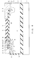
- An n-type silicon active layer (SOI semiconductor film) 3 having a high resistance (low concentration) is arranged on a silicon supporting body 1 through a silicon oxide film (SOI insulating film) 2.
- An SOI substrate is constituted by the silicon supporting body 1, silicon oxide film 2, and n-type silicon active layer 3.
- the n-type silicon active layer 3 is used as an n-type drift layer 4. Note that it is not essential for the n-type drift layer 4 to be in direct contact with the silicon oxide film 2. For example, an n-type layer having a low resistance may be arranged in the n-type silicon active layer 3 between the n-type drift layer 4 and the silicon oxide film 2.
- First and second p-type base layers 11 and 14 having a strip shape are selectively formed in the surface of the n-type drift layer 4 so as to sandwich therebetween an intervening portion 4a which is part of the n-type drift layer 4.
- First and second n-type source layers 13 and 15 having a low resistance (high concentration) are respectively and selectively formed in the surface of the first and second p-type base layer 11 and 14.
- the first n-type source layer 13 has a strip shape
- the second n-type source layer 15 has a strip shape resembling a ladder, as shown in FIG. 1.
- the p-type base layers 11 and 14 are arranged separate from each other along a direction which is prevailing in lines connecting the n-type source layers 13 and 15 to a p-type drain layer described later.
- This separating direction can be considered as a prevailing direction along which electrons drift between the source and drain, i.e., drifting direction.
- a main gate electrode 18 is arranged to face, through a gate oxide film 17, a surface of the second p-type base layer 14 which is interposed between the second n-type source layer 15 and the n-type drift layer 4.
- a sub-gate electrode 20 is arranged, through a gate oxide film 19, over a surface between the first and second n-type source layer 13 and 15.
- the sub-gate electrode 20 faces, through the gate oxide film 19, a surface of the first p-type base layer 11 which is interposed between the first n-type source layer 13 and the intervening portion 4a of the n-type drift layer 4, and also faces, through the gate oxide film 19, a surface of the second p-type base layer 14 which is interposed between the second n-type source layer 15 and the intervening portion 4a of the n-type drift layer 4.
- three n-type MOSFETs are constituted so as to form three n-type channels, one of which is in the first p-type base layer 11 while two of which are in the second p-type base layer 14.
- the main gate electrode 18 and sub-gate electrode 20 may be formed integral, or may be formed independent of each other with, e.g., an Al wiring layer electrically connecting them.
- a source electrode 21 is arranged on the first and second n-type source layers 13 and 15 and the first and second p-type base layers 11 and 14.
- the source electrode 21 is in contact with the first p-type base layer 11 through a p-type contact layer 12 having a low resistance, and is also in contact with the second p-type base layer 14 through a p-type contact layer 16 having a low resistance.
- An n-type buffer layer 6 is selectively formed in the n-type drift layer 4 and is separated from the p-type base layer 14 by a predetermined distance.
- a p-type drain layer 7 is selectively formed in a surface of the n-type buffer layer 6.
- a p-type contact layer 8 and an n-type layer 9 each having a low resistance are selectively formed in the surface of the p-type drain layer 7.
- a drain electrode 10 is arranged on the p-type contact layer 8 and the n-type layer 9. The drain electrode 10 is in contact with the p-type drain layer 7 through the p-type contact layer 8.
- the n-type layer 9 works for decreasing the drain injection efficiency, i.e., injection efficiency of holes from the p-type drain layer 7, so that a turn-off operation is performed at a high speed.
- FIGS. 1 and 2 there are also shown an embedded insulating film 3a for trench isolation, insulating films (oxide films) 5 and 24, and contact holes 22 and 23 for forming contacts between the p-type base layer 11 and the source electrode 21 and between the p-type base layer 14 and the source electrode 21, respectively.
- the contact hole 23 is strip shaped. With this arrangement, since the second n-type source layer 15 has a ladder shape, the width W1 of the p-type base layer 14 can be small.
- the contact hole 22 is also strip shaped.
- three n-type channels can be formed by the three n-type MOSFET formed of the first and second p-type base layers 11 and 14 and so forth.
- the channel width is effectively increased thereby lowering the resistance of the channels as a whole, as compared with a conventional lateral IGBT which has only one n-type channel. It follows that the current density per unit surface area is increased, thereby allowing a chip size to be compact.
- the width W1 of the second p-type base layer 14 should be small for increasing the current density. More specifically, the width W1 is set preferably at 10 ⁇ m or less. Where the width is set at 6 ⁇ m or less, the current density becomes about twice as large.
- the depth D1 of the second p-type base layer 14 should be small.
- the depth D1 is set preferably at 6 ⁇ m or less, and more preferably at 4 ⁇ m or less.
- the thickness T SOI of the n-type drift layer 4 grows larger, electrons from a channel more distant from the drain are caused to be injected more easily, thereby enhancing the effects of the present invention.
- the thickness T SOI is set preferably at 7 ⁇ m or more, and more preferably at 10 ⁇ m or more. By doing so, the effects of arranging a plurality of channels are further enhanced.
- the thickness T SOI should be set to satisfy W1 ⁇ T SOI .
- the distance between the first and second p-type base layers 11 and 14, i.e., the width W2 of the intervening portion 4a is set preferably at 7 ⁇ m or more, and more preferably at 10 ⁇ m or more. With this arrangement, resistance in the depth direction, i.e., vertical resistance, within the channel region is decreased, thereby improving device properties.
- the width W2 should be set to satisfy W2 ⁇ D1. With this relationship, it is possible to decrease resistance in the depth direction within the intervening portion 4a, when a depletion layer is formed to extend from the p-type base layer into the n-type drift layer 4.
- the current during application of a high voltage is decreased, so that the device is hardly broken when a resistor connected to the device is short-circuited. More specifically, if the resistor is short-circuited, a power supply voltage is directly applied to the device. For example, a power supply of DC 300V is used, a voltage drop of 300V is caused in the device while the gates are turned on, thereby causing a large current to flow through the device. In order to protect the device from this large current, the device should limit the current flowing therethrough by itself.
- the gate oxide films 17 and 19 are set thin, a gate voltage can be decreased, so that the ON resistance of the device is decreased.
- a voltage drop within a channel formed by application of the gate voltage is beyond the gate voltage, the current flowing through the device is not increased any more.
- the current, which flows when the resistor is short-circuited can be decreased by lowering the gate voltage.
- the generated heat becomes small, so that the device is not broken for a short period of time. If a device protection circuit can detect this abnormal state and shut down the device within this short period of time, the device is not broken. This effect is enhanced, where the gate oxide films 17 and 19 are set at 60 nm or less, and more preferably at 30 nm or less.
- the SOI substrate having the silicon substrate 1, silicon oxide film 2, and n-type silicon layer 3 is formed by means of a direct bonding method.
- the thickness of the n-type silicon layer 3 is set at, e.g., about 10 ⁇ m.
- trenches are formed in the n-type silicon layer 3 to reach the silicon oxide film 2, and the embedded insulating films 3a are formed in the trenches, so that a power device (IGBT) region, i.e., the drift layer 4 is isolated.
- IGBT power device
- the entire exposed surface of the n-type drift layer is oxidized to form a thin oxide film having a thickness of about 0.1 ⁇ m. Further, a nitride film is formed on the oxide film. Then, the oxide and nitride films are removed except for the source and drain regions.
- the overall surface is subjected to oxidation, so that the thick oxide film 24 having a thickness of about 1 ⁇ m is formed outside the regions where the nitride film is left.
- the nitride film is removed and the n-type buffer layer 6 is formed by means of diffusion. Then, the thin oxide film is removed and the gate oxide films 17 and 19 are formed.
- a polysilicon film is formed and patterned to form the gate electrodes 18 and 20.
- the p-type base layers 11 and 14, and p-type drain layer 7, which have a depth of about 4 ⁇ m, are formed, using the gate electrodes 18 and 20, and oxide film 24 as masks.
- p-type contact layers 12 and 16 are formed by means of ion implantation of boron at a dose of 1 ⁇ 10 15 cm -2 .
- the n-type source layers 13 and 15, and the n-type layer 9 are formed by means of diffusion, and the p-type contact layer 8 is formed by means of diffusion, using the gate electrodes 18 and 20, and oxide film 24 as masks.
- the oxide film 5 is formed overall and patterned along with other insulating films, so that the contact holes are formed.
- drain and source electrodes 10 and 21 are formed to complete the lateral IGBT.
- the drain electrode 10 is formed such that the effect of a field plate is obtained.
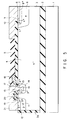
- FIG. 3 is a cross sectional view schematically a lateral IGBT according to another embodiment of the present invention.
- the parts corresponding to those of the lateral IGBT shown in FIG. 2 are provided with reference symbols the same as those in FIG. 2, and their detailed explanation will be omitted. In the drawings after FIG.3, this is done in the same manner.
- the lateral IGBT according to this embodiment differs from the embodiment shown in FIG. 2 in that a shallow n-type diffusion layer 25 is formed in a surface of an intervening portion 4a arranged under a sub-gate electrode 20. With this arrangement, the gate region has a small resistance in the depth direction, so that the ON resistance of the device is decreased.
- the n-type diffusion layer 25 overlaps p-type base layers 11 and 14.
- FIG. 4 is a cross sectional view schematically a lateral IGBT according to still another embodiment of the present invention.
- the lateral IGBT according to this embodiment differs from the embodiment shown in FIG. 2 in that a deep n-type diffusion layer 25a having a low resistance is formed in a surface of an intervening portion 4a arranged under a sub-gate electrode 20. With this arrangement, the gate region has a small resistance in the depth direction, so that the ON resistance of the device is decreased.
- the n-type diffusion layer 25a does not overlap p-type base layers 11 and 14.
- FIG. 5 is a cross sectional view schematically a lateral IGBT according to still another embodiment of the present invention.
- the lateral IGBT according to this embodiment differs from the embodiment shown in FIG. 2 in that a source electrode 21 penetrates an n-type source layer 15 and is in contact with a p-type base layer 14 through a p-type contact layer 16.
- a contact between the source electrode 21 and the p-type base layer 14 is formed, using a shallow trench.
- the p-type base layer 14 has a small resistance (lateral resistance) between the source electrode 21 and a portion right under the n-type source layer 15 closest to the drain, so that a latch-up phenomenon is effectively prevented.
- FIG. 6 is a plan view schematically a lateral IGBT according to still another embodiment of the present invention.
- the lateral IGBT according to this embodiment differs from the embodiment shown in FIG. 2 in that an n-type source layer 13 is formed as islands.
- n-type channels are formed in a direction parallel to the drifting direction, as well as a direction perpendicular to the drifting direction, so that the channel width is increased and the ON resistance of the device is lowered, thereby improving the current driving performance.
- the present invention is not limited to the above described embodiments.
- the number of p-type base layers may be three or more to further increase the number of channels, so that the current density may be further increased.
- each of a p-type base layer and an n-type source layer has two portions facing each other with an intervening portion 4a, which is part of an n-type drift layer 4, interposed therebetween, and a sub-gate electrode 20 is arranged thereon, so that the channel resistance of the device is lowered as a whole.
- the lateral IGBT can increase the amount of current by 30% or more, as compared to a conventional IGBT having a main gate electrode only.
- the surface area of the device is increased by a certain degree corresponding to the source region enlarged by adding the sub-gate electrode 20. Since the current density of a lateral device is defined on the basis of a surface area including the source, drift and drain regions, it is preferable to set the source region smaller in order to increase the current density.
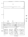
- two different lateral IGBTs are provided according to still other embodiments of the present invention, each of which has first and second device units DU1 and DU2 arranged side by side.
- each of the device units DU1 and DU2 has source, drift and drain regions 31, 32 and 33, as in the lateral IGBT shown in FIG. 2.
- each of the device units has three n-type MOSFETs, one of which corresponds to a main gate 18, and the other two correspond to a sub-gate electrode 20.
- the device units DU1 and DU2 commonly own an intervening portion 4a, which is part of an n-type drift layer 4, and a sub-gate electrode 20.
- the third n-type MOSFET of the device unit DU1 which is most distant from the drain region 33 of the device unit DU1, works as the second n-type MOSFET of the adjacent device unit DU2.
- a current flowing through a channel formed by the third n-type MOSFET of one device unit basically becomes a current flowing in an adjacent device unit.
- the amount of the current flowing through the third channel is much smaller than the amount of currents flowing through the first and second channels. Consequently, a voltage drop caused in each of the device units by commonly using the intervening portion 4a and the sub-gate electrode 20 is not so large. Instead, since the width of the source region is decreased with the current amount scarcely reduced, the current density is improved as a whole. Further, the currents respectively flowing through the channels become uniform, so that a latch-up phenomenon is hardly caused and the withstand capacity of the device upon short-circuiting of a resistor is increased.
- each of the p-type base layer and the n-type source layer may be divided into two portions facing each other through the intervening portion 4a, as shown in FIGS. 1 and 6.
- the two portions of the p-type base layer facing each other through the intervening portion 4a may consist of two opposite portions of an integrated single layer.
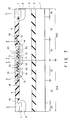
- an intervening portion 4a which is part of an n-type drift layer 4, is arranged at the center, and a p-type base layer 14, an n-type source layer 15, the drift layer 4, a drain layer 7, and so forth, each having a ring shape, are coaxially arranged.
- a base layer 14 is formed to surround a drain layer 7.
- the structure shown in FIG. 17 provides a higher withstand capacity against a latch-up phenomenon, so that it can be turned off even at a large current. The reason of this is as follows.
- FIGS. 9 and 17 Note that a cross sectional view of each of the lateral IGBTs shown in FIGS. 9 and 17 is substantially the same as that shown in FIG. 8.
- a substrate having an n-type silicon active layer 3 arranged on a silicon supporting body 1 through a silicon oxide film 2 was used as a sample substrate for the simulations.
- a drifting length L1 was set at 60 ⁇ m, the thickness T1 of the active layer 3 at 15 ⁇ m, and the thickness T2 of the oxide film 2 at 3 ⁇ m (see FIG. 10), for obtaining a breakdown voltage of 500V.
- the impurity concentration of the active layer 3 was set at 9.3 ⁇ 10 14 cm -3 , since it was known that a high breakdown voltage could be obtained at an implantation dose of about 1 ⁇ 10 12 cm -2 .
- a preprocessor MEDIT was employed for forming device structure data.
- a two dimensional device simulator TONADDE2C was employed for simulating current-voltage characteristics.
- a post-processor VECTOR was employed for outputting current lines used for analyzing characteristics.
- FIG. 11 is a graph showing a simulation result in terms of a characteristic of current densities to voltages.
- Three lines shown in FIG. 11 denote characteristics of a present sample PS1 of the present invention having three channels formed by a main gate electrode 18 and a sub-gate electrode 20, a comparative sample CS1 having only one channel formed by the main gate electrode 18, and a comparative sample CS2 having only two channels formed by the sub-gate electrode 20, respectively.
- Each channel length was set at 1.0 ⁇ m, a sub-gate length L2 at 5 ⁇ m, and a gate-gap length L3 at 6 ⁇ m (see FIg. 10). Note that the sub-gate length L2 and the gate-gap length L3 were used as parameters approximate to the width W2 of the intervening portion 4a and the width W1 of the second p-type base layer 14, respectively, shown in FIG. 2.
- FIG. 12 is a graph showing another simulation result in terms of a characteristic of current densities to voltages.
- Two lines shown in FIG. 12 denote characteristics of a present sample PS2 of the present invention having three channels formed by the main gate electrode 18 and the sub-gate electrode 20, and a comparative sample CS3 having only one channel formed by the main gate electrode 18, respectively.
- the simulation of FIG. 12 was conducted under conditions the same as those of the simulation of FIG. 11, except that the sub-gate length L2 was set at 10 ⁇ m and the concentration in the surface of the p-type base layer was set slightly high. Namely, each channel length was set at 1.0 ⁇ m, and the gate-gap length L3 at 6 ⁇ m.
- FIG. 13 is a graph showing a simulation result in terms of the influence of the sub-gate length L2 on a characteristic of current densities to voltages.
- Three lines shown in FIG. 13 denote characteristics of present samples PS2, PS3 and PS4, respectively, of the present invention having three channels formed by the main gate electrode 18 and the sub-gate electrode 20.
- the sub-gate length L2 was set at 10 ⁇ m, 5 ⁇ m and 15 ⁇ m in the samples PS2, PS3 and PS4, respectively.
- the simulation of FIG. 13 was conducted under conditions the same as those of the simulation of FIG. 12, except that the sub-gate length L2 was changed. Namely, each channel length was set at 1.0 ⁇ m, and the gate-gap length L3 at 6 ⁇ m.
- the current passage has a thickness T CP (see FIG. 10) of 10 ⁇ m to 14 ⁇ m in the n-type drift layer 4 under the p-type base layers 11 and 14, judging from the active layer 3 having a thickness of 15 ⁇ m, and the p-type base layers 11 and 14 having a thickness of 1 ⁇ m to 5 ⁇ m. Therefore, where the sub-gate length L2 is set at 10 ⁇ m, the current passage has almost the same thicknesses under the p-type base layer 11 and 14, and right under the sub-gate electrode 20, i.e., at the intervening portion 4a. As a result, the sample PS2 produces a current density as large as 162% of that produced by the sample CS3 (a conventional structure).
- the current passage which has a thickness of 10 ⁇ m to 14 ⁇ m under the p-type base layers 11 and 14, abruptly becomes narrower right under the sub-gate electrode 20, i.e., at the intervening portion 4a. As a result, an effect of the increased number of channels is not sufficiently utilized.
- the current passage becomes larger right under the sub-gate electrode 20, i.e., at the intervening portion 4a, but has a limited thickness under the p-type base layers 11 and 14. As a result, an effect of the large sub-gate length L2 is not sufficiently utilized.
- the thickness of the n-type drift layer 4 under the p-type base layer 11 and 14, and the width of the intervening portion 4a right under the sub-gate electrode 20 should be approximate to each other.
- FIG. 14 is a graph showing a simulation result in terms of the influence of the gate-gap length L3 on a characteristic of current densities to voltages.
- Three lines shown in FIG. 14 denote characteristics of present samples PS2, PS5 and PS6, respectively, of the present invention having three channels formed by the main gate electrode 18 and the sub-gate electrode 20.
- the gate-gap length L3 was set at 6 ⁇ m, 3 ⁇ m and 10 ⁇ m in the samples PS2, PS5 and PS6, respectively.
- the simulation of FIG. 14 was conducted under conditions the same as those of the simulation of FIG. 12, except that the gate-gap length L3 was changed. Namely, each channel length was set at 1.0 ⁇ m, and the sub-gate length L2 at 10 ⁇ m.
- FIG. 15 is a graph showing a simulation result in terms of the influence of the number of channels (the number of MOSFETs) on a characteristic of current densities to voltages.
- Three lines shown in FIG. 15 denote characteristics of a present sample PS2 of the present invention having three channels formed by the main gate electrode 18 and the sub-gate electrode 20, a present sample PS7 of the present invention having five channels formed by the main gate electrode 18 and two sub-gate electrodes 20, and a comparative sample CS3 having only one channel formed by the main gate electrode 18, respectively.
- MOSFETs formed by the second sub-gate electrode 20 of the sample PS7 were arranged on a side distant from the drain. The simulation of FIG. 15 was conducted under conditions the same as those of the simulation of FIG.
- each channel length was set at 1.0 ⁇ m, the sub-gate length L2 at 10 ⁇ m and the gate-gap length L3 at 6 ⁇ m.
- the sample PS2 of the present invention having three channels produced a current density as large as 162% of that produced by the sample CS3 (a conventional structure) having only one channel.
- the sample PS7 of the present invention having five channels produced a current density lower than that of the sample PS2. This phenomenon is thought to have been caused due to the following reason.
- the number of channels is five, the drifting length of two channels most distant from the drain is large, and the amount of a current flowing through the two channels into the second sub-gate electrode is very small. Further, where the number of channels is five, the entire length of the device, which is a parameter in calculation of the current density, is increased. As a result, the current density is decreased even though the number of channels is increased.
- FIG. 16 is a graph showing a simulation result in terms of the influence of each channel length on a characteristic of current densities to voltages.
- Three lines shown in FIG. 16 denote characteristics of present samples PS8, PS9 and PS10, respectively, of the present invention having three channels formed by the main gate electrode 18 and the sub-gate electrode 20.
- Each channel length was set at 1.0 ⁇ m, 2.2 ⁇ m and 3.0 ⁇ m in the samples PS8, PS9 and PS10, respectively.
- the sub-gate length L2 was set at 12 ⁇ m in the samples PS8, PS9 and PS10.
- the simulation of FIG. 16 was conducted under conditions the same as those of the simulation of FIG. 12, except that each channel length and the sub-gate length L2 were changed. Namely, the gate-gap length L3 was at 6 ⁇ m.
- the current density was increased with a decrease in each channel length. From this result, it has been found that the current density can be greatly improved by adopting a short-channel structure in the device of the present invention.
- a MOSFET constituted by a sub-gate electrode and so forth is added, a plurality of channels are arranged. As a result, the channel width is effectively enlarged, so that the current density is increased.
Applications Claiming Priority (3)
| Application Number | Priority Date | Filing Date | Title |
|---|---|---|---|
| JP21635095 | 1995-08-24 | ||
| JP216350/95 | 1995-08-24 | ||
| JP21635095 | 1995-08-24 |
Publications (3)
| Publication Number | Publication Date |
|---|---|
| EP0760529A2 true EP0760529A2 (de) | 1997-03-05 |
| EP0760529A3 EP0760529A3 (de) | 1997-10-15 |
| EP0760529B1 EP0760529B1 (de) | 2002-12-18 |
Family
ID=16687182
Family Applications (1)
| Application Number | Title | Priority Date | Filing Date |
|---|---|---|---|
| EP96306166A Expired - Lifetime EP0760529B1 (de) | 1995-08-24 | 1996-08-23 | Lateraler IGBT |
Country Status (3)
| Country | Link |
|---|---|
| US (2) | US5731603A (de) |
| EP (1) | EP0760529B1 (de) |
| DE (1) | DE69625417T2 (de) |
Cited By (4)
| Publication number | Priority date | Publication date | Assignee | Title |
|---|---|---|---|---|
| FR2767967A1 (fr) * | 1997-06-13 | 1999-03-05 | Bosch Gmbh Robert | Composant transistor |
| DE19836233B4 (de) * | 1998-08-05 | 2008-10-30 | X-Fab Semiconductor Foundries Ag | Lateraler DMOS-Transistor auf isolierender Unterlage und Verfahren zu seiner Herstellung |
| CN102956636A (zh) * | 2012-09-14 | 2013-03-06 | 东南大学 | 一种大电流n型绝缘体上硅横向绝缘栅双极型晶体管 |
| EP3240039A4 (de) * | 2014-12-22 | 2018-08-01 | CSMC Technologies Fab1 Co., Ltd. | Bipolarer transistor mit seitlichem isoliertem gate |
Families Citing this family (78)
| Publication number | Priority date | Publication date | Assignee | Title |
|---|---|---|---|---|
| US6064086A (en) * | 1995-08-24 | 2000-05-16 | Kabushiki Kaisha Toshiba | Semiconductor device having lateral IGBT |
| US5977569A (en) * | 1996-09-24 | 1999-11-02 | Allen-Bradley Company, Llc | Bidirectional lateral insulated gate bipolar transistor having increased voltage blocking capability |
| US6133607A (en) * | 1997-05-22 | 2000-10-17 | Kabushiki Kaisha Toshiba | Semiconductor device |
| JP3147048B2 (ja) * | 1997-09-12 | 2001-03-19 | 日本電気株式会社 | 半導体装置 |
| DE19820956A1 (de) * | 1998-05-11 | 1999-11-18 | Daimler Chrysler Ag | Halbleiter-Bauelement und Verfahren zu seiner Herstellung sowie Verwendung des Halbleiter-Bauelements |
| DE19828669C2 (de) * | 1998-06-26 | 2003-08-21 | Infineon Technologies Ag | Lateraler IGBT in SOI-Bauweise und Verfahren zur Herstellung |
| SE9901575L (sv) * | 1999-05-03 | 2000-11-04 | Eklund Klas Haakan | Halvledarelement |
| JP2001094094A (ja) * | 1999-09-21 | 2001-04-06 | Hitachi Ltd | 半導体装置およびその製造方法 |
| JP4357127B2 (ja) | 2000-03-03 | 2009-11-04 | 株式会社東芝 | 半導体装置 |
| EP1442482A1 (de) * | 2001-11-01 | 2004-08-04 | Koninklijke Philips Electronics N.V. | Bipolartransistorbauelement mit seitlich isoliertem gate |
| US8067855B2 (en) * | 2003-05-06 | 2011-11-29 | Enecsys Limited | Power supply circuits |
| EP1623495B1 (de) | 2003-05-06 | 2009-10-07 | Enecsys Limited | Stromversorgungsschaltungen |
| US7329566B2 (en) | 2005-05-31 | 2008-02-12 | Freescale Semiconductor, Inc. | Semiconductor device and method of manufacture |
| US7244989B2 (en) * | 2005-06-02 | 2007-07-17 | Freescale Semiconductor, Inc. | Semiconductor device and method of manufacture |
| US7180158B2 (en) * | 2005-06-02 | 2007-02-20 | Freescale Semiconductor, Inc. | Semiconductor device and method of manufacture |
| US11881814B2 (en) | 2005-12-05 | 2024-01-23 | Solaredge Technologies Ltd. | Testing of a photovoltaic panel |
| US10693415B2 (en) | 2007-12-05 | 2020-06-23 | Solaredge Technologies Ltd. | Testing of a photovoltaic panel |
| JP2007194575A (ja) * | 2005-12-21 | 2007-08-02 | Mitsubishi Electric Corp | 半導体装置 |
| JP4257346B2 (ja) * | 2006-06-27 | 2009-04-22 | 株式会社東芝 | 電力増幅器 |
| US11728768B2 (en) | 2006-12-06 | 2023-08-15 | Solaredge Technologies Ltd. | Pairing of components in a direct current distributed power generation system |
| US11855231B2 (en) | 2006-12-06 | 2023-12-26 | Solaredge Technologies Ltd. | Distributed power harvesting systems using DC power sources |
| US8816535B2 (en) | 2007-10-10 | 2014-08-26 | Solaredge Technologies, Ltd. | System and method for protection during inverter shutdown in distributed power installations |
| US9088178B2 (en) | 2006-12-06 | 2015-07-21 | Solaredge Technologies Ltd | Distributed power harvesting systems using DC power sources |
| US8319483B2 (en) | 2007-08-06 | 2012-11-27 | Solaredge Technologies Ltd. | Digital average input current control in power converter |
| US8947194B2 (en) | 2009-05-26 | 2015-02-03 | Solaredge Technologies Ltd. | Theft detection and prevention in a power generation system |
| US11888387B2 (en) | 2006-12-06 | 2024-01-30 | Solaredge Technologies Ltd. | Safety mechanisms, wake up and shutdown methods in distributed power installations |
| US11309832B2 (en) | 2006-12-06 | 2022-04-19 | Solaredge Technologies Ltd. | Distributed power harvesting systems using DC power sources |
| US9112379B2 (en) | 2006-12-06 | 2015-08-18 | Solaredge Technologies Ltd. | Pairing of components in a direct current distributed power generation system |
| US9130401B2 (en) | 2006-12-06 | 2015-09-08 | Solaredge Technologies Ltd. | Distributed power harvesting systems using DC power sources |
| US11569659B2 (en) | 2006-12-06 | 2023-01-31 | Solaredge Technologies Ltd. | Distributed power harvesting systems using DC power sources |
| WO2009073868A1 (en) | 2007-12-05 | 2009-06-11 | Solaredge, Ltd. | Safety mechanisms, wake up and shutdown methods in distributed power installations |
| US8319471B2 (en) | 2006-12-06 | 2012-11-27 | Solaredge, Ltd. | Battery power delivery module |
| US8384243B2 (en) | 2007-12-04 | 2013-02-26 | Solaredge Technologies Ltd. | Distributed power harvesting systems using DC power sources |
| US11735910B2 (en) | 2006-12-06 | 2023-08-22 | Solaredge Technologies Ltd. | Distributed power system using direct current power sources |
| US8618692B2 (en) | 2007-12-04 | 2013-12-31 | Solaredge Technologies Ltd. | Distributed power system using direct current power sources |
| US11296650B2 (en) | 2006-12-06 | 2022-04-05 | Solaredge Technologies Ltd. | System and method for protection during inverter shutdown in distributed power installations |
| US8963369B2 (en) | 2007-12-04 | 2015-02-24 | Solaredge Technologies Ltd. | Distributed power harvesting systems using DC power sources |
| US8473250B2 (en) | 2006-12-06 | 2013-06-25 | Solaredge, Ltd. | Monitoring of distributed power harvesting systems using DC power sources |
| US8013472B2 (en) | 2006-12-06 | 2011-09-06 | Solaredge, Ltd. | Method for distributed power harvesting using DC power sources |
| US11687112B2 (en) | 2006-12-06 | 2023-06-27 | Solaredge Technologies Ltd. | Distributed power harvesting systems using DC power sources |
| JP4458112B2 (ja) * | 2007-04-18 | 2010-04-28 | 株式会社日立製作所 | 半導体装置の製造方法、それを用いた半導体装置及びプラズマパネルディスプレイ |
| US11264947B2 (en) | 2007-12-05 | 2022-03-01 | Solaredge Technologies Ltd. | Testing of a photovoltaic panel |
| WO2009073867A1 (en) | 2007-12-05 | 2009-06-11 | Solaredge, Ltd. | Parallel connected inverters |
| US8049523B2 (en) | 2007-12-05 | 2011-11-01 | Solaredge Technologies Ltd. | Current sensing on a MOSFET |
| US9291696B2 (en) | 2007-12-05 | 2016-03-22 | Solaredge Technologies Ltd. | Photovoltaic system power tracking method |
| US7960950B2 (en) | 2008-03-24 | 2011-06-14 | Solaredge Technologies Ltd. | Zero current switching |
| JP2009260119A (ja) * | 2008-04-18 | 2009-11-05 | Panasonic Corp | 半導体装置、及び該半導体装置を用いたエネルギー伝達装置 |
| US9000617B2 (en) | 2008-05-05 | 2015-04-07 | Solaredge Technologies, Ltd. | Direct current power combiner |
| US8354710B2 (en) * | 2008-08-08 | 2013-01-15 | Infineon Technologies Ag | Field-effect device and manufacturing method thereof |
| JP2011181709A (ja) * | 2010-03-02 | 2011-09-15 | Hitachi Ltd | 半導体装置およびその製造方法 |
| JP5636848B2 (ja) | 2010-05-26 | 2014-12-10 | 株式会社デンソー | 横型の絶縁ゲート型バイポーラトランジスタ |
| US10673222B2 (en) | 2010-11-09 | 2020-06-02 | Solaredge Technologies Ltd. | Arc detection and prevention in a power generation system |
| GB2485527B (en) | 2010-11-09 | 2012-12-19 | Solaredge Technologies Ltd | Arc detection and prevention in a power generation system |
| US10230310B2 (en) | 2016-04-05 | 2019-03-12 | Solaredge Technologies Ltd | Safety switch for photovoltaic systems |
| US10673229B2 (en) | 2010-11-09 | 2020-06-02 | Solaredge Technologies Ltd. | Arc detection and prevention in a power generation system |
| GB2486408A (en) | 2010-12-09 | 2012-06-20 | Solaredge Technologies Ltd | Disconnection of a string carrying direct current |
| GB2483317B (en) | 2011-01-12 | 2012-08-22 | Solaredge Technologies Ltd | Serially connected inverters |
| US8570005B2 (en) | 2011-09-12 | 2013-10-29 | Solaredge Technologies Ltd. | Direct current link circuit |
| JP5902949B2 (ja) * | 2012-01-05 | 2016-04-13 | 株式会社 日立パワーデバイス | 半導体装置 |
| GB2498365A (en) | 2012-01-11 | 2013-07-17 | Solaredge Technologies Ltd | Photovoltaic module |
| GB2498790A (en) | 2012-01-30 | 2013-07-31 | Solaredge Technologies Ltd | Maximising power in a photovoltaic distributed power system |
| GB2498791A (en) | 2012-01-30 | 2013-07-31 | Solaredge Technologies Ltd | Photovoltaic panel circuitry |
| US9853565B2 (en) | 2012-01-30 | 2017-12-26 | Solaredge Technologies Ltd. | Maximized power in a photovoltaic distributed power system |
| GB2499991A (en) | 2012-03-05 | 2013-09-11 | Solaredge Technologies Ltd | DC link circuit for photovoltaic array |
| US10529866B2 (en) | 2012-05-30 | 2020-01-07 | X-Fab Semiconductor Foundries Gmbh | Semiconductor device |
| US8735937B2 (en) | 2012-05-31 | 2014-05-27 | Taiwan Semiconductor Manufacturing Company, Ltd. | Fully isolated LIGBT and methods for forming the same |
| US10115841B2 (en) | 2012-06-04 | 2018-10-30 | Solaredge Technologies Ltd. | Integrated photovoltaic panel circuitry |
| CN102903746B (zh) * | 2012-11-07 | 2015-06-03 | 东南大学 | 一种大电流密度的横向超薄绝缘栅双极型晶体管 |
| US9941813B2 (en) | 2013-03-14 | 2018-04-10 | Solaredge Technologies Ltd. | High frequency multi-level inverter |
| US9548619B2 (en) | 2013-03-14 | 2017-01-17 | Solaredge Technologies Ltd. | Method and apparatus for storing and depleting energy |
| EP3506370B1 (de) | 2013-03-15 | 2023-12-20 | Solaredge Technologies Ltd. | Bypass-mechanismus |
| CN104347691B (zh) * | 2013-07-24 | 2017-05-24 | 旺宏电子股份有限公司 | 半导体装置及其操作方法 |
| CN104737293B (zh) * | 2013-12-23 | 2017-05-03 | 伍震威 | 用于功率半导体装置的场板结构及其制造方法 |
| US9318974B2 (en) | 2014-03-26 | 2016-04-19 | Solaredge Technologies Ltd. | Multi-level inverter with flying capacitor topology |
| US11018623B2 (en) | 2016-04-05 | 2021-05-25 | Solaredge Technologies Ltd. | Safety switch for photovoltaic systems |
| US11177663B2 (en) | 2016-04-05 | 2021-11-16 | Solaredge Technologies Ltd. | Chain of power devices |
| EP3279935B1 (de) * | 2016-08-02 | 2019-01-02 | ABB Schweiz AG | Leistungshalbleitermodul |
| CN112825301B (zh) * | 2019-11-21 | 2022-08-12 | 东南大学 | 绝缘栅双极型晶体管器件及其制造方法 |
Citations (5)
| Publication number | Priority date | Publication date | Assignee | Title |
|---|---|---|---|---|
| EP0094891A2 (de) * | 1982-05-20 | 1983-11-23 | Fairchild Semiconductor Corporation | Verfahren zur Herstellung einer vertikalen Leistungs-MOSFET-Struktur |
| EP0280535A2 (de) * | 1987-02-26 | 1988-08-31 | Kabushiki Kaisha Toshiba | MOS-Feldeffekt-Transistor mit Leitfähigkeitsmodulation |
| JPH02109371A (ja) * | 1988-10-19 | 1990-04-23 | Hitachi Ltd | 導電変調型mosデバイス |
| DE4006886A1 (de) * | 1989-03-06 | 1990-09-13 | Fuji Electric Co Ltd | Halbleiter-vorrichtung mit einem mis-feldeffekt-transistor von der art einer leitfaehigkeits-modulation |
| DE4104588A1 (de) * | 1990-02-14 | 1991-08-22 | Fuji Electric Co Ltd | Halbleiterbauelement mit einem leitfaehigkeitsmodulations-misfet |
Family Cites Families (2)
| Publication number | Priority date | Publication date | Assignee | Title |
|---|---|---|---|---|
| JPH0693512B2 (ja) * | 1986-06-17 | 1994-11-16 | 日産自動車株式会社 | 縦形mosfet |
| JPH0396282A (ja) * | 1989-09-08 | 1991-04-22 | Fuji Electric Co Ltd | 絶縁ゲート型半導体装置 |
-
1996
- 1996-08-22 US US08/701,500 patent/US5731603A/en not_active Expired - Lifetime
- 1996-08-23 DE DE69625417T patent/DE69625417T2/de not_active Expired - Lifetime
- 1996-08-23 EP EP96306166A patent/EP0760529B1/de not_active Expired - Lifetime
-
1997
- 1997-11-13 US US08/970,103 patent/US5920087A/en not_active Expired - Fee Related
Patent Citations (5)
| Publication number | Priority date | Publication date | Assignee | Title |
|---|---|---|---|---|
| EP0094891A2 (de) * | 1982-05-20 | 1983-11-23 | Fairchild Semiconductor Corporation | Verfahren zur Herstellung einer vertikalen Leistungs-MOSFET-Struktur |
| EP0280535A2 (de) * | 1987-02-26 | 1988-08-31 | Kabushiki Kaisha Toshiba | MOS-Feldeffekt-Transistor mit Leitfähigkeitsmodulation |
| JPH02109371A (ja) * | 1988-10-19 | 1990-04-23 | Hitachi Ltd | 導電変調型mosデバイス |
| DE4006886A1 (de) * | 1989-03-06 | 1990-09-13 | Fuji Electric Co Ltd | Halbleiter-vorrichtung mit einem mis-feldeffekt-transistor von der art einer leitfaehigkeits-modulation |
| DE4104588A1 (de) * | 1990-02-14 | 1991-08-22 | Fuji Electric Co Ltd | Halbleiterbauelement mit einem leitfaehigkeitsmodulations-misfet |
Non-Patent Citations (2)
| Title |
|---|
| PATENT ABSTRACTS OF JAPAN vol. 014, no. 324 (E-0951), 11 July 1990 & JP 02 109371 A (HITACHI LTD), 23 April 1990, * |
| PROCEEDINGS OF THE INTERNATIONAL SYMPOSIUM ON POWER SEMICONDUCTOR DEVICES (ISPSD), DAVOS, CH, MAY 31 - JUNE 2, 1994, no. SYMP. 6, 31 May 1994, FICHTNER W (ED), pages 405-410, XP000505845 DISNEY D R ET AL: "A TRENCH-GATE LIGBT STRUCTURE AND TWO LMCT STRUCTURES IN SOI SUBSTRATES" * |
Cited By (5)
| Publication number | Priority date | Publication date | Assignee | Title |
|---|---|---|---|---|
| FR2767967A1 (fr) * | 1997-06-13 | 1999-03-05 | Bosch Gmbh Robert | Composant transistor |
| DE19836233B4 (de) * | 1998-08-05 | 2008-10-30 | X-Fab Semiconductor Foundries Ag | Lateraler DMOS-Transistor auf isolierender Unterlage und Verfahren zu seiner Herstellung |
| CN102956636A (zh) * | 2012-09-14 | 2013-03-06 | 东南大学 | 一种大电流n型绝缘体上硅横向绝缘栅双极型晶体管 |
| CN102956636B (zh) * | 2012-09-14 | 2015-02-04 | 东南大学 | 一种大电流n型绝缘体上硅横向绝缘栅双极型晶体管 |
| EP3240039A4 (de) * | 2014-12-22 | 2018-08-01 | CSMC Technologies Fab1 Co., Ltd. | Bipolarer transistor mit seitlichem isoliertem gate |
Also Published As
| Publication number | Publication date |
|---|---|
| US5920087A (en) | 1999-07-06 |
| EP0760529A3 (de) | 1997-10-15 |
| DE69625417T2 (de) | 2003-10-30 |
| DE69625417D1 (de) | 2003-01-30 |
| US5731603A (en) | 1998-03-24 |
| EP0760529B1 (de) | 2002-12-18 |
Similar Documents
| Publication | Publication Date | Title |
|---|---|---|
| US5731603A (en) | Lateral IGBT | |
| US6064086A (en) | Semiconductor device having lateral IGBT | |
| JP4744146B2 (ja) | 表面電界緩和型トランジスタを備える半導体部品 | |
| US6936893B2 (en) | Power semiconductor device | |
| US7968940B2 (en) | Insulated gate bipolar transistor device comprising a depletion-mode MOSFET | |
| US5760440A (en) | Back-source MOSFET | |
| KR100652449B1 (ko) | 횡형 박막 실리콘-온-절연체 jfet 디바이스 | |
| JP5357370B2 (ja) | 半導体デバイス | |
| EP0801425A1 (de) | Halbleiteranordnung mit isoliertem Gate und Verfahren zur Herstellung | |
| JPH04146674A (ja) | 半導体装置及びその製造方法 | |
| JP2001244461A (ja) | 縦型半導体装置 | |
| JP2000223707A (ja) | 横型絶縁ゲートバイポーラトランジスタ | |
| JP3293871B2 (ja) | 高耐圧半導体素子 | |
| JPS60253275A (ja) | 高密度v溝型mos制御型サイリスタ、絶縁ゲ−ト型トランジスタおよびmosfet、並びに製造方法 | |
| JPH09139438A (ja) | 半導体装置およびその製造方法 | |
| JP3730394B2 (ja) | 高耐圧半導体装置 | |
| US7276772B2 (en) | Semiconductor device | |
| JP2005209811A (ja) | 半導体装置 | |
| JPH08213617A (ja) | 半導体装置およびその駆動方法 | |
| JP3489404B2 (ja) | 絶縁ゲート型半導体装置 | |
| JPH0851197A (ja) | 電流飽和特性を有するmos制御サイリスタ | |
| JP4852188B2 (ja) | 半導体装置 | |
| EP1946380A2 (de) | Leistungshalbleiterbauelemente | |
| JPH09275212A (ja) | 電圧駆動型半導体装置 | |
| JP3522983B2 (ja) | 横型igbt |
Legal Events
| Date | Code | Title | Description |
|---|---|---|---|
| PUAI | Public reference made under article 153(3) epc to a published international application that has entered the european phase |
Free format text: ORIGINAL CODE: 0009012 |
|
| 17P | Request for examination filed |
Effective date: 19960913 |
|
| AK | Designated contracting states |
Kind code of ref document: A2 Designated state(s): DE FR GB |
|
| PUAL | Search report despatched |
Free format text: ORIGINAL CODE: 0009013 |
|
| AK | Designated contracting states |
Kind code of ref document: A3 Designated state(s): DE FR GB |
|
| 17Q | First examination report despatched |
Effective date: 20010816 |
|
| GRAG | Despatch of communication of intention to grant |
Free format text: ORIGINAL CODE: EPIDOS AGRA |
|
| GRAG | Despatch of communication of intention to grant |
Free format text: ORIGINAL CODE: EPIDOS AGRA |
|
| GRAH | Despatch of communication of intention to grant a patent |
Free format text: ORIGINAL CODE: EPIDOS IGRA |
|
| GRAH | Despatch of communication of intention to grant a patent |
Free format text: ORIGINAL CODE: EPIDOS IGRA |
|
| GRAA | (expected) grant |
Free format text: ORIGINAL CODE: 0009210 |
|
| AK | Designated contracting states |
Kind code of ref document: B1 Designated state(s): DE FR GB |
|
| PG25 | Lapsed in a contracting state [announced via postgrant information from national office to epo] |
Ref country code: FR Free format text: LAPSE BECAUSE OF FAILURE TO SUBMIT A TRANSLATION OF THE DESCRIPTION OR TO PAY THE FEE WITHIN THE PRESCRIBED TIME-LIMIT Effective date: 20021218 |
|
| REG | Reference to a national code |
Ref country code: GB Ref legal event code: FG4D |
|
| REF | Corresponds to: |
Ref document number: 69625417 Country of ref document: DE Date of ref document: 20030130 Kind code of ref document: P Ref document number: 69625417 Country of ref document: DE Date of ref document: 20030130 |
|
| PG25 | Lapsed in a contracting state [announced via postgrant information from national office to epo] |
Ref country code: GB Free format text: LAPSE BECAUSE OF NON-PAYMENT OF DUE FEES Effective date: 20030823 |
|
| PLBE | No opposition filed within time limit |
Free format text: ORIGINAL CODE: 0009261 |
|
| STAA | Information on the status of an ep patent application or granted ep patent |
Free format text: STATUS: NO OPPOSITION FILED WITHIN TIME LIMIT |
|
| EN | Fr: translation not filed | ||
| 26N | No opposition filed |
Effective date: 20030919 |
|
| GBPC | Gb: european patent ceased through non-payment of renewal fee | ||
| PGFP | Annual fee paid to national office [announced via postgrant information from national office to epo] |
Ref country code: DE Payment date: 20090821 Year of fee payment: 14 |
|
| REG | Reference to a national code |
Ref country code: DE Ref legal event code: R119 Ref document number: 69625417 Country of ref document: DE Effective date: 20110301 |
|
| PG25 | Lapsed in a contracting state [announced via postgrant information from national office to epo] |
Ref country code: DE Free format text: LAPSE BECAUSE OF NON-PAYMENT OF DUE FEES Effective date: 20110301 |