EP0748152A2 - Verfahren zum Montieren eines elektronischen Bauteils auf einem Leitersubstrat und beleuchteter Schalter unter Verwendung dieses Montierungsverfahrens - Google Patents
Verfahren zum Montieren eines elektronischen Bauteils auf einem Leitersubstrat und beleuchteter Schalter unter Verwendung dieses Montierungsverfahrens Download PDFInfo
- Publication number
- EP0748152A2 EP0748152A2 EP96304049A EP96304049A EP0748152A2 EP 0748152 A2 EP0748152 A2 EP 0748152A2 EP 96304049 A EP96304049 A EP 96304049A EP 96304049 A EP96304049 A EP 96304049A EP 0748152 A2 EP0748152 A2 EP 0748152A2
- Authority
- EP
- European Patent Office
- Prior art keywords
- electronic component
- insulating film
- mounting
- insulating
- terminals
- Prior art date
- Legal status (The legal status is an assumption and is not a legal conclusion. Google has not performed a legal analysis and makes no representation as to the accuracy of the status listed.)
- Granted
Links
Images


Classifications
-
- H—ELECTRICITY
- H05—ELECTRIC TECHNIQUES NOT OTHERWISE PROVIDED FOR
- H05K—PRINTED CIRCUITS; CASINGS OR CONSTRUCTIONAL DETAILS OF ELECTRIC APPARATUS; MANUFACTURE OF ASSEMBLAGES OF ELECTRICAL COMPONENTS
- H05K3/00—Apparatus or processes for manufacturing printed circuits
- H05K3/22—Secondary treatment of printed circuits
- H05K3/28—Applying non-metallic protective coatings
- H05K3/284—Applying non-metallic protective coatings for encapsulating mounted components
-
- H—ELECTRICITY
- H01—ELECTRIC ELEMENTS
- H01H—ELECTRIC SWITCHES; RELAYS; SELECTORS; EMERGENCY PROTECTIVE DEVICES
- H01H13/00—Switches having rectilinearly-movable operating part or parts adapted for pushing or pulling in one direction only, e.g. push-button switch
- H01H13/70—Switches having rectilinearly-movable operating part or parts adapted for pushing or pulling in one direction only, e.g. push-button switch having a plurality of operating members associated with different sets of contacts, e.g. keyboard
- H01H13/702—Switches having rectilinearly-movable operating part or parts adapted for pushing or pulling in one direction only, e.g. push-button switch having a plurality of operating members associated with different sets of contacts, e.g. keyboard with contacts carried by or formed from layers in a multilayer structure, e.g. membrane switches
-
- H—ELECTRICITY
- H05—ELECTRIC TECHNIQUES NOT OTHERWISE PROVIDED FOR
- H05K—PRINTED CIRCUITS; CASINGS OR CONSTRUCTIONAL DETAILS OF ELECTRIC APPARATUS; MANUFACTURE OF ASSEMBLAGES OF ELECTRICAL COMPONENTS
- H05K3/00—Apparatus or processes for manufacturing printed circuits
- H05K3/30—Assembling printed circuits with electric components, e.g. with resistor
- H05K3/32—Assembling printed circuits with electric components, e.g. with resistor electrically connecting electric components or wires to printed circuits
- H05K3/325—Assembling printed circuits with electric components, e.g. with resistor electrically connecting electric components or wires to printed circuits by abutting or pinching, i.e. without alloying process; mechanical auxiliary parts therefor
- H05K3/326—Assembling printed circuits with electric components, e.g. with resistor electrically connecting electric components or wires to printed circuits by abutting or pinching, i.e. without alloying process; mechanical auxiliary parts therefor the printed circuit having integral resilient or deformable parts, e.g. tabs or parts of flexible circuits
-
- H—ELECTRICITY
- H05—ELECTRIC TECHNIQUES NOT OTHERWISE PROVIDED FOR
- H05K—PRINTED CIRCUITS; CASINGS OR CONSTRUCTIONAL DETAILS OF ELECTRIC APPARATUS; MANUFACTURE OF ASSEMBLAGES OF ELECTRICAL COMPONENTS
- H05K3/00—Apparatus or processes for manufacturing printed circuits
- H05K3/30—Assembling printed circuits with electric components, e.g. with resistor
- H05K3/32—Assembling printed circuits with electric components, e.g. with resistor electrically connecting electric components or wires to printed circuits
- H05K3/34—Assembling printed circuits with electric components, e.g. with resistor electrically connecting electric components or wires to printed circuits by soldering
- H05K3/341—Surface mounted components
- H05K3/3421—Leaded components
-
- H—ELECTRICITY
- H01—ELECTRIC ELEMENTS
- H01H—ELECTRIC SWITCHES; RELAYS; SELECTORS; EMERGENCY PROTECTIVE DEVICES
- H01H2207/00—Connections
- H01H2207/032—Surface mounted component
-
- H—ELECTRICITY
- H01—ELECTRIC ELEMENTS
- H01H—ELECTRIC SWITCHES; RELAYS; SELECTORS; EMERGENCY PROTECTIVE DEVICES
- H01H2219/00—Legends
- H01H2219/036—Light emitting elements
- H01H2219/04—Attachments; Connections
-
- H—ELECTRICITY
- H05—ELECTRIC TECHNIQUES NOT OTHERWISE PROVIDED FOR
- H05K—PRINTED CIRCUITS; CASINGS OR CONSTRUCTIONAL DETAILS OF ELECTRIC APPARATUS; MANUFACTURE OF ASSEMBLAGES OF ELECTRICAL COMPONENTS
- H05K1/00—Printed circuits
- H05K1/18—Printed circuits structurally associated with non-printed electric components
- H05K1/189—Printed circuits structurally associated with non-printed electric components characterised by the use of a flexible or folded printed circuit
-
- H—ELECTRICITY
- H05—ELECTRIC TECHNIQUES NOT OTHERWISE PROVIDED FOR
- H05K—PRINTED CIRCUITS; CASINGS OR CONSTRUCTIONAL DETAILS OF ELECTRIC APPARATUS; MANUFACTURE OF ASSEMBLAGES OF ELECTRICAL COMPONENTS
- H05K2201/00—Indexing scheme relating to printed circuits covered by H05K1/00
- H05K2201/10—Details of components or other objects attached to or integrated in a printed circuit board
- H05K2201/10007—Types of components
- H05K2201/10106—Light emitting diode [LED]
-
- H—ELECTRICITY
- H05—ELECTRIC TECHNIQUES NOT OTHERWISE PROVIDED FOR
- H05K—PRINTED CIRCUITS; CASINGS OR CONSTRUCTIONAL DETAILS OF ELECTRIC APPARATUS; MANUFACTURE OF ASSEMBLAGES OF ELECTRICAL COMPONENTS
- H05K2201/00—Indexing scheme relating to printed circuits covered by H05K1/00
- H05K2201/10—Details of components or other objects attached to or integrated in a printed circuit board
- H05K2201/10613—Details of electrical connections of non-printed components, e.g. special leads
- H05K2201/10621—Components characterised by their electrical contacts
- H05K2201/10651—Component having two leads, e.g. resistor, capacitor
-
- H—ELECTRICITY
- H05—ELECTRIC TECHNIQUES NOT OTHERWISE PROVIDED FOR
- H05K—PRINTED CIRCUITS; CASINGS OR CONSTRUCTIONAL DETAILS OF ELECTRIC APPARATUS; MANUFACTURE OF ASSEMBLAGES OF ELECTRICAL COMPONENTS
- H05K2201/00—Indexing scheme relating to printed circuits covered by H05K1/00
- H05K2201/10—Details of components or other objects attached to or integrated in a printed circuit board
- H05K2201/10613—Details of electrical connections of non-printed components, e.g. special leads
- H05K2201/10954—Other details of electrical connections
- H05K2201/10977—Encapsulated connections
-
- H—ELECTRICITY
- H05—ELECTRIC TECHNIQUES NOT OTHERWISE PROVIDED FOR
- H05K—PRINTED CIRCUITS; CASINGS OR CONSTRUCTIONAL DETAILS OF ELECTRIC APPARATUS; MANUFACTURE OF ASSEMBLAGES OF ELECTRICAL COMPONENTS
- H05K2203/00—Indexing scheme relating to apparatus or processes for manufacturing printed circuits covered by H05K3/00
- H05K2203/13—Moulding and encapsulation; Deposition techniques; Protective layers
- H05K2203/1305—Moulding and encapsulation
- H05K2203/1311—Foil encapsulation, e.g. of mounted components
-
- H—ELECTRICITY
- H05—ELECTRIC TECHNIQUES NOT OTHERWISE PROVIDED FOR
- H05K—PRINTED CIRCUITS; CASINGS OR CONSTRUCTIONAL DETAILS OF ELECTRIC APPARATUS; MANUFACTURE OF ASSEMBLAGES OF ELECTRICAL COMPONENTS
- H05K3/00—Apparatus or processes for manufacturing printed circuits
- H05K3/22—Secondary treatment of printed circuits
- H05K3/28—Applying non-metallic protective coatings
- H05K3/281—Applying non-metallic protective coatings by means of a preformed insulating foil
-
- Y—GENERAL TAGGING OF NEW TECHNOLOGICAL DEVELOPMENTS; GENERAL TAGGING OF CROSS-SECTIONAL TECHNOLOGIES SPANNING OVER SEVERAL SECTIONS OF THE IPC; TECHNICAL SUBJECTS COVERED BY FORMER USPC CROSS-REFERENCE ART COLLECTIONS [XRACs] AND DIGESTS
- Y02—TECHNOLOGIES OR APPLICATIONS FOR MITIGATION OR ADAPTATION AGAINST CLIMATE CHANGE
- Y02P—CLIMATE CHANGE MITIGATION TECHNOLOGIES IN THE PRODUCTION OR PROCESSING OF GOODS
- Y02P70/00—Climate change mitigation technologies in the production process for final industrial or consumer products
- Y02P70/50—Manufacturing or production processes characterised by the final manufactured product
-
- Y—GENERAL TAGGING OF NEW TECHNOLOGICAL DEVELOPMENTS; GENERAL TAGGING OF CROSS-SECTIONAL TECHNOLOGIES SPANNING OVER SEVERAL SECTIONS OF THE IPC; TECHNICAL SUBJECTS COVERED BY FORMER USPC CROSS-REFERENCE ART COLLECTIONS [XRACs] AND DIGESTS
- Y10—TECHNICAL SUBJECTS COVERED BY FORMER USPC
- Y10T—TECHNICAL SUBJECTS COVERED BY FORMER US CLASSIFICATION
- Y10T29/00—Metal working
- Y10T29/49—Method of mechanical manufacture
- Y10T29/49002—Electrical device making
- Y10T29/49105—Switch making
-
- Y—GENERAL TAGGING OF NEW TECHNOLOGICAL DEVELOPMENTS; GENERAL TAGGING OF CROSS-SECTIONAL TECHNOLOGIES SPANNING OVER SEVERAL SECTIONS OF THE IPC; TECHNICAL SUBJECTS COVERED BY FORMER USPC CROSS-REFERENCE ART COLLECTIONS [XRACs] AND DIGESTS
- Y10—TECHNICAL SUBJECTS COVERED BY FORMER USPC
- Y10T—TECHNICAL SUBJECTS COVERED BY FORMER US CLASSIFICATION
- Y10T29/00—Metal working
- Y10T29/49—Method of mechanical manufacture
- Y10T29/49002—Electrical device making
- Y10T29/49117—Conductor or circuit manufacturing
- Y10T29/49124—On flat or curved insulated base, e.g., printed circuit, etc.
- Y10T29/4913—Assembling to base an electrical component, e.g., capacitor, etc.
-
- Y—GENERAL TAGGING OF NEW TECHNOLOGICAL DEVELOPMENTS; GENERAL TAGGING OF CROSS-SECTIONAL TECHNOLOGIES SPANNING OVER SEVERAL SECTIONS OF THE IPC; TECHNICAL SUBJECTS COVERED BY FORMER USPC CROSS-REFERENCE ART COLLECTIONS [XRACs] AND DIGESTS
- Y10—TECHNICAL SUBJECTS COVERED BY FORMER USPC
- Y10T—TECHNICAL SUBJECTS COVERED BY FORMER US CLASSIFICATION
- Y10T29/00—Metal working
- Y10T29/49—Method of mechanical manufacture
- Y10T29/49002—Electrical device making
- Y10T29/49117—Conductor or circuit manufacturing
- Y10T29/49124—On flat or curved insulated base, e.g., printed circuit, etc.
- Y10T29/49147—Assembling terminal to base
Definitions
- This invention generally relates to a method for mounting an electronic component on a wiring substrate, preferably applied to electronic components when they are mounted on wiring substrates and incorporated in operational panels for various electronic devices, and also relates to an illuminated switch unit using this mounting method.
- FPC flexible wiring substrate
- So-called "printed FPC” is a conventionally known FPC which has a base of polyester film and a conductive circuit pattern formed thereon by the screen printing using silver resin group paste. According to such a printed FPC, it is advantageous that FPC itself can be manufactured with low costs, however it is impossible to directly solder electronic components on the silver resin group paste.
- Unexamined Japanese Patent application No. HEI 7-7249 published in 1995, discloses a method of connecting terminals by conductive adhesive, interposing electronic components between upper and lower films, and locally fusing these upper and lower films to mount and fix the electronic components.
- the former mounting method restricts the terminal length of each electronic component. Hence, if a short terminal is used, it will be very difficult to increase the positional accuracy in the mounting operation of an electronic component, and an obtainable fixing strength will be weak.
- the latter mounting method requires a wide mounting area and possibly enlarges the overall thickness of the mounting substrate.
- an aim of the present invention is to provide a method for mounting an electronic component on a wiring substrate, which is capable of simplifying the component mounting steps, increasing accuracy of the mounting position, enhancing the reliability in electric conductivity, increasing the fixing strength, and ensuring and facilitating the mounting of each electronic component on the wring substrate, and further another aim of the present invention is to provide an illuminated switch unit using this mounting method.
- the present invention provides a method for mounting an electronic component on a wiring substrate.
- a main body of an electronic component is forcibly inserted into an opening of an insulating film from bottom.
- the electronic component has terminals extending from ends of a bottom surface thereof.
- the insulating film is made of a resilient member.
- the opening of the insulating film has a size equivalent to or slightly smaller than the outer configuration of the main body of the electronic component.
- the electronic component held by the insulating film is placed on an insulating substrate, and the terminals of the electronic component are brought into contact with a conductive pattern formed on the insulating substrate.
- the insulating film and the insulating substrate are connected with each other by locally soldering a region surrounding the terminals of the electronic component, thereby mounting the electronic component on the insulating substrate.
- thermohardening insulating layer having thermoplastic or heating adhesive property is formed on each of the insulating film and the insulating substrate, and the insulating film and the insulating substrate are connected by locally soldering thermohardening insulating layers formed on the insulating film and the insulating substrate.
- a bendable portion is formed along the opening of the insulating film, so that the main body of the electronic component can be held at its side surfaces to the opening through the bendable portion.
- a recessed portion is formed on the insulating film by embossing finish.
- This recessed portion has a size equivalent to or slightly smaller than the outer configuration of the main body of the electronic component, and the main body of the electronic component is held in the recessed portion by forcibly entering the main body into the recessed portion.
- the insulating film holds a light emitting device in the opening
- the insulating film comprises a switch portion formed into a collapsible dome shape
- a movable contact is attached on the lower surface of the switch portion
- terminals of the light emitting device are brought into contact with the conductive pattern
- a stationary contact is provided on the insulating substrate so as to face with the movable contact.
- reference numeral 1 represents a thermoplastic or thermohardening insulating substrate.
- a conductive pattern 2 is formed on the upper surface of this insulating substrate 1 by the screen printing or the like.
- Reference numeral 3 represents a thermoplastic or thermohardening insulating film, which is resiliently deformable.
- An opening 4 is opened on this insulating film 3. The size of opening 4 is substantially equivalent to or slightly smaller than the outer configuration of the main body of an electronic component 5 which has terminals 6 at opposing ends of the bottom surface thereof.
- insulating film 3 is laid or placed on insulating substrate 1 by putting terminals 6 of electronic component 5 between insulating film 3 and insulating substrate 1, so that terminals 6 of electronic component 5 are brought into electrical contact with predetermined positions of conductive pattern 2 on insulating substrate 1.
- insulating film 3 and insulating substrate 1 are locally fused and welded at predetermined welding portions 7 provided in the vicinity of terminals 6.
- electronic component 5 is press-fitted into opening 4 provided on insulating film 3 and positioned there.
- This press-fitting can be easily done without using an expensive mounting machine.
- the mounting accuracy can be maintained in the range of ⁇ 0.05 to 0.07 mm. Manufacturing cost can be reduced.
- the fixing strength of electronic component 5 is increased. A large mechanical pressing strength acting between terminal 6 and conductive circuit pattern 2 makes it possible to use the wiring substrate in a bending condition.
- an overall thickness of the mounting substrate can be reduced by an approximately 10%.
- LED light emitting device
- materials for insulating substrate 1 and insulating film 3 are polyester such as polyethylene terephthalate, polyimide, polyetherimide, polyether-etherketone, polysulfone, polyethersulfone, polyphenylenesulfide and the like.
- conductive pattern 2 is made from conductive paste which includes conductive powder of silver, copper, palladium or the like scattered in polyester resin or epoxy resin, urethane resin or their modified or denatured resin which have better adhesion against insulating substrate 1.
- Fig. 3 shows the arrangement of a second embodiment of the present invention.
- Thermohardening insulating layer 8 having thermoplastic or heating adhesive property, is formed on each of insulating substrate 1 and insulating film 3. Insulating substrate 1 and insulating film 3 are connected by locally soldering thermohardening insulating layers 8 formed on the confronting surfaces thereof. With this arrangement, connection between insulating substrate 1 and insulating film 3 can be facilitated.
- Insulating layer 8 chiefly comprises vinyl chloride resin, vinyl acetate resin, polyester resin, urethane resin, or their modified or denatured resin which have better adhesion against insulating substrate 1 and insulating film 3.
- Fig. 4 shows the arrangement of a third embodiment of the present invention.
- a recessed portion 9 is formed on insulating film 3 by embossing finish.
- This recessed portion 9 serves as a receiver into which the main body of an electronic component 5 is forcibly entered or engaged.
- Recessed portion 9 has a size equivalent to or slightly smaller than the outer configuration of the main body of electronic component 5, and the main body of electronic component 5 is held in recessed portion 9 by forcibly entering the main body of electronic component into recessed portion 9. With this arrangement, waterproofness and dustproofness of the mounting parts can be assured.
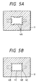
- Figs. 5A and 5B show the arrangement of a fourth embodiment of the present invention.
- Bendable protrusions 4A are provided partly along the inner peripheral sides of rectangular opening 4 of insulating film 3.
- slits 4B are provided at four corners of rectangular opening 4 to make sides 4c bendable along the opening 4.
- protrusions 4a and sides 4c are flexibly bendable when the main body of electronic component 5 is forcibly inserted or engaged into opening 4, so that electronic component 5 can be firmly held at its side surfaces to the opening 4 through protrusions 4a or sides 4c.
- the mounting accuracy in positioning an electronic component at a designated position is increased by ⁇ 0.03mm.
- Table 1 shows the measuring result showing how the configuration of opening 4 gives an effect to the mounting accuracy when an electronic component is forcibly inserted.
- Fig. 6 is a cross-sectional side view showing an illuminating switch unit manufactured by the mounting method for mounting an electronic component on a wiring substrate in accordance with the fifth embodiment.
- reference numerals 10 and 11 represent a pair of an insulating substrate and an insulating film, respectively.
- An insulating layer 12 is uniformly printed on insulating substrate 10 for increasing adhesion of insulating substrate 10.
- Simultaneously printed on insulating layer 12 are a stationary contact 14 constituting part of a switch 13 and a conductive pattern 17 for a light emitting device (LED) 16 of an illumination 15.
- LED light emitting device
- Insulating film 11 made of a resilient member, is provided with a diaphragm 18 at a portion opposed to stationary contact 14 of switch 13.
- This diaphragm 18 is formed into a dome shape by squeezing finish, so as to be collapsible.
- a conductive layer 19, serving as a movable contact, is attached on the lower surface of diaphragm 18.
- An opening 20 is provided on insulating film 11 at a position where terminals 16A of LED 16 are brought into contact with conductive pattern 17 of illumination 15. The main body of LED 16 is forcibly entered or engaged into this opening 20.
- Squeezing finish for forming diaphragm 18 of switch 13 and punching for providing opening 20 of illumination 15 can be performed by sequential press working using the same dies.
- an insulating layer 21 is printed partly on the lower surface of insulating film 11 at a region surrounding diaphragm 18 of switch 13 and at a region surrounding terminals 16A of LED 16 of illumination 15. This insulating layer 21 increases the adhesion to insulating layer 12 on insulating substrate 10. Insulating film 11 is welded in the region surrounding terminals 16A of LED 16.
- the above-described arrangement for the illuminating switch unit makes it possible to simultaneously forming switch 13 and illumination 15 on the same insulating substrate 10 and insulating film 11. Hence, downsizing of a switch unit as well as high densification can be realized, while reducing manufacturing costs.
- the present invention makes it possible to easily mount an electronic component on a printed FPC which does not accept the soldering operation, without requiring an expensive mounting machine conventionally used.
- the mounting procedure can be simplified. A higher mounting accuracy can be assured even if a terminal of an electronic component is undesirably short.
- the reliability in electric conductivity is enhanced, and the fixing strength can be increased. Accordingly, it becomes possible to provide an excellent method of mounting an electronic component on a wiring substrate and also it becomes possible to provide an illuminating switch unit manufactured in accordance with this mounting method.
Applications Claiming Priority (3)
| Application Number | Priority Date | Filing Date | Title |
|---|---|---|---|
| JP13908595 | 1995-06-06 | ||
| JP7139085A JPH08335761A (ja) | 1995-06-06 | 1995-06-06 | 電子部品の配線基板への装着方法およびこれを用いた照光式スイッチユニット |
| JP139085/95 | 1995-06-06 |
Publications (3)
| Publication Number | Publication Date |
|---|---|
| EP0748152A2 true EP0748152A2 (de) | 1996-12-11 |
| EP0748152A3 EP0748152A3 (de) | 1998-02-25 |
| EP0748152B1 EP0748152B1 (de) | 2002-12-04 |
Family
ID=15237144
Family Applications (1)
| Application Number | Title | Priority Date | Filing Date |
|---|---|---|---|
| EP96304049A Expired - Lifetime EP0748152B1 (de) | 1995-06-06 | 1996-06-04 | Verfahren zum Montieren eines elektronischen Bauteils auf einem Leitersubstrat und elektronische Vorrichtung unter Verwendung dieses Montierungsverfahrens |
Country Status (4)
| Country | Link |
|---|---|
| US (1) | US5848462A (de) |
| EP (1) | EP0748152B1 (de) |
| JP (1) | JPH08335761A (de) |
| DE (1) | DE69625127T2 (de) |
Cited By (5)
| Publication number | Priority date | Publication date | Assignee | Title |
|---|---|---|---|---|
| EP0802710A2 (de) * | 1996-04-17 | 1997-10-22 | Lucent Technologies Inc. | Schutzvorrichtung von elektronischen Schaltkreisen und Baugruppen, die ein metallisiertes biegsames Gehäuse verwenden |
| DE19708325A1 (de) * | 1997-03-03 | 1998-09-10 | Manfred Dr Michalk | Klebeverbindung von elektrisch leitenden Fügeteilen |
| WO2006045258A1 (de) * | 2004-10-26 | 2006-05-04 | Alcan Technology & Management Ltd. | Bandförmige anordnung mit einer leiterbahnstruktur und mit damit elektrisch verbundenen elektronischen bauteilen, insbesondere lichtband mit leuchtelementen |
| EP1863049A3 (de) * | 2006-03-29 | 2009-04-22 | EATON Corporation | Abschirmung und Leiterplatte und elektrische Vorrichtung damit |
| EP3334258A1 (de) * | 2016-12-07 | 2018-06-13 | Kabushiki Kaisha Toshiba | Leiterplattenvorrichtung |
Families Citing this family (9)
| Publication number | Priority date | Publication date | Assignee | Title |
|---|---|---|---|---|
| JPH10244791A (ja) * | 1997-03-07 | 1998-09-14 | Fujitsu Ltd | カード型電子装置 |
| JP2000208905A (ja) * | 1999-01-14 | 2000-07-28 | Nec Corp | プリント基板 |
| JP2001345549A (ja) * | 2000-06-01 | 2001-12-14 | Fujitsu Ltd | 実装用基板の製造方法及び部品実装方法並びに実装用基板製造装置 |
| US7083311B2 (en) * | 2002-01-12 | 2006-08-01 | Schefenacker Vision Systems Germany Gmbh & Co. Kg | Conductor of flexible material, component comprising such flexible conductor, and method of manufacturing such conductor |
| US7690812B2 (en) * | 2007-03-16 | 2010-04-06 | Cree, Inc. | Apparatus and methods for conformable diffuse reflectors for solid state lighting devices |
| US10429929B2 (en) | 2010-09-24 | 2019-10-01 | Blackberry Limited | Piezoelectric actuator apparatus and methods |
| FR2967308A1 (fr) * | 2010-11-06 | 2012-05-11 | Johnson Controls Tech Co | Dispositif de raccordement electrique flexible entre un composant electrique et une carte imprimee, systeme, et procede de montage d'un systeme. |
| JP2016162905A (ja) * | 2015-03-03 | 2016-09-05 | 株式会社東海理化電機製作所 | リード接続構造 |
| EP3573434A1 (de) * | 2018-05-25 | 2019-11-27 | Nederlandse Organisatie voor toegepast- natuurwetenschappelijk onderzoek TNO | Dehnbare elektronische vorrichtung |
Citations (7)
| Publication number | Priority date | Publication date | Assignee | Title |
|---|---|---|---|---|
| US4320272A (en) * | 1981-01-26 | 1982-03-16 | Oak Industries Inc. | Connector for attaching an electrical component to a flat sheet |
| US4442938A (en) * | 1983-03-22 | 1984-04-17 | Advanced Interconnections | Socket terminal positioning method and construction |
| GB2186427A (en) * | 1986-02-12 | 1987-08-12 | Shinetsu Polymer Co | Mounting electronic devices |
| EP0345427A2 (de) * | 1988-06-04 | 1989-12-13 | Hagenuk Gmbh | Schaltungsträger für elektrische Bauelemente als Schaltfolien, Platinen oder dergleichen |
| EP0347974A2 (de) * | 1988-06-23 | 1989-12-27 | Teikoku Tsushin Kogyo Co. Ltd. | Montage von elektronischen Bauteilen |
| NL8801448A (nl) * | 1988-06-06 | 1990-01-02 | Docdata Bv | Werkwijze voor het assembleren van printkaarten. |
| DE4303743A1 (de) * | 1992-02-10 | 1993-08-12 | Matsushita Electric Ind Co Ltd |
Family Cites Families (13)
| Publication number | Priority date | Publication date | Assignee | Title |
|---|---|---|---|---|
| JPS55138291A (en) * | 1979-04-11 | 1980-10-28 | Alps Electric Co Ltd | Substrate for mounting electric parts |
| US4365408A (en) * | 1980-07-24 | 1982-12-28 | Re-Al, Inc. | Method of making membrane contact switch |
| JPS63158711A (ja) * | 1986-12-22 | 1988-07-01 | 帝国通信工業株式会社 | フレキシブルプリント基板の端子構造 |
| US4772769A (en) * | 1987-02-06 | 1988-09-20 | Burr-Brown Corporation | Apparatus for selective backlighting of keys of a keyboard |
| US4967261A (en) * | 1987-07-30 | 1990-10-30 | Mitsubishi Denki Kabushiki Kaisha | Tape carrier for assembling an IC chip on a substrate |
| JPH0760926B2 (ja) * | 1988-09-14 | 1995-06-28 | 帝国通信工業株式会社 | 電子部品実装体 |
| JPH0338088A (ja) * | 1989-07-05 | 1991-02-19 | Jieruko:Kk | フレキシブル印刷配線板における電子部品の接続固定方法 |
| JP2753746B2 (ja) * | 1989-11-06 | 1998-05-20 | 日本メクトロン株式会社 | Ic搭載用可撓性回路基板及びその製造法 |
| US5331513A (en) * | 1991-07-12 | 1994-07-19 | Rohm Co., Ltd. | Method of mounting electronic part on circuit substrate and circuit substrate including electronic parts mounted thereon |
| JP2767670B2 (ja) * | 1992-09-03 | 1998-06-18 | 株式会社村田製作所 | 電子部品チップ用ホルダおよびそれを用いた電子部品チップの電極形成方法 |
| JPH06310839A (ja) * | 1993-04-27 | 1994-11-04 | Matsushita Electric Ind Co Ltd | フレキシブル印刷回路板への電子部品の実装方法 |
| JPH0831679B2 (ja) * | 1993-06-18 | 1996-03-27 | 帝国通信工業株式会社 | フレキシブル基板への電子部品の取付構造及びその取付方法 |
| JP3038088U (ja) | 1996-11-21 | 1997-06-06 | 株式会社拓殖商事 | 穀物用袋 |
-
1995
- 1995-06-06 JP JP7139085A patent/JPH08335761A/ja active Pending
-
1996
- 1996-05-31 US US08/655,931 patent/US5848462A/en not_active Expired - Fee Related
- 1996-06-04 DE DE69625127T patent/DE69625127T2/de not_active Expired - Fee Related
- 1996-06-04 EP EP96304049A patent/EP0748152B1/de not_active Expired - Lifetime
Patent Citations (7)
| Publication number | Priority date | Publication date | Assignee | Title |
|---|---|---|---|---|
| US4320272A (en) * | 1981-01-26 | 1982-03-16 | Oak Industries Inc. | Connector for attaching an electrical component to a flat sheet |
| US4442938A (en) * | 1983-03-22 | 1984-04-17 | Advanced Interconnections | Socket terminal positioning method and construction |
| GB2186427A (en) * | 1986-02-12 | 1987-08-12 | Shinetsu Polymer Co | Mounting electronic devices |
| EP0345427A2 (de) * | 1988-06-04 | 1989-12-13 | Hagenuk Gmbh | Schaltungsträger für elektrische Bauelemente als Schaltfolien, Platinen oder dergleichen |
| NL8801448A (nl) * | 1988-06-06 | 1990-01-02 | Docdata Bv | Werkwijze voor het assembleren van printkaarten. |
| EP0347974A2 (de) * | 1988-06-23 | 1989-12-27 | Teikoku Tsushin Kogyo Co. Ltd. | Montage von elektronischen Bauteilen |
| DE4303743A1 (de) * | 1992-02-10 | 1993-08-12 | Matsushita Electric Ind Co Ltd |
Non-Patent Citations (2)
| Title |
|---|
| PATENT ABSTRACTS OF JAPAN vol. 15, no. 170 (E-1062), 30 April 1991 & JP 03 038088 A (JIERUKO KK), 19 February 1991, * |
| PATENT ABSTRACTS OF JAPAN vol. 95, no. 4, 31 May 1995 & JP 07 007249 A (TEIKOKU TSUSHIN KOGYO CO), 10 January 1995, * |
Cited By (7)
| Publication number | Priority date | Publication date | Assignee | Title |
|---|---|---|---|---|
| EP0802710A2 (de) * | 1996-04-17 | 1997-10-22 | Lucent Technologies Inc. | Schutzvorrichtung von elektronischen Schaltkreisen und Baugruppen, die ein metallisiertes biegsames Gehäuse verwenden |
| EP0802710A3 (de) * | 1996-04-17 | 1998-04-22 | Lucent Technologies Inc. | Schutzvorrichtung von elektronischen Schaltkreisen und Baugruppen, die ein metallisiertes biegsames Gehäuse verwenden |
| DE19708325A1 (de) * | 1997-03-03 | 1998-09-10 | Manfred Dr Michalk | Klebeverbindung von elektrisch leitenden Fügeteilen |
| DE19708325B4 (de) * | 1997-03-03 | 2007-06-14 | Sokymat Gmbh | Klebeverbindung von elektrisch leitenden Fügeteilen |
| WO2006045258A1 (de) * | 2004-10-26 | 2006-05-04 | Alcan Technology & Management Ltd. | Bandförmige anordnung mit einer leiterbahnstruktur und mit damit elektrisch verbundenen elektronischen bauteilen, insbesondere lichtband mit leuchtelementen |
| EP1863049A3 (de) * | 2006-03-29 | 2009-04-22 | EATON Corporation | Abschirmung und Leiterplatte und elektrische Vorrichtung damit |
| EP3334258A1 (de) * | 2016-12-07 | 2018-06-13 | Kabushiki Kaisha Toshiba | Leiterplattenvorrichtung |
Also Published As
| Publication number | Publication date |
|---|---|
| EP0748152A3 (de) | 1998-02-25 |
| US5848462A (en) | 1998-12-15 |
| DE69625127D1 (de) | 2003-01-16 |
| EP0748152B1 (de) | 2002-12-04 |
| DE69625127T2 (de) | 2003-05-08 |
| JPH08335761A (ja) | 1996-12-17 |
Similar Documents
| Publication | Publication Date | Title |
|---|---|---|
| EP0272707A2 (de) | Anordnung von End-Verbindern an flexiblen gedruckten Schaltungen | |
| US5805251A (en) | Noise-shield sheet and liquid crystal display device using the same | |
| EP0748152A2 (de) | Verfahren zum Montieren eines elektronischen Bauteils auf einem Leitersubstrat und beleuchteter Schalter unter Verwendung dieses Montierungsverfahrens | |
| US7122745B2 (en) | Circuit board having metallic plate, printed circuit board and flexible circuit board | |
| US5216358A (en) | Device for testing a printed circuit board | |
| GB2169750A (en) | Flexible cable assembly | |
| JP3424272B2 (ja) | 配線回路基板接続用フレキシブル基板 | |
| US5444299A (en) | Electronic package with lead wire connections | |
| JP2973293B2 (ja) | フレキシブルプリント基板の端子構造及び該端子構造の製造方法 | |
| JP2601580B2 (ja) | 可撓性プリント基板の両面実装方法 | |
| JPH07162120A (ja) | フレキシブルプリント配線板の回路接続方法及びフレキシブルプリント配線板 | |
| JPH1093229A (ja) | 電子部品の配線基板への装着方法およびこれを用いた照光式スイッチユニット | |
| JPH1145U (ja) | プッシュスイッチ | |
| JPH0523367U (ja) | プツシユスイツチ | |
| JPH09331143A (ja) | フレキシブル配線基板への電子部品装着方法 | |
| JPH10284809A (ja) | 回路モジュール及びその製造方法 | |
| JPH08249932A (ja) | フラット・ハーネス | |
| JPH071817Y2 (ja) | 半導体集積回路実装機構 | |
| JP3110329B2 (ja) | 電子部品の半田付け方法 | |
| JPH09199242A (ja) | プリント配線板一体型コネクタ及びその製造方法 | |
| JPH05270186A (ja) | Icカード | |
| JPH0513905A (ja) | 可撓性を有する配線部材 | |
| JPH0997954A (ja) | フレキシブルプリント配線板 | |
| JPH08227633A (ja) | プッシュスイッチとその製造方法 | |
| JPH0710969U (ja) | プリント基板 |
Legal Events
| Date | Code | Title | Description |
|---|---|---|---|
| PUAI | Public reference made under article 153(3) epc to a published international application that has entered the european phase |
Free format text: ORIGINAL CODE: 0009012 |
|
| 17P | Request for examination filed |
Effective date: 19960615 |
|
| AK | Designated contracting states |
Kind code of ref document: A2 Designated state(s): DE FR GB |
|
| PUAL | Search report despatched |
Free format text: ORIGINAL CODE: 0009013 |
|
| AK | Designated contracting states |
Kind code of ref document: A3 Designated state(s): DE FR GB |
|
| 17Q | First examination report despatched |
Effective date: 20001222 |
|
| RTI1 | Title (correction) |
Free format text: METHOD FOR MOUNTING AN ELECTRONIC COMPONENT ON A WIRING SUBSTRATE AND AN ELECTRONIC DEVICE USING THIS MOUNTING METHOD |
|
| GRAG | Despatch of communication of intention to grant |
Free format text: ORIGINAL CODE: EPIDOS AGRA |
|
| GRAG | Despatch of communication of intention to grant |
Free format text: ORIGINAL CODE: EPIDOS AGRA |
|
| GRAH | Despatch of communication of intention to grant a patent |
Free format text: ORIGINAL CODE: EPIDOS IGRA |
|
| GRAH | Despatch of communication of intention to grant a patent |
Free format text: ORIGINAL CODE: EPIDOS IGRA |
|
| GRAA | (expected) grant |
Free format text: ORIGINAL CODE: 0009210 |
|
| AK | Designated contracting states |
Kind code of ref document: B1 Designated state(s): DE FR GB |
|
| REG | Reference to a national code |
Ref country code: GB Ref legal event code: FG4D |
|
| REF | Corresponds to: |
Ref document number: 69625127 Country of ref document: DE Date of ref document: 20030116 |
|
| ET | Fr: translation filed | ||
| PLBE | No opposition filed within time limit |
Free format text: ORIGINAL CODE: 0009261 |
|
| STAA | Information on the status of an ep patent application or granted ep patent |
Free format text: STATUS: NO OPPOSITION FILED WITHIN TIME LIMIT |
|
| 26N | No opposition filed |
Effective date: 20030905 |
|
| PGFP | Annual fee paid to national office [announced via postgrant information from national office to epo] |
Ref country code: GB Payment date: 20060809 Year of fee payment: 11 |
|
| PGFP | Annual fee paid to national office [announced via postgrant information from national office to epo] |
Ref country code: FR Payment date: 20060825 Year of fee payment: 11 |
|
| PGFP | Annual fee paid to national office [announced via postgrant information from national office to epo] |
Ref country code: DE Payment date: 20070531 Year of fee payment: 12 |
|
| GBPC | Gb: european patent ceased through non-payment of renewal fee |
Effective date: 20070604 |
|
| REG | Reference to a national code |
Ref country code: FR Ref legal event code: ST Effective date: 20080229 |
|
| PG25 | Lapsed in a contracting state [announced via postgrant information from national office to epo] |
Ref country code: GB Free format text: LAPSE BECAUSE OF NON-PAYMENT OF DUE FEES Effective date: 20070604 |
|
| PG25 | Lapsed in a contracting state [announced via postgrant information from national office to epo] |
Ref country code: FR Free format text: LAPSE BECAUSE OF NON-PAYMENT OF DUE FEES Effective date: 20070702 |
|
| PG25 | Lapsed in a contracting state [announced via postgrant information from national office to epo] |
Ref country code: DE Free format text: LAPSE BECAUSE OF NON-PAYMENT OF DUE FEES Effective date: 20090101 |