EP0735352B1 - Transducteur de force et son procédé de fabrication - Google Patents
Transducteur de force et son procédé de fabrication Download PDFInfo
- Publication number
- EP0735352B1 EP0735352B1 EP96105141A EP96105141A EP0735352B1 EP 0735352 B1 EP0735352 B1 EP 0735352B1 EP 96105141 A EP96105141 A EP 96105141A EP 96105141 A EP96105141 A EP 96105141A EP 0735352 B1 EP0735352 B1 EP 0735352B1
- Authority
- EP
- European Patent Office
- Prior art keywords
- strain gages
- force transducer
- single crystal
- silicon single
- crystal substrate
- Prior art date
- Legal status (The legal status is an assumption and is not a legal conclusion. Google has not performed a legal analysis and makes no representation as to the accuracy of the status listed.)
- Expired - Lifetime
Links
Images


Classifications
-
- G—PHYSICS
- G01—MEASURING; TESTING
- G01L—MEASURING FORCE, STRESS, TORQUE, WORK, MECHANICAL POWER, MECHANICAL EFFICIENCY, OR FLUID PRESSURE
- G01L1/00—Measuring force or stress, in general
- G01L1/18—Measuring force or stress, in general using properties of piezo-resistive materials, i.e. materials of which the ohmic resistance varies according to changes in magnitude or direction of force applied to the material
Definitions
- This invention relates to a force transducer that converts a compression force into an electrical signal, and, in particular, to a force transducer that makes use of the piezoresistive effect of a semiconductor.
- a force transducer When a force transducer is used for measuring combustion pressures within a cylinder of an engine, that force transducer is required to have a high compression fracture strength and a high output level, in order to enable accurate control over the engine.
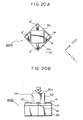
- FIGs. 20A and 20B An example of a force transducer (taken from US-A 4,833,929) is shown in Figs. 20A and 20B, where Fig. 20A is a plan view and Fig. 20B is a cross-sectional view thereof.
- This force transducer comprises a rectangular p-type silicon semiconductor 10 having a (110) crystal face 10a to which a compression force W is applied, a pressure transfer block 30 connected to the crystal face 10a of the silicon semiconductor 10 and transferring the compression force (indicated by W in the figure) perpendicularly to the crystal face 10a, and a support base 20.
- the silicon semiconductor 10 is also provided with a pair of input electrodes 14 and 14' that oppose one another in a direction at 45° counterclockwise from the ⁇ 110> crystal direction of the silicon semiconductor 10, and a current flows through the silicon semiconductor 10 between these input electrodes 14 and 14'.
- Another pair of electrodes 12 and 12' are provided on the silicon semiconductor 10, opposing one another in a direction at 45° counterclockwise from the ⁇ 001> crystal direction.
- a voltage corresponding to the compression force W is output from the pair of electrodes 12 and 12', due to the piezoresistive effect of the silicon semiconductor.
- the piezoresistive coefficient ⁇ 63 is expressed by Formula (2) below. For more details, refer to "Use of Piezoresistive Materials in the Measurement of Displacement, Force, and Torque," The Journal of the Acoustical Society of America, Vol. 29, No. 10, Oct. 1957. If p-type silicon having a resistivity of approximately 8 ⁇ •cm is used, for example, the piezoresistive coefficient ⁇ 63 will be approximately 33 x 10 -6 cm 2 /kg. ⁇ 63 ⁇ 1 4 ( ⁇ 11 - ⁇ 12 - ⁇ 44 )
- ⁇ 11 , ⁇ 12 , and ⁇ 44 are the piezoresistive coefficients of a cubic crystal.
- ⁇ 11 6 x 10 -6 cm 2 /kg
- ⁇ 12 -1 x 10 -6 cm 2 /kg
- ⁇ 44 138 x 10 -6 cm 2 /kg.
- the present inventors have performed further research based on the above described technology of force transducers, and, as a result, have determined the following problems with this technology: 1.
- an effective method of applying temperature compensation to the output of the force transducer is to ensure that the input resistance of the force transducer has a temperature characteristic that is the inverse of that of the detection output, to cancel any change in the characteristics of the detection output.
- a beneficial temperature characteristic for the resistance it is necessary to use high-density doping of an impurity into the semiconductor single crystal that constitutes the force transducer.
- GB-A-2 207 804 discloses a force transducer in accordance with the first part of claim 1. Protruding strain gages are formed on a silicon single crystal substrate via an oxide layer. A pressure transfer block is acting on the diaphragm part of the substrate, for producing strain transmitted to the strain gages.
- DE-A-44 19 138 discloses a force transducer comprising a deflection sensing portion in the form of a Wheatstone bridge of piezoresistances which is connected to a plurality of rods so as to form strain gages on a crystal face of a silicon single crystal.
- the resistances of the strain gages are changed when a compression force is applied to them via a pressure transfer member consisting of a rod and mushroom-shaped member located above the strain gages.
- WO-A-92/15851 is directed to a pressure sensor wherein the force is introduced into a piezoresistive measuring element via a membrane and a plunger.
- the piezoresistive measuring element is part of silicon single crystal chip and is connected thereto in the form of a Wheatstone bridge circuit which may comprise two pairs of opposing resistances.
- US-A-4 454 771 is directed to a load cell which comprises a semiconductor diaphragm including a membrane wherein at least two piezoresistors forming part of a bridge circuit are formed.
- the principal surface of the silicon wafer forming the membrane extends in the ⁇ 110 ⁇ -plane.
- An objective of the present invention is to provide a force transducer having high compression fracture strength and high detection sensitivity, thus satisfying both detection precision and reliability.
- the invention also provides a method of fabricating such a force transducer.
- a force transducer of present invention is defined in claim 1.
- the force transducer in accordance with this invention is preferably configured in such a manner that a compression force of a pressure transfer block acts on narrow strain gages protruding from a surface of a silicon substrate.
- This configuration differs from that of a conventional force transducer in which the compression force acts on a single crystal surface, in that the area on which the pressure acts is much smaller, and thus a large compression strain is generated in the strain gages, increasing the detection sensitivity.
- This configuration may use the piezoresistive coefficient ⁇ 13 , which has a sensitivity that is at a maximum in the ⁇ 110> direction of the (110) surface of silicon single crystal, thus enabling the use of a novel configuration of the standard bridge construction.
- This invention is further characterized in that the amount of protuberance of the strain gages (their height of protrusion) is preferably such that, if the compression force exceeds a predetermined value, the deformation caused by that compression force will bring part of the pressure transfer block into contact with the surface of the silicon crystal.
- a silicon single crystal doped with a high density of an impurity is preferably used in the force transducer of the present invention. This makes it possible to suppress any change in characteristics of the force transducer due to changes in temperature. Since narrow, protuberant strain gages are used in the force transducer of this invention, their cross-sectional area is small and thus the resistance of these strain gages can be increased. Therefore, it is possible to guarantee an input resistance of approximately 1 k ⁇ as the resistance of these strain gages, despite the above described problems caused by a high impurity density in a silicon single crystal, and thus it is possible to fabricate strain gages that are sufficiently sturdy for practical use.
- the force transducer of this invention is also preferably provided with "guard banks" on either side of the strain gages. These guard banks are formed to protrude from the surface of the silicon single crystal to the same degree as the strain gages and are electrically insulated therefrom.
- the guard banks always bear the compression forces, and they also bear any horizontal component of force that might be generated by deformation of the pressure transfer block by the compression forces, so that they function to reduce such horizontal components of force acting on the strain gages. This further improves the fracture strength of the force transducer.
- narrow, protuberant strain gages are preferably formed by batch mesa etching of a semiconductor substrate. This enables protuberant strain gages to be formed by a simple process.
- the method of fabricating a force transducer in accordance with this invention preferably uses a silicon-on-insulator (SOI) substrate. This makes it possible to form strain gages that can be used at high temperatures of 200°C or above, by a simple process.
- SOI silicon-on-insulator
- the present invention makes it possible to fabricate a force transducer which has a high reliability and also a sensitivity eight times as high as that of a conventional force transducer. Therefore it is likely that there will be no need to provide an amplifier to amplify the sensor output when the sensor is used in a combustion pressure sensor. If an amplifier occupying approximately 1/3 the price of the entire sensor can be omitted, it will be easier to reduce the cost of the combustion pressure sensor.
- Table 1 shows the crystal faces equivalent to the crystal face of (110) and the directions of crystallization equivalent to the directions of [001] and [ 110 ], respectively, of the Si single crystal.
- a crystal face equivalent to the crystal face of (110) is represented by ⁇ 110 ⁇ and the directions equivalent to the directions of [001] and [ 110 ] are represented by ⁇ 001> and ⁇ 110>, respectively.
- Crystal face Direction of crystallization Direction of crystallization (110) [001] [1 1 0] ( 11 0) [001] [1 1 0] (1 1 0) [001] [110] ( 1 10) [001] [110] (101) [010] [10 1 ] ( 1 0 1 ) [010] [10 1 ] (10 1 ) [010] [101] ( 1 01) [010] [101] (011) [100] [0 11 ] (0 11 ) [100] [01 1 ] (01 1 ) [100] [011] (0 1 1) [100] [011]
- a force transducer 1000 in accordance with a first embodiment of this invention is shown in perspective view in Fig. 1.
- the force transducer 1000 comprises a block of silicon single crystal 40 with a (110) surface, a pressure transfer block 60 made of crystallized glass, and a base 70, all of these components being fixed together by electrostatic bonding.
- the silicon single crystal 40 with a (110) crystal face is an n-type semiconductor with a resistivity of approximately 1 ⁇ -cm.
- This silicon single crystal 40 is machined into a rectangular block with a width of 1.4 mm, a length of 2.0 mm, and a height of 0.3 mm.
- the base 70 is similarly machined into a rectangular block with a width of 1.4 mm, a length of 2.0 mm, and a height of 0.5 mm.
- strain gages Ga1, Ga2, Gb1, and Gb2 with a width of 10 ⁇ m are formed in a full-bridge configuration on the surface of the silicon single crystal on the side of the junction between the silicon single crystal 40 and the pressure transfer block 60.
- strain gages could be formed by diffusing boron over the entire surface of an n-type semiconductor to form 0.001 ⁇ -cm p-type semiconductor layer (reference number 41 in Figs.3A and 3B), then etching this semiconductor surface to a depth of 3 ⁇ m.
- the pressure transfer block 60 is a rectangular block of crystallized glass attached to the strain gages Ga1, Ga2, Gb1, and Gb2 by electrostatic bonding, with a width of 1.0 mm, a length of 1.0 mm, and a height of 0.5 mm. A compression force W that is applied to the upper surface thereof is transferred perpendicularly to the strain gages Ga1, Ga2, Gb1, and Gb2.
- the longitudinal direction of one pair of mutually opposing strain gages Ga1 and Ga2 is aligned with the ⁇ 110> direction of the crystal, and the longitudinal direction of the other pair of mutually opposing strain gages Gb1 and Gb2 is aligned with the ⁇ 100> direction of the crystal, as shown in Fig. 2.
- Leads 43a to 43d protrude from the connecting portions between adjacent strain gages, and the leads 43a to 43d are connected to electrodes 44b2, 44a2, 44a1, and 44b1, respectively.
- the leads 43a to 43d are formed of the same p-type semiconductor as the strain gages Ga1, Ga2, Gb1, and Gb2.
- the electrodes 44a1, 44a2, 44b1, and 44b2 have a thickness of approximately 1 ⁇ m.
- Reference numbers 44a1 and 44a2 denote input electrodes
- reference numbers 44b1 and 44b2 denote output electrodes. If a constant current is supplied to the input electrodes, a voltage output (V) that is proportional to the compression force W acting on the pressure transfer block 60, is obtained from the output electrodes.
- V voltage output
- the relationship between the voltage output V, and the compression force W and the piezoresistive coefficient ⁇ 13 is as follows:
- ⁇ 13 1 2 ( ⁇ 11 + ⁇ 12 - ⁇ 14 ) where: ⁇ 12 ⁇ ( ⁇ 11 - ⁇ 44 )
- Sensitivity of the piezoresistive coefficient ⁇ 13 is plotted in polar coordinates in Fig. 19.
- suitable semiconductors where the piezoresistive coefficient ⁇ 13 can be used effectively are the (111) or (211) surface of a p-type semiconductor or the (111) or (211) surface of an n-type semiconductor.
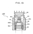
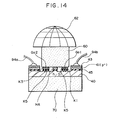
- a combustion pressure sensor 1100 in which the force transducer 1000 of this embodiment is used as a pressure detection means is shown.
- This combustion pressure sensor 1100 comprises a cylindrical housing 80 provided with a metal diaphragm 82, and the force transducer 1000 fixed within this housing 80.
- the housing 80 is attached to a wall surface of an engine cylinder head (not shown in the figure) and is formed in such a manner that the pressure P within the cylinder acts on the metal diaphragm 82.
- the force transducer 1000 is fixed within the housing 80 by a sealed terminal 90, and a top portion 62 of the pressure transfer block 60 is formed in a dome shape and is in contact with the rear surface of the metal diaphragm 82.
- This configuration ensures that the pressure P within the cylinder is converted into the compression force W by the metal diaphragm 82, this compression force W is transferred to the top portion 62 of the pressure transfer block 60 constituting the force transducer 1000, then finally acts as compression strains in the (110) crystal face of the silicon semiconductor shown in Fig. 1.
- the sealed terminal 90 is provided with lead pins 92a, 92b, 92c, and 92d (note that only 92a and 92b are shown in Fig. 13). These lead pins 92a, 92b, 92c, and 92d are electrically connected to the electrodes 44a1, 44a2, 44b1, 44b2 of the force transducer 1000 by bonding wires 94a, 94b, etc., of a diameter of 50 ⁇ m.
- the configuration of this embodiment uses the piezoresistive coefficient ⁇ 13 that has a maximum sensitivity in the ⁇ 110> direction on the (110) surface of a silicon single crystal, to make it possible to implement the use of a novel configuration that forms a bridge.
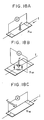
- the piezoresistive coefficient ⁇ 13 refers to the piezoresistive coefficient used when the voltage-detection direction and the current-flow direction are the same, and a uniaxial stress acts in a direction perpendicular thereto, as shown in Fig. 18A.
- the piezoresistive coefficient ⁇ 63 used in the conventional configuration refers to the piezoresistive coefficient used when the voltage-detection direction and current-flow direction cross, and a uniaxial stress acts in a direction perpendicular to both of these directions, as shown in Fig. 18B.
- the piezoresistive coefficient ⁇ 12 is the piezoresistive coefficient used when the voltage-detection direction and the current-flow direction are the same, and a uniaxial stress acts in the horizontal direction perpendicular thereto, as shown in Fig. 18C.
- the piezoresistive coefficient ⁇ 13 has a sensitivity that is at a maximum in the ⁇ 110> direction on the (110) surface, but is zero in the ⁇ 100> direction, as shown in Fig.19. Therefore, if strain gages are disposed in the directions to form a Wheatstone bridge, an output that is equivalent to that of a half bridge can be obtained with a full-bridge configuration.
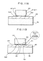
- a characteristic feature of this embodiment is that the strain gages are formed as narrow strain gages protruding from the semiconductor substrate as shown in Fig. 3A. Note that only two strain gages Ga1 and Ga2 are shown in this figure.
- This configuration ensures that the pressure-bearing area of the strain gages is markedly smaller than in conventional configurations in which the compression force acts over the entire surface of the substrate, so that a larger compression strain acts on each strain gage, increasing the detection sensitivity.
- the detection output of this force transducer is proportional to the product of the piezoresistive coefficient and the stress. Therefore, an effective way of increasing the stress acting on the detector portion is to reduce the pressure-bearing area of the detector portion.
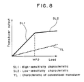
- Another characteristic feature of this embodiment is that the height of protrusion of the strain gages can be adjusted to ensure that, when the load exceeds a predetermined value, stopper regions STP1 to STP4 come into mutual contact as shown in Fig. 3B to act as stoppers and thus distribute the compression force W.
- the action of these stoppers distributes the compression force acting on the narrow, three-dimensional strain gages, thus improving their fracture strength.
- the height of protrusion of the strain gages is preferably between 1 ⁇ m and 3 ⁇ m.
- part of the lower surface of the pressure transfer block 60 and part of the surface of the n-type silicon substrate act as the above described stopper region.
- a high-sensitivity characteristic S1 is the characteristic obtained when the stopper is not operated, and a low-sensitivity characteristic S2 is that obtained when the stopper is operated.
- WP1 the load at which the stopper starts to act
- a curve D1 is the characteristic in accordance with this embodiment.
- a further characteristic feature of this embodiment is a configuration in which four strain gages Ga1, Ga2, Gb1, and Gb2 are disposed to form the sides of a quadrangle in a plane, as shown in Fig. 2, and the compression strain of the pressure transfer block 60 acts on each of these strain gages.
- a still further characteristic feature of this embodiment is that force transfer provides its own temperature compensation and resistance to high temperatures by using the advantages of narrow strain gages arranged in a grid formation.
- a high density of a p-type impurity is diffused into a top portion of each of the strain gages Ga1, Ga2, Gb1, and Gb2, which directly bears the compression force acting on that strain gages, as shown in Fig. 15B.
- This impurity density is a density of the order of a point A or a point B in Fig. 17B, which enables automatic compensation of the temperature characteristic of the sensor output. Since the cross-sectional area of each of the strain gages is small in this embodiment, an input resistance of approximately 1 k ⁇ can be guaranteed, even with such a high impurity density, to provide strain gages that can cope with practical usage.
- this force transducer can be used at temperatures of at least approximately 200°C.
- Fig. 17A While a constant voltage is being applied, the sensor sensitivity G and the resistance R of the strain gages vary with temperature T, as shown for example in Fig. 17A.
- the example shown in Fig. 17A relates to temperature characteristics G1 and R1.
- Impurity densities that enable this temperature compensation are in the vicinity of 1 x 10 18 atoms/cm 3 (point A) and 1 x 10 20 atoms/cm 3 (point B) for the p-type semiconductor as illustrated in Fig. 17B, and use of these impurity densities can greatly improve the dependency on temperature of the sensitivity.
- the present invention uses narrow, protuberant strain gages, the cross-sectional area thereof is small and thus the resistance of these strain gages has been increased. Therefore, an input resistance of approximately 1 k ⁇ can be guaranteed, even with such a high impurity density, to enable the fabrication of strain gages that can cope with practical usage.
- the force transducer of the present invention can be improved in resistance to high temperatures, as described below.
- a pn junction is inevitably formed when a strain gage is formed on the surface of an n-type semiconductor substrate and a p-type impurity is diffused therein to provide the above described temperature compensation. Since the leakage current at such a pn junction increases as the ambient temperature increases, this is a cause of worsening of the temperature characteristic.
- the forming of deep steps by etching ensures that such pn junctions occur only within the strain gages portions of the force transducer. This ensures that leakage currents are reduced, in comparison with a configuration in which a p-type layer is formed uniformly over the surface of the semiconductor substrate, and thus provides a force transducer that can resist higher temperatures.
- This force transducer can be used at temperatures of at least 200°C.
- the presence of the insulating layer prevents pn junctions from being formed and thus a force transducer that can withstand higher temperatures is provided.
- FIGs. 7A and 7B A second embodiment of this invention is shown in Figs. 7A and 7B.
- two-stage etching is performed on a surface of an n-type single crystal silicon 40 to form a shallow stepped portion MS1 and a deep stepped portion MS2.
- the substrate surface of the shallow stepped portion MS1 functions in the same manner as the stoppers STP3 and STP4 shown in Figs. 3A and 3B, but the deep stepped portion MS2 does not function as a stopper.
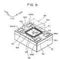
- FIG. 9 The configuration of a third embodiment of this invention is shown in Fig. 9.
- a first characteristic feature of this embodiment is the provision of guard banks K1 to K5.
- this embodiment is provided with guard banks K1 to K5 on each side of the strain gages Ga1, Ga2, Gb1, and Gb2.
- These guard banks have the same properties and shapes as the strain gages, but are separated therefrom by a distance that is between one and five times the width of the strain gages and are not connected electrically thereto. They mitigate in-plane stresses acting on the strain gages, and also mitigate stress concentrations at the shoulder portions of the strain gages.
- each "guard bank” always bears compression forces and also any horizontal components of force that might be generated by deformation of the pressure transfer block by these compression forces. They thus reduce any horizontal components of force acting on the strain gages. Therefore, inplane stresses generated by pressure on the corner portions of the strain gages due to deformation of the pressure transfer block under compression are mitigated by these guard bank portions, which enables an improvement in the action of the effective compression strain on the strain gages. This makes it possible to increase the sensitivity of the force transducer and also improve the fracture strength thereof.
- a second characteristic feature of this embodiment is the provision of a central protuberant portion HA.
- the central protuberant portion always bears compression forces, and mainly acts to restrain deformation of the pressure transfer block. Therefore, change in the pressure-bearing area is kept small and there is no deterioration of the detection sensitivity, making it possible to increase the load at which the pressure transfer block starts to come into contact with the stopper. This expands the high sensitivity region, which is useful for improving design freedom.
- the guard banks K1 to K4 are provided on the outer sides of each of the strain gages Ga1, Gb2, Ga2, and Gb1, respectively, and a single guard bank K5 is provided within the perimeter set by the strain gages Ga1, Gb2, Ga2, and Gb1, as shown in Fig. 10.
- the central protuberant portion HA in the configuration of this embodiment always bears the load of the pressure transfer block 60 and thus controls the deformation thereof.
- the guard banks K1 to K5 bear part of the compression force that is applied to the strain gages, so that the load on the strain gages is less than that in the configuration of Fig. 11A, which further improves the compression resistance shown in Fig. 12.
- This embodiment of the present invention relates to a method of fabricating the above described semiconductor force transducer.
- mesa etching is performed after an impurity has been diffused into the entire surface of a semiconductor substrate, to form strain gages in a grid form. This enables the fabrication of strain gages having the superior characteristics described above, by a simple process.
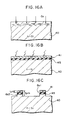
- a p-type impurity is diffused into the entire surface of an n-type silicon single crystal substrate 40 to form a p-type diffusion layer 41 having a thickness of approximately 1 ⁇ m, as shown in Fig. 15A.
- mesa etching to a depth of approximately 3 ⁇ m is performed, except for strain gage portions, lead portions, and electrode portions, to form stopper portions, the strain gages Ga1, Ga2, etc., lead portions, and electrode portions in a single process, as shown in Fig. 15B.
- This fabrication method enables efficient fabrication of the semiconductor force transducer in accordance with this invention that is shown in Fig. 1 or Fig. 9.
- This embodiment enables the fabrication of a semiconductor force transducer that can be used at high temperatures of 200°C or above, by a simple process using a silicon-on-insulator (SOI) substrate.
- SOI silicon-on-insulator
- the means for obtaining the SOI-structure silicon substrate could be an epitaxial growth technique, a technique of directly bonding silicon wafers, or a method using the implantation of oxygen ions (SIMOX method), but the SOI substrate of this embodiment is actually formed by the SIMOX method.
- oxygen ions are implanted from the surface of an n-type silicon semiconductor substrate 40, as shown in Fig. 16A, the oxygen ions are activated by thermal processing, so that an insulating layer (denoted by reference number 45 in Fig. 16B) is formed within the surface of the silicon substrate.
- boron (B) is diffused into the entire surface to form a high-density p-type layer 41, as shown in Fig. 16B.
- the surface of the semiconductor substrate is then subjected to mesa etching to form the strain gages Ga1, Ga2, etc., as shown in Fig. 16C.
- the semiconductor strain gages of the above SOI structure can be used in the assembly shown in Fig. 14.
- a hemispherical head portion 62 is provided at the top of the pressure transfer block 60.
Claims (13)
- Transducteur de force comportant :caractérisé en ce queun substrat (40) en monocristal en silicium, ayant une face de cristal {110} en tant que surface destinée à recevoir une force en compression ;un bloc (60) de transfert de pression, destiné à transférer la force de compression au substrat (40) en monocristal de silicium ; etdes jauges de contrainte (Ga1, Ga2, Gb1, Gb2) disposées sur le substrat (40) en monocristal en silicium ;les jauges de contrainte (Ga1, Ga2, Gb1, Gb2) sont formées de manière à faire saillie de la face de cristal {110} du substrat (40) en monocristal de silicium et pour constituer un circuit de pont constitué de deux paires de jauges de contrainte (Ga1, Ga2, Gb1, Gb2) opposées, la résistance électrique des jauges de contrainte (Ga1, Ga2, Gb1, Gb2) étant dépendante de la force en compression transférée par le bloc (60) de transfert de pression suivant un coefficient de piézo-résistance de π13,le bloc de pression est fixé sur les jauges de contrainte (Ga1, Ga2, Gb1, Gb2) ; etla direction longitudinale d'une paire des jauges de contrainte (Ga1, Ga2, Gb1, Gb2) oppcsées est alignée avec une direction de cristal <110> et la direction longitudinale de l'autre paire des jauges de contrainte (Ga1, Ga2, Gb1, Gb2) opposées est alignée avec une direction de cristal <100>.
- Transducteur de force suivant la revendication 1, dans lequel la hauteur de saillie des jauges de contrainte (Ga1, Ga2, Gb1, Gb2) est telle qu'une partie du bloc (60) de transfert de pression à sa surface de fond vient en contact avec la surface du substrat (40) en cristal en silicium lorsque la force de compression dépasse une valeur déterminée à l'avance et lorsque le bloc (60) de transfert de pression est déformé.
- Transducteur de force suivant la revendication 1, dans lequel une partie partiellement en forme de dent est prévue dans la surface du substrat (40) en monocristal de silicium de telle manière que, lorsque la force de compression dépasse une valeur déterminée à l'avance et que le bloc (60) de transfert de pression est ainsi déformé, le bloc (60) de transfert de pression vient en contact avec uniquement la surface du substrat (40) en monocristal de silicium, sans venir en contact avec une partie de base de la partie en forme de dent.
- Transducteur de force suivant l'une quelconque des revendications 1 à 3, dans lequel les jauges de contrainte (Ga1, Ga2, Gb1, Gb2) sont disposées de manière à constituer des côtés d'un rectangle ayant deux paires de côtés parallèles, les jauges de contrainte (Ga1, Ga2, Gb1, Gb2) étant agencées quelque peu en étant vers l'intérieur à partir des bords extérieurs de la surface inférieure du bloc (60) de transfert de pression.
- Transducteur de force suivant la revendication 4, dans lequel les jauges de contrainte (Ga1, Ga2, Gb1, Gb2) constituent les côtés du rectangle et sont prévues au voisinage d'une région dans laquelle aucune contrainte n'est produite lorsqu'on comprime le bloc (60) de transfert de pression.
- Transducteur de force suivant la revendication 4 ou 5, dans lequel une impureté de type p est diffusée dans au moins une partie de la surface des jauges de contrainte (Ga1, Ga2, Gb1, Gb2) faisant saillie de la surface du substrat (40) en monocristal de silicium.
- Transducteur de force suivant la revendication 6, dans lequel la densité de l'impureté de type p est une densité de l'ordre de grandeur de 1 x 10¹⁸ atomes/cm3 et 1 x 10²⁰ atomes/cm3.
- Transducteur de force suivant l'une quelconque des revendications 1 à 7, dans lequel des bancs (K1 à K5) de garde sont formés des deux côtés de chacune des jauges de contrainte (Ga1, Ga2, Gb1, Gb2), les bancs de garde faisant saillie dans la même mesure que les jauges de contrainte (Ga1, Ga2, Gb1, Gb2) et étant isolés électriquement des jauges de contrainte (Ga1, Ga2, Gb1, Gb2).
- Transducteur de force suivant l'une quelconque des revendications 1 à 8, dans lequel une partie (HA) centrale faisant saillie est formée à un centre de la surface du substrat (40) en monocristal de silicium pour supporter une partie centrale du bloc (60) de transfert de pression, la partie (HA) centrale faisant saillie dans la même mesure que les jauges de contrainte (Ga1, Ga2, Gb1, Gb2) et étant isolée électriquement des jauges de contrainte (Ga1, Ga2, Gb1, Gb2).
- Transducteur de force suivant l'une quelconque des revendications 1 à 9, dans lequel les jauges de contrainte (Ga1, Ga2, Gb1, Gb2) ont un coefficient de piézo-résistivité de π13.
- Procédé de fabrication d'un transducteur de force comportant un substrat (40) en monocristal de silicium ayant une face de cristal {110} en tant que surface destinée à recevoir une force en compression, et deux paires de jauges de contrainte (Ga1, Ga2, Gb1, Gb2) opposées formées en faisant saillie de la face de cristal {110}, la résistance électrique des jauges de contrainte (Ga1, Ga2, Gb1, Gb2) étant modifiée par la force de compression dans le coefficient de piézo-résistance de π13, le procédé comprenant les étapes qui consistent à :diffuser une impureté d'un second type de conductivité dans toute la surface d'un substrat (40) en monocristal de silicium d'un premier type de conductivité, pour former une région du second type de conductivité dans une partie de la surface du substrat (40) en monocristal de silicium ; etgraver la surface du substrat (40) en monocristal de silicium, du premier type de conductivité, à l'exception des parties qui vont former les jauges de contrainte (Ga1, Ga2, Gb1, Gb2), pour former des paliers plus profonds que la région du second type de conductivité, de manière à créer des jauges de contrainte (Ga1, Ga2, Gb1, Gb2) étroites ayant la région du second type de conductivité dans une partie de la couche de surface du substrat (40) en monocristal de silicium,la direction longitudinale d'une paire des jauges de contrainte (Ga1, Ga2, Gb1, Gb2) (Ga1, Ga2, Gb1, Gb2) opposées étant alignée avec une direction de cristal <110> et la direction longitudinale de l'autre paire de jauges de contrainte (Ga1, Ga2, Gb1, Gb2) (Ga1, Ga2, Gb1, Gb2) de contrainte opposées étant alignée avec une direction de cristal <100>.
- Procédé de fabrication d'un transducteur de force suivant la revendication 11, dans lequel le substrat (40) en monocristal de silicium est un substrat (40) en monocristal de silicium de type n et la région du second type de conductivité est une région de type p.
- Procédé de fabrication d'un transducteur de force suivant la revendication 11, dans lequel le substrat (40) en monocristal de silicium est un substrat (40) (SOI) de silicium sur isolant.
Applications Claiming Priority (2)
| Application Number | Priority Date | Filing Date | Title |
|---|---|---|---|
| JP09968395A JP3317084B2 (ja) | 1995-03-31 | 1995-03-31 | 力検知素子およびその製造方法 |
| JP99683/95 | 1995-03-31 |
Publications (3)
| Publication Number | Publication Date |
|---|---|
| EP0735352A2 EP0735352A2 (fr) | 1996-10-02 |
| EP0735352A3 EP0735352A3 (fr) | 1997-05-21 |
| EP0735352B1 true EP0735352B1 (fr) | 1999-05-19 |
Family
ID=14253843
Family Applications (1)
| Application Number | Title | Priority Date | Filing Date |
|---|---|---|---|
| EP96105141A Expired - Lifetime EP0735352B1 (fr) | 1995-03-31 | 1996-03-30 | Transducteur de force et son procédé de fabrication |
Country Status (4)
| Country | Link |
|---|---|
| US (1) | US5773728A (fr) |
| EP (1) | EP0735352B1 (fr) |
| JP (1) | JP3317084B2 (fr) |
| DE (1) | DE69602483T2 (fr) |
Cited By (1)
| Publication number | Priority date | Publication date | Assignee | Title |
|---|---|---|---|---|
| DE102020114224A1 (de) | 2020-05-27 | 2021-12-02 | CiS Forschungsinstitut für Mikrosensorik GmbH | Messsensor zur Dehnungsmessung auf Basis von kristallinem Silizium |
Families Citing this family (54)
| Publication number | Priority date | Publication date | Assignee | Title |
|---|---|---|---|---|
| WO1999042799A1 (fr) * | 1998-02-18 | 1999-08-26 | Honeywell Data Instruments, Inc. | Jauge de contrainte a isolation electrique |
| US6243077B1 (en) * | 1998-11-18 | 2001-06-05 | Boourns, Inc. | Sensor and circuit architecture for three axis strain gauge pointing device and force transducer |
| JP2001304997A (ja) * | 2000-04-27 | 2001-10-31 | Toyota Central Res & Dev Lab Inc | 半導体圧力センサ |
| US6915702B2 (en) | 2001-11-22 | 2005-07-12 | Kabushiki Kaisha Toyota Chuo Kenkyusho | Piezoresistive transducers |
| EP1327870B1 (fr) * | 2002-01-11 | 2013-05-08 | Honda Giken Kogyo Kabushiki Kaisha | Capteur de force à six axes |
| JP4007128B2 (ja) * | 2002-03-22 | 2007-11-14 | 株式会社豊田中央研究所 | 圧力センサ及びセンサユニット |
| US7021154B2 (en) | 2002-09-24 | 2006-04-04 | Kabushiki Kaisha Toyota Chuo Kenkyusho | Force sensing element |
| DE10327147A1 (de) * | 2003-06-17 | 2005-01-05 | Daimlerchrysler Ag | Vorrichtung zur Erfassung eines Zylinderinnendrucks |
| US7127949B2 (en) * | 2003-07-08 | 2006-10-31 | National University Of Singapore | Contact pressure sensor and method for manufacturing the same |
| JP4164676B2 (ja) * | 2003-12-25 | 2008-10-15 | 株式会社デンソー | 力学量センサ素子構造及びその製造方法 |
| JP4708711B2 (ja) * | 2004-02-03 | 2011-06-22 | 株式会社デンソー | 圧力センサ |
| US6988412B1 (en) * | 2004-11-30 | 2006-01-24 | Endevco Corporation | Piezoresistive strain concentrator |
| JP2006220574A (ja) * | 2005-02-14 | 2006-08-24 | Hitachi Ltd | 回転体力学量測定装置および回転体力学量計測システム |
| US7441467B2 (en) * | 2006-07-12 | 2008-10-28 | Cts Corporation | Compression strain sensor |
| JP4648885B2 (ja) * | 2006-09-19 | 2011-03-09 | 住友重機械工業株式会社 | 射出成形機及び射出成形機の制御方法 |
| JP2008196960A (ja) * | 2007-02-13 | 2008-08-28 | Toyota Central R&D Labs Inc | 半導体センサ |
| JP2008051820A (ja) * | 2007-09-26 | 2008-03-06 | Toyota Central R&D Labs Inc | 半導体装置 |
| JP5312853B2 (ja) * | 2008-06-18 | 2013-10-09 | 株式会社豊田中央研究所 | 力検知素子とその製造方法 |
| JP2010107500A (ja) | 2008-09-30 | 2010-05-13 | Ngk Spark Plug Co Ltd | 圧力検出装置 |
| US8272256B2 (en) | 2008-09-30 | 2012-09-25 | Ngk Spark Plug Co., Ltd. | Pressure sensor |
| JP4810690B2 (ja) | 2008-11-11 | 2011-11-09 | 株式会社豊田中央研究所 | 力検知素子 |
| WO2011078715A1 (fr) * | 2009-12-22 | 2011-06-30 | Pivonenkov Boris Ivanovisch | Procédé de mesure de valeurs physiques à l'aide de convertisseur piézoélectriques, et convertisseur способ измерений физических величин пьезорезистивными преобразователями и преобразователь |
| ITMI20122240A1 (it) | 2012-12-27 | 2014-06-28 | St Microelectronics Srl | Dispositivo elettronico integrato per la rilevazione di un parametro locale correlato ad una forza avvertita lungo una direzione predeterminata, all'interno di una struttura solida |
| ITMI20122241A1 (it) * | 2012-12-27 | 2014-06-28 | St Microelectronics Srl | Dispositivo elettronico integrato per il monitoraggio di sforzo meccanico all'interno di una struttura solida |
| JP5761536B2 (ja) * | 2013-04-24 | 2015-08-12 | 横河電機株式会社 | 力変換素子 |
| US9902611B2 (en) * | 2014-01-13 | 2018-02-27 | Nextinput, Inc. | Miniaturized and ruggedized wafer level MEMs force sensors |
| WO2015146154A1 (fr) * | 2014-03-26 | 2015-10-01 | 株式会社デンソー | Dispositif de détection de force |
| JP6430297B2 (ja) * | 2014-06-12 | 2018-11-28 | 株式会社豊田中央研究所 | 力検知装置 |
| US10222281B2 (en) | 2014-03-26 | 2019-03-05 | Denso Corporation | Force detection apparatus having high sensor sensitivity |
| JP6117139B2 (ja) * | 2014-03-26 | 2017-04-19 | 株式会社豊田中央研究所 | 力検知装置 |
| WO2015153608A1 (fr) | 2014-04-01 | 2015-10-08 | Robert Bosch Gmbh | Régions de substrat dopées dans des microphones mems |
| DE102015201577A1 (de) * | 2015-01-29 | 2016-08-04 | Robert Bosch Gmbh | Sensoranordnung zur indirekten Erfassung eines Drehmoments einer rotierbar gelagerten Welle |
| WO2016163111A1 (fr) * | 2015-04-06 | 2016-10-13 | 株式会社デンソー | Dispositif de détection de force |
| JP6430327B2 (ja) * | 2015-04-22 | 2018-11-28 | 株式会社豊田中央研究所 | 力検知装置 |
| JP6333208B2 (ja) * | 2015-04-06 | 2018-05-30 | 株式会社豊田中央研究所 | 力検知装置 |
| JP6285889B2 (ja) * | 2015-04-22 | 2018-02-28 | 株式会社豊田中央研究所 | 力検知装置 |
| CN106197776B (zh) | 2015-05-27 | 2019-11-05 | 意法半导体股份有限公司 | 压力传感器、压力测量设备、制动系统和测量压力的方法 |
| CN107848788B (zh) | 2015-06-10 | 2023-11-24 | 触控解决方案股份有限公司 | 具有容差沟槽的加固的晶圆级mems力传感器 |
| GB2552025B (en) | 2016-07-08 | 2020-08-12 | Sovex Ltd | Boom conveyor |
| US20180180494A1 (en) | 2016-12-22 | 2018-06-28 | Honeywell International Inc. | High Sensitivity Silicon Piezoresistor Force Sensor |
| JP2018105806A (ja) * | 2016-12-28 | 2018-07-05 | Ntn株式会社 | 荷重センサおよび電動ブレーキ装置 |
| WO2018148510A1 (fr) | 2017-02-09 | 2018-08-16 | Nextinput, Inc. | Capteur de force de fusion piézorésistif et piézoélectrique intégré |
| CN116907693A (zh) | 2017-02-09 | 2023-10-20 | 触控解决方案股份有限公司 | 集成数字力传感器和相关制造方法 |
| IT201700044301A1 (it) | 2017-04-21 | 2018-10-21 | St Microelectronics Srl | Sensore di sforzo per il monitoraggio dello stato di salute di strutture fabbricate quali costruzioni, edifici, infrastrutture e simili |
| IT201700045285A1 (it) | 2017-04-26 | 2018-10-26 | St Microelectronics Srl | Trasduttore microelettromeccanico basato su trincea e metodo di fabbricazione del trasduttore microelettromeccanico |
| CN111448446B (zh) | 2017-07-19 | 2022-08-30 | 触控解决方案股份有限公司 | 在mems力传感器中的应变传递堆叠 |
| WO2019023309A1 (fr) | 2017-07-25 | 2019-01-31 | Nextinput, Inc. | Capteur de force et d'empreintes digitales intégré |
| US11243126B2 (en) | 2017-07-27 | 2022-02-08 | Nextinput, Inc. | Wafer bonded piezoresistive and piezoelectric force sensor and related methods of manufacture |
| WO2019079420A1 (fr) | 2017-10-17 | 2019-04-25 | Nextinput, Inc. | Compensation de coefficient de température de décalage pour capteur de force et jauge de contrainte |
| WO2019090057A1 (fr) | 2017-11-02 | 2019-05-09 | Nextinput, Inc. | Capteur de force étanche à couche d'arrêt de gravure |
| US11874185B2 (en) | 2017-11-16 | 2024-01-16 | Nextinput, Inc. | Force attenuator for force sensor |
| CN108225754B (zh) * | 2017-12-28 | 2024-04-26 | 贵州高峰石油机械股份有限公司 | 一种用于校核石油井下工具拉压试验架精度的测试装置 |
| DE102018106448A1 (de) * | 2018-03-20 | 2019-09-26 | CiS Forschungsinstitut für Mikrosensorik GmbH | Halbleiterdehnungsmesssensor mit längserstrecktem Dehnungsmesswiderstand |
| US10962427B2 (en) | 2019-01-10 | 2021-03-30 | Nextinput, Inc. | Slotted MEMS force sensor |
Family Cites Families (19)
| Publication number | Priority date | Publication date | Assignee | Title |
|---|---|---|---|---|
| US3922075A (en) * | 1971-09-17 | 1975-11-25 | Optasound Corp | Synchronizing system for recording visual images and sound |
| US4065970A (en) * | 1976-05-17 | 1978-01-03 | Becton, Dickinson Electronics Company | Diffused semiconductor pressure gauge |
| JPS5780532A (en) * | 1980-11-07 | 1982-05-20 | Hitachi Ltd | Semiconductor load converter |
| US4510671A (en) * | 1981-08-31 | 1985-04-16 | Kulite Semiconductor Products, Inc. | Dielectrically isolated transducer employing single crystal strain gages |
| US4456901A (en) * | 1981-08-31 | 1984-06-26 | Kulite Semiconductor Products, Inc. | Dielectrically isolated transducer employing single crystal strain gages |
| US4498229A (en) * | 1982-10-04 | 1985-02-12 | Becton, Dickinson And Company | Piezoresistive transducer |
| US4605919A (en) * | 1982-10-04 | 1986-08-12 | Becton, Dickinson And Company | Piezoresistive transducer |
| US4680606A (en) * | 1984-06-04 | 1987-07-14 | Tactile Perceptions, Inc. | Semiconductor transducer |
| US4737473A (en) * | 1985-03-26 | 1988-04-12 | Endevco Corporation | Piezoresistive transducer |
| US4793194A (en) * | 1985-03-26 | 1988-12-27 | Endevco Corporation | Piezoresistive transducer |
| US4689600A (en) * | 1986-01-21 | 1987-08-25 | Allied Corporation | Piezoresistive transducer having frangible links |
| JPH0682847B2 (ja) * | 1987-07-31 | 1994-10-19 | 株式会社豊田中央研究所 | 力変換素子 |
| GB2207804B (en) * | 1987-08-06 | 1990-08-15 | Stc Plc | Pressure sensor and manufacturing process therefor |
| US4993266A (en) * | 1988-07-26 | 1991-02-19 | Kabushiki Kaisha Toyota Chuo Kenkyusho | Semiconductor pressure transducer |
| DE4106102A1 (de) * | 1991-02-27 | 1992-09-03 | Bosch Gmbh Robert | Druckgeber zur druckerfassung im brennraum von brennkraftmaschinen |
| JP3116409B2 (ja) * | 1991-05-07 | 2000-12-11 | 株式会社デンソー | 半導体歪みセンサ |
| JP2553199Y2 (ja) * | 1991-12-26 | 1997-11-05 | 株式会社豊田中央研究所 | 力変換素子 |
| JP3166015B2 (ja) * | 1992-07-16 | 2001-05-14 | 株式会社豊田中央研究所 | 力変換素子およびこれを用いた圧力検出回路 |
| JPH0719981A (ja) * | 1993-06-01 | 1995-01-20 | Nippondenso Co Ltd | 高温用圧力センサ |
-
1995
- 1995-03-31 JP JP09968395A patent/JP3317084B2/ja not_active Expired - Lifetime
-
1996
- 1996-03-29 US US08/625,528 patent/US5773728A/en not_active Expired - Lifetime
- 1996-03-30 DE DE69602483T patent/DE69602483T2/de not_active Expired - Lifetime
- 1996-03-30 EP EP96105141A patent/EP0735352B1/fr not_active Expired - Lifetime
Cited By (2)
| Publication number | Priority date | Publication date | Assignee | Title |
|---|---|---|---|---|
| DE102020114224A1 (de) | 2020-05-27 | 2021-12-02 | CiS Forschungsinstitut für Mikrosensorik GmbH | Messsensor zur Dehnungsmessung auf Basis von kristallinem Silizium |
| DE102020114224B4 (de) | 2020-05-27 | 2023-04-06 | CiS Forschungsinstitut für Mikrosensorik GmbH | Messsensor zur Dehnungsmessung auf Basis von kristallinem Silizium |
Also Published As
| Publication number | Publication date |
|---|---|
| EP0735352A3 (fr) | 1997-05-21 |
| EP0735352A2 (fr) | 1996-10-02 |
| DE69602483T2 (de) | 2000-01-20 |
| JPH08271363A (ja) | 1996-10-18 |
| US5773728A (en) | 1998-06-30 |
| DE69602483D1 (de) | 1999-06-24 |
| JP3317084B2 (ja) | 2002-08-19 |
Similar Documents
| Publication | Publication Date | Title |
|---|---|---|
| EP0735352B1 (fr) | Transducteur de force et son procédé de fabrication | |
| US4553436A (en) | Silicon accelerometer | |
| US5081867A (en) | Semiconductor sensor | |
| US7578162B2 (en) | Apparatus for detecting a physical quantity acting as an external force and method for testing and manufacturing this apparatus | |
| US5526700A (en) | Six component force gage | |
| US6474133B1 (en) | Apparatus for detecting a physical quantity acting as an external force and method for testing and manufacturing this apparatus | |
| US5289721A (en) | Semiconductor pressure sensor | |
| US4071838A (en) | Solid state force transducer and method of making same | |
| US4050049A (en) | Solid state force transducer, support and method of making same | |
| US5589810A (en) | Semiconductor pressure sensor and related methodology with polysilicon diaphragm and single-crystal gage elements | |
| EP3534126B1 (fr) | Dispositif de détection, en particulier dispositif de détection de charge | |
| US4203327A (en) | Piezoresistive silicon strain sensors and pressure transducers incorporating them | |
| EP0303875B1 (fr) | Transducteur de force à cristal de Si | |
| US20030057447A1 (en) | Acceleration sensor | |
| US6763719B2 (en) | Acceleration sensor | |
| US6635910B1 (en) | Silicon strain gage having a thin layer of highly conductive silicon | |
| Lin et al. | A Bulk-Type High-Pressure MEMS Pressure Sensor With Dual-Cavity Induced Mechanical Amplification | |
| US3410132A (en) | Semiconductor strain gauge | |
| JP2624311B2 (ja) | 半導体センサ | |
| JPH0236328A (ja) | 高温流体用圧力センサ | |
| JPH0560672B2 (fr) | ||
| Duffield et al. | TRANSDUCERS WITH SEMICONDUCTOR STRAIN GAUGES | |
| JPS62291073A (ja) | 半導体歪検出器 | |
| JPH0236574A (ja) | 力変換素子 | |
| JP2611330B2 (ja) | 半導体圧力センサ |
Legal Events
| Date | Code | Title | Description |
|---|---|---|---|
| PUAI | Public reference made under article 153(3) epc to a published international application that has entered the european phase |
Free format text: ORIGINAL CODE: 0009012 |
|
| AK | Designated contracting states |
Kind code of ref document: A2 Designated state(s): DE FR GB IT SE |
|
| RIN1 | Information on inventor provided before grant (corrected) |
Inventor name: KAWAGUCHI, KAZUYOSHI Inventor name: TAKEUCHI, MASAHARU Inventor name: TOKUMITSU, SANAE Inventor name: NONOMURA, YUTAKA, CITY CORPO SHIMADA HIGASHI Inventor name: MORIKAWA, TAKESHI Inventor name: TSUKADA, KOUJI |
|
| PUAL | Search report despatched |
Free format text: ORIGINAL CODE: 0009013 |
|
| AK | Designated contracting states |
Kind code of ref document: A3 Designated state(s): DE FR GB IT SE |
|
| 17P | Request for examination filed |
Effective date: 19970521 |
|
| 17Q | First examination report despatched |
Effective date: 19980203 |
|
| GRAG | Despatch of communication of intention to grant |
Free format text: ORIGINAL CODE: EPIDOS AGRA |
|
| GRAG | Despatch of communication of intention to grant |
Free format text: ORIGINAL CODE: EPIDOS AGRA |
|
| GRAH | Despatch of communication of intention to grant a patent |
Free format text: ORIGINAL CODE: EPIDOS IGRA |
|
| GRAH | Despatch of communication of intention to grant a patent |
Free format text: ORIGINAL CODE: EPIDOS IGRA |
|
| GRAA | (expected) grant |
Free format text: ORIGINAL CODE: 0009210 |
|
| AK | Designated contracting states |
Kind code of ref document: B1 Designated state(s): DE FR GB IT SE |
|
| REF | Corresponds to: |
Ref document number: 69602483 Country of ref document: DE Date of ref document: 19990624 |
|
| ET | Fr: translation filed | ||
| ITF | It: translation for a ep patent filed |
Owner name: UFFICIO BREVETTI RICCARDI & C. |
|
| PLBE | No opposition filed within time limit |
Free format text: ORIGINAL CODE: 0009261 |
|
| STAA | Information on the status of an ep patent application or granted ep patent |
Free format text: STATUS: NO OPPOSITION FILED WITHIN TIME LIMIT |
|
| 26N | No opposition filed | ||
| REG | Reference to a national code |
Ref country code: GB Ref legal event code: IF02 |
|
| PGFP | Annual fee paid to national office [announced via postgrant information from national office to epo] |
Ref country code: SE Payment date: 20020306 Year of fee payment: 7 |
|
| PGFP | Annual fee paid to national office [announced via postgrant information from national office to epo] |
Ref country code: FR Payment date: 20020312 Year of fee payment: 7 |
|
| PGFP | Annual fee paid to national office [announced via postgrant information from national office to epo] |
Ref country code: GB Payment date: 20020327 Year of fee payment: 7 |
|
| PG25 | Lapsed in a contracting state [announced via postgrant information from national office to epo] |
Ref country code: GB Free format text: LAPSE BECAUSE OF NON-PAYMENT OF DUE FEES Effective date: 20030330 |
|
| PG25 | Lapsed in a contracting state [announced via postgrant information from national office to epo] |
Ref country code: SE Free format text: LAPSE BECAUSE OF NON-PAYMENT OF DUE FEES Effective date: 20030331 |
|
| EUG | Se: european patent has lapsed | ||
| GBPC | Gb: european patent ceased through non-payment of renewal fee |
Effective date: 20030330 |
|
| PG25 | Lapsed in a contracting state [announced via postgrant information from national office to epo] |
Ref country code: FR Free format text: LAPSE BECAUSE OF NON-PAYMENT OF DUE FEES Effective date: 20031127 |
|
| REG | Reference to a national code |
Ref country code: FR Ref legal event code: ST |
|
| PG25 | Lapsed in a contracting state [announced via postgrant information from national office to epo] |
Ref country code: IT Free format text: LAPSE BECAUSE OF NON-PAYMENT OF DUE FEES;WARNING: LAPSES OF ITALIAN PATENTS WITH EFFECTIVE DATE BEFORE 2007 MAY HAVE OCCURRED AT ANY TIME BEFORE 2007. THE CORRECT EFFECTIVE DATE MAY BE DIFFERENT FROM THE ONE RECORDED. Effective date: 20050330 |
|
| PGFP | Annual fee paid to national office [announced via postgrant information from national office to epo] |
Ref country code: DE Payment date: 20150324 Year of fee payment: 20 |
|
| REG | Reference to a national code |
Ref country code: DE Ref legal event code: R071 Ref document number: 69602483 Country of ref document: DE |