EP0729190A2 - Photovoltaische Vorrichtung - Google Patents
Photovoltaische Vorrichtung Download PDFInfo
- Publication number
- EP0729190A2 EP0729190A2 EP96301217A EP96301217A EP0729190A2 EP 0729190 A2 EP0729190 A2 EP 0729190A2 EP 96301217 A EP96301217 A EP 96301217A EP 96301217 A EP96301217 A EP 96301217A EP 0729190 A2 EP0729190 A2 EP 0729190A2
- Authority
- EP
- European Patent Office
- Prior art keywords
- thin
- film
- semiconductor film
- microcrystalline silicon
- stacked
- Prior art date
- Legal status (The legal status is an assumption and is not a legal conclusion. Google has not performed a legal analysis and makes no representation as to the accuracy of the status listed.)
- Granted
Links
- 239000004065 semiconductor Substances 0.000 claims abstract description 258
- 229910021424 microcrystalline silicon Inorganic materials 0.000 claims abstract description 133
- 239000000758 substrate Substances 0.000 claims abstract description 66
- 238000000151 deposition Methods 0.000 claims abstract description 64
- 229910021417 amorphous silicon Inorganic materials 0.000 claims abstract description 57
- 230000008021 deposition Effects 0.000 claims abstract description 47
- 238000005268 plasma chemical vapour deposition Methods 0.000 claims abstract description 44
- XUIMIQQOPSSXEZ-UHFFFAOYSA-N Silicon Chemical compound [Si] XUIMIQQOPSSXEZ-UHFFFAOYSA-N 0.000 claims description 43
- 229910052710 silicon Inorganic materials 0.000 claims description 41
- 239000010703 silicon Substances 0.000 claims description 40
- UFHFLCQGNIYNRP-UHFFFAOYSA-N Hydrogen Chemical compound [H][H] UFHFLCQGNIYNRP-UHFFFAOYSA-N 0.000 claims description 30
- 239000001257 hydrogen Substances 0.000 claims description 30
- 229910052739 hydrogen Inorganic materials 0.000 claims description 30
- 150000001875 compounds Chemical class 0.000 claims description 24
- HBMJWWWQQXIZIP-UHFFFAOYSA-N silicon carbide Chemical compound [Si+]#[C-] HBMJWWWQQXIZIP-UHFFFAOYSA-N 0.000 claims description 24
- 238000000034 method Methods 0.000 claims description 18
- 230000008569 process Effects 0.000 claims description 11
- 239000002994 raw material Substances 0.000 claims description 10
- 238000010790 dilution Methods 0.000 claims description 6
- 239000012895 dilution Substances 0.000 claims description 6
- 239000013078 crystal Substances 0.000 claims description 2
- 239000010408 film Substances 0.000 abstract description 261
- 239000010409 thin film Substances 0.000 abstract description 12
- 239000007789 gas Substances 0.000 description 62
- 230000015572 biosynthetic process Effects 0.000 description 48
- BLRPTPMANUNPDV-UHFFFAOYSA-N Silane Chemical compound [SiH4] BLRPTPMANUNPDV-UHFFFAOYSA-N 0.000 description 29
- XYFCBTPGUUZFHI-UHFFFAOYSA-N Phosphine Chemical compound P XYFCBTPGUUZFHI-UHFFFAOYSA-N 0.000 description 18
- XKRFYHLGVUSROY-UHFFFAOYSA-N Argon Chemical compound [Ar] XKRFYHLGVUSROY-UHFFFAOYSA-N 0.000 description 14
- VNWKTOKETHGBQD-UHFFFAOYSA-N methane Chemical compound C VNWKTOKETHGBQD-UHFFFAOYSA-N 0.000 description 14
- 239000000463 material Substances 0.000 description 13
- 230000006866 deterioration Effects 0.000 description 11
- OKTJSMMVPCPJKN-UHFFFAOYSA-N Carbon Chemical compound [C] OKTJSMMVPCPJKN-UHFFFAOYSA-N 0.000 description 10
- 229910052799 carbon Inorganic materials 0.000 description 10
- 238000010276 construction Methods 0.000 description 9
- 229910052736 halogen Inorganic materials 0.000 description 9
- 150000002367 halogens Chemical class 0.000 description 9
- 229910000073 phosphorus hydride Inorganic materials 0.000 description 9
- 238000003917 TEM image Methods 0.000 description 8
- -1 fluorine or chlorine Chemical class 0.000 description 8
- 150000002430 hydrocarbons Chemical class 0.000 description 8
- 239000011261 inert gas Substances 0.000 description 8
- 229910052751 metal Inorganic materials 0.000 description 8
- 239000002184 metal Substances 0.000 description 8
- 229910052786 argon Inorganic materials 0.000 description 7
- PZPGRFITIJYNEJ-UHFFFAOYSA-N disilane Chemical compound [SiH3][SiH3] PZPGRFITIJYNEJ-UHFFFAOYSA-N 0.000 description 7
- 239000011521 glass Substances 0.000 description 7
- 239000001307 helium Substances 0.000 description 7
- 229910052734 helium Inorganic materials 0.000 description 7
- SWQJXJOGLNCZEY-UHFFFAOYSA-N helium atom Chemical compound [He] SWQJXJOGLNCZEY-UHFFFAOYSA-N 0.000 description 7
- BQCADISMDOOEFD-UHFFFAOYSA-N Silver Chemical compound [Ag] BQCADISMDOOEFD-UHFFFAOYSA-N 0.000 description 6
- 230000007547 defect Effects 0.000 description 6
- 230000006872 improvement Effects 0.000 description 6
- 229910052709 silver Inorganic materials 0.000 description 6
- 239000004332 silver Substances 0.000 description 6
- 238000001228 spectrum Methods 0.000 description 6
- XOLBLPGZBRYERU-UHFFFAOYSA-N tin dioxide Chemical compound O=[Sn]=O XOLBLPGZBRYERU-UHFFFAOYSA-N 0.000 description 6
- 229910001887 tin oxide Inorganic materials 0.000 description 6
- VEDJZFSRVVQBIL-UHFFFAOYSA-N trisilane Chemical compound [SiH3][SiH2][SiH3] VEDJZFSRVVQBIL-UHFFFAOYSA-N 0.000 description 6
- PXGOKWXKJXAPGV-UHFFFAOYSA-N Fluorine Chemical compound FF PXGOKWXKJXAPGV-UHFFFAOYSA-N 0.000 description 5
- 238000001069 Raman spectroscopy Methods 0.000 description 5
- VYPSYNLAJGMNEJ-UHFFFAOYSA-N Silicium dioxide Chemical compound O=[Si]=O VYPSYNLAJGMNEJ-UHFFFAOYSA-N 0.000 description 5
- 238000004220 aggregation Methods 0.000 description 5
- 230000002776 aggregation Effects 0.000 description 5
- 229910021419 crystalline silicon Inorganic materials 0.000 description 5
- 239000011737 fluorine Substances 0.000 description 5
- 229910052731 fluorine Inorganic materials 0.000 description 5
- 230000009467 reduction Effects 0.000 description 5
- 229930195735 unsaturated hydrocarbon Natural products 0.000 description 5
- IJGRMHOSHXDMSA-UHFFFAOYSA-N Atomic nitrogen Chemical compound N#N IJGRMHOSHXDMSA-UHFFFAOYSA-N 0.000 description 4
- 239000004215 Carbon black (E152) Substances 0.000 description 4
- ZAMOUSCENKQFHK-UHFFFAOYSA-N Chlorine atom Chemical compound [Cl] ZAMOUSCENKQFHK-UHFFFAOYSA-N 0.000 description 4
- OTMSDBZUPAUEDD-UHFFFAOYSA-N Ethane Chemical compound CC OTMSDBZUPAUEDD-UHFFFAOYSA-N 0.000 description 4
- GQPLMRYTRLFLPF-UHFFFAOYSA-N Nitrous Oxide Chemical compound [O-][N+]#N GQPLMRYTRLFLPF-UHFFFAOYSA-N 0.000 description 4
- 238000002441 X-ray diffraction Methods 0.000 description 4
- XLOMVQKBTHCTTD-UHFFFAOYSA-N Zinc monoxide Chemical compound [Zn]=O XLOMVQKBTHCTTD-UHFFFAOYSA-N 0.000 description 4
- HSFWRNGVRCDJHI-UHFFFAOYSA-N alpha-acetylene Natural products C#C HSFWRNGVRCDJHI-UHFFFAOYSA-N 0.000 description 4
- 239000000460 chlorine Substances 0.000 description 4
- 229910052801 chlorine Inorganic materials 0.000 description 4
- UBHZUDXTHNMNLD-UHFFFAOYSA-N dimethylsilane Chemical compound C[SiH2]C UBHZUDXTHNMNLD-UHFFFAOYSA-N 0.000 description 4
- 125000002534 ethynyl group Chemical group [H]C#C* 0.000 description 4
- 229910052732 germanium Inorganic materials 0.000 description 4
- GNPVGFCGXDBREM-UHFFFAOYSA-N germanium atom Chemical compound [Ge] GNPVGFCGXDBREM-UHFFFAOYSA-N 0.000 description 4
- 229930195733 hydrocarbon Natural products 0.000 description 4
- 230000001678 irradiating effect Effects 0.000 description 4
- UIUXUFNYAYAMOE-UHFFFAOYSA-N methylsilane Chemical compound [SiH3]C UIUXUFNYAYAMOE-UHFFFAOYSA-N 0.000 description 4
- 238000002156 mixing Methods 0.000 description 4
- 239000010453 quartz Substances 0.000 description 4
- 238000011160 research Methods 0.000 description 4
- 150000004756 silanes Chemical class 0.000 description 4
- ZOXJGFHDIHLPTG-UHFFFAOYSA-N Boron Chemical compound [B] ZOXJGFHDIHLPTG-UHFFFAOYSA-N 0.000 description 3
- VGGSQFUCUMXWEO-UHFFFAOYSA-N Ethene Chemical compound C=C VGGSQFUCUMXWEO-UHFFFAOYSA-N 0.000 description 3
- 239000005977 Ethylene Substances 0.000 description 3
- 230000000052 comparative effect Effects 0.000 description 3
- 230000000694 effects Effects 0.000 description 3
- 238000011156 evaluation Methods 0.000 description 3
- 238000004519 manufacturing process Methods 0.000 description 3
- 150000002739 metals Chemical class 0.000 description 3
- 229930195734 saturated hydrocarbon Natural products 0.000 description 3
- 239000000126 substance Substances 0.000 description 3
- SDNBGJALFMSQER-UHFFFAOYSA-N trifluoro(trifluorosilyl)silane Chemical compound F[Si](F)(F)[Si](F)(F)F SDNBGJALFMSQER-UHFFFAOYSA-N 0.000 description 3
- VYZAMTAEIAYCRO-UHFFFAOYSA-N Chromium Chemical compound [Cr] VYZAMTAEIAYCRO-UHFFFAOYSA-N 0.000 description 2
- 238000004435 EPR spectroscopy Methods 0.000 description 2
- 239000004696 Poly ether ether ketone Substances 0.000 description 2
- ATUOYWHBWRKTHZ-UHFFFAOYSA-N Propane Chemical compound CCC ATUOYWHBWRKTHZ-UHFFFAOYSA-N 0.000 description 2
- 229910007260 Si2F6 Inorganic materials 0.000 description 2
- 229910007264 Si2H6 Inorganic materials 0.000 description 2
- 229910005096 Si3H8 Inorganic materials 0.000 description 2
- 229910004014 SiF4 Inorganic materials 0.000 description 2
- 229910003816 SiH2F2 Inorganic materials 0.000 description 2
- 229910003824 SiH3F Inorganic materials 0.000 description 2
- 229910004473 SiHF3 Inorganic materials 0.000 description 2
- VJFOQKOUHKDIGD-UHFFFAOYSA-N [GeH3][SiH3] Chemical compound [GeH3][SiH3] VJFOQKOUHKDIGD-UHFFFAOYSA-N 0.000 description 2
- LEVVHYCKPQWKOP-UHFFFAOYSA-N [Si].[Ge] Chemical compound [Si].[Ge] LEVVHYCKPQWKOP-UHFFFAOYSA-N 0.000 description 2
- 150000001343 alkyl silanes Chemical class 0.000 description 2
- 229910052782 aluminium Inorganic materials 0.000 description 2
- XAGFODPZIPBFFR-UHFFFAOYSA-N aluminium Chemical compound [Al] XAGFODPZIPBFFR-UHFFFAOYSA-N 0.000 description 2
- RBFQJDQYXXHULB-UHFFFAOYSA-N arsane Chemical compound [AsH3] RBFQJDQYXXHULB-UHFFFAOYSA-N 0.000 description 2
- 229910052796 boron Inorganic materials 0.000 description 2
- WTEOIRVLGSZEPR-UHFFFAOYSA-N boron trifluoride Chemical compound FB(F)F WTEOIRVLGSZEPR-UHFFFAOYSA-N 0.000 description 2
- 239000000919 ceramic Substances 0.000 description 2
- 229910052804 chromium Inorganic materials 0.000 description 2
- 239000011651 chromium Substances 0.000 description 2
- 238000007796 conventional method Methods 0.000 description 2
- 238000002425 crystallisation Methods 0.000 description 2
- 230000008025 crystallization Effects 0.000 description 2
- PUUOOWSPWTVMDS-UHFFFAOYSA-N difluorosilane Chemical compound F[SiH2]F PUUOOWSPWTVMDS-UHFFFAOYSA-N 0.000 description 2
- MGNHOGAVECORPT-UHFFFAOYSA-N difluorosilicon Chemical compound F[Si]F MGNHOGAVECORPT-UHFFFAOYSA-N 0.000 description 2
- 238000007865 diluting Methods 0.000 description 2
- 238000009826 distribution Methods 0.000 description 2
- 125000001153 fluoro group Chemical group F* 0.000 description 2
- XPBBUZJBQWWFFJ-UHFFFAOYSA-N fluorosilane Chemical compound [SiH3]F XPBBUZJBQWWFFJ-UHFFFAOYSA-N 0.000 description 2
- ZHPNWZCWUUJAJC-UHFFFAOYSA-N fluorosilicon Chemical compound [Si]F ZHPNWZCWUUJAJC-UHFFFAOYSA-N 0.000 description 2
- 229910000078 germane Inorganic materials 0.000 description 2
- 229910021478 group 5 element Inorganic materials 0.000 description 2
- 125000004435 hydrogen atom Chemical group [H]* 0.000 description 2
- 229910003437 indium oxide Inorganic materials 0.000 description 2
- PJXISJQVUVHSOJ-UHFFFAOYSA-N indium(iii) oxide Chemical compound [O-2].[O-2].[O-2].[In+3].[In+3] PJXISJQVUVHSOJ-UHFFFAOYSA-N 0.000 description 2
- 230000031700 light absorption Effects 0.000 description 2
- 239000011159 matrix material Substances 0.000 description 2
- 238000005259 measurement Methods 0.000 description 2
- 229910052757 nitrogen Inorganic materials 0.000 description 2
- 239000001272 nitrous oxide Substances 0.000 description 2
- 230000000737 periodic effect Effects 0.000 description 2
- 230000000704 physical effect Effects 0.000 description 2
- BASFCYQUMIYNBI-UHFFFAOYSA-N platinum Chemical compound [Pt] BASFCYQUMIYNBI-UHFFFAOYSA-N 0.000 description 2
- 229920006393 polyether sulfone Polymers 0.000 description 2
- 229920002530 polyetherether ketone Polymers 0.000 description 2
- 229920000139 polyethylene terephthalate Polymers 0.000 description 2
- 239000005020 polyethylene terephthalate Substances 0.000 description 2
- 229920000642 polymer Polymers 0.000 description 2
- 229910000077 silane Inorganic materials 0.000 description 2
- 150000003377 silicon compounds Chemical class 0.000 description 2
- ABTOQLMXBSRXSM-UHFFFAOYSA-N silicon tetrafluoride Chemical compound F[Si](F)(F)F ABTOQLMXBSRXSM-UHFFFAOYSA-N 0.000 description 2
- 239000002210 silicon-based material Substances 0.000 description 2
- KXCAEQNNTZANTK-UHFFFAOYSA-N stannane Chemical compound [SnH4] KXCAEQNNTZANTK-UHFFFAOYSA-N 0.000 description 2
- WPPVEXTUHHUEIV-UHFFFAOYSA-N trifluorosilane Chemical compound F[SiH](F)F WPPVEXTUHHUEIV-UHFFFAOYSA-N 0.000 description 2
- ATVLVRVBCRICNU-UHFFFAOYSA-N trifluorosilicon Chemical compound F[Si](F)F ATVLVRVBCRICNU-UHFFFAOYSA-N 0.000 description 2
- WXRGABKACDFXMG-UHFFFAOYSA-N trimethylborane Chemical compound CB(C)C WXRGABKACDFXMG-UHFFFAOYSA-N 0.000 description 2
- 238000007738 vacuum evaporation Methods 0.000 description 2
- UKRDPEFKFJNXQM-UHFFFAOYSA-N vinylsilane Chemical group [SiH3]C=C UKRDPEFKFJNXQM-UHFFFAOYSA-N 0.000 description 2
- 239000011787 zinc oxide Substances 0.000 description 2
- 229910052582 BN Inorganic materials 0.000 description 1
- PZNSFCLAULLKQX-UHFFFAOYSA-N Boron nitride Chemical compound N#B PZNSFCLAULLKQX-UHFFFAOYSA-N 0.000 description 1
- ZOKXTWBITQBERF-UHFFFAOYSA-N Molybdenum Chemical compound [Mo] ZOKXTWBITQBERF-UHFFFAOYSA-N 0.000 description 1
- 239000004962 Polyamide-imide Substances 0.000 description 1
- 239000004642 Polyimide Substances 0.000 description 1
- ATJFFYVFTNAWJD-UHFFFAOYSA-N Tin Chemical compound [Sn] ATJFFYVFTNAWJD-UHFFFAOYSA-N 0.000 description 1
- 229910021627 Tin(IV) chloride Inorganic materials 0.000 description 1
- RTAQQCXQSZGOHL-UHFFFAOYSA-N Titanium Chemical compound [Ti] RTAQQCXQSZGOHL-UHFFFAOYSA-N 0.000 description 1
- 238000004847 absorption spectroscopy Methods 0.000 description 1
- PNEYBMLMFCGWSK-UHFFFAOYSA-N aluminium oxide Inorganic materials [O-2].[O-2].[O-2].[Al+3].[Al+3] PNEYBMLMFCGWSK-UHFFFAOYSA-N 0.000 description 1
- 229910003481 amorphous carbon Inorganic materials 0.000 description 1
- QVGXLLKOCUKJST-UHFFFAOYSA-N atomic oxygen Chemical compound [O] QVGXLLKOCUKJST-UHFFFAOYSA-N 0.000 description 1
- XBHAEIIMSKOPGT-UHFFFAOYSA-N bis(ethenyl)-silylsilane Chemical group [SiH3][SiH](C=C)C=C XBHAEIIMSKOPGT-UHFFFAOYSA-N 0.000 description 1
- PMSZNCMIJVNSPB-UHFFFAOYSA-N bis(ethenyl)silicon Chemical group C=C[Si]C=C PMSZNCMIJVNSPB-UHFFFAOYSA-N 0.000 description 1
- 239000005388 borosilicate glass Substances 0.000 description 1
- UBAZGMLMVVQSCD-UHFFFAOYSA-N carbon dioxide;molecular oxygen Chemical compound O=O.O=C=O UBAZGMLMVVQSCD-UHFFFAOYSA-N 0.000 description 1
- 239000012159 carrier gas Substances 0.000 description 1
- 239000000788 chromium alloy Substances 0.000 description 1
- 238000013329 compounding Methods 0.000 description 1
- 239000012141 concentrate Substances 0.000 description 1
- 239000002178 crystalline material Substances 0.000 description 1
- 230000001419 dependent effect Effects 0.000 description 1
- 238000011161 development Methods 0.000 description 1
- 230000018109 developmental process Effects 0.000 description 1
- UCXUKTLCVSGCNR-UHFFFAOYSA-N diethylsilane Chemical compound CC[SiH2]CC UCXUKTLCVSGCNR-UHFFFAOYSA-N 0.000 description 1
- UCMVNBCLTOOHMN-UHFFFAOYSA-N dimethyl(silyl)silane Chemical compound C[SiH](C)[SiH3] UCMVNBCLTOOHMN-UHFFFAOYSA-N 0.000 description 1
- 239000002019 doping agent Substances 0.000 description 1
- 230000005684 electric field Effects 0.000 description 1
- CADCNNHHORDDSG-UHFFFAOYSA-N ethenyl(silyl)silane Chemical group [SiH3][SiH2]C=C CADCNNHHORDDSG-UHFFFAOYSA-N 0.000 description 1
- KCWYOFZQRFCIIE-UHFFFAOYSA-N ethylsilane Chemical compound CC[SiH3] KCWYOFZQRFCIIE-UHFFFAOYSA-N 0.000 description 1
- QUZPNFFHZPRKJD-UHFFFAOYSA-N germane Chemical compound [GeH4] QUZPNFFHZPRKJD-UHFFFAOYSA-N 0.000 description 1
- 229910052986 germanium hydride Inorganic materials 0.000 description 1
- PCHJSUWPFVWCPO-UHFFFAOYSA-N gold Chemical compound [Au] PCHJSUWPFVWCPO-UHFFFAOYSA-N 0.000 description 1
- 229910052737 gold Inorganic materials 0.000 description 1
- 239000010931 gold Substances 0.000 description 1
- 150000002431 hydrogen Chemical class 0.000 description 1
- 230000001771 impaired effect Effects 0.000 description 1
- 238000011835 investigation Methods 0.000 description 1
- 239000004973 liquid crystal related substance Substances 0.000 description 1
- 150000001247 metal acetylides Chemical class 0.000 description 1
- 229910044991 metal oxide Inorganic materials 0.000 description 1
- 150000004706 metal oxides Chemical class 0.000 description 1
- 238000001000 micrograph Methods 0.000 description 1
- 229910052750 molybdenum Inorganic materials 0.000 description 1
- 239000011733 molybdenum Substances 0.000 description 1
- 229910000623 nickel–chromium alloy Inorganic materials 0.000 description 1
- ORQBXQOJMQIAOY-UHFFFAOYSA-N nobelium Chemical compound [No] ORQBXQOJMQIAOY-UHFFFAOYSA-N 0.000 description 1
- 230000003287 optical effect Effects 0.000 description 1
- 239000001301 oxygen Substances 0.000 description 1
- 229910052760 oxygen Inorganic materials 0.000 description 1
- 125000004437 phosphorous atom Chemical group 0.000 description 1
- 229910052697 platinum Inorganic materials 0.000 description 1
- 229920002312 polyamide-imide Polymers 0.000 description 1
- 239000004417 polycarbonate Substances 0.000 description 1
- 229920000515 polycarbonate Polymers 0.000 description 1
- 239000011112 polyethylene naphthalate Substances 0.000 description 1
- 229920001721 polyimide Polymers 0.000 description 1
- HSNCNVVQXXWMDW-UHFFFAOYSA-N prop-1-enylsilicon Chemical group CC=C[Si] HSNCNVVQXXWMDW-UHFFFAOYSA-N 0.000 description 1
- 239000001294 propane Substances 0.000 description 1
- 238000001004 secondary ion mass spectrometry Methods 0.000 description 1
- 238000009751 slip forming Methods 0.000 description 1
- 239000005361 soda-lime glass Substances 0.000 description 1
- 239000010935 stainless steel Substances 0.000 description 1
- 229910001220 stainless steel Inorganic materials 0.000 description 1
- 229910000080 stannane Inorganic materials 0.000 description 1
- IEXRMSFAVATTJX-UHFFFAOYSA-N tetrachlorogermane Chemical compound Cl[Ge](Cl)(Cl)Cl IEXRMSFAVATTJX-UHFFFAOYSA-N 0.000 description 1
- CZDYPVPMEAXLPK-UHFFFAOYSA-N tetramethylsilane Chemical compound C[Si](C)(C)C CZDYPVPMEAXLPK-UHFFFAOYSA-N 0.000 description 1
- 229910052718 tin Inorganic materials 0.000 description 1
- 229910000083 tin tetrahydride Inorganic materials 0.000 description 1
- HPGGPRDJHPYFRM-UHFFFAOYSA-J tin(iv) chloride Chemical compound Cl[Sn](Cl)(Cl)Cl HPGGPRDJHPYFRM-UHFFFAOYSA-J 0.000 description 1
- YUOWTJMRMWQJDA-UHFFFAOYSA-J tin(iv) fluoride Chemical compound [F-].[F-].[F-].[F-].[Sn+4] YUOWTJMRMWQJDA-UHFFFAOYSA-J 0.000 description 1
- 229910052719 titanium Inorganic materials 0.000 description 1
- 239000010936 titanium Substances 0.000 description 1
- 238000004627 transmission electron microscopy Methods 0.000 description 1
- PQDJYEQOELDLCP-UHFFFAOYSA-N trimethylsilane Chemical compound C[SiH](C)C PQDJYEQOELDLCP-UHFFFAOYSA-N 0.000 description 1
- BNCOGDMUGQWFQE-UHFFFAOYSA-N tris(ethenyl)silicon Chemical group C=C[Si](C=C)C=C BNCOGDMUGQWFQE-UHFFFAOYSA-N 0.000 description 1
Images
Classifications
-
- H—ELECTRICITY
- H01—ELECTRIC ELEMENTS
- H01L—SEMICONDUCTOR DEVICES NOT COVERED BY CLASS H10
- H01L31/00—Semiconductor devices sensitive to infrared radiation, light, electromagnetic radiation of shorter wavelength or corpuscular radiation and specially adapted either for the conversion of the energy of such radiation into electrical energy or for the control of electrical energy by such radiation; Processes or apparatus specially adapted for the manufacture or treatment thereof or of parts thereof; Details thereof
- H01L31/04—Semiconductor devices sensitive to infrared radiation, light, electromagnetic radiation of shorter wavelength or corpuscular radiation and specially adapted either for the conversion of the energy of such radiation into electrical energy or for the control of electrical energy by such radiation; Processes or apparatus specially adapted for the manufacture or treatment thereof or of parts thereof; Details thereof adapted as photovoltaic [PV] conversion devices
- H01L31/06—Semiconductor devices sensitive to infrared radiation, light, electromagnetic radiation of shorter wavelength or corpuscular radiation and specially adapted either for the conversion of the energy of such radiation into electrical energy or for the control of electrical energy by such radiation; Processes or apparatus specially adapted for the manufacture or treatment thereof or of parts thereof; Details thereof adapted as photovoltaic [PV] conversion devices characterised by at least one potential-jump barrier or surface barrier
- H01L31/075—Semiconductor devices sensitive to infrared radiation, light, electromagnetic radiation of shorter wavelength or corpuscular radiation and specially adapted either for the conversion of the energy of such radiation into electrical energy or for the control of electrical energy by such radiation; Processes or apparatus specially adapted for the manufacture or treatment thereof or of parts thereof; Details thereof adapted as photovoltaic [PV] conversion devices characterised by at least one potential-jump barrier or surface barrier the potential barriers being only of the PIN type
- H01L31/076—Multiple junction or tandem solar cells
-
- H—ELECTRICITY
- H01—ELECTRIC ELEMENTS
- H01L—SEMICONDUCTOR DEVICES NOT COVERED BY CLASS H10
- H01L31/00—Semiconductor devices sensitive to infrared radiation, light, electromagnetic radiation of shorter wavelength or corpuscular radiation and specially adapted either for the conversion of the energy of such radiation into electrical energy or for the control of electrical energy by such radiation; Processes or apparatus specially adapted for the manufacture or treatment thereof or of parts thereof; Details thereof
- H01L31/0248—Semiconductor devices sensitive to infrared radiation, light, electromagnetic radiation of shorter wavelength or corpuscular radiation and specially adapted either for the conversion of the energy of such radiation into electrical energy or for the control of electrical energy by such radiation; Processes or apparatus specially adapted for the manufacture or treatment thereof or of parts thereof; Details thereof characterised by their semiconductor bodies
- H01L31/036—Semiconductor devices sensitive to infrared radiation, light, electromagnetic radiation of shorter wavelength or corpuscular radiation and specially adapted either for the conversion of the energy of such radiation into electrical energy or for the control of electrical energy by such radiation; Processes or apparatus specially adapted for the manufacture or treatment thereof or of parts thereof; Details thereof characterised by their semiconductor bodies characterised by their crystalline structure or particular orientation of the crystalline planes
- H01L31/0368—Semiconductor devices sensitive to infrared radiation, light, electromagnetic radiation of shorter wavelength or corpuscular radiation and specially adapted either for the conversion of the energy of such radiation into electrical energy or for the control of electrical energy by such radiation; Processes or apparatus specially adapted for the manufacture or treatment thereof or of parts thereof; Details thereof characterised by their semiconductor bodies characterised by their crystalline structure or particular orientation of the crystalline planes including polycrystalline semiconductors
- H01L31/03682—Semiconductor devices sensitive to infrared radiation, light, electromagnetic radiation of shorter wavelength or corpuscular radiation and specially adapted either for the conversion of the energy of such radiation into electrical energy or for the control of electrical energy by such radiation; Processes or apparatus specially adapted for the manufacture or treatment thereof or of parts thereof; Details thereof characterised by their semiconductor bodies characterised by their crystalline structure or particular orientation of the crystalline planes including polycrystalline semiconductors including only elements of Group IV of the Periodic System
- H01L31/03685—Semiconductor devices sensitive to infrared radiation, light, electromagnetic radiation of shorter wavelength or corpuscular radiation and specially adapted either for the conversion of the energy of such radiation into electrical energy or for the control of electrical energy by such radiation; Processes or apparatus specially adapted for the manufacture or treatment thereof or of parts thereof; Details thereof characterised by their semiconductor bodies characterised by their crystalline structure or particular orientation of the crystalline planes including polycrystalline semiconductors including only elements of Group IV of the Periodic System including microcrystalline silicon, uc-Si
-
- H—ELECTRICITY
- H01—ELECTRIC ELEMENTS
- H01L—SEMICONDUCTOR DEVICES NOT COVERED BY CLASS H10
- H01L31/00—Semiconductor devices sensitive to infrared radiation, light, electromagnetic radiation of shorter wavelength or corpuscular radiation and specially adapted either for the conversion of the energy of such radiation into electrical energy or for the control of electrical energy by such radiation; Processes or apparatus specially adapted for the manufacture or treatment thereof or of parts thereof; Details thereof
- H01L31/0248—Semiconductor devices sensitive to infrared radiation, light, electromagnetic radiation of shorter wavelength or corpuscular radiation and specially adapted either for the conversion of the energy of such radiation into electrical energy or for the control of electrical energy by such radiation; Processes or apparatus specially adapted for the manufacture or treatment thereof or of parts thereof; Details thereof characterised by their semiconductor bodies
- H01L31/036—Semiconductor devices sensitive to infrared radiation, light, electromagnetic radiation of shorter wavelength or corpuscular radiation and specially adapted either for the conversion of the energy of such radiation into electrical energy or for the control of electrical energy by such radiation; Processes or apparatus specially adapted for the manufacture or treatment thereof or of parts thereof; Details thereof characterised by their semiconductor bodies characterised by their crystalline structure or particular orientation of the crystalline planes
- H01L31/0392—Semiconductor devices sensitive to infrared radiation, light, electromagnetic radiation of shorter wavelength or corpuscular radiation and specially adapted either for the conversion of the energy of such radiation into electrical energy or for the control of electrical energy by such radiation; Processes or apparatus specially adapted for the manufacture or treatment thereof or of parts thereof; Details thereof characterised by their semiconductor bodies characterised by their crystalline structure or particular orientation of the crystalline planes including thin films deposited on metallic or insulating substrates ; characterised by specific substrate materials or substrate features or by the presence of intermediate layers, e.g. barrier layers, on the substrate
- H01L31/03921—Semiconductor devices sensitive to infrared radiation, light, electromagnetic radiation of shorter wavelength or corpuscular radiation and specially adapted either for the conversion of the energy of such radiation into electrical energy or for the control of electrical energy by such radiation; Processes or apparatus specially adapted for the manufacture or treatment thereof or of parts thereof; Details thereof characterised by their semiconductor bodies characterised by their crystalline structure or particular orientation of the crystalline planes including thin films deposited on metallic or insulating substrates ; characterised by specific substrate materials or substrate features or by the presence of intermediate layers, e.g. barrier layers, on the substrate including only elements of Group IV of the Periodic System
-
- H—ELECTRICITY
- H01—ELECTRIC ELEMENTS
- H01L—SEMICONDUCTOR DEVICES NOT COVERED BY CLASS H10
- H01L31/00—Semiconductor devices sensitive to infrared radiation, light, electromagnetic radiation of shorter wavelength or corpuscular radiation and specially adapted either for the conversion of the energy of such radiation into electrical energy or for the control of electrical energy by such radiation; Processes or apparatus specially adapted for the manufacture or treatment thereof or of parts thereof; Details thereof
- H01L31/18—Processes or apparatus specially adapted for the manufacture or treatment of these devices or of parts thereof
- H01L31/1804—Processes or apparatus specially adapted for the manufacture or treatment of these devices or of parts thereof comprising only elements of Group IV of the Periodic System
- H01L31/182—Special manufacturing methods for polycrystalline Si, e.g. Si ribbon, poly Si ingots, thin films of polycrystalline Si
- H01L31/1824—Special manufacturing methods for microcrystalline Si, uc-Si
-
- H—ELECTRICITY
- H01—ELECTRIC ELEMENTS
- H01L—SEMICONDUCTOR DEVICES NOT COVERED BY CLASS H10
- H01L31/00—Semiconductor devices sensitive to infrared radiation, light, electromagnetic radiation of shorter wavelength or corpuscular radiation and specially adapted either for the conversion of the energy of such radiation into electrical energy or for the control of electrical energy by such radiation; Processes or apparatus specially adapted for the manufacture or treatment thereof or of parts thereof; Details thereof
- H01L31/18—Processes or apparatus specially adapted for the manufacture or treatment of these devices or of parts thereof
- H01L31/20—Processes or apparatus specially adapted for the manufacture or treatment of these devices or of parts thereof such devices or parts thereof comprising amorphous semiconductor materials
- H01L31/202—Processes or apparatus specially adapted for the manufacture or treatment of these devices or of parts thereof such devices or parts thereof comprising amorphous semiconductor materials including only elements of Group IV of the Periodic System
- H01L31/204—Processes or apparatus specially adapted for the manufacture or treatment of these devices or of parts thereof such devices or parts thereof comprising amorphous semiconductor materials including only elements of Group IV of the Periodic System including AIVBIV alloys, e.g. SiGe, SiC
-
- Y—GENERAL TAGGING OF NEW TECHNOLOGICAL DEVELOPMENTS; GENERAL TAGGING OF CROSS-SECTIONAL TECHNOLOGIES SPANNING OVER SEVERAL SECTIONS OF THE IPC; TECHNICAL SUBJECTS COVERED BY FORMER USPC CROSS-REFERENCE ART COLLECTIONS [XRACs] AND DIGESTS
- Y02—TECHNOLOGIES OR APPLICATIONS FOR MITIGATION OR ADAPTATION AGAINST CLIMATE CHANGE
- Y02E—REDUCTION OF GREENHOUSE GAS [GHG] EMISSIONS, RELATED TO ENERGY GENERATION, TRANSMISSION OR DISTRIBUTION
- Y02E10/00—Energy generation through renewable energy sources
- Y02E10/50—Photovoltaic [PV] energy
- Y02E10/545—Microcrystalline silicon PV cells
-
- Y—GENERAL TAGGING OF NEW TECHNOLOGICAL DEVELOPMENTS; GENERAL TAGGING OF CROSS-SECTIONAL TECHNOLOGIES SPANNING OVER SEVERAL SECTIONS OF THE IPC; TECHNICAL SUBJECTS COVERED BY FORMER USPC CROSS-REFERENCE ART COLLECTIONS [XRACs] AND DIGESTS
- Y02—TECHNOLOGIES OR APPLICATIONS FOR MITIGATION OR ADAPTATION AGAINST CLIMATE CHANGE
- Y02E—REDUCTION OF GREENHOUSE GAS [GHG] EMISSIONS, RELATED TO ENERGY GENERATION, TRANSMISSION OR DISTRIBUTION
- Y02E10/00—Energy generation through renewable energy sources
- Y02E10/50—Photovoltaic [PV] energy
- Y02E10/548—Amorphous silicon PV cells
-
- Y—GENERAL TAGGING OF NEW TECHNOLOGICAL DEVELOPMENTS; GENERAL TAGGING OF CROSS-SECTIONAL TECHNOLOGIES SPANNING OVER SEVERAL SECTIONS OF THE IPC; TECHNICAL SUBJECTS COVERED BY FORMER USPC CROSS-REFERENCE ART COLLECTIONS [XRACs] AND DIGESTS
- Y02—TECHNOLOGIES OR APPLICATIONS FOR MITIGATION OR ADAPTATION AGAINST CLIMATE CHANGE
- Y02P—CLIMATE CHANGE MITIGATION TECHNOLOGIES IN THE PRODUCTION OR PROCESSING OF GOODS
- Y02P70/00—Climate change mitigation technologies in the production process for final industrial or consumer products
- Y02P70/50—Manufacturing or production processes characterised by the final manufactured product
Definitions
- This invention relates to a silicon photovoltaic device such as a solar cell, especially to a p-i-n photovoltaic device and also to a thin microcrystalline silicon semiconductor film suitable for use in the photovoltaic device.
- Silicon solar cells have already found commercial utility as small-output energy sources for driving electronic calculators and watches. As large-output energy sources for use in supplying power, however, no solar cells have advanced yet to any satisfactory level in performance. A variety of studies are now under way with a view to making improvements in the performance of silicon solar cells.
- the photovoltaic efficiency ⁇ of a solar cell is expressed by dividing the product of an open-circuit voltage V oc , a short-circuit current I sc and a fill factor FF with incident light energy P in .
- V oc open-circuit voltage
- I sc short-circuit current
- FF fill factor
- an amorphous silicon solar cell has been found, with respect to the short-circuit current and the fill factor, to give results close to theoretically estimated values predictable from physical properties of the amorphous semiconductor, for example, 19 mA/cm 2 as the short-circuit current and 0.78 as the fill factor.
- the open-circuit voltage a value has also been obtained which is close to a voltage predicted when physical properties of materials of individual layers making up a photovoltaic device are taken into consideration.
- p-i-n photovoltaic devices of the construction that a single intrinsic semiconductor layer having a narrow band gap is placed between a p-type semiconductor layer and an n-type semiconductor layer as well as tandem photovoltaic devices in each of which plural p-i-n elements are monolithically and continuously formed in a stacked form and intrinsic semiconductor layers in the individual p-i-n elements have different band gaps.
- the photovoltaic devices of the stacked tandem structure have been found to permit an improvement in light resistance because the intrinsic semiconductor layers can be formed relatively thin.
- photovoltaic devices having high photovoltaic efficiency and high reliability many research achievements regarding the tandem photovoltaic devices have been reported.
- Silicon materials having a narrow effective band gap include a silicon semiconductor having micro-crystallinity.
- Microcrystalline silicon is considered to be a promising candidate in recent years because it is superior in light stability to amorphous silicon. Nevertheless, microcrystalline silicon contains many defects and has a band gap as wide as crystalline silicon, so that photovoltaic devices obtained from the use of microcrystalline silicon are limited only to those having an open-circuit voltage extremely smaller compared with that of those obtained from amorphous silicon and possessing a small photovoltaic efficiency.
- Describing about the defect density for example, the spin density as measured by ESR (Electron Spin Resonance) is higher by about one decimal placing or so in microcrystalline silicon than in amorphous silicon [Philos. Mag. B, 48, 431(1983)]. Obtained to date as solar cells, which are each provided with a single intrinsic semiconductor layer making use of microcrystalline silicon semiconductor, are therefor limited only to those having a photovoltaic efficiency ⁇ as low as about 1 to 2%.
- Open-circuit voltage was then improved to 0.60 to 0.78 V or so by the application of a p-type amorphous silicon carbide layer or by the provision of an interfacial layer at an interface between a p-type semiconductor layer and an intrinsic semiconductor layer, but due to a substantial drop in fill factor, the photovoltaic efficiency was reduced as a matter of fact [Proc. 23rd IEEE PVSC, 2, 839(1993)].
- a photovoltaic device of the stacked tandem structure in which microcrystalline silicon semiconductor was used in an intrinsic layer on a light non-impinging side it was therefore only possible to obtain an initial photovoltaic efficiency of 9.1% at an open-circuit voltage of 1.13 V [Proc. IEEE lst VCPEC, 1, 409(1994)].
- VHF plasma CVD is used upon formation of each intrinsic semiconductor layer in these solar cells, the deposition rate of a microcrystalline silicon film is as low as 0.09 nm/sec because of a high dilution of a feed gas with hydrogen. Further, use of RF plasma CVD generally leads to a further reduction in deposition rate to 0.01 to 0.05 nm/sec, resulting in a significant disadvantage in productivity.
- microcrystalline silicon film suitable for use as a substantially-intrinsic semiconductor film layer in a p-i-n photovoltaic device or a tandem photovoltaic device and further to furnish a photovoltaic device improved in open-circuit voltage and deposition rate without substantial reductions in short-circuit current and fill factor and also heightened in photovoltaic efficiency, light stability and productivity by using the above microcrystalline silicon semiconductor film.
- Preferred embodiments of the present invention can attain some or all of these desirable features.
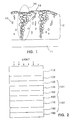
- a thin microcrystalline silicon semiconductor film according to the present invention comprises an amorphous phase with a crystallite aggregate phase composed of crystallites aggregated in a prismatic or conical form.
- a thin microcrystalline silicon semiconductor film according to the present invention comprises an amorphous phase with crystallites contained therein. A portion of the crystallites is dispersed as individual crystallites and the remaining portion of the crystallites is in the form of a prismatic or conical crystallite aggregate phase.
- a photovoltaic device comprises a thin p-type semiconductor film, a thin substantially intrinsic semiconductor film and a thin n-type semiconductor film stacked one over another.
- the thin substantially intrinsic semiconductor film is the above-described thin microcrystalline silicon semiconductor film of the present invention.
- a stacked-structure tandem photovoltaic device comprises a first stacked p-i-n semiconductor structure and a second stacked p-i-n semiconductor structure stacked tdgether in series.
- the first stacked p-i-n semiconductor structure is composed of a first thin p-type semiconductor film, a first thin substantially intrinsic semiconductor film and a first thin n-type semiconductor film
- the second stacked p-i-n semiconductor structure is composed of a second thin p-type semiconductor film, a second thin substantially intrinsic semiconductor film and a second thin n-type semiconductor film.
- the first thin substantially intrinsic semiconductor film is a thin amorphous microcrystalline silicon semiconductor film.
- the second thin substantially intrinsic semiconductor film is the above-described thin microcrystalline silicon semiconductor film of the present invention.
- the first stacked p-i-n semiconductor structure is arranged on a light-impinging side.
- a process according to the present invention is to form a thin microcrystalline silicon semiconductor film on a substrate by RF plasma CVD while using as a raw material at least a compound having silicon in the molecule thereof.
- the process comprises forming first an initial film of the thin microcrystalline silicon semiconductor film to a thickness in a range of from 2 nm to 100 nm on the substrate and then forming a principal film of the thin microcrystalline silicon semiconductor film.
- the deposition rate of the initial film is in a range of from 0.01 nm/sec to 0.1 nm/sec and the deposition rate of the principal film is greater than the deposition rate of the initial film and is in a range of from 0.1 nm/sec to 2 nm/sec.
- microcrystalline silicon contains many defects when formed into a film, and has a band gap approximately as wide as crystalline silicon.
- Conventional solar cells making use of one or more microcrystalline silicon layers are therefore extremely small or low in fill factor and open-circuit voltage compared with those making use of amorphous silicon, resulting in the provision of only those having a low photovoltaic efficiency.
- RF plasma CVD for example, is employed upon deposition of such a microcrystalline silicon layer, deposition of a material having such a high crystalline fraction as reaching close to 100% into a film requires a high hydrogen dilution. The deposition rate is therefore lowered to 0.01 to 0.05 nm/sec, resulting in a serious disadvantage in productivity.
- the present inventors have hence proceeded with an extensive investigation. As a result, it has been found that characteristics of a solar cell making use of microcrystalline silicon semiconductor as an intrinsic layer, especially its open-circuit voltage and photo-deterioration characteristics are dependent heavily on the distribution and structure of crystallites in a thin microcrystalline silicon semiconductor film as the substantially intrinsic semiconductor layer. It has also been found that as a condition for the formation of the microcrystalline silicon film, it can be formed at a deposition rate of 0.1 nm/sec or higher, leading to the finding that an improvement can be expected in productivity over the conventional technique making use of RF plasma CVD.
- a solar cell having an increased open-circuit voltage requires to form a prismatic or conical phase by aggregation of crystallites, each being of 2 to 1000 nm, more preferably 5 to 80 nm in size, and also to include an amorphous silicon phase in a proportion of at least 20% or so.
- the crystalline fraction should preferably be in a range of from 5 to 80%.
- crystallite as used herein means silicon single crystal grains which are observed in an amorphous phase and can be readily confirmed on a transmission electron micrograph or the like.
- the thin microcrystalline silicon semiconductor film according to the present invention is characterized in that it comprises an amorphous phase with a crystallite aggregate phase composed of crystallites aggregated in a prismatic or conical form. This is a novel structure which has been found for the first time by the present inventors. A description will hereinafter be made of the thin microcrystalline silicon semiconductor film according to the present invention.
- the thin microcrystalline silicon semiconductor film according to the present invention is in the form of a thin amorphous silicon semiconductor film (an amorphous phase) 12 containing crystallites 13.
- the crystallites 13 are contained as crystalline aggregate phases 14 which have been formed by their aggregation into prismatic or conical forms.
- This thin microcrystalline silicon semiconductor film is formed on a substrate 11.
- the prismatic or conical crystallite aggregate phases 14 are not absolutely required to have a complete prismatic or conical shape and may take a shape formed by compounding, combining or otherwise mixing a prism and a cone together.
- the thin microcrystalline silicon semiconductor film according to the present invention may contain additional crystallites 13 dispersed as mutually-independent, individual crystallites in the amorphous phase 12.
- FIG. 1 also shows the crystallites 13 independently dispersed in the amorphous phase 12. The structures of the amorphous phase 12, crystallites 13 and crystallite aggregate phases 14 as shown in FIG. 1 can be readily confirmed by observation of a transmission electron micrograph or the like.
- the crystalline fraction is 80% at most, with 5 to 80% being preferred.
- the thin microcrystalline silicon semiconductor film according to the present invention is clearly distinguished from conventionally known microcrystalline films.
- the crystallization degree is as high as 90 to 100%. This value is far greater than crystallization degrees of thin microcrystalline silicon films according to the present invention.
- the size of each crystallite is preferably from 2 to 1,000 nm, more preferably from 5 to 80 nm.
- the thin microcrystalline silicon film according to the present invention especially the prismatic or conical crystallite aggregate phases in the thin microcrystalline silicon film are formed, for example, by plasma CVD, photo-assisted CVD or heat-assisted CVD while using a compound, which contains a silicon atom in its molecule, as a feed gas. It is particularly preferred to conduct continuous formation of films by RF plasma CVD. For this continuous formation, it is preferred to use the feed gas in the form of a mixed gas diluted with hydrogen. When such a mixed gas is employed, the mixed gas should preferably be proportioned to contain the silicon-containing compound in an amount of at least 0.01% by volume.
- a film portion to be formed initially on the substrate that is, a film portion to a thickness of from 2 to 100 nm from the substrate at a low speed, namely, at a deposition rate of from 0.01 to 0.1 nm/sec, followed by the growth of the remaining film portion at a higher deposition rate of 0.1 to 2 nm/sec.
- the film formed first on the substrate at the relatively low deposition rate is called the "initially-formed film”
- the film formed at the relatively high deposition rate subsequent to the formation of the initially-formed film is called the "principal film”.
- the "initially-formed film” is also called the "initial film”.
- crystallites growing on these origin nuclei tend to have a greater size than the crystallites as the origin nuclei and aggregation of such large crystallites can provide the resulting crystallite aggregate phases with properties similar to those of crystalline phases. If a crystallite aggregate phase becomes conical by the provision of an origin nucleus by an initially-formed film, the apex of the cone is usually located on a side of the initially-formed film.
- a mixed gas which includes a compound containing silicon in its molecule and, if necessary, hydrogen is prepared preferably in such a way that the concentration by volume of the compound containing silicon falls in a range of from 0.01 to 100%.
- RF plasma CVD making use of the mixed gas as a feed gas, a film portion of a thickness of about 2 to 100 nm form a substrate is formed as an initially-formed film at a deposition rate of from 0.01 to 0.1 nm/sec. Over this initially-formed film, a principal film is then formed at a deposition rate of from 0.1 to 2 nm/sec.
- this thin microcrystalline silicon semiconductor film When used as a photovoltaic device, it is effective to form the initially-formed film by a film, which contains crystallites of a size in a range of from 20 to 50 nm and has a dark conductivity of from 1 x 10 -11 to 1 x 10 -7 S/cm, so that the open-circuit voltage can be increased.
- the present inventors have found that use of the above-described thin microcrystalline silicon semiconductor film makes it possible to provide a semiconductor device having excellent characteristics, more specifically, a photovoltaic device having an open-circuit voltage close to that available from one making use of amorphous silicon without substantial reductions in short-circuit current and fill factor, equipped with improved light stability and requiring a substantially-shortened film-forming time.
- This photovoltaic device has the construction that on a substrate, a first electrode, a thin semiconductor film of a first conductivity type, a thin substantially intrinsic semiconductor film, a thin semiconductor film of a second conductivity type opposite to the above-described first conductivity type, and a second electrode are stacked one over the other.
- the thin substantially intrinsic semiconductor film is formed of the above-described thin microcrystalline silicon semiconductor film.
- the proportion of crystallites contained in an amorphous phase is in the range of from 5 to 80% and the crystallites have a size in the range of from 2 to 1,000 nm, more preferably from 5 to 80 nm.
- the thin microcrystalline silicon semiconductor film contains prismatic or conical phases formed by aggregation of such crystallites.
- the photovoltaic device is one having the construction that described specifically, a glass sheet with a tin oxide layer formed as a first electrode thereon is used as a substrate, a p-type semiconductor layer, an i-type semiconductor layer consisting of the above-described thin microcrystalline silicon semiconductor film, and an n-type semiconductor layer are successively formed and stacked on the substrate, and silver is used as a second electrode.
- a translucent electrode is used as the second electrode if a non-translucent substrate or electrode is used as the substrate or the first electrode.
- the term "thin substantially intrinsic microcrystalline silicon semiconductor film” means that forming a photoactive region in a silicon solar cell.
- this thin intrinsic microcrystalline silicon semiconductor film can be readily formed from a compound containing silicon in its molecule or a like substance by applying plasma CVD, photo-assisted CVD or heat-assisted CVD. Use of plasma CVD is particularly preferred.
- a plasma can be produced by applying a d.c. or a.c. voltage across plasma-generating electrodes.
- the frequency of an alternating current usable for the generation of a plasma may range from 20 Hz to 100 MHz. Especially, 50 Hz and 60 Hz, the commercial power frequencies, and 13.56 MHz, the radio frequency (RF) allocated for ISM (Industrial, Scientific and Medical use), are frequencies preferred for use.
- a compound containing one or more silicon atoms in its molecule is used as a feed gas.
- feed gases include silane compounds represented by the formula Si n H n+2 (n: a positive integer of 1 or greater), and halogenated silane compounds represented by the formula SiH n X 4-n (X: a halogen, i.e., fluorine or chlorine, n: a positive integer of from 1 to 4) or Si 2 H n X 6-n (X: a halogen, i.e., fluorine or chlorine, n: a positive integer of from 1 to 6).
- feed gases which can be easily used in industry are monosilane (SiH 4 ), disilane (Si 2 H 6 ), trisilane (Si 3 H 8 ), tetrafluorosilicon (SiF 4 ), difluorosilane (SiH 2 F 2 ), trifluorosilane (SiHF 3 ), monofluorosilane (SiH 3 F), and hexafluorodisilane (Si 2 F 6 ).
- an initial film is first formed to a small thickness at a relatively low deposition rate, followed by the formation of a thin microcrystalline film as a principal film at a relatively high deposition rate.
- the formation of the initial film is carried out by controlling plasma-generating power within a range of from 0.01 mW/cm 2 to 100 W/cm 2 in terms of power density, diluting the feed gas with hydrogen to make the concentration of the feed gas fall within a range of from 0.01 to 100% by volume and then using the mixed gas so diluted.
- the concentration of the feed gas ranges preferably from 0.1 to 10%, more preferably from 0.1 to 2%.
- This feed gas may be diluted further with an inert gas such as argon or helium.
- the substrate temperature is from 50 to 500°C, preferably from 50 to 350°C, notably from 75 to 250°C, while the deposition pressure is from 0.01 to 10 Torr, preferably from 0.03 to 5 Torr, most preferably from 0.035 to 2.0 Torr.
- Introduction of the feed gas is conducted through a gas flowmeter. Its flow rate ranges, for example, from 1 cc/min to 1,000 cc/min as measured under standard conditions (0°C, 1 atm). It is preferred to control the deposition rate of the initial film within a range of from 0.01 to 0.1 nm/sec under these deposition conditions. Further, the thickness of the initial film is from 2 to 100 nm, with 2 to 10 nm being preferred.
- the plasma-generating power is controlled within a range of from 0.01 mW/cm 2 to 100 W/cm 2 in terms of power density, and a mixed gas obtained by diluting the above-described feed gas with hydrogen to make the concentration of the feed gas fall within a range of from 0.01 to 100% by volume is used as a raw material.
- the concentration of the feed gas ranges preferably from 0.1 to 20%, more preferably from 0.1 to 5%.
- This feed gas may be diluted further with an inert gas such as argon or helium.
- the substrate temperature is from 50 to 500°C, preferably from 50 to 350°C, notably from 75 to 250°C, while the deposition pressure is from 0.01 to 10 Torr, preferably from 0.03 to 5 Torr, most preferably from 0.035 to 2.0 Torr.
- Introduction of the feed gas is conducted through a gas flowmeter. Its flow rate ranges, for example, from 1 cc/min to 1,000 cc/min as measured under standard conditions. It is preferred to control the deposition rate of the microcrystalline silicon film within a range of from 0.1 to 2 nm/sec, preferably from 0.1 to 1 nm/sec under these deposition conditions.
- the thickness of the thin substantially intrinsic semiconductor film formed as described above ranges from 200 nm to 10 ⁇ m, including the initial film.
- the crystallite size and crystalline fraction of the thin microcrystalline silicon semiconductor film can be determined by Raman scattering spectroscopy, X-ray diffraction, transmission electron microscopy or the like. As simple and convenient methods, the crystalline fraction can be calculated from the intensity of Raman scattering or X-ray diffraction, whereas the crystallite size can be calculated from the peak width at half height in an X-ray diffraction spectrum. For the size determination of extremely small crystallites, a measurement relying upon a transmission electron micrograph is useful.
- the crystalline fraction measured using the transmission electron micrograph is defined as an area ratio of crystalline regions to amorphous regions in the micrograph, and the crystallite size is defined as the greatest one of diagonals or diameters in individual regions of a polygonal or elongated circular shape observed as crystallites. Measurements by such a transmission electron micrograph are very useful for the determination of the distribution and structure of crystallites.
- the thin p-type semiconductor film employed in the photovoltaic device include a thin film of p-type amorphous silicon, amorphous silicon carbide, microcrystalline silicon, microcrystalline silicon carbide or carbon-containing microcrystalline silicon, a multilayer film of amorphous silicon carbides having different carbon contents, and a multilayer film of amorphous silicon and amorphous carbon.
- a thin film of p-type microcrystalline' silicon, microcrystalline silicon carbide or carbon-containing microcrystalline silicon is more preferred.
- a process for the formation of the p-type semiconductor layer plasma CVD or photo-assisted CVD is used.
- silane, disilane or trisilane is employed as a silicon compound.
- diborane, trimethylboron, trifluoroboron or the like is preferred.
- a carbon-containing compound a saturated hydrocarbon such as methane or ethane, an unsaturated hydrocarbon such as ethylene or acetylene, or an alkylsilane such as monomethylsilane or dimethylsilane is used.
- Such a mixed gas may be diluted with an inert gas such as helium or argon or with hydrogen as needed without departing from the scope of the present invention.
- an inert gas such as helium or argon
- hydrogen as needed without departing from the scope of the present invention.
- the film thickness ranges from 2 to 50 nm, with 5 to 20 nm being particularly preferred, the depositing temperature ranges from 50 to 400°C, preferably from 50 to 250°C, and the forming pressure ranges from 0.01 to 5 Torr, preferably from 0.03 to 1.5 Torr, notably from 0.035 to 1.0 Torr.
- the RF power should be controlled within a range of from 0.01 mW/cm 2 to 10 W/cm 2 .
- a thin n-type microcrystalline film or a thin n-type amorphous film can be used effectively.
- Effectively usable examples of such thin films include a thin n-type microcrystalline silicon film, a thin carbon-containing microcrystalline silicon film, a thin microcrystalline silicon carbide film, a thin amorphous silicon film, a thin amorphous silicon carbide film, and a thin amorphous silicon germanium film.
- These thin n-type semiconductor films can be easily formed by mixing a compound containing a Group V element of the Periodic Table, such as phosphine or arsine, and hydrogen with a raw material chosen as needed depending on the target thin semiconductor film from compounds containing silicon in their molecules, compounds containing germanium in their molecules, such as germane and silylgermane, hydrocarbon gases and the like, and applying plasma CVD or photo-assisted CVD. Further, dilution of the feed gas with an inert gas such as helium or argon by no means impairs the effects of the present invention. To the contrary, upon formation of a thin microcrystalline silicon film, it is more preferred to dilute the mixed gas with a large volume of hydrogen.
- a compound containing a Group V element of the Periodic Table such as phosphine or arsine
- hydrogen a raw material chosen as needed depending on the target thin semiconductor film from compounds containing silicon in their molecules, compounds containing germanium in their molecules, such as germane and silylgerman
- the depositing temperature ranges from 50 to 400°C, preferably from 100 to 350°C, and the forming pressure ranges from 0.01 to 5 Torr, preferably from 0.03 to 1.5 Torr.
- the RF power should be controlled within a range of from 0.01 to 10 W/cm 2 .
- the n-type semiconductor layer is formed with a thin microcrystalline silicon film, it is preferred to control the RF power within a range of from 0.1 to 10 W/cm 2 .
- a thickness of from 10 to 50 nm is sufficient for the thin n-type semiconductor film.
- silicon hydrides such as monosilane, disilane and trisilane
- alkyl-substituted silicon hydrides such as monomethylsilane, dimethylsilane, trimethylsilane, tetramethylsilane, ethylsilane and diethylsilane
- silicon hydrides containing one or more radically-polymerizable, unsaturated hydrocarbon groups such as vinylsilane, divinylsilane, trivinylsilane, vinyl-disilane, divinyldisilane, propenylsilane and ethenylsilane
- fluorinated silicons obtained by either partly or wholly substituting the hydrogen atoms of these silicon hydrides with fluorine atoms.
- hydrocarbon gas examples include methane, ethane, propane, ethylene, propylene and acetylene. These hydrocarbon gases can be conveniently used when it is desired to modify the optical band gap in the formation of a thin carbon-containing microcrystalline silicon film, a thin microcrystalline silicon carbide film or the like.
- materials such as alkyl-substituted silicon hydrides, silicon hydrides containing one or more radically-polymerizable, unsaturated hydrocarbon groups in their molecules and fluorinated silicons obtained by either partly or wholly substituting the hydrogen atoms of these silicon hydrides with fluorine atoms are also useful.
- the substrate of the photovoltaic device has a thickness and surface configurations sufficient to allow a solar cell, which is to be formed thereon, to retain its shape and is made of a material withstandable temperatures to which the substrate may be exposed during the formation of the solar cell.
- the substrate include glass sheets such as borosilicate glass, soda-lime glass and quartz glass sheets; ceramic sheets such as alumina, boron nitride and silicon sheets; metal sheets such as aluminum, stainless steel, chromium, titanium and molybdenum sheets, and ceramic sheets coated with these metals; polymer sheets or films such as polyethersulfon (PES), polyetheretherketone (PEEK), polycarbonate (PC), polyethylene terephthalate (PET), polyethylene naphthalate (PEN), polyamide, and polyimide plates and sheets; and polymer sheets or films coated with the above-described metals.
- glass sheets such as borosilicate glass, soda-lime glass and quartz glass sheets
- ceramic sheets such as alumina, boron nitride and silicon sheets
- metal sheets such as aluminum, stainless steel, chromium, titanium and molybdenum sheets, and ceramic sheets coated with these metals
- polymer sheets or films such as polyethersulfon (PES), polyether
- electrode means a translucent electrode or a metal electrode.
- a translucent material such as tin oxide, indium oxide and zinc oxide; and translucent metals and the like.
- metal electrode it is possible to use a metal which is chosen as desired from aluminum, chromium, nickel-chromium alloys, silver, gold, platinum and the like.
- the semiconductors and materials at least which are indispensable for the construction of the photovoltaic device (solar cell), have been described above.
- the introduction of the interfacial layer, which acts to improve the performance of the solar cell, at the interface between the p-type semiconductor layer and the i-type semiconductor layer, between the i-type semiconductor layer and the n-type semiconductor layer or between the first electrode and the first p-type semiconductor layer is not essential for the practice of the present invention.
- an interfacial layer can be used as desired depending on the purpose without impairing the objects of the present invention.
- an interfacial layer can be introduced at the interface between the first n-type semiconductor layer and the second p-type semiconductor layer in addition to the above-described individual interfaces.
- a p/i interfacial layer formed of a thin amorphous silicon carbide film between the thin p-type doped semiconductor film and the thin substantially intrinsic silicon semiconductor film in the above-described p-i-n solar cell which makes use of the thin microcrystalline silicon semiconductor film as an intrinsic semiconductor layer.
- the thin amorphous silicon carbide film which is formed as the interfacial layer between the thin p-type doped semiconductor film and the thin substantially intrinsic silicon semiconductor film, can be readily formed from a compound containing one or more silicon atoms in its molecule or a like substance by applying plasma CVD, photo-assisted CVD or heat-assisted CVD. Use of plasma CVD or mercury-sensitized CVD is particularly preferred.
- a plasma can be produced by applying a d.c. or a.c. voltage across plasma-generating electrodes.
- the frequency of an alternating current usable for the generation of a plasma may range from 20 Hz to 100 MHz. Especially, 50 Hz and 60 Hz, the commercial power frequencies, and 13.56 MHz, the ISM frequency are frequencies preferred for use. It is however to be noted that the frequency of this plasma-producing current including the direct current does not give any problem to the practice of the present invention.
- the power for producing a plasma for the formation of the p/i interfacial layer is in a range of from 0.001 mW/cm 2 to 100 W/cm 2 , preferably from 0.01 mW/cm 2 to 10 mW/cm 2 as expressed in terms of power density.
- Illustrative of the raw material employed upon formation of the thin amorphous silicon carbide film include silane, disilane and trisilane as silicon compounds.
- usable examples of carbon-containing compounds include saturated hydrocarbons such as methane and ethane; unsaturated hydrocarbons such as ethylene and acetylene; and alkylsilanes such as monomethylsilane and dimethylsilane. Dilution of a mixed gas of such raw materials with an inert gas such as helium or argon or with hydrogen as needed does not prevent at all the practice of the present invention. It is also a preferred embodiment to mix diborane, trimethylboron, trifluoroboron or the like for the provision of p-type conductivity.
- the preferred concentration of boron in an amorphous silicon carbide film formed by mixing such a boron-containing compound ranges from 10 15 to 10 18 cm -3 .
- the film thickness ranges from 2 to 50 nm, with 5 to 20 nm being particularly preferred, the depositing temperature ranges from 50 to 400°C, preferably from 50 to 250°C, most preferably from 75 to 250°C, and the forming pressure ranges from 0.01 to 5 Torr, preferably from 0.03 to 1.5 Torr, notably from 0.035 to 1.0 Torr.
- the photovoltaic device of the stacked tandem structure can also be fabricated.
- the thin microcrystalline silicon semiconductor film according to the present invention has a band gap effectively narrower than an amorphous silicon film, it is effective and preferred for an improved light absorption rate to use amorphous silicon for the substantially intrinsic semiconductor layer in the element on the light-impinging side and to apply the thin microcrystalline silicon film according to the present invention for the substantially intrinsic semiconductor layer in the element on the light-non-impinging side upon stacking the two p-i-n photovoltaic elements together.
- a photovoltaic device of the stacked tandem structure obtained by stacking a stacked p-i-n semiconductor structure A - in which a thin amorphous silicon semiconductor film is contained as a thin substantially intrinsic semiconductor film layer - with a stacked p-i-n semiconductor structure B - in which the above-mentioned thin microcrystalline silicon semiconductor film is contained as a thin substantially intrinsic semiconductor film layer - in series to have a construction of AB
- the stacked p-i-n semiconductor structure A is arranged to assume a position on the light-impinging side.
- the use of the thin microcrystalline silicon semiconductor film as the thin n-type doped semiconductor film which exists between the two thin substantially intrinsic semiconductor film layers in the above photovoltaic device of the stacked tandem structure is effective and preferred for the provision of an improved fill factor.
- photovoltaic devices of such a stacked tandem structure it is most common to have the structure that, as shown in FIG.
- a glass sheet equipped with a translucent conductive film thereon such as tin oxide, zinc oxide or the like is used as a substrate; a p-type semiconductor layer, an i-type amorphous silicon semiconductor layer, an n-type microcrystalline silicon semiconductor layer, another p-type semiconductor layer, an i-type microcrystalline silicon semiconductor layer and an n-type semiconductor layer are formed and stacked on the substrate in the order that they have been presented; and silver is used as a second electrode.
- the photovoltaic device of the stacked tandem structure shown in FIG. 2 has the structure that on a glass sheet 110 as a substrate, a translucent conductive film 120, a p-type semiconductor layer 130, an i-type amorphous silicon semiconductor layer 140, an n-type microcrystalline silicon semiconductor layer 150, a p-type semiconductor layer 160, an i-type microcrystalline silicon semiconductor layer 170, an n-type semiconductor layer 180 and a silver electrode 190 are successively stacked one over the other.
- this tandem photovoltaic device has been obtained by monolithically stacking two layers of p-i-n photovoltaic elements 101,102 one over the other.
- the first p-i-n photovoltaic element 101 is constructed of the p-type semiconductor layer 130, the i-type amorphous silicon semiconductor layer 140 and the n-type microcrystalline silicon semiconductor layer 150
- the second p-i-n photovoltaic element 102 is constructed of the p-type semiconductor layer 160, the i-type microcrystalline silicon semiconductor layer 170 and the n-type semiconductor layer 180. Light impinges the photovoltaic elements 101,102 from the side of the glass substrate 110.
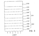
- an photovoltaic device of the stacked tandem structure is formed into such a construction that, as is illustrated in FIG. 3, a translucent electrode having translucency is used as a second electrode and a thin amorphous silicon semiconductor film is arranged as a substantially intrinsic semiconductor layer on a light-impinging side.
- This tandem photovoltaic device has been obtained by monolithically stacking two layers of p-i-n photovoltaic elements 201,202 one over the other.
- the first p-i-n photovoltaic element 201 is constructed of the n-type semiconductor layer 240, the i-type microcrystalline silicon semiconductor layer 250 and the p-type silicon semiconductor layer 260, while the second p-i-n photovoltaic element 202 is constructed of the n-type microcrystalline silicon semiconductor layer 270, the i-type amorphous silicon semiconductor layer 280 and the p-type semiconductor layer 290.
- a thin carbon-containing microcrystalline silicon film, a thin microcrystalline silicon carbide film or the like may be used instead of the thin n-type microcrystalline silicon semiconductor film as a thin film having crystallinity, that is, as the n-type semiconductor layer employed between the two thin substantially intrinsic semiconductor layers.
- Effectively usable examples of the thin n-type amorphous silicon semiconductor film include a thin amorphous silicon film, a thin amorphous silicon carbide film, and a thin amorphous silicon germanium film.
- These thin n-type semiconductor films can be easily formed by mixing a compound containing a Group V element of the Periodic Table, such as phosphine or arsine, and hydrogen with a raw material chosen as needed depending on the target thin semiconductor film from compounds containing silicon in their molecules, compounds containing germanium in their molecules, such as germane and silylgermane, hydrocarbon gases and the like, and applying plasma CVD or photo-assisted CVD. Further, dilution of the feed gas with an inert gas such as helium or argon by no means impairs the effects of the present invention. To the contrary, upon formation of a thin microcrystalline silicon film, it is more preferred to dilute the mixed gas with a large volume of hydrogen.
- a compound containing a Group V element of the Periodic Table such as phosphine or arsine
- hydrogen a raw material chosen as needed depending on the target thin semiconductor film from compounds containing silicon in their molecules, compounds containing germanium in their molecules, such as germane and silylgerman
- the depositing temperature ranges from 50 to 400°C, preferably from 100 to 350°C, and the forming pressure ranges from 0.01 to 5 Torr, preferably from 0.03 to 1.5 Torr.
- the RF power should be controlled within a range of from 0.1 to 10 W/cm 2 .
- a thickness of from 10 to 50 nm is sufficient for the thin n-type semiconductor film. Existence or non-existence of crystallinity in the film so formed can be easily confirmed by an X-ray diffraction spectrum, a Raman scattering spectrum, a transmission electron micrograph or the like.
- the thin p-type semiconductor film, the thin n-type semiconductor film positioned on the outer side of the two thin substantially intrinsic semiconductor films, the thin substantially intrinsic microcrystalline silicon semiconductor film, the electrodes and the substrate can be formed similarly as in the above-described p-i-n photovoltaic device.
- the film located on the light-impinging side forms one of the photoactive regions of the silicon solar cell and as mentioned above, is made of amorphous silicon.
- amorphous silicon In addition to amorphous silicon, one or more hetero-elements effective for controlling the band gap of the thin film, led by hydrogen and fluorine and including germanium, tin, carbon, nitrogen, oxygen and the like can also be contained.
- the thin substantially intrinsic semiconductor film located on the light-impinging side can be readily formed from a compound containing silicon in its molecule or a like substance by applying plasma CVD, photo-assisted CVD or heat-assisted CVD.
- production of the plasma can be effected by applying a d.c. or a.c. voltage across plasma-generating electrodes.
- the frequency of an alternating current may range from 20 Hz to 100 MHz. Especially, 50 Hz and 60 Hz, the commercial power frequencies, and 13.56 MHz, the ISM frequency, are frequencies preferred for use. However, the frequency of this plasma-producing current including the direct current should not be limited to those mentioned above.
- the plasma-producing power should be in a range of from 0.001 mW/cm 2 to 100 W/cm 2 in terms of power density.
- a description will hereinafter be made of formation of the thin substantially intrinsic semiconductor film located on the light-impinging side by plasma CVD.
- Examples of the feed gas include silane compounds represented by the formula Si n H n+2 (n: a positive integer of 1 or greater), and halogenated silane compounds represented by the formula SiH n X 4-n (X: a halogen, i.e., fluorine or chlorine, n: a positive integer of from 1 to 4) or Si 2 H n X 6-n (X: a halogen, i.e., fluorine or chlorine, n: a positive integer of from 1 to 6).
- Illustrative specific feed gases which can be easily used in industry are monosilane (SiH 4 ), disilane (Si 2 H 6 ), trisilane (Si 3 H 8 ), tetrafluorosilicon (SiF 4 ), difluorosilane (SiH 2 F 2 ), trifluorosilane (SiHF 3 ), monofluorosilane (SiH 3 F), and hexafluorosilane (Si 2 F 6 ).
- Such a feed gas may be diluted with an inert gas, such as argon or helium, or with hydrogen gas. When diluted, the concentration of the feed gas ranges from 1 to 100% by volume.
- a gas containing a hetero-element for the control of the band gap monogermane, germanium tetrachloride, stannane (SnH 4 ), tin tetrachloride, tin fluoride, a saturated hydrocarbon compound such as methane or ethane, an unsaturated hydrocarbon compound such as ethylene or acetylene, an organosilane compound such as methylsilane, dimethylsilane, disilylsilane or dimethyldisilane, nitrogen, nitrous oxide (N 2 O), oxygen, carbon dioxide, steam or the like.
- monogermane germanium tetrachloride, stannane (SnH 4 ), tin tetrachloride, tin fluoride, a saturated hydrocarbon compound such as methane or ethane, an unsaturated hydrocarbon compound such as ethylene or acetylene, an organosilane compound such as methylsilane, dimethylsi
- the concentration of a diluted feed gas ranges from 1 to 100% by volume.
- the effects of the present invention will not be impaired at all even by combined use of a conventional technique known in the field of formation of thin intrinsic semiconductor films, for example, even when extremely trace amounts of diborane and phosphine are intentionally mixed at the same time with a feed gas to add boron atoms and phosphorus atoms in trace amounts to the resulting thin substantially intrinsic semiconductor film.
- feed gas is conducted through a gas flowmeter. Its flow rate ranges from 1 cc/min to 1,000 cc/min (as measured under standard conditions). Further, the depositing temperature ranges from 50 to 400°C, preferably, from 50 to 350°C, while the forming pressure ranges from 0.01 to 100 Torr, preferably, from 0.03 to 1.5 Torr.
- photo-assisted CVD or heat-assisted CVD can also be used for the formation of the thin substantially intrinsic semiconductor film which is located on the light-impinging side and is composed of amorphous silicon. No particular limitation is imposed on the film-forming process upon practicing the present invention.
- This thin substantially intrinsic semiconductor layer may be formed of a first layer, which is relatively thin and functions as a buffer layer, and a second layer which is formed over the first layer and is relatively thick.
- the thickness of the first layer ranges from 10 to 200 nm while that of the second layer ranges from 50 nm to 5 ⁇ m.
- Microcrystalline silicon films according to the present invention are also useful for the performance heightening of silicon semiconductor devices such as TFTs (Thin Film Transistors) and image sensors.
- TFTs Thin Film Transistors
- image sensors image sensors
- crystalline silicon can be formed at a low substrate temperature, especially, in TFTs, microcrystalline silicon films according to the present invention are very useful in providing active matrix liquid crystal displays, in which TFTs are used, with a higher aperture rate.
- That film deposition system was constructed of five chambers which consisted of two doped-film depositing chambers for forming a thin p-type and n-type semiconductor films, respectively, an i-type layer depositing chamber for forming a thin substantially intrinsic semiconductor layer, a sample loading chamber, and a sample unloading chamber.
- the loading chamber was evacuated to a reduced pressure of 1 x 10 -6 Torr and the substrate was heated at 160°C for 30 minutes.
- the substrate was then transferred to the p-type doped film depositing chamber, where a thin p-type microcrystalline silicon film was deposited.
- the deposition of the thin p-type microcrystalline silicon film was conducted by charging, as a feed gas, monosilane, diborane and hydrogen at a ratio of 1/0.003/100 and practicing RF plasma CVD at a pressure of 0.2 Torr, a substrate temperature of 160°C and an RF power of 0.64 W/cm 2 .
- the frequency employed for producing an RF discharge was set at 13.56 MHz.
- the deposition rate of the thin p-type microcrystalline silicon film was 0.08 nm/sec and the deposition time was set at 250 sec, so that the thin p-type microcrystalline silicon film was formed to a thickness of 20 nm.
- the substrate was next transferred to the i-type layer depositing chamber, where a thin microcrystalline silicon film was deposited as an initially-formed film (initial film) of a substantially intrinsic semiconductor film to a thickness of 10 nm by charging monosilane and hydrogen at a ratio of 2/98 and practicing RF plasma CVD at a pressure of 0.15 Torr, a substrate temperature of 200°C and an RF power of 0.64 W/cm 2 .
- a principal film of the thin microcrystalline silicon film was then formed to a thickness of 1,000 nm by charging monosilane and hydrogen at a ratio of 3/97 and practicing RF plasma CVD at a pressure of 0.15 Torr, a substrate temperature of 200°C and an RF power of 0.64 W/cm 2 , whereby the substantially intrinsic semiconductor film was completed.
- the substrate was transferred to the n-type doped layer depositing chamber. That doped layer depositing chamber was charged with a feed gas, namely, monosilane, phosphine and hydrogen at such flow rates as giving a ratio of 0.5/0.06/120.
- a thin n-type semiconductor film was formed to a thickness of 40 nm by practicing RF plasma CVD at a pressure of 0.2 Torr, a substrate temperature of 160°C and a frequency of 13.56 MHz. At that time, the RF power was 0.8 W/cm 2 .
- the substrate was thereafter taken out of the film-depositing system, and a translucent conductive film of indium oxide and tin oxide (ITO) and a silver electrode were successively formed by vacuum evaporation.
- ITO indium oxide and tin oxide
- Photovoltaic characteristics of the p-i-n silicon solar cell fabricated as described above were measured by irradiating artificial sunlight having an AM (Air Mass) value of 1.5 and an energy density of 100 mW/cm 2 from a solar simulator.
- Its fill factor FF, short-circuit current I sc and photovoltaic efficiency ⁇ were 0.55, 14.6 mA/cm 2 and 5.0%, respectively. The solar cell therefore showed outstanding initial characteristics.
- the solar cell was irradiated at a temperature of 40°C over 800 hours by light having an energy density of 100 mW/cm 2 under a halogen lamp. Its photovoltaic characteristics were then measured. As a result, the solar cell was found to have an open-circuit voltage V oc of 0.61 V, a fill factor FF of 0.54, a short-circuit current I sc of 14.0 mA/cm 2 , a photovoltaic efficiency ⁇ of 4.6%. Its deterioration rate of photovoltaic efficiency was determined to be 8%. The solar cell was therefore found to have excellent resistance to deterioration.
- the i-type layer was formed of two phases, one being a phase formed of crystallite aggregates grown into prismatic or conical shapes and the other being a phase with individual crystallites dispersed in an amorphous matrix.
- the accuracy of the deposition rate is also considered to be ⁇ 5%.
- the dark conductivity of the thin film was 1 x 10 -7 S/cm. Based on a transmission electron micrograph of that sample, the size of the greatest crystallite was determined to be 5 nm.
- microcrystalline silicon film (principal film) formed subsequent to the formation of the initial film.
- the deposition rate, crystallite size and crystalline fraction were 0.14 nm/sec, 5 to 27 nm and 70%, respectively.
- Example 1 a solar cell was fabricated as in Example 1 except that the conditions for the formation of the initial film of the thin microcrystalline silicon film and those for the subsequent formation of the principal film were changed.
- Table 1 presents forming conditions for each microcrystalline silicon film making up a substantially intrinsic semiconductor layer
- Table 2 shows characteristics of each initial film and its corresponding principal film measured as single films as in Example 1
- Table 3 summarizes characteristics of each solar cell so obtained.
- Example 1 Following the procedures of Example 1, remaining gas was purged under vacuum subsequent to the formation of a thin p-type microcrystalline silicon film.
- An amorphous silicon carbide film was then formed as a p/i interfacial layer to a thickness of 15 nm by charging monosilane, methane and hydrogen at a ratio of 5/5/12.5 and practicing RF plasma CVD at a pressure of 0.1 Torr, a substrate temperature of 160°C and an RF power of 0.06 W/cm 2 .
- the procedures of Example 1 were then followed to form a substantially intrinsic semiconductor layer and a thin n-type semiconductor film, so that a silicon solar cell was completed.
- Photovoltaic characteristics of that solar cell for artificial sunlight having an AM value of 1.5 and an energy density of 100 mW/cm 2 were then measured.
- the solar cell was found to have an open-circuit voltage V oc of 0.86 V and therefore, had been extremely improved in open-circuit voltage over the conventional art.
- Its fill factor FF, short-circuit current I sc and photovoltaic efficiency ⁇ were 0.60, 10.1 mA/cm 2 and 5.2%, respectively.
- the solar cell therefore showed outstanding characteristics.
- the solar cell was irradiated at a temperature of 40°C over 800 hours by light having an energy density of 100 mW/cm 2 under the halogen lamp. Its post-irradiation photovoltaic characteristics were measured.
- the solar cell was found to have an open-circuit voltage V oc of 0.84 V, a fill factor FF of 0.57, a short-circuit current I sc of 10.0 mA/cm 2 , a photovoltaic efficiency ⁇ of 4.8%. Its deterioration rate of photovoltaic efficiency was hence determined to be 8%. Deterioration was therefore successfully reduced.
- Thin films which were equivalent to the p/i interfacial layer in the silicon solar cell, were formed to a thickness of 500 nm on a quartz substrate and a crystalline silicon substrate, respectively. They were subjected to secondary ion mass spectroscopy and light absorption spectroscopy. Those thin films were ascertained to be made of carbon-containing amorphous silicon. They were also found to have a band gap of 2.45 eV.
- a photovoltaic device of the stacked tandem structure was fabricated with two layers of stacked p-i-n semiconductor structures arranged in series.
- the loading chamber was evacuated to a reduced pressure of 1 x 10 -6 Torr.
- the substrate was heated at 160°C for 30 minutes.
- the substrate was then transferred to the p-type doped film depositing chamber, where a thin p-type amorphous silicon carbide film was deposited.
- the formation of the thin p-type amorphous silicon carbide film was conducted by charging, as a feed gas, monosilane, diborane, methane and hydrogen at a ratio of 4/0.06/5/26 and practicing plasma CVD at a pressure of 0.15 Torr, a substrate temperature of 160°C and an RF power of 0.05 W/cm 2 .
- the forming rate of the thin p-type amorphous silicon carbide film was 0.05 nm/sec and the film-forming time was set at 150 sec, so that the thin p-type amorphous silicon carbide film was formed to a thickness of 7.5 nm.
- the formation of the thin p-type amorphous silicon carbide film was then suspended.
- an amorphous silicon carbide film was deposited as a p/i interfacial layer to a thickness of 10 nm by charging monosilane, methane and hydrogen at a ratio of 5/5/12.5 and practicing plasma CVD at a pressure of 0.1 Torr, a substrate temperature of 160°C and an RF power of 0.06 W/cm 2 .
- the substrate was next transferred to an i-type layer depositing chamber, where a thin amorphous silicon film was formed to a thickness of 250 nm by charging monosilane at a flow rate of 10 cc/min (as measured under standard conditions) and practicing RF plasma CVD at a pressure of 0.05 Torr, a substrate temperature of 160°C, a frequency of 13.56 MHz and an RF power of 0.1 W/cm 2 . Subsequent to the formation of the thin i-type semiconductor film, the substrate was transferred to the n-type doped layer forming chamber.
- a thin n-type semiconductor film was formed to a thickness of 10 nm by charging a feed gas, that is, monosilane, phosphine and hydrogen at such flow rates as giving a ratio of 10/0.02/10 and practicing RF plasma CVD at a pressure of 0.10 Torr, a substrate temperature of 160°C, a frequency of 13.56 MHz and an RF power of 0.06 W/cm 2 .
- a feed gas that is, monosilane, phosphine and hydrogen
- a thin p-type microcrystalline silicon film was additionally formed.
- the thin p-type microcrystalline silicon film was formed to a thickness of 20 nm by charging, as a feed gas, monosilane, diborane and hydrogen at a ratio of 1/0.003/100 and practicing PF plasma CVD at a pressure of 0.2 Torr, a substrate temperature of 160°C, a frequency of 13.56 MHz and an RF power of 0.6 W/cm 2 .
- the substrate was next transferred to the i-type layer forming chamber and under the same conditions as those employed upon formation of the substantially intrinsic semiconductor layer in Example 1, a thin microcrystalline film was formed as a second substantially intrinsic semiconductor layer to a thickness of 1,600 nm by RF plasma CVD. At that time, the frequency and RF power were 13.56 MHz and 0.10 W/cm 2 , respectively. Subsequent to the formation of the second thin substantially intrinsic semiconductor layer, the substrate was transferred to the n-type doped layer depositing chamber.
- a second thin n-type semiconductor film was formed to a thickness of 40 nm by charging a feed gas, namely, monosilane, phosphine and hydrogen at such flow rates as giving a ratio of 0.5/0.06/120 and practicing RF plasma CVD at a pressure of 0.2 Torr, a substrate temperature of 160°C, a frequency of 13.56 MHz and an RF power of 0.8 W/cm 2 .
- a feed gas namely, monosilane, phosphine and hydrogen
- Photovoltaic characteristics of that solar cell were measured by irradiating artificial sunlight having an AM value of 1.5 and an energy density of 100 mW/cm 2 from the solar simulator.
- the solar cell was found to have an open-circuit voltage V oc of 1.31 V, a fill factor FF of 0.70 and a short-circuit current I sc of 10.2 mA/cm 2 .
- a high fill factor FF was obtained.
- the photovoltaic efficiency ⁇ was 9.4%, namely, excellent.
- the solar cell was irradiated at a temperature of 40°C over 800 hours by light having an energy density of 100 mW/cm 2 under the halogen lamp.
- the solar cell was found to have an open-circuit voltage V oc of 1.31 V, a fill factor FF of 0.70, a short-circuit current I sc of 9.8 mA/cm 2 , a photovoltaic efficiency ⁇ of 9.0%. Its deterioration rate of photovoltaic efficiency was hence determined to be 4%. Deterioration was therefore successfully reduced.
- a thin n-type semiconductor film was formed to a thickness of 40 nm on a quartz substrate under conditions similar to those employed upon formation of the first thin n-type semiconductor film, that is, by charging a feed gas, namely, monosilane, phosphine and hydrogen at such flow rates as giving a ratio of 10/0.02/10 and practicing RF plasma CVD at a pressure of 0.10 Torr, a substrate temperature of 160°C and an RF power of 0.06 W/cm 2 .
- a Raman scattering spectrum of the thin n-type semiconductor film was then measured. As a result, only a broad peak corresponding to amorphous silicon was observed centering at 480 cm -1 . The film was therefore confirmed to be a thin amorphous silicon film.
- a silicon solar cell was fabricated following the procedures of Example 8 except that only the film-forming conditions for the first thin n-type semiconductor film were changed.
- a first thin n-type semiconductor film was formed to a thickness of 40 nm by charging, as a feed gas, monosilane, phosphine and hydrogen at such flow rates as giving a ratio of 0.5/0.06/120 and practicing RF plasma CVD at a pressure of 0.2 Torr, a substrate temperature of 160°C and an RF power of 0.8 W/cm 2 .
- Photovoltaic characteristics of that solar cell were measured by irradiating artificial sunlight having an AM value of 1.5 and an energy density of 100 mW/cm 2 from the solar simulator.
- the solar cell was found to have an open-circuit voltage V oc of 1.32 V, a fill factor FF of 0.73 and a short-circuit current I sc of 10.4 mA/cm 2 and a photovoltaic efficiency ⁇ of 10.0%.
- the solar cell was irradiated at a temperature of 40°C over 800 hours by light having an energy density of 100 mW/cm 2 under the halogen lamp. Its post-irradiation photovoltaic characteristics were measured.
- the solar cell was found to have an open-circuit voltage V oc of 1.31 V, a fill factor FF of 0.72, a short-circuit current I sc of 9.8 mA/cm 2 , a photovoltaic efficiency ⁇ of 9.2%. Its deterioration rate of photovoltaic efficiency was hence determined to be 8%. Deterioration was therefore successfully reduced.
- a thin n-type semiconductor film was formed to a thickness of 40 nm on a quartz substrate under conditions similar to those employed upon formation of the first thin n-type semiconductor film, that is, by charging a feed gas, namely, monosilane, phosphine and hydrogen at such flow rates as giving a ratio of 0.5/0.06/120 and practicing RF plasma CVD at a pressure of 0.2 Torr, a substrate temperature of 160°C and an RF power of 0.8 W/cm 2 .
- a feed gas namely, monosilane, phosphine and hydrogen
- Example 9 a silicon solar cell was fabricated with an amorphous silicon carbide film formed as a p/i interfacial layer to a thickness of 15 nm in a similar manner to Example 2 between a second thin p-type semiconductor film and a second substantially intrinsic semiconductor layer.
- Photovoltaic characteristics of that solar cell were measured by irradiating artificial sunlight having an AM value of 1.5 and an energy density of 100 mW/cm 2 from the solar simulator.
- the solar cell was found to have an open-circuit voltage V oc of 1.34 V, a fill factor FF of 0.68 and a short-circuit current I sc of 10.2 mA/cm 2 and a photovoltaic efficiency ⁇ of 9.3%.
- the solar cell was irradiated at a temperature of 40°C over 800 hours by light having an energy density of 100 mW/cm 2 under the halogen lamp. Its post-irradiation photovoltaic characteristics were measured.
- the solar cell was found to have an open-circuit voltage V oc of 1.33 V, a fill factor FF of 0.67, and a short-circuit current I sc of 10.1 mA/cm 2 .
- V oc open-circuit voltage
- FF fill factor
- I sc short-circuit current
- Example 1 a silicon solar cell was fabricated as in Example 1 except that the film-forming conditions for the deposition of the initial film of the thin microcrystalline silicon film making up the substantially intrinsic semiconductor layer and those for the subsequent formation of the principal film were changed.
- Table 4 presents forming conditions for each microcrystalline silicon film making up a substantially intrinsic semiconductor layer
- Table 5 shows characteristics of each initial film and its corresponding principal film measured as single films as in Example 1
- Table 6 summarizes characteristics of each solar cell so obtained.
- a thin microcrystalline silicon semiconductor film which features inclusion of prismatic or conical phases formed by aggregation of crystallites having a crystallite size in the range of from 2 to 1,000 nm, as a thin substantially intrinsic semiconductor layer in a p-i-n solar cell leads to improvements in power characteristics owing especially to an improved open-circuit voltage and also to a significant improvement in light stability over those of solar cells making use of materials employed in the conventional art, thereby making it possible to fabricate a solar cell having excellent characteristics.
- the present invention has brought about a significant practical contribution to an improvement in the photovoltaic efficiency of a silicon solar cell.
Applications Claiming Priority (15)
| Application Number | Priority Date | Filing Date | Title |
|---|---|---|---|
| JP37138/95 | 1995-02-24 | ||
| JP3713895 | 1995-02-24 | ||
| JP3713895 | 1995-02-24 | ||
| JP20795795 | 1995-08-15 | ||
| JP20795795 | 1995-08-15 | ||
| JP207957/95 | 1995-08-15 | ||
| JP21608895 | 1995-08-24 | ||
| JP216088/95 | 1995-08-24 | ||
| JP21608895 | 1995-08-24 | ||
| JP26880795 | 1995-10-17 | ||
| JP268807/95 | 1995-10-17 | ||
| JP26880795 | 1995-10-17 | ||
| JP33485595 | 1995-12-22 | ||
| JP334855/95 | 1995-12-22 | ||
| JP33485595 | 1995-12-22 |
Publications (3)
| Publication Number | Publication Date |
|---|---|
| EP0729190A2 true EP0729190A2 (de) | 1996-08-28 |
| EP0729190A3 EP0729190A3 (de) | 1997-05-21 |
| EP0729190B1 EP0729190B1 (de) | 2002-05-29 |
Family
ID=27521847
Family Applications (1)
| Application Number | Title | Priority Date | Filing Date |
|---|---|---|---|
| EP96301217A Expired - Lifetime EP0729190B1 (de) | 1995-02-24 | 1996-02-23 | Photovoltaische Vorrichtung |
Country Status (3)
| Country | Link |
|---|---|
| US (1) | US5677236A (de) |
| EP (1) | EP0729190B1 (de) |
| DE (1) | DE69621365T2 (de) |
Cited By (10)
| Publication number | Priority date | Publication date | Assignee | Title |
|---|---|---|---|---|
| EP0831536A2 (de) * | 1996-09-19 | 1998-03-25 | Canon Kabushiki Kaisha | Photoelektrischer Wandler |
| EP0953214A1 (de) * | 1996-12-12 | 1999-11-03 | Energy Conversion Devices, Inc. | Halbleiter mit einem grossen volumenanteil aus einem material mit einer speziellen gitterordnung |
| EP0994515A2 (de) * | 1998-10-12 | 2000-04-19 | Kaneka Corporation | Verfahren zur Herstellung einer siliziumhaltigen photoelektrischen Dünnschicht-Umwandlungsanordnung |
| EP1032052A1 (de) * | 1999-02-26 | 2000-08-30 | Kaneka Corporation | Herstellungsverfahren für eine auf Silizium basierende Dünnfilmsolarzelle |
| EP1032054A2 (de) * | 1999-02-26 | 2000-08-30 | Kaneka Corporation | Herstellungsverfahren einer photoelektrischen Dünnschicht-Umwandlungsanordnung aus amorphem Silizium |
| EP1032053A2 (de) * | 1999-02-26 | 2000-08-30 | Kaneka Corporation | Herstellungsverfahren für eine Tandem-Dünnschichtsolarzelle |
| EP1041646A1 (de) * | 1997-11-10 | 2000-10-04 | Kaneka Corporation | Herstellungsverfahren eines dünnschicht silizium photoelektrischen umwandlers und für dieses verfahren angewendeter plasma cvd apparat |
| US6531193B2 (en) | 1997-07-07 | 2003-03-11 | The Penn State Research Foundation | Low temperature, high quality silicon dioxide thin films deposited using tetramethylsilane (TMS) for stress control and coverage applications |
| WO2012093187A1 (es) * | 2011-01-07 | 2012-07-12 | Universidad Politécnica De Valencia | Material fotovoltaico multiunión tipo p-i-n, dispositivo cerámico fotovoltaico que lo comprende y métodos de obtención de los mismos |
| US9054206B2 (en) | 2007-08-17 | 2015-06-09 | Semiconductor Energy Laboratory Co., Ltd. | Method for manufacturing semiconductor device |
Families Citing this family (102)
| Publication number | Priority date | Publication date | Assignee | Title |
|---|---|---|---|---|
| NO302060B1 (no) * | 1995-05-02 | 1998-01-12 | Nkt Res Center As | Fremgangsmåte og elektrodesystem for eksitering av et plasma |
| US5951773A (en) * | 1996-03-18 | 1999-09-14 | Hyundai Electronics Industries Co., Ltd. | Inductively coupled plasma chemical vapor deposition apparatus |
| US5849628A (en) | 1996-12-09 | 1998-12-15 | Micron Technology, Inc. | Method of producing rough polysilicon by the use of pulsed plasma chemical vapor deposition and products produced by same |
| US6329270B1 (en) * | 1997-03-07 | 2001-12-11 | Sharp Laboratories Of America, Inc. | Laser annealed microcrystalline film and method for same |
| JP3327811B2 (ja) * | 1997-05-13 | 2002-09-24 | キヤノン株式会社 | 酸化亜鉛薄膜の製造方法、それを用いた光起電力素子及び半導体素子基板の製造方法 |
| JP3369439B2 (ja) * | 1997-06-05 | 2003-01-20 | 科学技術振興事業団 | 光応答電極および湿式太陽電池 |
| JPH1154773A (ja) * | 1997-08-01 | 1999-02-26 | Canon Inc | 光起電力素子及びその製造方法 |
| JP3581546B2 (ja) * | 1997-11-27 | 2004-10-27 | キヤノン株式会社 | 微結晶シリコン膜形成方法および光起電力素子の製造方法 |
| JP3768672B2 (ja) * | 1998-02-26 | 2006-04-19 | キヤノン株式会社 | 積層型光起電力素子 |
| JPH11246971A (ja) * | 1998-03-03 | 1999-09-14 | Canon Inc | 微結晶シリコン系薄膜の作製方法及び作製装置 |
| US6303945B1 (en) * | 1998-03-16 | 2001-10-16 | Canon Kabushiki Kaisha | Semiconductor element having microcrystalline semiconductor material |
| DE19837365A1 (de) * | 1998-08-18 | 2000-03-02 | Forschungszentrum Juelich Gmbh | Solarzelle mit Clustern im aktiven Bereich |
| JP3364180B2 (ja) | 1999-01-18 | 2003-01-08 | 三菱重工業株式会社 | 非晶質シリコン太陽電池 |
| US6472248B2 (en) | 1999-07-04 | 2002-10-29 | Canon Kabushiki Kaisha | Microcrystalline series photovoltaic element and process for fabrication of same |
| JP2001028453A (ja) * | 1999-07-14 | 2001-01-30 | Canon Inc | 光起電力素子及びその製造方法、建築材料並びに発電装置 |
| US6880866B2 (en) * | 2000-02-25 | 2005-04-19 | Intier Automotive Closures Inc. | Vehicle door latch |
| CN1225029C (zh) * | 2000-03-13 | 2005-10-26 | 索尼株式会社 | 光能转换装置 |
| US6468829B2 (en) | 2000-05-16 | 2002-10-22 | United Solar Systems Corporation | Method for manufacturing high efficiency photovoltaic devices at enhanced depositions rates |
| JP4032610B2 (ja) * | 2000-06-16 | 2008-01-16 | 富士電機アドバンストテクノロジー株式会社 | 非単結晶薄膜太陽電池の製造方法 |
| JP2002206168A (ja) * | 2000-10-24 | 2002-07-26 | Canon Inc | シリコン系薄膜の形成方法、シリコン系半導体層の形成方法及び光起電力素子 |
| JP3557457B2 (ja) * | 2001-02-01 | 2004-08-25 | 東北大学長 | SiC膜の製造方法、及びSiC多層膜構造の製造方法 |
| KR101027485B1 (ko) | 2001-02-12 | 2011-04-06 | 에이에스엠 아메리카, 인코포레이티드 | 반도체 박막 증착을 위한 개선된 공정 |
| EP1462541B1 (de) * | 2001-12-03 | 2015-03-04 | Nippon Sheet Glass Company, Limited | Verfahren zur bildung von dünnfilm. |
| US7186630B2 (en) | 2002-08-14 | 2007-03-06 | Asm America, Inc. | Deposition of amorphous silicon-containing films |
| JP2004296598A (ja) * | 2003-03-26 | 2004-10-21 | Canon Inc | 太陽電池 |
| US7005160B2 (en) * | 2003-04-24 | 2006-02-28 | Asm America, Inc. | Methods for depositing polycrystalline films with engineered grain structures |
| US7265036B2 (en) * | 2004-07-23 | 2007-09-04 | Applied Materials, Inc. | Deposition of nano-crystal silicon using a single wafer chamber |
| US8673410B2 (en) * | 2004-08-04 | 2014-03-18 | Tel Solar Ag | Adhesion layer for thin film transistors |
| US7514374B2 (en) * | 2005-06-29 | 2009-04-07 | Oerlikon Trading Ag, Trubbach | Method for manufacturing flat substrates |
| US7906723B2 (en) * | 2008-04-30 | 2011-03-15 | General Electric Company | Compositionally-graded and structurally-graded photovoltaic devices and methods of fabricating such devices |
| WO2007025062A2 (en) * | 2005-08-25 | 2007-03-01 | Wakonda Technologies, Inc. | Photovoltaic template |
| US7521341B2 (en) * | 2005-11-09 | 2009-04-21 | Industrial Technology Research Institute | Method of direct deposition of polycrystalline silicon |
| UA81965C2 (en) * | 2006-02-14 | 2008-02-25 | Александра Николаевна Шмирева | Integral thin-film module |
| US7235736B1 (en) * | 2006-03-18 | 2007-06-26 | Solyndra, Inc. | Monolithic integration of cylindrical solar cells |
| US20070272297A1 (en) * | 2006-05-24 | 2007-11-29 | Sergei Krivoshlykov | Disordered silicon nanocomposites for photovoltaics, solar cells and light emitting devices |
| US7655542B2 (en) * | 2006-06-23 | 2010-02-02 | Applied Materials, Inc. | Methods and apparatus for depositing a microcrystalline silicon film for photovoltaic device |
| WO2008021482A2 (en) | 2006-08-14 | 2008-02-21 | Chien-Min Sung | Diamond-like carbon electronic devices and methods of manufacture |
| US20100093127A1 (en) * | 2006-12-27 | 2010-04-15 | Emcore Solar Power, Inc. | Inverted Metamorphic Multijunction Solar Cell Mounted on Metallized Flexible Film |
| US7582515B2 (en) * | 2007-01-18 | 2009-09-01 | Applied Materials, Inc. | Multi-junction solar cells and methods and apparatuses for forming the same |
| US20080223440A1 (en) * | 2007-01-18 | 2008-09-18 | Shuran Sheng | Multi-junction solar cells and methods and apparatuses for forming the same |
| US20080173350A1 (en) * | 2007-01-18 | 2008-07-24 | Applied Materials, Inc. | Multi-junction solar cells and methods and apparatuses for forming the same |
| US8203071B2 (en) * | 2007-01-18 | 2012-06-19 | Applied Materials, Inc. | Multi-junction solar cells and methods and apparatuses for forming the same |
| US20080188062A1 (en) * | 2007-02-02 | 2008-08-07 | Chi-Lin Chen | Method of forming microcrystalline silicon film |
| US20080245414A1 (en) * | 2007-04-09 | 2008-10-09 | Shuran Sheng | Methods for forming a photovoltaic device with low contact resistance |
| US7875486B2 (en) * | 2007-07-10 | 2011-01-25 | Applied Materials, Inc. | Solar cells and methods and apparatuses for forming the same including I-layer and N-layer chamber cleaning |
| TW200905730A (en) * | 2007-07-23 | 2009-02-01 | Ind Tech Res Inst | Method for forming a microcrystalline silicon film |
| US20090104733A1 (en) * | 2007-10-22 | 2009-04-23 | Yong Kee Chae | Microcrystalline silicon deposition for thin film solar applications |
| EP2215652A4 (de) | 2007-11-02 | 2011-10-05 | Applied Materials Inc | Plasmabehandlung zwischen abscheidungsprozessen |
| JP2011503847A (ja) * | 2007-11-02 | 2011-01-27 | ワコンダ テクノロジーズ, インコーポレイテッド | 結晶質薄膜光起電力構造およびその形成方法 |
| KR101455317B1 (ko) | 2008-04-18 | 2014-10-27 | 가부시키가이샤 한도오따이 에네루기 켄큐쇼 | 박막 트랜지스터 및 그 제작 방법 |
| JP5416460B2 (ja) * | 2008-04-18 | 2014-02-12 | 株式会社半導体エネルギー研究所 | 薄膜トランジスタおよび薄膜トランジスタの作製方法 |
| WO2009128553A1 (en) * | 2008-04-18 | 2009-10-22 | Semiconductor Energy Laboratory Co., Ltd. | Thin film transistor and method for manufacturing the same |
| US8053294B2 (en) | 2008-04-21 | 2011-11-08 | Semiconductor Energy Laboratory Co., Ltd. | Manufacturing method of thin film transistor by controlling generation of crystal nuclei of microcrystalline semiconductor film |
| US8049215B2 (en) * | 2008-04-25 | 2011-11-01 | Semiconductor Energy Laboratory Co., Ltd. | Thin film transistor |
| JP5436017B2 (ja) * | 2008-04-25 | 2014-03-05 | 株式会社半導体エネルギー研究所 | 半導体装置 |
| US7998801B2 (en) | 2008-04-25 | 2011-08-16 | Semiconductor Energy Laboratory Co., Ltd. | Manufacturing method of thin film transistor having altered semiconductor layer |
| US7888167B2 (en) * | 2008-04-25 | 2011-02-15 | Semiconductor Energy Laboratory Co., Ltd. | Photoelectric conversion device and method for manufacturing the same |
| JP5377061B2 (ja) * | 2008-05-09 | 2013-12-25 | 株式会社半導体エネルギー研究所 | 光電変換装置 |
| US20090293954A1 (en) * | 2008-05-30 | 2009-12-03 | Semiconductor Energy Laboratory Co., Ltd. | Photoelectric Conversion Device And Method For Manufacturing The Same |
| EP2291856A4 (de) * | 2008-06-27 | 2015-09-23 | Semiconductor Energy Lab | Dünnfilmtransistor |
| KR101602252B1 (ko) * | 2008-06-27 | 2016-03-10 | 가부시키가이샤 한도오따이 에네루기 켄큐쇼 | 박막 트랜지스터, 반도체장치 및 전자기기 |
| KR20100021845A (ko) * | 2008-08-18 | 2010-02-26 | 삼성전자주식회사 | 적층형 태양 전지 |
| US8895842B2 (en) * | 2008-08-29 | 2014-11-25 | Applied Materials, Inc. | High quality TCO-silicon interface contact structure for high efficiency thin film silicon solar cells |
| US8236603B1 (en) | 2008-09-04 | 2012-08-07 | Solexant Corp. | Polycrystalline semiconductor layers and methods for forming the same |
| US8283667B2 (en) | 2008-09-05 | 2012-10-09 | Semiconductor Energy Laboratory Co., Ltd. | Thin film transistor |
| US20100059110A1 (en) * | 2008-09-11 | 2010-03-11 | Applied Materials, Inc. | Microcrystalline silicon alloys for thin film and wafer based solar applications |
| TWI514595B (zh) * | 2008-09-24 | 2015-12-21 | Semiconductor Energy Lab | 光電轉換裝置及其製造方法 |
| JP5498762B2 (ja) * | 2008-11-17 | 2014-05-21 | 株式会社半導体エネルギー研究所 | 薄膜トランジスタの作製方法 |
| JP5503946B2 (ja) * | 2008-11-28 | 2014-05-28 | 株式会社半導体エネルギー研究所 | 光電変換装置 |
| US8415187B2 (en) | 2009-01-28 | 2013-04-09 | Solexant Corporation | Large-grain crystalline thin-film structures and devices and methods for forming the same |
| EP2219230A3 (de) | 2009-02-17 | 2014-12-31 | Korean Institute of Industrial Technology | Verfahren zur Herstellung einer Solarzelle unter Anwendung von Abscheidung aus der Gasphase mit induktiv gekoppeltem Plasma |
| US20110014782A1 (en) * | 2009-02-21 | 2011-01-20 | Atomic Energy Council-Institute Of Nuclear Energy Research | Apparatus and Method for Growing a Microcrystalline Silicon Film |
| CN103730515B (zh) | 2009-03-09 | 2016-08-17 | 株式会社半导体能源研究所 | 半导体器件 |
| US9312156B2 (en) * | 2009-03-27 | 2016-04-12 | Semiconductor Energy Laboratory Co., Ltd. | Thin film transistor |
| JP5888802B2 (ja) | 2009-05-28 | 2016-03-22 | 株式会社半導体エネルギー研究所 | トランジスタを有する装置 |
| US20110168259A1 (en) * | 2009-07-13 | 2011-07-14 | Sanyo Electric Co., Ltd. | Thin film solar cell and manufacturing method thereof |
| WO2011011301A2 (en) * | 2009-07-23 | 2011-01-27 | Applied Materials, Inc. | A mixed silicon phase film for high efficiency thin film silicon solar cells |
| JP4642126B2 (ja) * | 2009-08-05 | 2011-03-02 | シャープ株式会社 | 積層型光起電力素子および積層型光起電力素子の製造方法 |
| WO2011046664A2 (en) * | 2009-10-15 | 2011-04-21 | Applied Materials, Inc. | A barrier layer disposed between a substrate and a transparent conductive oxide layer for thin film silicon solar cells |
| US20110088760A1 (en) * | 2009-10-20 | 2011-04-21 | Applied Materials, Inc. | Methods of forming an amorphous silicon layer for thin film solar cell application |
| US20110126875A1 (en) * | 2009-12-01 | 2011-06-02 | Hien-Minh Huu Le | Conductive contact layer formed on a transparent conductive layer by a reactive sputter deposition |
| KR101836067B1 (ko) * | 2009-12-21 | 2018-03-08 | 가부시키가이샤 한도오따이 에네루기 켄큐쇼 | 박막 트랜지스터와 그 제작 방법 |
| TWI535028B (zh) * | 2009-12-21 | 2016-05-21 | 半導體能源研究所股份有限公司 | 薄膜電晶體 |
| US8610226B2 (en) * | 2009-12-28 | 2013-12-17 | Sharp Kabushiki Kaisha | Photosensor element, photosensor circuit, thin-film transistor substrate, and display panel |
| US8476744B2 (en) | 2009-12-28 | 2013-07-02 | Semiconductor Energy Laboratory Co., Ltd. | Thin film transistor with channel including microcrystalline and amorphous semiconductor regions |
| TWI401812B (zh) * | 2009-12-31 | 2013-07-11 | Metal Ind Res Anddevelopment Ct | Solar battery |
| US8252624B2 (en) * | 2010-01-18 | 2012-08-28 | Applied Materials, Inc. | Method of manufacturing thin film solar cells having a high conversion efficiency |
| US20110232753A1 (en) * | 2010-03-23 | 2011-09-29 | Applied Materials, Inc. | Methods of forming a thin-film solar energy device |
| US8884297B2 (en) | 2010-05-14 | 2014-11-11 | Semiconductor Energy Laboratory Co., Ltd. | Microcrystalline silicon film, manufacturing method thereof, semiconductor device, and manufacturing method thereof |
| JP5785770B2 (ja) | 2010-05-14 | 2015-09-30 | 株式会社半導体エネルギー研究所 | 微結晶半導体膜の作製方法、及び半導体装置の作製方法 |
| US8778745B2 (en) | 2010-06-29 | 2014-07-15 | Semiconductor Energy Laboratory Co., Ltd. | Method for manufacturing semiconductor device |
| CN102386072B (zh) | 2010-08-25 | 2016-05-04 | 株式会社半导体能源研究所 | 微晶半导体膜的制造方法及半导体装置的制造方法 |
| US8704230B2 (en) | 2010-08-26 | 2014-04-22 | Semiconductor Energy Laboratory Co., Ltd. | Semiconductor device and manufacturing method thereof |
| US9230826B2 (en) | 2010-08-26 | 2016-01-05 | Semiconductor Energy Laboratory Co., Ltd. | Etching method using mixed gas and method for manufacturing semiconductor device |
| TWI538218B (zh) | 2010-09-14 | 2016-06-11 | 半導體能源研究所股份有限公司 | 薄膜電晶體 |
| US8338240B2 (en) | 2010-10-01 | 2012-12-25 | Semiconductor Energy Laboratory Co., Ltd. | Method for manufacturing transistor |
| JP2012089708A (ja) | 2010-10-20 | 2012-05-10 | Semiconductor Energy Lab Co Ltd | 微結晶シリコン膜の作製方法、半導体装置の作製方法 |
| US8450158B2 (en) | 2010-11-04 | 2013-05-28 | Semiconductor Energy Laboratory Co., Ltd. | Method for forming microcrystalline semiconductor film and method for manufacturing semiconductor device |
| US8394685B2 (en) | 2010-12-06 | 2013-03-12 | Semiconductor Energy Laboratory Co., Ltd. | Etching method and manufacturing method of thin film transistor |
| US9048327B2 (en) | 2011-01-25 | 2015-06-02 | Semiconductor Energy Laboratory Co., Ltd. | Microcrystalline semiconductor film, method for manufacturing the same, and method for manufacturing semiconductor device |
| WO2012127769A1 (ja) * | 2011-03-22 | 2012-09-27 | パナソニック株式会社 | 半導体薄膜の形成方法、半導体装置、半導体装置の製造方法、基板及び薄膜基板 |
| CN102244081B (zh) * | 2011-07-05 | 2012-11-07 | 南开大学 | 一种高稳定性非晶硅/微晶硅叠层太阳电池及制备方法 |
Citations (2)
| Publication number | Priority date | Publication date | Assignee | Title |
|---|---|---|---|---|
| WO1993017449A1 (en) * | 1992-02-25 | 1993-09-02 | Energy Conversion Devices, Inc. | Semiconductor with ordered clusters and laser ablation method for the fabrication thereof |
| EP0592227A2 (de) * | 1992-10-07 | 1994-04-13 | Sharp Kabushiki Kaisha | Herstellung eines Dünnfilm-Transistors und Produktion einer Flüssigkristalanzeige-Vorrichtung |
Family Cites Families (6)
| Publication number | Priority date | Publication date | Assignee | Title |
|---|---|---|---|---|
| JPS5767020A (en) * | 1980-10-15 | 1982-04-23 | Agency Of Ind Science & Technol | Thin silicon film and its manufacture |
| JPS57160174A (en) * | 1981-03-30 | 1982-10-02 | Hitachi Ltd | Thin film solar battery |
| US4950614A (en) * | 1984-05-15 | 1990-08-21 | Semiconductor Energy Laboratory Co., Ltd. | Method of making a tandem type semiconductor photoelectric conversion device |
| JPS63274184A (ja) * | 1987-05-06 | 1988-11-11 | Hitachi Ltd | 光電変換素子およびその製造方法 |
| JPH0366177A (ja) * | 1989-08-04 | 1991-03-20 | Sanyo Electric Co Ltd | 光起電力装置 |
| US5103284A (en) * | 1991-02-08 | 1992-04-07 | Energy Conversion Devices, Inc. | Semiconductor with ordered clusters |
-
1996
- 1996-02-22 US US08/605,609 patent/US5677236A/en not_active Expired - Fee Related
- 1996-02-23 EP EP96301217A patent/EP0729190B1/de not_active Expired - Lifetime
- 1996-02-23 DE DE69621365T patent/DE69621365T2/de not_active Expired - Fee Related
Patent Citations (2)
| Publication number | Priority date | Publication date | Assignee | Title |
|---|---|---|---|---|
| WO1993017449A1 (en) * | 1992-02-25 | 1993-09-02 | Energy Conversion Devices, Inc. | Semiconductor with ordered clusters and laser ablation method for the fabrication thereof |
| EP0592227A2 (de) * | 1992-10-07 | 1994-04-13 | Sharp Kabushiki Kaisha | Herstellung eines Dünnfilm-Transistors und Produktion einer Flüssigkristalanzeige-Vorrichtung |
Non-Patent Citations (4)
| Title |
|---|
| PATENT ABSTRACTS OF JAPAN vol. 013, no. 099 (E-724), 8 March 1989 & JP 63 274184 A (HITACHI LTD), 11 November 1988, * |
| PATENT ABSTRACTS OF JAPAN vol. 015, no. 229 (E-1076), 11 June 1991 & JP 03 066177 A (SANYO ELECTRIC CO LTD), 20 March 1991, * |
| PROCEEDINGS OF THE 1994 IEEE 1ST WORLD CONFERENCE ON PHOTOVOLTAIC ENERGY CONVERSION, WAIKOLOA, HI, USA, 5-9 DECEMBER 1994, pages 409-412, XP000604456 J. MEIER ET AL.: "INTRINSIC MICROCRYSTALLINE SILICON (uc-Si:H)-- A PROMISING NEW THIN FILM SOLAR CELL MATERIAL" * |
| SOLAR ENERGY MATERIALS AND SOLAR CELLS, vol. 30, no. 2, 1 July 1993, pages 139-145, XP000381983 SHEN D S ET AL: "THIN BORON DOPED MICROCRYSTALLINE SILICON FILMS" * |
Cited By (18)
| Publication number | Priority date | Publication date | Assignee | Title |
|---|---|---|---|---|
| EP0831536A2 (de) * | 1996-09-19 | 1998-03-25 | Canon Kabushiki Kaisha | Photoelektrischer Wandler |
| EP0831536A3 (de) * | 1996-09-19 | 1999-05-12 | Canon Kabushiki Kaisha | Photoelektrischer Wandler |
| US6177711B1 (en) | 1996-09-19 | 2001-01-23 | Canon Kabushiki Kaisha | Photoelectric conversion element |
| EP0953214A1 (de) * | 1996-12-12 | 1999-11-03 | Energy Conversion Devices, Inc. | Halbleiter mit einem grossen volumenanteil aus einem material mit einer speziellen gitterordnung |
| US6531193B2 (en) | 1997-07-07 | 2003-03-11 | The Penn State Research Foundation | Low temperature, high quality silicon dioxide thin films deposited using tetramethylsilane (TMS) for stress control and coverage applications |
| EP1041646A1 (de) * | 1997-11-10 | 2000-10-04 | Kaneka Corporation | Herstellungsverfahren eines dünnschicht silizium photoelektrischen umwandlers und für dieses verfahren angewendeter plasma cvd apparat |
| EP1041646A4 (de) * | 1997-11-10 | 2006-03-22 | Kaneka Corp | Herstellungsverfahren eines dünnschicht silizium photoelektrischen umwandlers und für dieses verfahren angewendeter plasma cvd apparat |
| EP2251913A3 (de) * | 1997-11-10 | 2012-02-22 | Kaneka Corporation | Herstellungsverfahren eines Dünnschicht photoelektrischen Umwandlers aus Silizium und für dieses Verfahren angewendeter Plasma-CVD Apparat |
| EP0994515A3 (de) * | 1998-10-12 | 2001-02-07 | Kaneka Corporation | Verfahren zur Herstellung einer siliziumhaltigen photoelektrischen Dünnschicht-Umwandlungsanordnung |
| EP0994515A2 (de) * | 1998-10-12 | 2000-04-19 | Kaneka Corporation | Verfahren zur Herstellung einer siliziumhaltigen photoelektrischen Dünnschicht-Umwandlungsanordnung |
| EP1032053A2 (de) * | 1999-02-26 | 2000-08-30 | Kaneka Corporation | Herstellungsverfahren für eine Tandem-Dünnschichtsolarzelle |
| EP1032053A3 (de) * | 1999-02-26 | 2000-09-06 | Kaneka Corporation | Herstellungsverfahren für eine Tandem-Dünnschichtsolarzelle |
| EP1032054A2 (de) * | 1999-02-26 | 2000-08-30 | Kaneka Corporation | Herstellungsverfahren einer photoelektrischen Dünnschicht-Umwandlungsanordnung aus amorphem Silizium |
| EP1032052A1 (de) * | 1999-02-26 | 2000-08-30 | Kaneka Corporation | Herstellungsverfahren für eine auf Silizium basierende Dünnfilmsolarzelle |
| EP1032054A3 (de) * | 1999-02-26 | 2002-01-30 | Kaneka Corporation | Herstellungsverfahren einer photoelektrischen Dünnschicht-Umwandlungsanordnung aus amorphem Silizium |
| US9054206B2 (en) | 2007-08-17 | 2015-06-09 | Semiconductor Energy Laboratory Co., Ltd. | Method for manufacturing semiconductor device |
| WO2012093187A1 (es) * | 2011-01-07 | 2012-07-12 | Universidad Politécnica De Valencia | Material fotovoltaico multiunión tipo p-i-n, dispositivo cerámico fotovoltaico que lo comprende y métodos de obtención de los mismos |
| ES2385871A1 (es) * | 2011-01-07 | 2012-08-02 | Universidad Politécnica De Valencia | Material fotovoltaico multiunión tipo p-i-n, dispositivo cerámico fotovoltaico que lo comprende y métodos de obtención de los mismos. |
Also Published As
| Publication number | Publication date |
|---|---|
| EP0729190A3 (de) | 1997-05-21 |
| DE69621365T2 (de) | 2002-09-26 |
| US5677236A (en) | 1997-10-14 |
| DE69621365D1 (de) | 2002-07-04 |
| EP0729190B1 (de) | 2002-05-29 |
Similar Documents
| Publication | Publication Date | Title |
|---|---|---|
| EP0729190B1 (de) | Photovoltaische Vorrichtung | |
| EP0204396B1 (de) | Gasgemische und Verfahren zum Niederschlag von amorphen Halbleitern | |
| JP2010067973A (ja) | 薄膜の微結晶シリコン合金及びウエハベースのソーラー用途 | |
| JPH09232235A (ja) | 光電変換素子 | |
| JPH11317538A (ja) | 光導電性薄膜および光起電力素子 | |
| US5242505A (en) | Amorphous silicon-based photovoltaic semiconductor materials free from Staebler-Wronski effects | |
| CN101556972B (zh) | 基于氢化硅的薄膜本征层、薄膜太阳能电池及制造方法 | |
| EP2599127B1 (de) | Photoelektrische vorrichtung mit mehreren verbindungselementen und herstellungsverfahren dafür | |
| JPH0918038A (ja) | 光電変換素子 | |
| Sobajima et al. | Microstructures of high-growth-rate (up to 8.3 nm/s) microcrystalline silicon photovoltaic layers and their influence on the photovoltaic performance of thin-film solar cells | |
| JPH0817738A (ja) | 結晶性半導体薄膜形成方法 | |
| JPH07183550A (ja) | 非晶質光電変換素子 | |
| AU622310B2 (en) | Method for forming semiconductor thin film | |
| JP2688219B2 (ja) | 光電変換素子 | |
| CN102194921A (zh) | 包括柔性基板或硬性基板的光电装置及其制造方法 | |
| JPH1187751A (ja) | 多結晶シリコン薄膜及び光電変換素子並びにこれらの製造方法 | |
| JPH08181079A (ja) | 非晶質半導体薄膜形成方法 | |
| JP2688221B2 (ja) | 非晶質太陽電池 | |
| JP2000196122A (ja) | 光起電力素子 | |
| JPH02177371A (ja) | アモルファス太陽電池の製造方法 | |
| EP0137043B1 (de) | Herstellungsverfahren hydrogenierter amorpher silizium-dünnschicht-sonnenzellen | |
| JP2000232073A (ja) | 多結晶シリコン膜 | |
| JPH0714075B2 (ja) | 光電変換素子の製造方法 | |
| JPH08250753A (ja) | 非晶質光電変換素子 | |
| JPH0714074B2 (ja) | 光電変換素子の製造方法 |
Legal Events
| Date | Code | Title | Description |
|---|---|---|---|
| PUAI | Public reference made under article 153(3) epc to a published international application that has entered the european phase |
Free format text: ORIGINAL CODE: 0009012 |
|
| 17P | Request for examination filed |
Effective date: 19960312 |
|
| AK | Designated contracting states |
Kind code of ref document: A2 Designated state(s): CH DE IT LI |
|
| PUAL | Search report despatched |
Free format text: ORIGINAL CODE: 0009013 |
|
| AK | Designated contracting states |
Kind code of ref document: A3 Designated state(s): CH DE IT LI |
|
| RAP1 | Party data changed (applicant data changed or rights of an application transferred) |
Owner name: MITSUI CHEMICALS, INC. |
|
| 17Q | First examination report despatched |
Effective date: 20000124 |
|
| GRAG | Despatch of communication of intention to grant |
Free format text: ORIGINAL CODE: EPIDOS AGRA |
|
| GRAG | Despatch of communication of intention to grant |
Free format text: ORIGINAL CODE: EPIDOS AGRA |
|
| GRAH | Despatch of communication of intention to grant a patent |
Free format text: ORIGINAL CODE: EPIDOS IGRA |
|
| GRAH | Despatch of communication of intention to grant a patent |
Free format text: ORIGINAL CODE: EPIDOS IGRA |
|
| GRAA | (expected) grant |
Free format text: ORIGINAL CODE: 0009210 |
|
| AK | Designated contracting states |
Kind code of ref document: B1 Designated state(s): CH DE IT LI |
|
| REG | Reference to a national code |
Ref country code: CH Ref legal event code: EP |
|
| REF | Corresponds to: |
Ref document number: 69621365 Country of ref document: DE Date of ref document: 20020704 |
|
| REG | Reference to a national code |
Ref country code: CH Ref legal event code: NV Representative=s name: R. A. EGLI & CO. PATENTANWAELTE |
|
| PLBE | No opposition filed within time limit |
Free format text: ORIGINAL CODE: 0009261 |
|
| STAA | Information on the status of an ep patent application or granted ep patent |
Free format text: STATUS: NO OPPOSITION FILED WITHIN TIME LIMIT |
|
| 26N | No opposition filed |
Effective date: 20030303 |
|
| PGFP | Annual fee paid to national office [announced via postgrant information from national office to epo] |
Ref country code: CH Payment date: 20040227 Year of fee payment: 9 |
|
| PGFP | Annual fee paid to national office [announced via postgrant information from national office to epo] |
Ref country code: DE Payment date: 20040304 Year of fee payment: 9 |
|
| PG25 | Lapsed in a contracting state [announced via postgrant information from national office to epo] |
Ref country code: IT Free format text: LAPSE BECAUSE OF NON-PAYMENT OF DUE FEES Effective date: 20050223 |
|
| PG25 | Lapsed in a contracting state [announced via postgrant information from national office to epo] |
Ref country code: LI Free format text: LAPSE BECAUSE OF NON-PAYMENT OF DUE FEES Effective date: 20050228 Ref country code: CH Free format text: LAPSE BECAUSE OF NON-PAYMENT OF DUE FEES Effective date: 20050228 |
|
| PG25 | Lapsed in a contracting state [announced via postgrant information from national office to epo] |
Ref country code: DE Free format text: LAPSE BECAUSE OF NON-PAYMENT OF DUE FEES Effective date: 20050901 |
|
| REG | Reference to a national code |
Ref country code: CH Ref legal event code: PL |