EP0696062A2 - CMOS-Halbleiterbauelement und Herstellungsverfahren - Google Patents
CMOS-Halbleiterbauelement und Herstellungsverfahren Download PDFInfo
- Publication number
- EP0696062A2 EP0696062A2 EP95304434A EP95304434A EP0696062A2 EP 0696062 A2 EP0696062 A2 EP 0696062A2 EP 95304434 A EP95304434 A EP 95304434A EP 95304434 A EP95304434 A EP 95304434A EP 0696062 A2 EP0696062 A2 EP 0696062A2
- Authority
- EP
- European Patent Office
- Prior art keywords
- semiconductor
- impurity
- single crystal
- substrate body
- semiconductor substrate
- Prior art date
- Legal status (The legal status is an assumption and is not a legal conclusion. Google has not performed a legal analysis and makes no representation as to the accuracy of the status listed.)
- Granted
Links
- 239000004065 semiconductor Substances 0.000 title claims abstract description 532
- 238000004519 manufacturing process Methods 0.000 title claims description 108
- 239000000758 substrate Substances 0.000 claims abstract description 182
- 239000012535 impurity Substances 0.000 claims abstract description 173
- 239000013078 crystal Substances 0.000 claims description 92
- 238000000034 method Methods 0.000 claims description 72
- 230000002950 deficient Effects 0.000 claims description 12
- 230000000295 complement effect Effects 0.000 claims description 11
- 230000002093 peripheral effect Effects 0.000 claims description 11
- XUIMIQQOPSSXEZ-UHFFFAOYSA-N Silicon Chemical compound [Si] XUIMIQQOPSSXEZ-UHFFFAOYSA-N 0.000 claims description 9
- 229910052710 silicon Inorganic materials 0.000 claims description 9
- 239000010703 silicon Substances 0.000 claims description 9
- 150000002500 ions Chemical class 0.000 claims description 7
- 230000003068 static effect Effects 0.000 claims description 6
- 239000002184 metal Substances 0.000 claims 2
- 239000010410 layer Substances 0.000 description 229
- VYPSYNLAJGMNEJ-UHFFFAOYSA-N Silicium dioxide Chemical compound O=[Si]=O VYPSYNLAJGMNEJ-UHFFFAOYSA-N 0.000 description 46
- 125000004429 atom Chemical group 0.000 description 25
- 230000007547 defect Effects 0.000 description 23
- 235000012239 silicon dioxide Nutrition 0.000 description 23
- 239000000377 silicon dioxide Substances 0.000 description 23
- 230000000694 effects Effects 0.000 description 21
- 229910021420 polycrystalline silicon Inorganic materials 0.000 description 20
- QVGXLLKOCUKJST-UHFFFAOYSA-N atomic oxygen Chemical compound [O] QVGXLLKOCUKJST-UHFFFAOYSA-N 0.000 description 18
- 230000015556 catabolic process Effects 0.000 description 18
- 239000001301 oxygen Substances 0.000 description 18
- 229910052760 oxygen Inorganic materials 0.000 description 18
- ZOXJGFHDIHLPTG-UHFFFAOYSA-N Boron Chemical compound [B] ZOXJGFHDIHLPTG-UHFFFAOYSA-N 0.000 description 17
- 229910052796 boron Inorganic materials 0.000 description 17
- 238000005229 chemical vapour deposition Methods 0.000 description 17
- 238000005247 gettering Methods 0.000 description 15
- 239000003990 capacitor Substances 0.000 description 13
- 238000009792 diffusion process Methods 0.000 description 13
- 238000005468 ion implantation Methods 0.000 description 12
- 238000001556 precipitation Methods 0.000 description 11
- 239000004020 conductor Substances 0.000 description 10
- 238000010586 diagram Methods 0.000 description 10
- 239000007789 gas Substances 0.000 description 10
- HBMJWWWQQXIZIP-UHFFFAOYSA-N silicon carbide Chemical compound [Si+]#[C-] HBMJWWWQQXIZIP-UHFFFAOYSA-N 0.000 description 10
- 229910010271 silicon carbide Inorganic materials 0.000 description 10
- OAICVXFJPJFONN-UHFFFAOYSA-N Phosphorus Chemical compound [P] OAICVXFJPJFONN-UHFFFAOYSA-N 0.000 description 9
- 238000009826 distribution Methods 0.000 description 8
- BLRPTPMANUNPDV-UHFFFAOYSA-N Silane Chemical compound [SiH4] BLRPTPMANUNPDV-UHFFFAOYSA-N 0.000 description 6
- 239000006185 dispersion Substances 0.000 description 6
- 230000014759 maintenance of location Effects 0.000 description 6
- 229910045601 alloy Inorganic materials 0.000 description 5
- 239000000956 alloy Substances 0.000 description 5
- 230000004888 barrier function Effects 0.000 description 5
- 238000001312 dry etching Methods 0.000 description 5
- 239000002346 layers by function Substances 0.000 description 5
- 229910018594 Si-Cu Inorganic materials 0.000 description 4
- 229910008465 Si—Cu Inorganic materials 0.000 description 4
- NRTOMJZYCJJWKI-UHFFFAOYSA-N Titanium nitride Chemical compound [Ti]#N NRTOMJZYCJJWKI-UHFFFAOYSA-N 0.000 description 4
- 229910052785 arsenic Inorganic materials 0.000 description 4
- RQNWIZPPADIBDY-UHFFFAOYSA-N arsenic atom Chemical compound [As] RQNWIZPPADIBDY-UHFFFAOYSA-N 0.000 description 4
- 238000000151 deposition Methods 0.000 description 4
- 229910001385 heavy metal Inorganic materials 0.000 description 4
- 239000000463 material Substances 0.000 description 4
- 229910021332 silicide Inorganic materials 0.000 description 4
- FVBUAEGBCNSCDD-UHFFFAOYSA-N silicide(4-) Chemical compound [Si-4] FVBUAEGBCNSCDD-UHFFFAOYSA-N 0.000 description 4
- 239000002356 single layer Substances 0.000 description 4
- 238000003860 storage Methods 0.000 description 4
- PXHVJJICTQNCMI-UHFFFAOYSA-N Nickel Chemical compound [Ni] PXHVJJICTQNCMI-UHFFFAOYSA-N 0.000 description 3
- 230000015572 biosynthetic process Effects 0.000 description 3
- 239000010949 copper Substances 0.000 description 3
- 238000001704 evaporation Methods 0.000 description 3
- 238000010030 laminating Methods 0.000 description 3
- 238000005498 polishing Methods 0.000 description 3
- 238000004544 sputter deposition Methods 0.000 description 3
- VXEGSRKPIUDPQT-UHFFFAOYSA-N 4-[4-(4-methoxyphenyl)piperazin-1-yl]aniline Chemical compound C1=CC(OC)=CC=C1N1CCN(C=2C=CC(N)=CC=2)CC1 VXEGSRKPIUDPQT-UHFFFAOYSA-N 0.000 description 2
- 229910008814 WSi2 Inorganic materials 0.000 description 2
- 230000005260 alpha ray Effects 0.000 description 2
- 238000000137 annealing Methods 0.000 description 2
- 239000005380 borophosphosilicate glass Substances 0.000 description 2
- 239000011651 chromium Substances 0.000 description 2
- 238000013500 data storage Methods 0.000 description 2
- 238000005516 engineering process Methods 0.000 description 2
- 238000010438 heat treatment Methods 0.000 description 2
- 230000003647 oxidation Effects 0.000 description 2
- 238000007254 oxidation reaction Methods 0.000 description 2
- 238000000206 photolithography Methods 0.000 description 2
- 230000001376 precipitating effect Effects 0.000 description 2
- 239000003870 refractory metal Substances 0.000 description 2
- 239000005049 silicon tetrachloride Substances 0.000 description 2
- WQJQOUPTWCFRMM-UHFFFAOYSA-N tungsten disilicide Chemical compound [Si]#[W]#[Si] WQJQOUPTWCFRMM-UHFFFAOYSA-N 0.000 description 2
- 229910021342 tungsten silicide Inorganic materials 0.000 description 2
- VYZAMTAEIAYCRO-UHFFFAOYSA-N Chromium Chemical compound [Cr] VYZAMTAEIAYCRO-UHFFFAOYSA-N 0.000 description 1
- XEEYBQQBJWHFJM-UHFFFAOYSA-N Iron Chemical compound [Fe] XEEYBQQBJWHFJM-UHFFFAOYSA-N 0.000 description 1
- 229910052581 Si3N4 Inorganic materials 0.000 description 1
- 229910052782 aluminium Inorganic materials 0.000 description 1
- XAGFODPZIPBFFR-UHFFFAOYSA-N aluminium Chemical compound [Al] XAGFODPZIPBFFR-UHFFFAOYSA-N 0.000 description 1
- 238000000149 argon plasma sintering Methods 0.000 description 1
- 229910052799 carbon Inorganic materials 0.000 description 1
- -1 carbon ions Chemical class 0.000 description 1
- 239000000969 carrier Substances 0.000 description 1
- 238000003486 chemical etching Methods 0.000 description 1
- 229910052804 chromium Inorganic materials 0.000 description 1
- 238000004140 cleaning Methods 0.000 description 1
- 229910052802 copper Inorganic materials 0.000 description 1
- 230000005684 electric field Effects 0.000 description 1
- 239000001257 hydrogen Substances 0.000 description 1
- 229910052739 hydrogen Inorganic materials 0.000 description 1
- 125000004435 hydrogen atom Chemical class [H]* 0.000 description 1
- 230000010354 integration Effects 0.000 description 1
- 229910044991 metal oxide Inorganic materials 0.000 description 1
- 150000004706 metal oxides Chemical class 0.000 description 1
- 229910052759 nickel Inorganic materials 0.000 description 1
- 229920005591 polysilicon Polymers 0.000 description 1
- 230000000717 retained effect Effects 0.000 description 1
- HQVNEWCFYHHQES-UHFFFAOYSA-N silicon nitride Chemical compound N12[Si]34N5[Si]62N3[Si]51N64 HQVNEWCFYHHQES-UHFFFAOYSA-N 0.000 description 1
- 230000007847 structural defect Effects 0.000 description 1
- 239000000126 substance Substances 0.000 description 1
- 239000002344 surface layer Substances 0.000 description 1
Images


Classifications
-
- H—ELECTRICITY
- H01—ELECTRIC ELEMENTS
- H01L—SEMICONDUCTOR DEVICES NOT COVERED BY CLASS H10
- H01L21/00—Processes or apparatus adapted for the manufacture or treatment of semiconductor or solid state devices or of parts thereof
- H01L21/02—Manufacture or treatment of semiconductor devices or of parts thereof
- H01L21/04—Manufacture or treatment of semiconductor devices or of parts thereof the devices having potential barriers, e.g. a PN junction, depletion layer or carrier concentration layer
- H01L21/18—Manufacture or treatment of semiconductor devices or of parts thereof the devices having potential barriers, e.g. a PN junction, depletion layer or carrier concentration layer the devices having semiconductor bodies comprising elements of Group IV of the Periodic Table or AIIIBV compounds with or without impurities, e.g. doping materials
- H01L21/20—Deposition of semiconductor materials on a substrate, e.g. epitaxial growth solid phase epitaxy
-
- H—ELECTRICITY
- H10—SEMICONDUCTOR DEVICES; ELECTRIC SOLID-STATE DEVICES NOT OTHERWISE PROVIDED FOR
- H10D—INORGANIC ELECTRIC SEMICONDUCTOR DEVICES
- H10D84/00—Integrated devices formed in or on semiconductor substrates that comprise only semiconducting layers, e.g. on Si wafers or on GaAs-on-Si wafers
- H10D84/80—Integrated devices formed in or on semiconductor substrates that comprise only semiconducting layers, e.g. on Si wafers or on GaAs-on-Si wafers characterised by the integration of at least one component covered by groups H10D12/00 or H10D30/00, e.g. integration of IGFETs
- H10D84/82—Integrated devices formed in or on semiconductor substrates that comprise only semiconducting layers, e.g. on Si wafers or on GaAs-on-Si wafers characterised by the integration of at least one component covered by groups H10D12/00 or H10D30/00, e.g. integration of IGFETs of only field-effect components
- H10D84/83—Integrated devices formed in or on semiconductor substrates that comprise only semiconducting layers, e.g. on Si wafers or on GaAs-on-Si wafers characterised by the integration of at least one component covered by groups H10D12/00 or H10D30/00, e.g. integration of IGFETs of only field-effect components of only insulated-gate FETs [IGFET]
- H10D84/85—Complementary IGFETs, e.g. CMOS
- H10D84/857—Complementary IGFETs, e.g. CMOS comprising an N-type well but not a P-type well
-
- H—ELECTRICITY
- H10—SEMICONDUCTOR DEVICES; ELECTRIC SOLID-STATE DEVICES NOT OTHERWISE PROVIDED FOR
- H10D—INORGANIC ELECTRIC SEMICONDUCTOR DEVICES
- H10D84/00—Integrated devices formed in or on semiconductor substrates that comprise only semiconducting layers, e.g. on Si wafers or on GaAs-on-Si wafers
- H10D84/01—Manufacture or treatment
- H10D84/0123—Integrating together multiple components covered by H10D12/00 or H10D30/00, e.g. integrating multiple IGBTs
- H10D84/0126—Integrating together multiple components covered by H10D12/00 or H10D30/00, e.g. integrating multiple IGBTs the components including insulated gates, e.g. IGFETs
- H10D84/0165—Integrating together multiple components covered by H10D12/00 or H10D30/00, e.g. integrating multiple IGBTs the components including insulated gates, e.g. IGFETs the components including complementary IGFETs, e.g. CMOS devices
- H10D84/0167—Manufacturing their channels
-
- H—ELECTRICITY
- H10—SEMICONDUCTOR DEVICES; ELECTRIC SOLID-STATE DEVICES NOT OTHERWISE PROVIDED FOR
- H10D—INORGANIC ELECTRIC SEMICONDUCTOR DEVICES
- H10D84/00—Integrated devices formed in or on semiconductor substrates that comprise only semiconducting layers, e.g. on Si wafers or on GaAs-on-Si wafers
- H10D84/01—Manufacture or treatment
- H10D84/02—Manufacture or treatment characterised by using material-based technologies
- H10D84/03—Manufacture or treatment characterised by using material-based technologies using Group IV technology, e.g. silicon technology or silicon-carbide [SiC] technology
- H10D84/038—Manufacture or treatment characterised by using material-based technologies using Group IV technology, e.g. silicon technology or silicon-carbide [SiC] technology using silicon technology, e.g. SiGe
Definitions
- the present invention relates to a process for manufacturing a semiconductor wafer, a semiconductor wafer, a process for manufacturing a semiconductor integrated circuit device, and a semiconductor integrated circuit device and, more particularly, to a technique which is effective if applied to the so-called "epitaxial wafer manufacturing process" for forming an epitaxial layer over the surface of a semiconductor substrate body, an epitaxial wafer, a process for manufacturing a semiconductor integrated circuit device by using the epitaxial wafer, and a semiconductor integrated circuit device.
- the epitaxial wafer is a semiconductor wafer which is formed with an epitaxial layer over the principal surface of a mirror-finished (or -polished) semiconductor mirror wafer (or polished wafer) by the epitaxial growth method.
- the epitaxial growth method is described, for example, on pp. 51 to 74 of "VLSI TECHNOLOGY", edited by S. M. Sze and issued in 1983 by McGraw-Hill.
- the polishing is described on pp. 39 to 42 of the same Publication, for example.
- the epitaxial wafer is featured in that it is excellent in suppressing the soft errors and resisting to the latchup, and in that the gate insulating film to be formed over the epitaxial layer can have excellent breakdown characteristics to drastically reduce the defect density of the gate insulating film.
- the epitaxial wafer to the technique for manufacturing the semiconductor integrated circuit device.
- the first technique is described on pp. 761 to 763 of "Applied Physics, Vol. 60, No. 8", issued on August 10, 1991 by Japanese Association of Applied Physics.
- a p+-type (or n+-type) semiconductor substrate is formed thereover with a p- (or n-) type epitaxial layer containing a p- (or n-) type impurity having a lower concentration than the p- (or n-) type impurity concentration of the semiconductor substrate.
- the second technique is described in Japanese Patent Laid-Open No. 260832/1989, for example and is directed to an epitaxial wafer which has a p-type epitaxial layer over a p-type semiconductor substrate.
- an element forming diffusion layer is formed to extend from the surface of the epitaxial layer to the upper portion of the semiconductor substrate.
- the semiconductor substrate body is doped at the time of forming the diffusion layer with a diffusion layer forming impurity so that simultaneously with the growth of the epitaxial layer over the semiconductor substrate body, the impurity in the upper portion of the semiconductor substrate body may be diffused to form the diffusion layer.
- the distribution of the impurity concentration of this case is made to have such a plateau curve having a peak at the boundary between the epitaxial layer and the semiconductor substrate body that the impurity concentration is low at the surface side of the epitaxial layer, high at the boundary between the epitaxial layer and the semiconductor substrate body and low in the semiconductor substrate body.
- the semiconductor integrated circuit device manufactured according to the aforementioned first technique is excellent in the performance and reliability but has a problem in the cost because the semiconductor substrate used contains a (p+-type or n+-type) impurity in a high concentration and is expensive and because an epitaxial layer having a large thickness is formed over the semiconductor substrate.
- the diffusion layer is formed by the so-called "upper diffusion” to diffuse the impurity in the upper portion of the semiconductor substrate.
- the impurity concentration is so difficult to set that there arise a problem that the diffusion layer forming accuracy drops.
- Another problem is that it is obliged to change the LSI (i.e., Large Scale Integration circuit) manufacturing process using the so-called "mirror wafer”.
- An object of the present invention is to provide a technique capable of the cost for a semiconductor wafer having a semiconductor single crystal layer over a semiconductor substrate.
- Another object of the present invention is to provide a technique capable of improving the performance and reliability of a semiconductor integrated circuit device and reducing the cost for the semiconductor integrated circuit device.
- An object of the present invention is to provide a technique capable of facilitating the control of forming a semiconductor region on the semiconductor wafer which has the semiconductor single crystal layer over the semiconductor substrate.
- An object of the present invention is to provide a technique capable of using a process for manufacturing the semiconductor integrated circuit device using the so-called "mirror wafer", as it is.
- a process for manufacturing a semiconductor wafer comprising the step of forming such a semiconductor single crystal layer over the surface of a relatively lightly doped semiconductor substrate body, which contains an impurity of a predetermined conduction type, as contains an impurity having the same conduction type as that of said impurity and the same concentration as the designed one of said impurity.
- a process for manufacturing a semiconductor integrated circuit device comprising: the step of preparing a relatively lightly doped semiconductor substrate body, which contains an impurity of a predetermined conduction type and which is formed over the surface of a semiconductor single crystal layer containing an impurity having the same conduction type as that of said impurity and the same concentration as the designed one of said impurity; and the step of forming an oxide film over said semiconductor single crystal layer.
- a process for manufacturing a semiconductor integrated circuit device comprising: the step of preparing a relatively lightly doped semiconductor substrate body, which contains an impurity of a predetermined conduction type and which is formed over the surface of a semiconductor single crystal layer containing an impurity having the same conduction type as that of said impurity and a concentration not higher than that of said semiconductor substrate body; the step of forming a first semiconductor region extending from the surface of said semiconductor single crystal layer to the upper portion of said semiconductor substrate body and having the same conduction type as that of said impurity and its impurity concentration gradually lowered depthwise of said semiconductor single crystal layer; and the step of forming an oxide film over said semiconductor region.
- a semiconductor integrated circuit device manufacturing method comprising the step of doping said semiconductor single crystal layer with the ions an impurity and then thermally diffusing said impurity, at the step of forming said first semiconductor region.
- a semiconductor integrated circuit device manufacturing method characterized in that said first semiconductor region is a well to be used for forming a complementary MOS ⁇ FET (Metal-Oxide-Semiconductor ⁇ Field-Effect-Transistor) circuit (i.e., for forming a complementary MIS (Metal-Insulator-Semiconductor) ⁇ FET circuit).
- MOS ⁇ FET Metal-Oxide-Semiconductor ⁇ Field-Effect-Transistor
- MIS Metal-Insulator-Semiconductor
- any semiconductor substrate body of high price and density (of p+- or n+-type) need not be used, and the semiconductor single crystal layer can be thinned, so that the cost for the semiconductor wafer capable of realizing high element characteristics and reliability can be lowered.
- a gate insulating film having an excellent film quality can be formed by forming the gate insulating film of a MOS ⁇ FET over a semiconductor single crystal layer so that the gate insulating film can have its breakdown voltage raised to reduce the defect density of the gate insulating film.
- the semiconductor substrate body of high price and density need not be used, but the semiconductor single crystal layer can be thinned to reduce the cost for the semiconductor integrated circuit device having high element characteristics and reliability.
- the degree of freedom for setting the impurity concentration and depth is so high when a semiconductor region such as a well is formed in the semiconductor substrate, as to facilitate the control of the formation.
- the degree of freedom for setting the impurity concentration and depth is so high when a semiconductor region such as a well is formed in the semiconductor substrate, as to facilitate the control of the formation.
- the cost for the semiconductor integrated circuit device can be lowered.
- the impurity concentration of the semiconductor substrate body below the semiconductor single crystal layer is made higher than that of the semiconductor single crystal layer, so that the resistance of the semiconductor substrate body can be relatively lowered to improve the resistance to the latchup.
- the semiconductor integrated circuit device manufacturing process of the present invention since the first semiconductor region is formed by the ion implantation method and the thermal diffusion method, the semiconductor integrated circuit device can be manufactured without being accompanied by any change in the design or manufacture process but by using the same method as that of the semiconductor integrated circuit device having the so-called "mirror wafer", when it is to be manufactured by using the semiconductor wafer having the semiconductor single crystal layer over the semiconductor substrate body.
- the memory cell of the dynamic type random access memory is formed over the semiconductor single crystal layer having less defects such as the precipitation of oxygen, it is possible to reduce the junction leakage current in the source region and the drain region of the transfer MOS ⁇ FET of the memory cell. Since, moreover, the charge leakage in the capacitor of the memory cell can be suppressed to elongate the charge storage time period, it is possible to improve the refresh characteristics. As a result, it is possible to improve the performance, reliability and production yield of the dynamic type random access memory.
- the memory cell of the static type random access memory is formed over the semiconductor single crystal layer having less defects such as the precipitation of oxygen, the junction leakage current of the source region and drain region of the MOS.FET composing the memory cell can be reduced to improve the data retention level thereby to reduce the data retention fault percentage. As a result, it is possible to improve the performance, reliability and production yield of the static type random access memory.
- the memory cell of a read only memory capable of electrically erasing and programming data is formed over the semiconductor single crystal layer having less defects such as the precipitation of oxygen, so that the resistance to the data programming can be improved and so that the dispersion of the data erasure can be reduced.
- the read only memory capable of electrically erasing and programming the data it is possible to improve the performance, reliability and production yield of the read only memory capable of electrically erasing and programming the data.
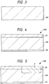
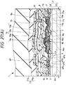
- Fig. 1 is a section showing an essential portion of a semiconductor integrated circuit device according to one embodiment of the present invention
- Fig. 2 is a top plan view of a semiconductor wafer to be used in a process for manufacturing the semiconductor integrated circuit device of Fig. 1
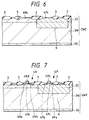
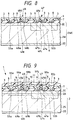
- Figs. 3 to 8 are sections showing an essential portion in a process for manufacturing the semiconductor integrated circuit device of Fig. 1.
- a semiconductor substrate 2 constituting a semiconductor integrated circuit device 1 of the present embodiment 1 is constructed of a semiconductor substrate body 2S, an epitaxial layer (i.e., semiconductor single crystal layer) 2E and a gettering layer (i.e., trap region) 2B.
- an epitaxial layer i.e., semiconductor single crystal layer
- a gettering layer i.e., trap region
- the gettering layer is described, for example, on pp. 42 to 44 of "VLSI TECHNOLOGY", edited by S. M. Sze and issued in 1983 by McGraw-Hill.
- the semiconductor substrate body 2S is made of a single crystal of p ⁇ -type silicon (Si) having a thickness of about 500 to 800 ⁇ m, for example.
- the semiconductor substrate body 2S is doped with a p-type impurity such as boron (B) in a concentration of about 1.3 x 10¹⁵ atoms/cm3.
- the epitaxial layer 2E which is made of a single crystal of p ⁇ -type Si, for example.
- This epitaxial layer 2E is doped with a p-type impurity such as boron in a concentration equal to the designed one of the semiconductor substrate body 2S, e.g., 1.3 x 10¹⁵ atoms/cm3.
- the designed impurity concentration is intended to cover an allowable value.
- the equality to the designed impurity concentration means that, in case the semiconductor substrate body 2S has its designed impurity concentration expressed by [impurity concentration: A] ⁇ (allowable value: ⁇ ] and has an actual impurity concentration of A, the semiconductor substrate body 2S and the epitaxial layer 2E have equal impurity concentrations if the actual impurity concentration of the epitaxial layer 2E is not at A but within A ⁇ ⁇ .
- the p ⁇ -type epitaxial layer 2E is formed over the relatively lightly doped p ⁇ -type semiconductor substrate body 2S, and any precious heavily doped p+-type semiconductor substrate body is not used so that the cost for the semiconductor substrate 2 can be reduced to one half or so.
- the cost for the semiconductor substrate of the prior art having the p ⁇ -type epitaxial layer formed over the p+-type semiconductor substrate body for example, is 2.5 to 3 times as high as that of the ordinary semiconductor substrate having no epitaxial layer.
- the cost for the semiconductor substrate of the present embodiment 1 can be suppressed within 1.5 times as high as that of the ordinary semiconductor substrate. As a result, the cost for the semiconductor integrated circuit device can be lowered.
- the epitaxial layer 2E is made relatively thin to have a thickness of about 1 ⁇ m. As a result, the following effects can be attained.
- the filming apparatus for forming the epitaxial layer is not required to have a high filming accuracy so that it need not be expensive.
- the epitaxial layer can be easily formed to improve the throughput.
- the lower limit of the thickness of the epitaxial layer 2E is one half or more of the thickness of the gate insulating film in the later-described MOS ⁇ FET. This setting is made while considering that one half of the thickness of the gate insulating film of the MOS ⁇ FET goes into the side of the semiconductor substrate 2 when the gate insulating film is formed.
- the epitaxial layer 2E is made thinner than one half of the thickness of a gate insulating film, its entirety is covered with the gate insulating film when this film is to be formed over the epitaxial layer 2E.
- the structure is made such that the gate insulating film is formed over the semiconductor substrate body 2S. This structure loses the effect of the case, in which the gate insulating film is formed over the epitaxial layer 2E, namely, that an excellent gate insulating film can be formed to improve its breakdown voltage.
- the lower limit of the thickness of the epitaxial layer 2E is frequently set to 0.3 ⁇ m by evaluating the performance of the gate insulating film (e.g., the gate breakdown voltage), as will be described with reference to Fig. 25.
- the gate insulating film e.g., the gate breakdown voltage
- the upper limit of the thickness of the epitaxial layer 2E cannot be generally said because it depends upon the product or manufacturing conditions, but may desirably be less than 5 ⁇ m, for example, if the following is considered.
- the upper surface of the epitaxial layer 2E can retain flatness. If the epitaxial layer 2E is made thicker, the level difference of the principal surface of the semiconductor substrate body 2S is accordingly increased, but no substantial difference is caused by the thickness of such extent.
- the principal surface has an excessively large roughness, a larger level difference than the focal depth may be made in a photolithography for the later-described MIS device forming step, thus causing a problem that the pattern cannot be formed by the photolithography.
- the cost for the mother material of the semiconductor substrate 2 or the semiconductor wafer i.e., the later-described epitaxial wafer
- the cost for the mother material of the semiconductor substrate 2 or the semiconductor wafer can be suppressed within a low price. If the epitaxial layer 2E is thickened, it is difficult to control the filming operation, as described above, so that the cost for the semiconductor wafer (i.e., the later-described epitaxial wafer) rises. However, this thickness will not invite a drastic increase in the cost.
- the roughness, if any, on the principal surface of the semiconductor substrate body 2S can be ignored. With the thickness of this order, the roughness will not make a large level difference.
- the epitaxial layer is to be formed over the semiconductor wafer (i.e., the later-described mirror wafer)
- any roughness i.e., crown
- the roughness called the crown will be formed in the vicinity of the outer periphery of the principal surface of the semiconductor wafer (i.e., the later-described mirror wafer). With the thickness of that order, the roughness is not formed (or can be ignored).
- the thickness of the epitaxial layer 2E is preferred to range from 0.3 ⁇ m to 5 ⁇ m.
- the range of 0.3 ⁇ m to 3 ⁇ m is frequently employed, and the optimum range is from 0.3 ⁇ m to 1.0 ⁇ m.
- a field insulating film 3 which is made of silicon dioxide (SiO2), for example.
- a channel stopper region is formed below the field insulating film 3, although not shown.
- the element forming region, as enclosed by the field insulating film 3, is formed, for example, with an n-channel MOS ⁇ FET (as will be shortly referred to as "nMOS”) 4N and a p-channel MOSFET (as will be shortly referred to as "pMOS”) 4P, and these nMOS 4N and pMOS 4P constitute a CMOS (i.e., Complementary Metal Oxide Semiconductor) circuit.
- CMOS Complementary Metal Oxide Semiconductor
- both the nMOS 4N and the pMOS 4P are given an ordinary MOS ⁇ FET structure but should not be limited thereto and may be made of MOS ⁇ FETs having the LDD (i.e., Lightly Doped Drain) structure.
- LDD Lightly Doped Drain
- the nMOS 4N has the following components. Specifically, the nMOS 4N is composed of: a pair of semiconductor regions 4Na and 4Nb formed over the epitaxial layer 2E and apart from each other; a gate insulating film 4Nc formed over the epitaxial layer 2E; and a gate electrode 4Nd formed over the gate insulating film 4Nc.
- the semiconductor regions 4Na and 4Nb are regions for forming the source-drain regions of the nMOS 4N.
- the semiconductor regions 4Na and 4Nb are doped with an n-type impurity such as phosphor (P) or arsenic (As) in a concentration ( dose) of about 1 x 10¹⁵ atoms/cm2.
- the semiconductor regions 4Na and 4Nb are made as deep as about 0.5 ⁇ m and formed in the range of the thickness of the epitaxial layer 2E.
- the gate insulating film 4Nc is made of SiO2 having a thickness of about 18 nm, for example, and formed over the epitaxial layer 2E. As a result, the following effects can be achieved.
- the gate insulating film 4Nc of the MOS.FET over the semiconductor single crystal layer 2E formed of the epitaxial layer 2E, the gate insulating film 4Nc having an excellent film quality can be formed, as described above, to improve its breakdown voltage.
- the defect density (i.e., the number of defects to be caused within a predetermined range) of the gate insulating film 4Nc can be improved ( reduced) by one figure or more.
- the gate electrode 4Nd is made of a single layer film of poly-silicon having a low resistance, for example.
- the gate electrode 4Nd is not limited to the single layer film of poly-silicon of low resistance but can be modified in various manners.
- the gate electrode 4Nd may be constructed by laminating a silicide film of tungsten silicide (WSi2) over the poly-silicon film of low resistance.
- a semiconductor region 5Sa formed over the epitaxial layer 2E is a region for setting the substrate potential at the side of the nMOS 4N.
- This semiconductor region 5Sa is doped with a p-type impurity such as boron in a concentration ( dose) of about 1 x 10¹⁵ atoms/cm2.
- the nMOS 4P is formed in an n-well 6 which is formed over the semiconductor substrate 2.
- the n-well 6 is doped with an n-type impurity such as phosphor or arsenic in a concentration ( dose) of 1 x 10¹³ atoms/cm2.
- the n-well 6 is as deep as about 1.5 ⁇ 4 ⁇ m and extends deeper than the epitaxial layer 2E.
- the n-well 6 is formed in the epitaxial layer 2E and the semiconductor substrate body 25 to have a larger depth than the film thickness of the epitaxial layer 2E.
- the pMOS 4P has the following components. Specifically, the pMOS 4P is composed of: a pair of semiconductor regions 4Pa and 4Pb formed over the epitaxial layer 2E and apart from each other; a gate insulating film 4Pc formed over the epitaxial layer 2E; and a gate electrode 4Pd formed over the gate insulating film 4Pc.
- the semiconductor regions 4Pa and 4Pb are regions for forming the source-drain regions of the pMOS 4P.
- the semiconductor regions 4Pa and 4Pb are doped with an p-type impurity such as boron in a concentration ( dose) of about 1 x 10¹⁸ atoms/cm2.
- the semiconductor regions 4Pa and 4Pb are made as deep as about 0.5 ⁇ m and formed in the range of the thickness of the epitaxial layer 2E.
- the gate insulating film 4Pc is made of SiO2 having a thickness of about 18 nm, for example, and formed over the epitaxial layer 2E. As a result, the same effects as those of the pMOS 4N can be achieved.
- the gate insulating film 4Pc having an excellent film quality can be formed, to improve its breakdown voltage.
- the defect density of the gate insulating film 4Pc can be improved (or reduced) by one figure or more.
- the gate electrode 4Pd is made of a single layer film of poly-silicon having a low resistance, for example.
- the gate electrode 4Pd is not limited to the single layer film of poly-silicon of low resistance but can be modified in various manners.
- the gate electrode 4Pd may be constructed by laminating a silicide film of WSi2 over the polysilicon film of low resistance.
- a semiconductor region 5Sb formed over the epitaxial layer 2E is a region for setting the substrate potential at the side of the pMOS 4P.
- This semiconductor region 5Sb is doped with an n-type impurity such as phosphor or arsenic in a concentration ( dose) of about 1 x 10¹⁸ atoms/cm2.
- an insulating film 7 which is made of SiO2, for example.
- This insulating film 7 is formed in predetermined positions with connection holes 8 for exposing the semiconductor regions 4Na and 4Nb of the nMOS 4N, the semiconductor regions 4Pa and 4Pb of the pMOS 4P, and the semiconductor regions 5Sa and 5Sb for the substrate potential to the outside.
- the semiconductor regions 4Na and 4Nb of the aforementioned nMOS 4N are electrically connected with electrodes 9Na and 9Nb, respectively, through the connection holes 8.
- the semiconductor regions 4Pa and 4Pb of the pMOS 4P are electrically connected with electrodes 9Pa and 9Pb, respectively, through the electrodes 8.
- the semiconductor region 4Nb of the nMOS 4N is electrically connected with the semiconductor region 4Pb of the pMOS 4P through a first-layer wiring line 10 connecting the electrodes 9Nb and 9Pb.
- the semiconductor regions 5Sa and 5Sb for the substrate potential are electrically connected with electrodes 9Sa and 9Sb, respectively, through the connection holes 8.
- Electrodes 9Na, 9Nb, 9Pa, 9Pb, 9Sa and 9Sb and first-layer wiring line 10 are made of an alloy of aluminum (A l )-Si-Copper (Cu), for example.
- a surface protecting film 11 which is formed by laminating a SiO2 film and a silicon carbide (Si3N4) sequentially from the lower layer, for example.
- the surface protecting film 11 covers the electrodes 9Na, 9Nb, 9Pa, 9Pb, 9Sa and 9Sb and the first-layer wiring line 10.
- the semiconductor substrate 2 is formed on its back with a gettering layer 2G.
- This gettering layer 2G is a functional layer for trapping a heavy metal element such as iron (Fe), nickel (Ni), Cu or chromium (Cr) and is formed by covering the back of the semiconductor substrate 2 with a semiconductor film of poly-silicon, for example.
- a (not-shown) column-shaped p ⁇ -type Si single crystal having a crystal face of ⁇ 100 ⁇ azimuth is prepared by the Czochralski method.
- the impurity to be used is exemplified by a p-type impurity such as boron in a concentration of about 1.3 x 10¹⁵ atoms/cm3.
- the slices have their principal surfaces mirror-polished by the chemical-mechanical polishing method or the like to prepare a mirror wafer 2W, as shown in Figs. 2 and 3.
- the mirror wafer 2W is the mother material of the aforementioned semiconductor substrate body 2S.
- the poly-silicon is deposited on the back of the mirror wafer 2W, as shown in Fig. 4, by the CVD (i.e., Chemical Vapor Deposition) method to form the gettering layer 2G.
- This gettering layer 2G is a functional layer for trapping a heavy metal element.
- the epitaxial layer 2E which is made of a p ⁇ -type Si single crystal as thin as about 1 ⁇ m, is formed over the principal surface (as located at the mirror surface side) of the mirror wafer 2W by the CVD method (e.g., the epitaxial growth method) of about 980°C, for example, by using monosilane (SiH4) gas and hydrogen (H2) gas, thereby to manufacture an epitaxial wafer (or semiconductor wafer) 2WE.
- the CVD method e.g., the epitaxial growth method
- SiH4 monosilane
- H2 hydrogen
- the impurity concentration in the epitaxial layer 2E is set equal to the designed one of the mirror wafer 2W.
- the epitaxial layer 2E is doped with a p-type impurity such as boron in a concentration of about 1.3 x 10¹⁵ atoms/cm3.
- the not-shown ion implantation mask is formed over the epitaxial wafer 2WE and is then used to dope a predetermined position of the epitaxial wafer 2WE, as shown in Fig. 5, with an n-type impurity such as phosphor or arsenic by the ion implantation method. After this, the epitaxial wafer 2WE is subjected to a heat treatment to form the n-well 6.
- n-well 6 An ion implantation impurity concentration (dose) for forming that n-well 6 is at about 1 x 10¹³ atoms/cm2 and is as deep as about 1.5 to 4 ⁇ m and deeper than the epitaxial layer 2E.
- the field insulating film 3 made of SiO2 or the like is formed over the principal surface of the epitaxial layer 2E by the LOCOS method or the like. After this, the element forming region, as enclosed by the field insulating film 3, is simultaneously formed with the gate. insulating films 4Nc and 4Pc made of SiO2 or the like having a thickness of about 180 angstroms by the thermal oxidation method or the like.
- the gate insulating films 4Nc and 4Pc can be formed to have an excellent film quality by forming them over the epitaxial layer 2E so that their breakdown voltages can be improved. Moreover, the gate insulating films 4Nc and 4Pc can have their defect densities improved by one figure or more.
- the gate insulating films 4Nd and 4Pd of poly-silicon having a low resistance are simultaneously formed over the gate insulating films 4Nc and 4Pc.
- the gate insulating films 4Nd and 4Pd are used as masks to form the paired gate insulating films 4Na and 4Nb and the paired gate insulating films 4Pa and 4Pb by different ion implantation steps, to form the nMOS 4n and pMOS 4P over the epitaxial wafer 2WE.
- the semiconductor regions 5Sa and 5Sb are separately formed in predetermined positions of the epitaxial layer 2E.
- the insulating film 7 made of SiO2, for example, is deposited over the epitaxial wafer 2WE by the CVD method or the like.
- the insulating film 7 is formed with the connection holes 8 to expose the semiconductor regions 4Na and 4Nb of the nMOS 4N, the semiconductor regions 4Pa and 4Pb of the pMOS 4P and the semiconductor regions 5SA and 5Sb for the substrate potential to the outside.
- the conductor film 9 is patterned by the dry etching method or the like to simultaneously form the electrodes 9Na, 9Nb, 9Pa, 9Pb, 9Sa and 9Sb and the first wiring line 10, as shown in Fig. 1.
- the surface protecting film 11 is formed over the epitaxial wafer 2WE by sequentially depositing the insulating film of SiO2 and the insulating film of Si3N4, for example, by the CVD method or the like. After this, the epitaxial wafer 2WE is divided into individual semiconductor chips to manufacture the semiconductor integrated circuit device 1, as shown in Fig. 1.
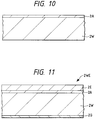
- Fig. 9 is a section showing an essential portion of a semiconductor integrated circuit device according to another embodiment of the present invention
- Figs. 10 and 11 are sections showing an essential portion at steps of manufacturing the semiconductor integrated circuit device of Fig. 9.
- the present embodiment 2 is different from the embodiment 1 in that the semiconductor substrate body 2S is formed over its principal surface with a non-defective layer 2A, which is formed thereover with the epitaxial layer 2E.
- the non-defective layer 2A is in the state having substantially neither any structural defect (e.g., the stacking fault or the dislocation loop) nor any precipitation of oxygen, of which the former is substantially zero whereas the latter is at about 0.1 cm ⁇ 2, when observed by the light scattering method.
- the non-defective layer 2A is made of a p ⁇ -type Si single crystal which have an impurity content and a concentration equal to those of the semiconductor substrate body 2S.
- the mirror wafer 2W is prepared as in the foregoing embodiment 1. After this, the mirror wafer 2W is heated at a temperature (e.g., at about 1,100°C to 1,200°C for 10 to 60 minutes) in the H2 gas atmosphere, for example, to form the non-defective layer 2A over the principal surface of the mirror wafer 2W.
- a temperature e.g., at about 1,100°C to 1,200°C for 10 to 60 minutes
- poly-silicon for example, is deposited on the back of the mirror wafer 2W by the CVD method or the like to form the gettering layer 2G.
- This gettering layer 2G is a functional layer for trapping a heavy metal element.
- the epitaxial layer 2E made of a p ⁇ -type Si single crystal having a relatively small thickness of about 1 ⁇ m, for example, is formed over the non-defective layer 2A by the CVD method (e.g., the epitaxial growth method) using SiH4 gas and H2 gas, for example.
- the impurity and its concentration in the epitaxial layer 2E are similar to those of the foregoing embodiment 1.
- the subsequent steps are similar to those of the aforementioned embodiment 1, and their description will be omitted.
- the epitaxial layer 2E can be improved in its crystal growth to reduce the defects and dislocations drastically. As a result, it is possible to further improve the production yield, performance and reliability of the semiconductor integrated circuit device.
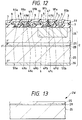
- Fig. 12 is a section showing an essential portion of a semiconductor integrated circuit device according to another embodiment of the present invention
- Figs. 13 to 15 are sections showing an essential portion in the steps of manufacturing the semiconductor integrated circuit device of Fig. 12.
- a p+-type semiconductor region i.e., a heavily doped semiconductor region
- the p+-type semiconductor region 2B is doped with a p-type impurity such as boron in a higher concentration of about 1 x 10¹⁸ atoms/cm3 than that of the epitaxial layer 2E or the semiconductor substrate body 2S.
- the p+-type semiconductor region 2B is a functional layer for suppressing the latchup of the CMOS circuit. Specifically, in the present embodiment 3, the p+-type semiconductor region 2B is formed so that the resistance of the surface layer side of the substrate can be drastically lowered to improve the resistance of the CMOS circuit to the latchup.
- the epitaxial layer 2E is thicker at about 5 ⁇ m than those of the foregoing embodiments 1 and 2.
- the lower limit of the thickness of the epitaxial layer 2E is set to a deeper value than that of the n-well 6 in the pMOS forming region.
- the p+-type semiconductor region 2B is formed in the n-well 6 to make it difficult to set the impurity concentration in the n-well 6 if the thickness of the epitaxial layer 2E is made smaller than the depth of the n-well 6.
- the upper limit of the thickness of the epitaxial layer 2E may desirably be less than 5 ⁇ m. This is reasoned as in the foregoing embodiment 1. However, the thickness may exceed that value so long as an increase in the cost is allowed.
- the mirror wafer 2W is prepared as in the foregoing embodiment 1.
- the mirror wafer 2W (or the semiconductor substrate body 2S) is highly accurately doped with a p-type impurity such as boron to a predetermined depth (e.g., about 1 ⁇ m) from its principal surface.
- the impurity concentration at this time is about 1 x 10¹⁸ atoms/cm3.
- the mirror wafer 2W is thermally treated to form the p+-type semiconductor region 2B.
- a poly-silicon for example, is deposited on the back of the mirror wafer 2W by the CVD method or the like to form the gettering layer 2G.
- This gettering layer 2G is a functional layer for trapping a heavy metal element.
- the epitaxial layer 2E (or the semiconductor single crystal layer) made of a p ⁇ -type Si single crystal having a thickness of about 5 ⁇ m, for example, is formed over the principal surface (as located at the mirror surface side) of the mirror wafer 2W, as shown in Fig. 14, by the CVD method (i.e., the epitaxial growth method) using SiH4 and H2 gas, for example, to form the epitaxial wafer 2WE.
- the impurity concentration in the epitaxial layer 2E is set to be equal to the designed one of the mirror wafer 2W.
- the epitaxial layer 2E is doped with a p-type impurity such as boron, for example, in a concentration of about 1.5 x 10¹⁵ atoms/cm3.
- the not-shown ion implantation mask is formed over the epitaxial wafer 2WE and is then used as a mask to dope a predetermined position of the epitaxial wafer 2WE, as shown in Fig. 15, with an n-type impurity such as phosphor or boron by the ion implantation method. After this, the epitaxial wafer 2WE is subjected to a heat treatment to form the n-well 6.
- the n-well 6 has a depth of about 3 ⁇ m and is formed in the epitaxial layer 2E.
- the ion implantation impurity concentration ( dose) for forming that n-well 6 is at about 1 x 10¹³ atoms/cm2.
- the subsequent steps are similar to those of the aforementioned present embodiment 1 so that their description will be omitted.
- the resistance at the side of the substrate surface can be drastically lowered to improve the resistance of the CMOS circuit to the latchup. As a result, it is possible to further improve the performance, reliability and production yield of the semiconductor integrated circuit device.
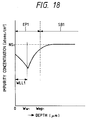
- Fig. 16 is a section showing an essential portion of a semiconductor integrated circuit device according to another embodiment of the present invention
- Fig. 17 is an impurity distribution diagram in the semiconductor integrated circuit device of Fig. 16
- Figs. 18 and 19 are impurity distribution diagrams in the semiconductor integrated circuit device having been described in the prior art
- Figs. 20 to 24 are sections showing an essential portion in the steps of manufacturing the semiconductor integrated circuit device
- Fig. 25 is a graph for explaining the effects of the semiconductor integrated circuit device of the present embodiment.
- the portions identical to those of the foregoing embodiment 1 are designated at the common reference characters.
- the relatively lightly doped semiconductor substrate body 2S constituting the semiconductor integrated circuit device 1 of the present embodiment 4 is made of a p-type Si single crystal or the like, for example.
- the semiconductor substrate body 2S is doped with a p-type impurity such as boron in a concentration of about 1.5 x 10¹⁵ atoms/cm3.
- the semiconductor substrate body 2S is formed over its principal surface with the epitaxial layer 2E made of a p ⁇ -type Si single crystal or the like.
- the epitaxial layer 2E is doped with a p-type impurity such as boron in a concentration lower than the designed one of the semiconductor substrate body 2S.
- the p ⁇ -type epitaxial layer 2E is formed over the p-type semiconductor substrate body 2S as in the foregoing embodiment 1 so that the expensive p+-type semiconductor substrate body need not be used to lower the cost for the semiconductor substrate 2 to about one half.
- the impurity concentration of the semiconductor substrate body 2S is made higher than that of the epitaxial layer 2E, the resistance of the semiconductor substrate body 2S can be made lower than that of the epitaxial layer 2E to improve the resistance to the latchup.
- the epitaxial layer 2E has a thickness W E (from the surface of the epitaxial layer 2E) similar to that of the foregoing embodiment 1, as exemplified by about 1 ⁇ m. As a result, it is possible to achieve the same effects as those described in connection with the foregoing embodiment 1.
- the upper and lower limits of the thickness of the epitaxial layer 2E are similar to those of the foregoing embodiment 1.
- the semiconductor substrate 2 is formed in its upper portion with a p-well (i.e., the first semiconductor region) 6p and an n-well (i.e., the first semiconductor region) 6n.
- the p-well 6p is doped with a p-type impurity such as boron.
- the p-well 6p is formed with the nMOS 4N.
- the n-well 6n is doped with an n-type impurity such as phosphor.
- the n-well 6n is formed with the pMOS 4P.
- the depth W W i.e., the depth from the surface of the epitaxial layer 2E
- the n-well 6p is larger than the thickness W E of the epitaxial layer 2E.
- the CMOS circuit is constructed of the nMOS 4N and the pMOS 4P, which have their structures, materials and effects similar to those of the foregoing embodiment 1.
- the structures of the nMOS 4N and the pMOS 4P may be changed to the double drain (or double diffused drain) structure and the LDD (i.e., Lightly Doped Drain) structure.
- insulating film 7 On the insulating film 7, there is deposited an insulating film 7a of SiO2, for example, on which is deposited a flattening insulating film 7b.
- the insulating films 7, 7a and 7b are formed with connection holes 8a extending to reach the electrodes 9Nb and 9Pb, through which a second-layer wiring line 10a is electrically connected with the electrodes 9Na and 9Pa.
- the second-layer wiring line 10a is formed by depositing a barrier layer 10a1 of titanium nitride (TiN), a conductor layer 10a2 of an A l -Si-Cu alloy and a barrier layer 10a3 of titanium nitride sequentially from the lower layer.
- the aforementioned p-well 6p and n-well 6n are formed to extend from the surface of the epitaxial layer 2E to the upper portion of the semiconductor substrate body 2S, as shown in Figs. 16 and 17, and the p-well 6p and n-well 6n have their impurity concentrations gradually lowered in the depthwise direction from the principal surface (having an impurity concentration N W ) of the epitaxial layer 2E.
- the impurity concentration of the p-well 6p is given such a gradient that it is gradually lowered in the depthwise direction from the surface of the epitaxial layer 2E, so that the influence to be caused by the carriers (or electrons) due to the ⁇ -ray is lowered.
- the electrons produced by the ⁇ -ray are attracted to the substrate body 2S by that concentration gradient and prevented from entering the p-well 6p so that the soft errors can be reduced in case the MIS memory of the DRAM or the like is formed in the p-well 6p.
- the impurity concentration N W in the principal surface of the epitaxial layer 2E of the p-well 6p and the n-well 6n is at about 6 x 10¹⁶ atoms/cm3, so that the impurity concentration of the p-well 6p and the n-well 6n is at 5 x 10¹⁵ to 6 x 10¹⁶ atoms/cm3.
- letter A plots the impurity concentration distributions of the epitaxial layer 2E and semiconductor substrate body 2S in the epitaxial wafer state, and indicates that the impurity concentration (N E ) of the epitaxial layer 2E is lower than that (N S ) of the semiconductor substrate body 2S, as described above.
- the p-well 6p is formed after the p ⁇ - type epitaxial layer 2E is formed over the p-type semiconductor substrate body 2S, the well concentration (i.e., the concentration N W of the well surface) of the p-well 6p is not influenced by the p-type impurity concentration of the semiconductor substrate body 2S.
- the well concentration N W of the p-well 6p is not influenced by the dispersion of the p-type impurity concentration of the semiconductor substrate body 2S so that the fluctuation of the Vth of the MIS ⁇ FET is not caused by that dispersion.
- the allowable concentration range can be widened more than the prior art with respect to the dispersion of the p-type impurity concentration of the semiconductor substrate body 2S so that the cost for the semiconductor integrated circuit device can be lowered.
- only a narrow range can be used as the p-type impurity concentration of the semiconductor substrate body 2S to raise the cost for the semiconductor integrated circuit device.
- Figs. 18 and 19 corresponds to the case of the aforementioned technique, as described on pp. 761 to 763 of "Applied Physics, Vol. 60, No. 8", issued on August 10, 1991, by Japanese Association of Applied Physics
- Fig. 19 corresponds to the case of the aforementioned technique, as described in the Japanese Patent Laid-Open No. 260832/1989.
- the impurity concentration NS1 of the semiconductor substrate body SB1 is higher than that of the epitaxial layer EP1.
- the well WLL1 is formed in the epitaxial layer from the standpoint of setting the impurity concentration. This makes it necessary to make the epitaxial layer deeper, as at Wep1, than the well WLL1.
- the thickness Wep1 of the epitaxial layer has to be larger than the depth of the well WLL1.
- the well WLL1 of this case is formed by implanting the epitaxial layer EP1 with the impurity from the surface thereof, so that the impurity concentration is higher in the substrate surface than in the inside.
- the impurity concentrations of both the semiconductor substrate body SB2 and the epitaxial layer EP2 are set to be low, as at NS2.
- the well WLL2 is formed to extend deeper, as at W W2 , than the depth Wep2 of the epitaxial layer EP2.
- the well WLL2 of this case is formed by the diffusion (i.e., the diffusion of the impurity of the semiconductor substrate body SB2 from the semiconductor substrate body to the epitaxial layer EP2) at the time when the epitaxial layer EP2 is formed over the semiconductor substrate body SB2 which has been doped in its upper portion with a well forming impurity.
- the impurity concentration is low, as at NS3, in the substrate surface but high, as at NS4, in the boundary region between the epitaxial layer EP2 and the semiconductor substrate body SB2 and gets lower internally of the semiconductor substrate body.
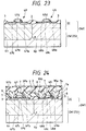
- the mirror wafer 2W or the mother material of the semiconductor substrate body 2S made of a p-type Si single crystal is formed over its mirror surface with the epitaxial layer 2E, which is made of an Si single crystal having the same conduction type as the mirror wafer 2W and containing an impurity of a lower concentration than that of the mirror wafer 2W, by the CVD method using SiH4 gas and H2 gas similar to those of the foregoing embodiment 1.
- the mirror wafer 2W has an impurity concentration of about 1.5 x 10¹⁵ atoms/cm3.
- the epitaxial layer 2E has a thickness W E of about 1 ⁇ m, for example.
- the mirror wafer 2W is formed in its predetermined region with an insulating film 12a made of SiO2 having a thickness of about 40 nm.
- the film portion in the n-well forming region is removed from the insulating film of Si3N4 by the dry etching method or the like.
- the film portion and the resist film of the p-well forming region in the insulating film of Si3N4 is used as a mask to dope the exposed portion of the epitaxial layer 2E with the ions of an n-type impurity such as phosphor for forming the n-well.
- the ion implanting energy at this time is at about 125 KeV, and the dose is about 2 x 10¹³ atoms/cm2.
- the film portion, as in the p-well forming region, of the insulating film of Si3N4 is used as a mask to form an insulating film 12b having a thickness of about 120 nm over the epitaxial layer 2E at the n-well side.
- the insulating film over the n-well forming region is used as an ion implantation mask to dope the exposed portion of the epitaxial layer 2E with a p-type impurity such as boron for forming the p-well, for example.
- the ion implantation energy at this time is about 60 KeV, and the dose is about 8 x 10¹² atoms/cm2, for example.
- the mirror wafer 2W is subjected to an annealing treatment for extended diffusion for 3 hours, for example, to form the p-well 6p and the n-well 6n having a depth of about 3 ⁇ m, for example.
- the treatment temperature at this time is about 1,200°C, for example.
- the p-well 6p and the n-well 6n are extended from the surface of the epitaxial layer 2E to the upper portion of the mirror wafer 2W and made to have their impurity concentrations gradually lowered depthwise from the surface of the epitaxial layer 2E.
- the impurity concentration of the p-well 6p and the n-well 6n is at 5 x 10¹⁵ to 6 x 10¹⁶ atoms/cm3.
- a pad oxide film 12c and the (not-shown) non-oxidizable insulating film of Si3N4 are deposited sequentially from the lower layer. After this, the non-oxidizable insulating film is removed from the element separating region but left at the element forming region.
- the non-oxidizable insulating film left unremoved is used as a mask to form the field insulating film 3 selectively in the element separating region.
- the element forming region, as enclosed by the field insulating film 3 is formed by the thermal oxidation method with the gate insulating films 4Nc and 4Pc made of SiO2 having a thickness of about 180 angstroms, for example.
- the gate insulating films 4Nc and 4Pc are given an excellent film quality by forming them over the epitaxial layer 2E so that their breakdown voltages can be improved. Moreover, the gate insulating films 4Nc and 4Pc can have their defect densities improved by one figure or more.
- the gate insulating films 4Nc and 4Pc are simultaneously formed thereover with the gate electrodes 4Nd and 4Pd made of an n-type poly-silicon of low resistance, for example.
- these gate electrodes 4Nd and Pd are used as masks to form the paired semiconductor regions 4Na and 4Nb and the paired semiconductor regions 4Pa and 4Pb by the separate ion implantation steps thereby to form the nMOS 4N and pMOS 4P over the epitaxial wafer 2WE.
- the gate electrodes 4Nd and 4Pd should not be limited to those made of elemental poly-silicon but can be modified in various manners.
- the gate electrodes 4Nd and 4Pd may be given the so-called "poly-cide structure", in which a refractory metal silicide film is deposited on poly-silicon of low resistance.
- the semiconductor region 4Na of the nMOS 4N is formed by doping it with ions of As in a dose of about 1 x 10¹⁵ atoms/cm2, for example.
- the semiconductor region 4Pa of the pMOS 4P is formed by doping it with ions of BF2 in a dose of about 1 x 10¹⁵ atoms/cm2, for example.
- the semiconductor regions 4Na, 4Nb, 4Pa and 4Pb may be exemplified by the double diffused drain structure or the LDD structure, as described above.
- the insulating film 7 of SiO2 is deposited on the epitaxial wafer 2WE by the CVD method or the like.
- This insulating film 7 is mainly composed of the BPSG (i.e., Boro Phospho Silicate Glass) containing B2O3 and P2O5.
- the insulating film 7 is formed with the connection holes 8 for exposing the semiconductor regions 4Na and 4Nb of the nMOS 4N and the semiconductor regions 4Pa and 4Pb of the pMOS 4P to the outside.
- the conductor film 9 of the A l -Si-Cu alloy for example, is deposited on the epitaxial wafer 2WE by the sputtering method or the evaporation method.
- the conductor film 9 is patterned by the dry etching method or the like to form the electrodes 9Na, 9Nb, 9Pa, 9Pb, 9Sa and 9Sb.
- the insulating film 7a of SiO2 for example, is deposited on the epitaxial wafer 2WE by the CVD method of the like.
- the flattening insulating film 7b of SiO2 is deposited on the insulating film 7a by the CVD method or the like.
- the flattening insulating film 7b is flattened by the CMP (i.e., Chemical Mechanical Polishing) method or the like. After this, the insulating films 7, 7a and 7b are formed with the connection holes 8a by the dry etching method, as shown in Fig. 16.
- CMP Chemical Mechanical Polishing
- the barrier layer 10a1 of TiN, the conductor layer 10a2 of the A l -Si-Cu alloy and the barrier layer 10a3 of TiN are deposited on the epitaxial wafer 2WE sequentially from the lower layer by the sputtering method or the evaporation method.
- barrier layers 10a1 and 10a3 and conductor layer 10a2 are patterned by the dry etching method or the like to form the second-layer wiring line 10a.
- the insulating film 7c of SiO2, for example, is deposited on the epitaxial wafer 2WE by the CVD method or the like.
- the insulating film 11a of SiO2 is deposited on the insulating film 7c by the CVD method or the like.
- the insulating film 11b of Si3N4 is then deposited on the insulating film 11a by the CVD method or the like to from the surface protecting film 11.
- the individual semiconductor chips are divided from the epitaxial wafer 2WE to manufacture the semiconductor integrated circuit device 1, as shown in Fig. 16.
- Fig. 25 plots the performances of the gate insulating film in case the MOS capacitor to have its gate breakdown voltage evaluated is prepared after the process for manufacturing the 4M ⁇ DRAM is executed to the step of forming the gate insulating film.
- the gate insulating film has a thickness of about 18 nm; the gate electrode has an area of about 4.8 mm2; and the gate electrode is made of phosphor-doped poly-silicon.
- the abscissa indicates the thickness W E of the epitaxial layer.
- the ordinate indicates the defect density which is calculated from the following equation by measuring the breakdown characteristics of about two hundreds of MOS capacitors on the semiconductor wafer (or the epitaxial wafer) and then by deciding the non-defective and defective produces according to the following standards.
- the densities are generally indicated in relative values with reference to the mirror wafer for the MOS ⁇ LSI having no epitaxial layer.
- the defect density can be reduced more by one figure or more than the case, in which the gate insulating film is formed over the mirror wafer, to provide an excellent gate breakdown performance.
- Fig. 26(A) is a section showing an essential portion of a semiconductor integrated circuit device according to another embodiment of the present invention.
- the semiconductor integrated circuit device 1 of the present embodiment 5, as shown in Fig. 26(A), is exemplified by a 16M ⁇ DRAM.
- Fig. 16(B) is a circuit diagram showing a memory cell of the DRAM.
- the lefthand side shows a memory cell region
- the righthand side shows a peripheral circuit region.
- this peripheral circuit region has the same structure as that of the foregoing embodiment 4, and its description will be omitted.
- the impurity concentration of the epitaxial layer 2E is made lower than that of the semiconductor substrate body 2S, as in the foregoing embodiment 4.
- one memory cell MC is constructed one transfer MOS.FET 13 and one capacitor 14.
- the transfer MOS ⁇ FET 13 is composed of a pair of semiconductor regions 13a and 13b formed in a p-well 6p1, a gate insulating film 13c formed over the epitaxial layer 2E, and a gate electrode 13d formed over the gate insulating film 13c.
- the p-well 6p1 is formed to extend from the surface of the epitaxial layer 2E to the upper portion of the semiconductor substrate body 2S, as located deeper than the epitaxial layer 2E. Moreover, the impurity concentration of the p-well 6p1 is made gradually lower, as in the foregoing embodiment 4, depthwise of the semiconductor substrate 2.
- the paired semiconductor regions 13a and 13b are doped with an n-type impurity such as As.
- these semiconductor regions 13a and 13b are formed in the epitaxial layer 2E having less defects due to the precipitation of oxygen, so that the junction leakage current can be reduced to improve the performance, reliability and production yield of the DRAM.
- bit line 15 is composed, for example, of a conductor layer 15a made of polycrystalline silicon of low resistance and a conductor layer 15b formed over the former and made of tungsten silicide or the like.
- the semiconductor region 13b With the other semiconductor region 13b, on the other hand, there is electrically connected a lower electrode 14a of the capacitor 14.
- the semiconductor region 13b is formed in the epitaxial layer 2E having less defects due to the precipitation of oxygen, so that the leakage of the charge accumulated in the capacitor 14 can be suppressed to elongate the charge storage time period thereby to improve the refresh characteristics.
- the capacitor 14 is formed into a fin shape and constructed of the lower electrode 14a, an upper electrode 14b, and a (not-shown) insulating film interposed between those electrodes.
- the shape of the capacitor should not be limited to the fin but can be modified in various manners such as a cylindrical shape.
- the gate electrode 13d of the transfer MOS.FET 13 also acts as the word line (WL).
- reference numerals 16a and 16b appearing in Fig. 26(A) designate channel stopper regions.
- the semiconductor region 13b to be electrically connected with the lower electrode 14a of the capacitor 14 is formed in the epitaxial layer 2E, the leakage of the charge accumulated in the capacitor 14 can be suppressed to elongate the charge storage time period thereby to improve the refresh level. As a result, it is possible to improve the performance, reliability and production yield of the DRAM.
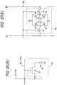
- Fig. 27(A) is a section showing an essential portion of a semiconductor integrated circuit device according to another embodiment of the present invention.
- the semiconductor integrated circuit device 1 of the present embodiment 6, as shown in Fig. 27(A), is exemplified by a 4M ⁇ SRAM (i.e., 4 Megabit Static RAM).
- the impurity concentration of the epitaxial layer 2E is made lower than that of the semiconductor substrate body 2S, as in the foregoing embodiment 4.
- Fig. 27(B) is a circuit diagram showing a memory cell of the SRAM.
- the memory cell region is formed with a p-well 6p2, and the peripheral circuit region is formed with an n-well 6n1.
- p-well 6p2 and n-well 6n1 are formed, as in the foregoing embodiments 4 and 5, to extend from the surface of the epitaxial layer 2E to the upper portion of the semiconductor substrate body 2S. Moreover, their impurity concentrations are made gradually lower depthwise of the semiconductor substrate 2 as in the foregoing embodiment 4.
- the memory cell region is formed with a transfer MOS ⁇ FET 17, a drive MOS ⁇ FET 18 and a load MOS.FET 19.
- the transfer MOS ⁇ FET 17 is composed of: a pair of semiconductor regions 17a and 17b formed in the upper portion of the p-well 6p2; a gate insulating film 17c formed over the epitaxial layer 2E; and a gate electrode 17d formed over the gate insulating film 17c.
- These semiconductor regions 17a and 17b are doped with an n-type impurity such as As.
- One semiconductor region 17a is electrically connected through the first -layer wiring line 10 with the bit line 15 (BL and BL ⁇ ).
- the other semiconductor region 17b is electrically connected with a gate electrode 18d of the drive MOS ⁇ FET 18.
- the transfer MOS ⁇ FET 17 and the drive MOS ⁇ FET 18 have their gate electrodes 17d and 18d formed by depositing a refractory metal silicide on the conductor film made of poly-silicon of low resistance, and the transfer MOS ⁇ FET 17 has its gate electrode 17d connected with the word line WL.
- the gate insulating films 17c and 18c are made of SiO2, for example. Still moreover, the paired semiconductor regions of the drive MOS ⁇ FET 18 are positioned in the direction of the channel length of the gate electrode 18d, although not shown.
- the load MOS ⁇ FET 19 is composed of a gate electrode 19a made of poly-silicon of low resistance, and a pair of semiconductor regions 19c and 19d formed over the gate electrode 19a through a gate insulating film 19b and made of poly-silicon of low resistance.
- the semiconductor regions 19c and 19d are doped with an n-type impurity such as As.
- the peripheral circuit region is formed with the pMOS 4P, for example.
- This pMOS 4P is composed of: the paired semiconductor regions 4Pa and 4Pb formed in the upper portion of the n-well 6n1; the gate insulating film 4Pc formed over the epitaxial layer 2E; and the gate electrode 4Pd formed over the gate insulating film 4Pc.
- These semiconductor region 4Pa and 4Pb are doped with a p-type impurity such as boron.
- the memory cell (MC) of the SRAM is formed over the epitaxial layer 2E having less defects due to the precipitation of oxygen so that the junction leakage current can be reduced in the paired semiconductor regions 17a and 17b of the transfer MOS ⁇ FET 17 and the (not-shown) paired semiconductor regions of the drive MOS ⁇ FET 18, as composing the memory cell (MC).
- the data storage retaining characteristics e.g., the data retention level
- the data retention level can be improved to reduce the data retention fault percentage.
- Fig. 28 is a section showing an essential portion of a semiconductor integrated circuit device according to another embodiment of the present invention.
- the semiconductor integrated circuit device 1 of the present embodiment 7, as shown in Fig. 28, is exemplified by a flash memory (i.e., flash EEPROM (Electrically Erasable Programmable ROM)) capable of electrically erasing/programming data.
- a flash memory i.e., flash EEPROM (Electrically Erasable Programmable ROM)
- the impurity concentration of the epitaxial layer 2E is made lower than that of the semiconductor substrate body 2S.
- the semiconductor substrate 2 is formed thereover with a p-well 6p3 and an n-well 6n2.
- These p-well 6p3 and n-well 6n2 are formed, as in the foregoing embodiments 4 to 6, to extend from the surface of the epitaxial layer 2E to the upper portion of the semiconductor substrate body 2S.
- their impurity concentrations are made gradually deeper depthwise of the semiconductor region 2, as in the foregoing embodiment 4.
- the memory cell region is formed with a memory cell MC1.
- This memory cell MC1 is constructed of a single MOS ⁇ FET.
- the memory cell MC1 is composed of: a pair of semiconductor regions 20a and 20b formed in the upper portion of the p-well 6p3; a gate insulating film 20c formed over the epitaxial layer 2E; a floating gate electrode 20d formed over the gate insulating film 20c; a control gate electrode 20e formed over the floating gate electrode 20d through the (not-shown) insulating film.
- One semiconductor region 20a is composed of a semiconductor region 20a1 and a semiconductor region 20a2 formed in the former.
- the semiconductor region 20a1 is doped with an n ⁇ -type impurity such as phosphor
- the semiconductor region 20a2 is doped with an n+-type impurity such as As.
- the other semiconductor region 20b is composed of a semiconductor region 20b1 and a semiconductor region 20b2 formed in the former.
- the semiconductor region 20b1 is doped with a p+-type impurity such as boron
- the semiconductor region 20b2 is doped with an n+-type impurity such as As.
- the peripheral circuit region is formed with the nMOS 4N and the pMOS 4P, for example.
- the nMOS 4N is composed of: the paired semiconductor regions 4Na and 4Nb formed in the upper portion of the p-well 6p3; the gate insulating film 4Nc formed over the epitaxial layer 2E; and the gate electrode 4Nd formed over the gate insulating film 4Nc.
- These semiconductor regions 4Na and 4Nb are doped with an n-type impurity such as phosphor.
- the pMOS 4P is composed of: the paired semiconductor regions 4Pa and 4Pb formed in the upper portion of the n-well 6n2; the gate insulating film 4Pc formed over the epitaxial layer 2E; and the gate electrode 4Pd formed over the gate insulating film 4Pc.
- These semiconductor regions 4Pa and 4Pb are doped with a p- type impurity such as boron.
- the semiconductor region 4Na of the nMOS 4N and the semiconductor region 4Pa of the pMOS 4P are electrically connected through the first-layer wiring line 10 to construct the CMOS circuit.
- the memory cell of the flash memory i.e., EEPROM
- the memory cell of the flash memory is formed over the epitaxial layer 2E having less defects such as the precipitation of oxygen, so that the breakdown voltage of the gate insulating film 20c can be raised to improve the data programming resistance.
- the erasure dispersion at the time of erasing the data can be reduced. As a result, it is possible to improve the performance, reliability and production yield of the flash memory (i.e., EEPROM).
- the gettering layer is made of poly-silicon.
- the present invention should not be limited thereto but can be modified in various manners.
- the gettering layer may be formed by the method of mechanically forming a working strain on the back of the semiconductor substrate body, the method of properly adjusting or precipitating the oxygen element which is present in the semiconductor substrate body, or the method of doping the semiconductor substrate with carbon ions.
- the structure may be dispensed with the gettering layer.
- the substrate gettering effect can be enhanced by setting the oxygen concentration to about or more than 9 x 10¹⁷ atoms/cm3.
- the gate insulating film can be formed over the epitaxial layer formed over the semiconductor substrate body and containing no oxygen element, thereby to improve the breakdown characteristics of the gate insulating film.
- the oxygen concentration present in the semiconductor substrate body is made as high as 9 x 10¹⁷ atoms/cm3
- the oxygen is precipitated in the aforementioned principal surface so that any clean gate insulating film is not formed to deteriorate the breakdown characteristics of the gate insulating film.
- the oxygen concentration has to be lowered to make the gettering effect insufficient.
- the epitaxial layer is formed by the epitaxial growth method using the SiH4 gas.
- the present invention should not be limited thereto but can be modified in various manners.
- the epitaxial layer may be formed by the epitaxial growth method using silicon tetrachloride (SiC l 4) gas.
- the foregoing embodiments 1, 2 and 4 to 7 have been described in case the semiconductor substrate body and the epitaxial layer are made of p ⁇ -type Si.
- the present invention should not be limited thereto but can be modified such that the semiconductor substrate body and the epitaxial layer are made of n ⁇ -type Si.
- the semiconductor substrate body and the epitaxial layer may be made of n ⁇ -type Si, and the p+-type semiconductor region may be made of n+-type Si.
- the foregoing embodiment 3 has been described in case the p+-type semiconductor region for suppressing the latchup is formed all over the semiconductor substrate body.
- the present invention should not be limited thereto but can be modified in various manners.
- a p+-type semiconductor region may be formed below the CMOS circuit forming region.
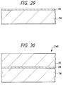
- Fig. 29 shows the case in which the epitaxial layer 2E is formed over the semiconductor substrate body 2S of Fig. 29.
- the non-defective layer of the semiconductor integrated circuit device of the foregoing embodiment 2 may be formed below the epitaxial layer.
- the techniques having been described in connection with the foregoing embodiments 1 to 3 can also be applied to another semiconductor integrated circuit device such as the semiconductor integrated circuit device which has a semiconductor memory circuit such as the flash memory represented by the DRAM, the SRAM or the ROM (Read Only Memory).
- the semiconductor integrated circuit device which has a semiconductor memory circuit such as the flash memory represented by the DRAM, the SRAM or the ROM (Read Only Memory).
- the semiconductor substrate body 2S having a size as large as 12 inches may be useful.
- the present invention has been described in case it is applied to the semiconductor integrated circuit device having the CMOS circuit having the field of application of its background.
- the present invention should not be limited thereto but can be modified in various manners.
- the present invention can be applied to another semiconductor integrated circuit device such as the semiconductor integrated circuit device having the bipolar transistors or the semiconductor integrated circuit device having a BiCMOS circuit composed of the bipolar transistors and the CMOS circuit.
- the MOS ⁇ FET is used, but the present invention should not be limited thereto.
- the MIS ⁇ FET i.e., Metal-Insulator-Semiconductor ⁇ FET
- MOSFET Metal-Insulator-Semiconductor ⁇ FET
- SiN silicon nitride film
Landscapes
- Engineering & Computer Science (AREA)
- Physics & Mathematics (AREA)
- Condensed Matter Physics & Semiconductors (AREA)
- General Physics & Mathematics (AREA)
- Manufacturing & Machinery (AREA)
- Computer Hardware Design (AREA)
- Microelectronics & Electronic Packaging (AREA)
- Power Engineering (AREA)
- Metal-Oxide And Bipolar Metal-Oxide Semiconductor Integrated Circuits (AREA)
- Insulated Gate Type Field-Effect Transistor (AREA)
- Recrystallisation Techniques (AREA)
- Semiconductor Memories (AREA)
Applications Claiming Priority (6)
| Application Number | Priority Date | Filing Date | Title |
|---|---|---|---|
| JP176872/94 | 1994-07-28 | ||
| JP17687294 | 1994-07-28 | ||
| JP17687294 | 1994-07-28 | ||
| JP6265529A JPH0897163A (ja) | 1994-07-28 | 1994-10-28 | 半導体ウエハの製造方法、半導体ウエハ、半導体集積回路装置の製造方法および半導体集積回路装置 |
| JP265529/94 | 1994-10-28 | ||
| JP26552994 | 1994-10-28 |
Publications (3)
| Publication Number | Publication Date |
|---|---|
| EP0696062A2 true EP0696062A2 (de) | 1996-02-07 |
| EP0696062A3 EP0696062A3 (de) | 1996-12-11 |
| EP0696062B1 EP0696062B1 (de) | 2002-11-13 |
Family
ID=26497627
Family Applications (1)
| Application Number | Title | Priority Date | Filing Date |
|---|---|---|---|
| EP95304434A Expired - Lifetime EP0696062B1 (de) | 1994-07-28 | 1995-06-23 | CMOS-Halbleiterbauelement und Herstellungsverfahren |
Country Status (7)
| Country | Link |
|---|---|
| US (5) | US6043114A (de) |
| EP (1) | EP0696062B1 (de) |
| JP (1) | JPH0897163A (de) |
| KR (1) | KR100377649B1 (de) |
| CN (1) | CN1110073C (de) |
| DE (1) | DE69528798T2 (de) |
| TW (1) | TW269052B (de) |
Cited By (1)
| Publication number | Priority date | Publication date | Assignee | Title |
|---|---|---|---|---|
| US10566460B2 (en) | 2014-03-28 | 2020-02-18 | Semiconductor Energy Laboratory Co., Ltd. | Transistor and semiconductor device |
Families Citing this family (14)
| Publication number | Priority date | Publication date | Assignee | Title |
|---|---|---|---|---|
| JPH0897163A (ja) * | 1994-07-28 | 1996-04-12 | Hitachi Ltd | 半導体ウエハの製造方法、半導体ウエハ、半導体集積回路装置の製造方法および半導体集積回路装置 |
| JPH11214533A (ja) * | 1998-01-29 | 1999-08-06 | Nec Corp | 半導体装置の製造方法 |
| US6423615B1 (en) * | 1999-09-22 | 2002-07-23 | Intel Corporation | Silicon wafers for CMOS and other integrated circuits |
| US6358821B1 (en) * | 2000-07-19 | 2002-03-19 | Chartered Semiconductor Manufacturing Inc. | Method of copper transport prevention by a sputtered gettering layer on backside of wafer |
| US6878595B2 (en) * | 2003-01-27 | 2005-04-12 | Full Circle Research, Inc. | Technique for suppression of latchup in integrated circuits (ICS) |
| US7247534B2 (en) * | 2003-11-19 | 2007-07-24 | International Business Machines Corporation | Silicon device on Si:C-OI and SGOI and method of manufacture |
| KR100514172B1 (ko) * | 2004-01-19 | 2005-09-09 | 삼성전자주식회사 | 반도체 소자 형성방법 |
| US20060049464A1 (en) * | 2004-09-03 | 2006-03-09 | Rao G R Mohan | Semiconductor devices with graded dopant regions |
| JP4387291B2 (ja) * | 2004-12-06 | 2009-12-16 | パナソニック株式会社 | 横型半導体デバイスおよびその製造方法 |
| JP4703364B2 (ja) * | 2005-10-24 | 2011-06-15 | 株式会社東芝 | 半導体装置及びその製造方法 |
| CN101777498A (zh) * | 2010-01-12 | 2010-07-14 | 上海宏力半导体制造有限公司 | 带浅表外延层的外延片形成方法及其外延片 |
| CN106653599B (zh) * | 2015-11-02 | 2021-03-16 | 中芯国际集成电路制造(上海)有限公司 | 半导体装置及其制造方法 |
| CN113381286B (zh) * | 2021-06-02 | 2023-03-03 | 山东大学 | 离子束增强腐蚀制备晶体薄膜的方法 |
| CN114429906B (zh) * | 2021-12-30 | 2025-08-26 | 芯迈半导体技术(杭州)股份有限公司 | 沟槽型功率器件的制造方法 |
Citations (1)
| Publication number | Priority date | Publication date | Assignee | Title |
|---|---|---|---|---|
| JPH01260832A (ja) | 1988-04-12 | 1989-10-18 | Oki Electric Ind Co Ltd | 半導体素子の製造方法 |
Family Cites Families (40)
| Publication number | Priority date | Publication date | Assignee | Title |
|---|---|---|---|---|
| US4005453A (en) * | 1971-04-14 | 1977-01-25 | U.S. Philips Corporation | Semiconductor device with isolated circuit elements and method of making |
| US3974003A (en) * | 1975-08-25 | 1976-08-10 | Ibm | Chemical vapor deposition of dielectric films containing Al, N, and Si |
| JPS5617011A (en) * | 1979-07-23 | 1981-02-18 | Toshiba Corp | Semiconductor device and manufacture thereof |
| US4684971A (en) * | 1981-03-13 | 1987-08-04 | American Telephone And Telegraph Company, At&T Bell Laboratories | Ion implanted CMOS devices |
| JPS58218159A (ja) * | 1982-06-11 | 1983-12-19 | Toshiba Corp | 相補型mos半導体装置 |
| JPS5994861A (ja) * | 1982-11-24 | 1984-05-31 | Hitachi Ltd | 半導体集積回路装置及びその製造方法 |
| DE3314450A1 (de) * | 1983-04-21 | 1984-10-25 | Siemens AG, 1000 Berlin und 8000 München | Verfahren zum herstellen von hochintegrierten komplementaeren mos-feldeffekttransistorschaltungen |
| US4477310A (en) * | 1983-08-12 | 1984-10-16 | Tektronix, Inc. | Process for manufacturing MOS integrated circuit with improved method of forming refractory metal silicide areas |
| JPS60132358A (ja) * | 1983-12-20 | 1985-07-15 | Nec Corp | 相補型mos集積回路装置 |
| JPS612356A (ja) * | 1984-06-14 | 1986-01-08 | Toshiba Corp | Cmos型半導体装置 |
| US4622082A (en) * | 1984-06-25 | 1986-11-11 | Monsanto Company | Conditioned semiconductor substrates |
| US4578128A (en) * | 1984-12-03 | 1986-03-25 | Ncr Corporation | Process for forming retrograde dopant distributions utilizing simultaneous outdiffusion of dopants |
| US4662082A (en) | 1985-04-22 | 1987-05-05 | Shabazz Rasheed A | Shoe saver |
| DE3662627D1 (en) * | 1985-06-03 | 1989-05-03 | Siemens Ag | Method of simultaneously producing bipolar and complementary mos transistors as a common silicon substrate |
| US4740827A (en) * | 1985-09-30 | 1988-04-26 | Kabushiki Kaisha Toshiba | CMOS semiconductor device |
| US4766090A (en) * | 1986-04-21 | 1988-08-23 | American Telephone And Telegraph Company, At&T Bell Laboratories | Methods for fabricating latchup-preventing CMOS device |
| DE3765844D1 (de) * | 1986-06-10 | 1990-12-06 | Siemens Ag | Verfahren zum herstellen von hochintegrierten komplementaeren mos-feldeffekttransistorschaltungen. |
| EP0250722A3 (de) * | 1986-07-04 | 1988-08-03 | Siemens Aktiengesellschaft | Verfahren zur Herstellung benachbarter, mit Dotierstoffionen unterschiedlichen Leitungstyps implantierter Wannen für hochintegrierte CMOS-Bauelemente |
| US5156990A (en) * | 1986-07-23 | 1992-10-20 | Texas Instruments Incorporated | Floating-gate memory cell with tailored doping profile |
| JPH07114241B2 (ja) | 1986-10-20 | 1995-12-06 | 松下電子工業株式会社 | 半導体装置 |
| JP2751926B2 (ja) * | 1986-12-22 | 1998-05-18 | 日産自動車株式会社 | 電導度変調形mosfet |
| US4835740A (en) * | 1986-12-26 | 1989-05-30 | Kabushiki Kaisha Toshiba | Floating gate type semiconductor memory device |
| JPS6465865A (en) | 1987-09-05 | 1989-03-13 | Fujitsu Ltd | Manufacture of complementary semiconductor device |
| US4943536A (en) * | 1988-05-31 | 1990-07-24 | Texas Instruments, Incorporated | Transistor isolation |
| IT1230028B (it) * | 1988-12-16 | 1991-09-24 | Sgs Thomson Microelectronics | Procedimento di fabbricazione di dispositivi semiconduttori mos avvalentesi di un trattamento "gettering" di migliorare caratteristiche, e dispositivi semiconduttori mos con esso ottenuti |
| US5216269A (en) * | 1989-03-31 | 1993-06-01 | U.S. Philips Corp. | Electrically-programmable semiconductor memories with buried injector region |
| DE69021998T2 (de) * | 1989-05-10 | 1996-04-18 | Oki Electric Ind Co Ltd | Verfahren zur herstellung von komplementären, integrierten halbleiterschaltungen. |
| US5182219A (en) * | 1989-07-21 | 1993-01-26 | Linear Technology Corporation | Push-back junction isolation semiconductor structure and method |
| US5290714A (en) * | 1990-01-12 | 1994-03-01 | Hitachi, Ltd. | Method of forming semiconductor device including a CMOS structure having double-doped channel regions |
| US5154946A (en) * | 1990-09-27 | 1992-10-13 | Motorola, Inc. | CMOS structure fabrication |
| KR940011483B1 (ko) * | 1990-11-28 | 1994-12-19 | 가부시끼가이샤 도시바 | 반도체 디바이스를 제조하기 위한 방법 및 이 방법에 의해 제조되는 반도체 디바이스 |
| US5248624A (en) * | 1991-08-23 | 1993-09-28 | Exar Corporation | Method of making isolated vertical pnp transistor in a complementary bicmos process with eeprom memory |
| US5252501A (en) * | 1991-12-30 | 1993-10-12 | Texas Instruments Incorporated | Self-aligned single-mask CMOS/BiCMOS twin-well formation with flat surface topography |
| JPH05183159A (ja) * | 1992-01-07 | 1993-07-23 | Fujitsu Ltd | 半導体装置及びその製造方法 |
| US5296047A (en) * | 1992-01-28 | 1994-03-22 | Hewlett-Packard Co. | Epitaxial silicon starting material |
| US5508540A (en) * | 1993-02-19 | 1996-04-16 | Hitachi, Ltd. | Semiconductor integrated circuit device and process of manufacturing the same |
| US5374567A (en) * | 1993-05-20 | 1994-12-20 | The United States Of America As Represented By The Secretary Of The Navy | Operational amplifier using bipolar junction transistors in silicon-on-sapphire |
| US5362665A (en) * | 1994-02-14 | 1994-11-08 | Industrial Technology Research Institute | Method of making vertical DRAM cross point memory cell |
| JPH0897163A (ja) * | 1994-07-28 | 1996-04-12 | Hitachi Ltd | 半導体ウエハの製造方法、半導体ウエハ、半導体集積回路装置の製造方法および半導体集積回路装置 |
| JP3637651B2 (ja) * | 1995-03-22 | 2005-04-13 | 株式会社デンソー | 温度式膨張弁 |
-
1994
- 1994-10-28 JP JP6265529A patent/JPH0897163A/ja active Pending
-
1995
- 1995-01-04 TW TW084100015A patent/TW269052B/zh not_active IP Right Cessation
- 1995-06-23 DE DE69528798T patent/DE69528798T2/de not_active Expired - Fee Related
- 1995-06-23 EP EP95304434A patent/EP0696062B1/de not_active Expired - Lifetime
- 1995-07-27 CN CN95109607A patent/CN1110073C/zh not_active Expired - Fee Related
- 1995-07-27 KR KR1019950022450A patent/KR100377649B1/ko not_active Expired - Lifetime
-
1997
- 1997-09-22 US US08/934,774 patent/US6043114A/en not_active Expired - Lifetime
-
2000
- 2000-02-25 US US09/513,349 patent/US6368905B1/en not_active Expired - Lifetime
-
2001
- 2001-12-05 US US10/002,147 patent/US6630375B2/en not_active Expired - Lifetime
- 2001-12-14 US US10/014,405 patent/US6806130B2/en not_active Expired - Fee Related
-
2004
- 2004-06-07 US US10/861,450 patent/US20040219727A1/en not_active Abandoned
Patent Citations (1)
| Publication number | Priority date | Publication date | Assignee | Title |
|---|---|---|---|---|
| JPH01260832A (ja) | 1988-04-12 | 1989-10-18 | Oki Electric Ind Co Ltd | 半導体素子の製造方法 |
Non-Patent Citations (4)
| Title |
|---|
| APPLIED PHYSICS, vol. 60, no. 8, 10 August 1991 (1991-08-10), JAPANESE ASSOCIATION OF APPLIED PHYSICS, pages 761 - 763 |
| S.M. SZE: "VLSI TECHNOLOGY", 1983, MCGRAW-HILL, pages: 39 - 42 |
| S.M. SZE: "VLSI TECHNOLOGY", 1983, MCGRAW-HILL, pages: 42 - 44 |
| S.M. SZE: "VLSI TECHNOLOGY", 1983, MCGRAW-HILL, pages: 51 - 74 |
Cited By (6)
| Publication number | Priority date | Publication date | Assignee | Title |
|---|---|---|---|---|
| US10566460B2 (en) | 2014-03-28 | 2020-02-18 | Semiconductor Energy Laboratory Co., Ltd. | Transistor and semiconductor device |
| US10833203B2 (en) | 2014-03-28 | 2020-11-10 | Semiconductor Energy Laboratory Co., Ltd. | Transistor and semiconductor device |
| US11177392B2 (en) | 2014-03-28 | 2021-11-16 | Semiconductor Energy Laboratory Co., Ltd. | Transistor and semiconductor device |
| US11581440B2 (en) | 2014-03-28 | 2023-02-14 | Semiconductor Energy Laboratory Co., Ltd. | Transistor and semiconductor device |
| US11888073B2 (en) | 2014-03-28 | 2024-01-30 | Semiconductor Energy Laboratory Co., Ltd. | Transistor and semiconductor device |
| US12199187B2 (en) | 2014-03-28 | 2025-01-14 | Semiconductor Energy Laboratory Co., Ltd. | Transistor and semiconductor device |
Also Published As
| Publication number | Publication date |
|---|---|
| EP0696062A3 (de) | 1996-12-11 |
| DE69528798T2 (de) | 2003-08-14 |
| CN1121643A (zh) | 1996-05-01 |
| KR100377649B1 (ko) | 2003-06-02 |
| US6368905B1 (en) | 2002-04-09 |
| US6630375B2 (en) | 2003-10-07 |
| US6806130B2 (en) | 2004-10-19 |
| US6043114A (en) | 2000-03-28 |
| HK1010768A1 (en) | 1999-06-25 |
| TW269052B (en) | 1996-01-21 |
| KR960005769A (ko) | 1996-02-23 |
| US20020055204A1 (en) | 2002-05-09 |
| EP0696062B1 (de) | 2002-11-13 |
| CN1110073C (zh) | 2003-05-28 |
| US20040219727A1 (en) | 2004-11-04 |
| JPH0897163A (ja) | 1996-04-12 |
| DE69528798D1 (de) | 2002-12-19 |
| US20020061615A1 (en) | 2002-05-23 |
Similar Documents
| Publication | Publication Date | Title |
|---|---|---|
| US8426273B2 (en) | Methods of forming field effect transistors on substrates | |
| EP0661751B1 (de) | Verfahren zum Herstellen eines CMOS-Bauteil mit Hoch- und Niedrigspannungstransistoren | |
| US4784968A (en) | Process for manufacturing a semiconductor device having MIS-type field effect transistors with impurity region below the gate electrode | |
| US6043114A (en) | Process for manufacturing a semiconductor wafer, a semiconductor wafer, process for manufacturing a semiconductor integrated circuit device, and semiconductor integrated circuit device | |
| US20080132022A1 (en) | Method of fabricating semiconductor device | |
| US6879007B2 (en) | Low volt/high volt transistor | |
| US6300206B1 (en) | Method for manufacturing semiconductor device | |
| KR100561552B1 (ko) | 반도체 장치의 제조방법 | |
| US7468297B2 (en) | Method of manufacturing semiconductor device | |
| US4812889A (en) | Semiconductor device FET with reduced energy level degeneration | |
| US5893737A (en) | Method for manufacturing semiconductor memory device | |
| DE68929131T2 (de) | LSI-Halbleiteranordnung | |
| US5593922A (en) | Method for buried contact isolation in SRAM devices | |
| HK1010768B (en) | Cmos semiconductor device and manufacturing method thereof | |
| JPS61218165A (ja) | 半導体記憶装置及び製造方法 | |
| KR20020025830A (ko) | 반도체장치 및 그 제조방법 | |
| JPS6165470A (ja) | 半導体集積回路装置 | |
| JPS6020562A (ja) | Mos型半導体装置及びその製造方法 | |
| JP3231475B2 (ja) | 半導体装置の製造方法 | |
| JPH07135314A (ja) | 半導体装置の製造方法 | |
| JPH04283964A (ja) | 半導体装置 | |
| JPH09246538A (ja) | 半導体集積回路装置およびその製造方法 |
Legal Events
| Date | Code | Title | Description |
|---|---|---|---|
| PUAI | Public reference made under article 153(3) epc to a published international application that has entered the european phase |
Free format text: ORIGINAL CODE: 0009012 |
|
| AK | Designated contracting states |
Kind code of ref document: A2 Designated state(s): DE FR GB IT |
|
| PUAL | Search report despatched |
Free format text: ORIGINAL CODE: 0009013 |
|
| AK | Designated contracting states |
Kind code of ref document: A3 Designated state(s): DE FR GB IT |
|
| 17P | Request for examination filed |
Effective date: 19970609 |
|
| 17Q | First examination report despatched |
Effective date: 19990105 |
|
| GRAG | Despatch of communication of intention to grant |
Free format text: ORIGINAL CODE: EPIDOS AGRA |
|
| GRAG | Despatch of communication of intention to grant |
Free format text: ORIGINAL CODE: EPIDOS AGRA |
|
| GRAH | Despatch of communication of intention to grant a patent |
Free format text: ORIGINAL CODE: EPIDOS IGRA |
|
| GRAH | Despatch of communication of intention to grant a patent |
Free format text: ORIGINAL CODE: EPIDOS IGRA |
|
| GRAA | (expected) grant |
Free format text: ORIGINAL CODE: 0009210 |
|
| AK | Designated contracting states |
Kind code of ref document: B1 Designated state(s): DE FR GB IT |
|
| REG | Reference to a national code |
Ref country code: GB Ref legal event code: FG4D |
|
| REF | Corresponds to: |
Ref document number: 69528798 Country of ref document: DE Date of ref document: 20021219 |
|
| ET | Fr: translation filed | ||
| PLBE | No opposition filed within time limit |
Free format text: ORIGINAL CODE: 0009261 |
|
| STAA | Information on the status of an ep patent application or granted ep patent |
Free format text: STATUS: NO OPPOSITION FILED WITHIN TIME LIMIT |
|
| 26N | No opposition filed |
Effective date: 20030814 |
|
| PGFP | Annual fee paid to national office [announced via postgrant information from national office to epo] |
Ref country code: GB Payment date: 20040526 Year of fee payment: 10 Ref country code: FR Payment date: 20040526 Year of fee payment: 10 |
|
| PGFP | Annual fee paid to national office [announced via postgrant information from national office to epo] |
Ref country code: DE Payment date: 20040608 Year of fee payment: 10 |
|
| PG25 | Lapsed in a contracting state [announced via postgrant information from national office to epo] |
Ref country code: IT Free format text: LAPSE BECAUSE OF NON-PAYMENT OF DUE FEES;WARNING: LAPSES OF ITALIAN PATENTS WITH EFFECTIVE DATE BEFORE 2007 MAY HAVE OCCURRED AT ANY TIME BEFORE 2007. THE CORRECT EFFECTIVE DATE MAY BE DIFFERENT FROM THE ONE RECORDED. Effective date: 20050623 Ref country code: GB Free format text: LAPSE BECAUSE OF NON-PAYMENT OF DUE FEES Effective date: 20050623 |
|
| PG25 | Lapsed in a contracting state [announced via postgrant information from national office to epo] |
Ref country code: DE Free format text: LAPSE BECAUSE OF NON-PAYMENT OF DUE FEES Effective date: 20060103 |
|
| PG25 | Lapsed in a contracting state [announced via postgrant information from national office to epo] |
Ref country code: FR Free format text: LAPSE BECAUSE OF NON-PAYMENT OF DUE FEES Effective date: 20060228 |
|
| GBPC | Gb: european patent ceased through non-payment of renewal fee |
Effective date: 20050623 |
|
| REG | Reference to a national code |
Ref country code: FR Ref legal event code: ST Effective date: 20060228 |