EP0637080B1 - Halbleiterbauelement mit Druckkontakt - Google Patents
Halbleiterbauelement mit Druckkontakt Download PDFInfo
- Publication number
- EP0637080B1 EP0637080B1 EP19940305463 EP94305463A EP0637080B1 EP 0637080 B1 EP0637080 B1 EP 0637080B1 EP 19940305463 EP19940305463 EP 19940305463 EP 94305463 A EP94305463 A EP 94305463A EP 0637080 B1 EP0637080 B1 EP 0637080B1
- Authority
- EP
- European Patent Office
- Prior art keywords
- package
- igbt
- semiconductor device
- electrode
- igbts
- Prior art date
- Legal status (The legal status is an assumption and is not a legal conclusion. Google has not performed a legal analysis and makes no representation as to the accuracy of the status listed.)
- Expired - Lifetime
Links
Images

Classifications
-
- H—ELECTRICITY
- H10—SEMICONDUCTOR DEVICES; ELECTRIC SOLID-STATE DEVICES NOT OTHERWISE PROVIDED FOR
- H10W—GENERIC PACKAGES, INTERCONNECTIONS, CONNECTORS OR OTHER CONSTRUCTIONAL DETAILS OF DEVICES COVERED BY CLASS H10
- H10W72/00—Interconnections or connectors in packages
-
- H—ELECTRICITY
- H10—SEMICONDUCTOR DEVICES; ELECTRIC SOLID-STATE DEVICES NOT OTHERWISE PROVIDED FOR
- H10W—GENERIC PACKAGES, INTERCONNECTIONS, CONNECTORS OR OTHER CONSTRUCTIONAL DETAILS OF DEVICES COVERED BY CLASS H10
- H10W44/00—Electrical arrangements for controlling or matching impedance
- H10W44/501—Inductive arrangements
-
- H—ELECTRICITY
- H10—SEMICONDUCTOR DEVICES; ELECTRIC SOLID-STATE DEVICES NOT OTHERWISE PROVIDED FOR
- H10W—GENERIC PACKAGES, INTERCONNECTIONS, CONNECTORS OR OTHER CONSTRUCTIONAL DETAILS OF DEVICES COVERED BY CLASS H10
- H10W90/00—Package configurations
-
- H—ELECTRICITY
- H10—SEMICONDUCTOR DEVICES; ELECTRIC SOLID-STATE DEVICES NOT OTHERWISE PROVIDED FOR
- H10W—GENERIC PACKAGES, INTERCONNECTIONS, CONNECTORS OR OTHER CONSTRUCTIONAL DETAILS OF DEVICES COVERED BY CLASS H10
- H10W72/00—Interconnections or connectors in packages
- H10W72/071—Connecting or disconnecting
- H10W72/073—Connecting or disconnecting of die-attach connectors
- H10W72/07331—Connecting techniques
- H10W72/07336—Soldering or alloying
-
- H—ELECTRICITY
- H10—SEMICONDUCTOR DEVICES; ELECTRIC SOLID-STATE DEVICES NOT OTHERWISE PROVIDED FOR
- H10W—GENERIC PACKAGES, INTERCONNECTIONS, CONNECTORS OR OTHER CONSTRUCTIONAL DETAILS OF DEVICES COVERED BY CLASS H10
- H10W72/00—Interconnections or connectors in packages
- H10W72/50—Bond wires
- H10W72/551—Materials of bond wires
- H10W72/552—Materials of bond wires comprising metals or metalloids, e.g. silver
- H10W72/5524—Materials of bond wires comprising metals or metalloids, e.g. silver comprising aluminium [Al]
-
- H—ELECTRICITY
- H10—SEMICONDUCTOR DEVICES; ELECTRIC SOLID-STATE DEVICES NOT OTHERWISE PROVIDED FOR
- H10W—GENERIC PACKAGES, INTERCONNECTIONS, CONNECTORS OR OTHER CONSTRUCTIONAL DETAILS OF DEVICES COVERED BY CLASS H10
- H10W72/00—Interconnections or connectors in packages
- H10W72/60—Strap connectors, e.g. thick copper clips for grounding of power devices
- H10W72/651—Materials of strap connectors
- H10W72/655—Materials of strap connectors of outermost layers of multilayered strap connectors, e.g. material of a coating
-
- H—ELECTRICITY
- H10—SEMICONDUCTOR DEVICES; ELECTRIC SOLID-STATE DEVICES NOT OTHERWISE PROVIDED FOR
- H10W—GENERIC PACKAGES, INTERCONNECTIONS, CONNECTORS OR OTHER CONSTRUCTIONAL DETAILS OF DEVICES COVERED BY CLASS H10
- H10W90/00—Package configurations
- H10W90/701—Package configurations characterised by the relative positions of pads or connectors relative to package parts
- H10W90/751—Package configurations characterised by the relative positions of pads or connectors relative to package parts of bond wires
- H10W90/756—Package configurations characterised by the relative positions of pads or connectors relative to package parts of bond wires between a chip and a stacked lead frame, conducting package substrate or heat sink
-
- H—ELECTRICITY
- H10—SEMICONDUCTOR DEVICES; ELECTRIC SOLID-STATE DEVICES NOT OTHERWISE PROVIDED FOR
- H10W—GENERIC PACKAGES, INTERCONNECTIONS, CONNECTORS OR OTHER CONSTRUCTIONAL DETAILS OF DEVICES COVERED BY CLASS H10
- H10W90/00—Package configurations
- H10W90/701—Package configurations characterised by the relative positions of pads or connectors relative to package parts
- H10W90/761—Package configurations characterised by the relative positions of pads or connectors relative to package parts of strap connectors
- H10W90/763—Package configurations characterised by the relative positions of pads or connectors relative to package parts of strap connectors between laterally-adjacent chips
Definitions
- the present invention relates to a pressure contact type semiconductor device, such as an insulated-gate bipolar transistor (IGBT) module, in which a plurality of semiconductor chips each having a first main electrode (emitter) and a control electrode (gate) on one principal surface of a substrate and a second main electrode (collector) on another principal surface.
- IGBT insulated-gate bipolar transistor
- the above-mentioned IGBT is widely applied as a power switching device to a motor PWM control inverter etc. With the increase of the size of semiconductor chips, the capacity of the IGBT has been further increased. Recently, to increase the capacity, a module structure in which a plurality of IGBTs are incorporated in a single package has been widely adopted.
- an emitter electrode as a main electrode and a gate electrode as a control electrode are formed side by side on one principal surface of a semiconductor chip. Because of this structure, when a device is assembled by packaging an IGBT chip, a collector on a second principal surface side can be directly mounted on a metal base that also serves as a heat radiator. but the emitter electrode and the gate electrode on the first principal surface side need to be connected to the exterior separately through external lead terminals. Therefore. in a conventional package assembly structure, in addition to the metal base, external lead terminals for the emitter and gate are provided on the top face of a package case. The connections between the emitter electrode and the external lead terminal, and between the gate electrode and the external electrode, are usually effected by wire bonding using an aluminium wire of about 300 ⁇ m in diameter.
- EP-A-0 499 707 describes a semiconductor device wherein a plurality of semiconductor chips each having a first main electrode and a control electrode on a first principal surface and a second main electrode on a second principal surface are incorporated in a flat package formed by interposing an insulating outer frame between a pair of common electrode plates with the joints sealed, and wherein contact terminal bodies are interposed between the first main electrodes of the respective semiconductor chips and the common electrode plate of the package opposed thereto, the control electrodes of the respective semiconductor chips are wire-connected to a control electrode wiring conductor that is provided on an inner periphery of the package, and an external lead terminal for the control electrodes is led outside of the package through the wiring conductor.
- a large current capacity IGBT requires an increased number of bonding wires that are connected to the collector electrode.
- the number of wires reaches as many as several hundred. This increases the internal wiring inductance, which may cause a large voltage surge during a switching operation of the IGBT.
- EP-A-0499707 addresses the problem of wiring inductance, but requires the provision of closely toleranced contact pieces to fit between the semiconductor elements and an upper contact plate, either formed from the material of the contact plate or soldered thereto.
- the chip heights (wafer thicknesses) of the IGBT and the flywheel diode which are dependent on their electrical characteristics, are different from each other.
- the chip top face height that is, the electrode surfaces of two adjacent semiconductor chips form a step that is opposed to the flat electrode plate which is to be brought in common plane contact with the respective semiconductor chips of the flat package if no proper countermeasure is introduced.
- This step makes it very difficult to attain uniform pressure contact. It is known from experiments etc. that in this case if the difference between the heights of the semiconductor chips is not made within ⁇ 50 ⁇ m, the heat dissipation performance and the electrical characteristics of the semiconductor device are much reduced.
- flywheel diodes use a wafer that is formed by growing an n + layer by epitaxy on an n - silicon substrate that is produced by the FZ or MCZ method to produce the wafer at a lower cost.
- the thickness of the n - layer is set at such an optimum value as provides the desired operating characteristics.
- the n + epitaxial layer formed on the n - silicon substrate is thin and, therefore, the total thickness of the substrate is substantially solely determined by the thickness of the n - layer.
- the IGBT chip has a greater wafer thickness and thus larger height than the flywheel diode chip, and the chip heights are not equal to each other when they are placed adjacent to each other on a flat electrode plate for assembling. That is, a level difference occurs between the top faces of the chips.
- an objective of the invention is to provide a pressure contact type semiconductor device which enables uniform pressure contact between the semiconductor chips and a common electrode plate of the package by equalizing thicknesses and parallelisms of the respective semiconductor chips without reducing their operating performance characteristics.
- a pressure contact type semiconductor device in which a plurality of insulated-gate bipolar transistor chips each having a first main electrode and a control electrode on a first principal surface and a second main electrode on a second principal surface are incorporated in a flat package so as to be placed adjacent to each other, and said semiconductor device further includes at least one flywheel diode chip having a first main electrode on a first principal surface and a second main electrode on a second principal surface, the flywheel diode chip and the IGBT chips being of a bonded wafer construction formed by bonding a highly doped silicon substrate on the side of the second principal surface so that the resulting semiconductor chips have the same height and being incorporated into the same flat package with the diode chip placed adjacent to the plurality of insulated-gate bipolar transistor chips, wherein the flat package comprises an insulating outer frame interposed between and sealingly attached to the opposing faces of a pair of common electrode plates, contact terminal bodies serving both as pressure members and as heat radiators being interposed between the first
- the above pressure contact type semiconductor device may be assembled in specific forms described below.
- the main electrode is brought in pressure contact with the contact terminal body that is interposed between the first principal surface side and the common electrode of the package opposed thereto so as to avoid interference with the control electrode, and that is in area contact with the main electrode.
- heat dissipation to the exterior can also be effected on the first principal surface side through the contact terminal body, without exerting undue mechanical pressure on the control electrode structure of the semiconductor chip.
- the heat dissipation performance is greatly improved and an increase of the current capacity of the semiconductor device is obtainable.
- the main electrodes of the semiconductor chips are directly connected to the terminal bodies by area contact without using bonding wires, the internal wiring inductance is reduced as compared with the case of bonding wire connections. Since the control electrodes are wire-connected to the wiring conductor that is provided on the inner periphery of the package so as to surround the semiconductor chips, connection to the control electrodes can be effected laterally without causing interference with the contact terminal bodies that are in pressure contact with the main electrodes.
- the bonded wafers are adopted in the plurality of IGBTs and the flywheel diodes in constituting a pressure contact type composite device (IGBT module) by incorporating the IGBTs and the tlywheel diodes in the flat package, and if the thicknesses of the bonded wafers are properly adjusted, the heights of all the semiconductor chips can be equalized without detriment to their electrical characteristics.
- the IGBTs and the flywheel diodes having the same height in the flat package, the top faces of the IGBTs and the flywheel diodes are in the same plane, whereby uniform pressure contact can be obtained between the IGBTs and flywheel diodes and the common electrode plate of the package through the contact terminal bodies of the same thickness.
- thermoplastic conductive sheets such as solder sheets are interposed between the second principal surfaces of the respective semiconductor chips and the electrode plate opposed thereto, and in this temporarily assembled state the conductive sheets are heated and a pressing operation is effected on all the chips from the side of the first principal surfaces.
- the conductive sheets are plastically deformed so as to accommodate any differences in height between the IGBTs and the flywheel diodes and variations in height among the respective chips to thereby allow the top faces of the respective semiconductor chips to lie in a parallel coplanar array and thus effectively equalise the heights of those faces. Uniform pressure contact between the common electrode plate of the flat package and the respective semiconductor chips incorporated in the package is thereby achieved.
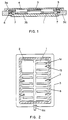
- Figure 1 is a sectional view showing an assembly structure of a pressure contact type semiconductor device according to an embodiment of the present invention.
- Figure 2 is a plan view showing an arrangement of parts incorporated in a flat package in Figure 1.
- Figures 3a and 3b show the structure of a contact terminal body in Figure 1; Figure 3a is a bottom view and Figure 3b is a side view.
- Figures 4a and 4b show a bonded wafer employed in IGBTs in Figure 1; Figure 4a shows a state before bonding and Figure 4b shows a state after the bonding.
- Figures 5a and 5b show a bonded wafer employed in a flywheel diode in Figure 1; Figure 5a shows a state before bonding and Figure 5b shows a state after the bonding.
- Figures 1 and 2 show a pressure contact type IGBT module in which five IGBTs and one flywheel diode are placed adjacent to each other in a substantially coplanar array within a flat package.
- an array of six chips is arranged in two rows of three, one row comprising three IGBTs 1, and the other row comprising two IGBTs 1 and a flywheel diode 2.
- a pressure contact type flat package 3 encloses the IGBTs 1 and the flywheel diode 2.
- a silicon substrate of each IGBT 1 has a size of about 20 mm x 20 mm.
- the bottom principal face of the IGBT 1 (the underside as seen in Figure 1) is made the collector, and two strip-like emitter electrodes 1a each having a width of about 2 mm and a length of about 16 mm are formed on the upper principal face (as seen in Figure 1) so as to avoid a gate structure with a gate electrode 1b formed between the emitter electrodes 1a.
- the flywheel diode 2 is placed adjacent to the IGBTs 1 in the flat package 3 such that the top face and the bottom face of the silicon substrate are made the anode and cathode, respectively.
- the silicon substrates of the IGBT 1 and the flywheel diode 2 are produced from bonding wafer types so that the total thicknesses of those substrates are equalized. More specifically, as shown in Figures 4a and 4b, the silicon substrate of the IGBT 1 is formed such that an n - wafer le having an epitaxially grown n + layer 1d is bonded to a p + wafer (highly doped silicon substrate) 1c as a base. The total thickness of the substrate is t. On the other hand, as shown in Figures 5a and 5b.
- the silicon substrate of the flywheel diode 2 is formed such that an n - wafer 2c having an epitaxially grown n + layer 2b is bonded to an n + wafer (highly doped silicon substrate) 2a.
- the thickness of the n + wafer 2a is adjusted so that the total thickness becomes equal to that of the silicon substrate of the IGBT 1, i.e., t.
- the aforementioned flat package 3 consists of a pair of common electrode plates 3a and 3b respectively exposed to the top and bottom face sides and opposed to the emitters and collectors of the IGBTs 1, and a ceramic insulating outer frame 3c interposed between the peripheries of the common electrode plates 3a and 3b so as sealingly to join the edge regions of those plates. That is, a hermetically sealed package is constituted of the above parts.
- a respective contact terminal body 4 serving both as a heat radiator and as a pressure member, is interposed between the emitter electrodes 1a of each IGBT 1 and the top-face-side main electrode of the flywheel electrode 2 and common electrode plate 3a forming the upper face of the package 3.
- the contact terminal body 4 is a rectangular plate made of a material, such as molybdenum, having superior thermal and electrical conductivity. While its top face 4c is finished into a flat surface to contact the electrode plate 3a, the opposite face, intended to contact the IGBT 1, has two protruding strips 4a that are to make area contact with the emitter electrodes 1a of the IGBT 1. Further, recessed cutouts 4b are formed in peripheral portions of the contact terminal body 4 to avoid contact with a wire leading from a gate electrode 1b of the IGBT 1, which will be described later.
- the external dimensions of the contact terminal bodies 4 are determined in accordance with the chip sizes of the IGBTs 1 and the flywheel diode 2, and their thicknesses are the same.
- the contact terminal bodies 4 are held in place in the package by use of an interposing positioning plate 5 made of heat-resisting resin or rubber.
- the positioning plate 5 is fitted in the flat package 3 such that its periphery contacts with the inner wall of the insulating outer frame 3c of the package 3, and has windows at positions corresponding to the positions of the IGBTs 1 and the flywheel diode 2 so that the contact terminal bodies 4 can be fitted in the windows.
- tongues to engage with the cutouts 4b (see Figure 3) be formed so as to project into each window, to ensure the correct rotational positioning of the terminal bodies 4.
- a gate wiring conductor 6 (hatched in the Figures) is evaporated onto the top face of a step (wiring base) that is formed in the inner wall of the insulating outer frame 3c of the flat package 3, to extend over the entire circumference of the frame 3c.
- the gate electrodes 1b of the respective IGBTs 1 are connected to the gate wiring conductor 6 by gate wire leads 7 bonded thereto.
- the gate wire leads 7 do not contact the contact terminal bodies 4 because the gate wire leads 7 are led out through the cutouts 4b of the terminal bodies 4 (see Figure 3).
- the gate wiring conductor 6 is connected to a gate external lead terminal 6a that penetrates through the insulating outer frame 3c to be led outside the package 3.
- the invention provides the following advantages that a plurality of semiconductor chips can be incorporated in the flat package without exerting undue pressure on the control electrode structures of the semiconductor chips, to provide uniform pressure contact by plane contact.
- Heat dissipation to the exterior can be effected through the electrodes formed on both of the first and second principal surfaces of each semiconductor chip.
- the heat dissipation performance can be greatly improved to thereby much increase the current capacity of the semiconductor device. Since no bonding wires are used for the connection to the main electrodes, the internal wiring inductance is reduced, which, combined with the flat package of the hermetic seal structure, improves the reliability of the semiconductor device.
Landscapes
- Die Bonding (AREA)
- Cooling Or The Like Of Semiconductors Or Solid State Devices (AREA)
Claims (4)
- Halbleiterbauelement mit Druckkontakt, bei dem mehrere Chips (1) mit Bipolartransistoren mit isolierten Gateelektroden (IGBT) und mit jeweils einer ersten Hauptelektrode (1a) und einer Steuerelektrode (1b) auf einer ersten Hauptfläche und mit einer zweiten Hauptelektrode auf einer zweiten Hauptfläche in einem Flachgehäuse (3) so untergebracht sind, daß sie nebeneinanderliegen, und das Halbleiterbauelement des weiteren zumindest einen Flywheel-Dioden-Chip (2) mit einer ersten Hauptelektrode auf einer ersten Hauptfläche und einer zweiten Hauptelektrode auf einer zweiten Hauptfläche enthält, wobei der Flywheel-Dioden-Chip (2) und die IGBT-Chips (1) eine gebondete Wafer-Bauweise besitzen, die dadurch entsteht, daß ein hochdotiertes Siliciumsubstrat so auf die Seite der zweiten Hauptfläche gebondet ist, daß der Dioden-Chip und die IGBT-Chips (1, 2) die gleiche Höhe aufweisen, und im selben Flachgehäuse (3) so untergebracht sind, daß der Dioden-Chip (2) neben den IGBT-Chips (1) angeordnet ist, wobei das Flachgehäuse einen äußeren Isolierrahmen (3c), der zwischen den gegenüberliegenden Seiten zweier Platten der gemeinsamen Elektroden (3a, 3b) angeordnet und bei gleichzeitiger Abdichtung damit verbunden ist, und als Druckelemente und Wärmestrahler dienende Kontaktanschlußkörper (4) zwischen den ersten Hauptelektroden (1a) des entsprechenden Dioden-Chips und der entsprechenden IGBT-Chips (1, 2) und der gegenüberliegenden Platte der gemeinsamen Elektrode (3a) des Gehäuses umfaßt, wobei die Steuerelektroden (1b) der entsprechenden IGBT-Chips (1) über einen Draht mit einer am inneren Umfang des Gehäuses vorgesehenen Steuerelektrodenvedrahtungsleiterbahn (6) verbunden sind, und ein äußerer Zuleitungsanschluß (6a) für die Steuerelektroden von der Außenseite durch das Gehäuse an die Verdrahtungsleiterbahn geführt ist, dadurch gekennzeichnet, daß ein Positionierungselement (5) zum Festhalten der mit den ersten Hauptelektroden (1a) des entsprechenden Dioden-Chips und der entsprechenden IGBT-Chips (1, 2) in Kontakt stehenden Kontaktanschlußkörper (4) in dem Flachgehäuse angeordnet ist und wobei zumindest eine Aussparung (4b) am Umfang jedes Kontaktanschlußkörpers (4) vorhanden ist, um eine Berührung mit einem von der Steuerelektrode (1b) des IGBT-Chips (1) kommenden Verbindungsdraht (7) zu vermeiden, und wobei der Umfang des Positionierungselements (5) mit der Innenwand des äußeren Isolierrahmens (3c) des Gehäuses (3) in Kontakt steht und das Positionierungselement (5) an den dem Dioden-Chip und den IGBT-Chips (1, 2) entsprechenden Positionen Fenster besitzt, und wobei die Kontaktanschlußkörper (4) in die Fenster passen.
- Halbleiterbauelement mit Druckkontakt nach Anspruch 1, dadurch gekennzeichnet, daß die Steuerelektrodenverdrahtungsleiterbahn (6) an der Innenwand des äußeren Isolierrahmens (3c) des Flachgehäuses (3) so geformt ist, daß sie den Dioden-Chip und die IGBT-Chips (1) umgibt, und der an einem Ende mit der Steuerelektrodenverdrahtungsleiterbahn (6) verbundene äußere Zuleitungsanschluß (6a) durch den äußeren Isolierrahmen (3c) aus dem Gehäuse (3) herausführt.
- Halbleiterbauelement mit Druckkontakt nach Anspruch 1, dadurch gekennzeichnet, daß die Oberseiten (4c) der Kontaktanschlußkörper (4) ebene, mit der Elektrodenplatte (3a) in Kontakt stehende Flächen sind, während die gegenüberliegenden Seiten der mit den entsprechenden IGBT-Chips (1) in Kontakt stehenden Kontaktanschlußkörper (4) zwei vorstehende Streifen (4a) besitzt, so daß ein Flächenkontakt mit den Emitterelektroden (1a) der IGBT-Chips (1) entsteht.
- Halbleiterbauelement mit Druckkontakt nach einem der Ansprüche 1 bis 3, dadurch gekennzeichnet, daß die zweiten Hauptflächen des entsprechenden Dioden-Chips und der entsprechenden IGBT-Chips (1, 2) und die gegenüberliegende Elektrodenplatte (3b) über dazwischen angeordnete leiffähige Thermoplastfolien, wie beispielsweise Lötfolien, miteinander gebondet sind.
Priority Applications (1)
| Application Number | Priority Date | Filing Date | Title |
|---|---|---|---|
| EP19970104435 EP0784342B1 (de) | 1993-07-27 | 1994-07-25 | Halbleiterbauelement mit Druckkontakt und dessen Montage |
Applications Claiming Priority (4)
| Application Number | Priority Date | Filing Date | Title |
|---|---|---|---|
| JP18427193 | 1993-07-27 | ||
| JP184271/93 | 1993-07-27 | ||
| JP02862394A JP3180863B2 (ja) | 1993-07-27 | 1994-02-28 | 加圧接触形半導体装置およびその組立方法 |
| JP28623/94 | 1994-02-28 |
Related Child Applications (1)
| Application Number | Title | Priority Date | Filing Date |
|---|---|---|---|
| EP19970104435 Division EP0784342B1 (de) | 1993-07-27 | 1994-07-25 | Halbleiterbauelement mit Druckkontakt und dessen Montage |
Publications (2)
| Publication Number | Publication Date |
|---|---|
| EP0637080A1 EP0637080A1 (de) | 1995-02-01 |
| EP0637080B1 true EP0637080B1 (de) | 1998-09-09 |
Family
ID=26366761
Family Applications (2)
| Application Number | Title | Priority Date | Filing Date |
|---|---|---|---|
| EP19940305463 Expired - Lifetime EP0637080B1 (de) | 1993-07-27 | 1994-07-25 | Halbleiterbauelement mit Druckkontakt |
| EP19970104435 Expired - Lifetime EP0784342B1 (de) | 1993-07-27 | 1994-07-25 | Halbleiterbauelement mit Druckkontakt und dessen Montage |
Family Applications After (1)
| Application Number | Title | Priority Date | Filing Date |
|---|---|---|---|
| EP19970104435 Expired - Lifetime EP0784342B1 (de) | 1993-07-27 | 1994-07-25 | Halbleiterbauelement mit Druckkontakt und dessen Montage |
Country Status (4)
| Country | Link |
|---|---|
| US (2) | US5539220A (de) |
| EP (2) | EP0637080B1 (de) |
| JP (1) | JP3180863B2 (de) |
| DE (2) | DE69413160T2 (de) |
Cited By (1)
| Publication number | Priority date | Publication date | Assignee | Title |
|---|---|---|---|---|
| CN101958377A (zh) * | 2009-06-08 | 2011-01-26 | Lg伊诺特有限公司 | 发光器件、发光器件封装和具有该发光器件的照明系统 |
Families Citing this family (41)
| Publication number | Priority date | Publication date | Assignee | Title |
|---|---|---|---|---|
| JP3258200B2 (ja) * | 1995-05-31 | 2002-02-18 | 株式会社東芝 | 圧接型半導体装置 |
| JP3256636B2 (ja) * | 1994-09-15 | 2002-02-12 | 株式会社東芝 | 圧接型半導体装置 |
| FR2736206B1 (fr) * | 1995-06-30 | 1997-08-08 | Commissariat Energie Atomique | Procede de realisation d'un substrat d'interconnexion permettant de connecter une puce sur un substrat de reception |
| JPH09135023A (ja) * | 1995-11-08 | 1997-05-20 | Toshiba Corp | 圧接型半導体装置 |
| JP3018971B2 (ja) * | 1995-12-18 | 2000-03-13 | 富士電機株式会社 | 半導体装置 |
| US5661315A (en) * | 1995-12-28 | 1997-08-26 | Asea Brown Boveri Ag | Controllable power semiconductor component |
| US5998227A (en) * | 1996-02-01 | 1999-12-07 | International Rectifier Corporation | IGBT and free-wheeling diode combination |
| DE19644009A1 (de) * | 1996-10-31 | 1998-05-07 | Siemens Ag | Großflächiges Hochstrommodul eines feldgesteuerten, abschaltbaren Leistungs-Halbleiterschalters |
| DE19726534A1 (de) * | 1997-06-23 | 1998-12-24 | Asea Brown Boveri | Leistungshalbleitermodul mit geschlossenen Submodulen |
| DE19732738A1 (de) * | 1997-07-30 | 1999-02-04 | Asea Brown Boveri | Leistungshalbleiterbauelemente mit druckausgleichender Kontaktplatte |
| JP3344552B2 (ja) | 1997-09-17 | 2002-11-11 | 株式会社東芝 | 圧接型半導体装置 |
| JP2930074B1 (ja) * | 1998-06-02 | 1999-08-03 | 富士電機株式会社 | 半導体装置 |
| FR2785447B1 (fr) * | 1998-10-30 | 2000-12-15 | Alstom Technology | Procede de raccordement electrique de puces de transistor igbt montees sur une plaquette de circuits integres |
| EP1168446A3 (de) | 2000-06-23 | 2008-01-23 | Westcode Semiconductors Limited | Gehäuse von Halbleiterchips |
| GB0015484D0 (en) * | 2000-06-23 | 2000-08-16 | Westcode Semiconductors Limite | Housing semiconductor chips |
| DE10102750B4 (de) * | 2001-01-22 | 2006-04-20 | Siemens Ag | Schaltungsanordnung |
| US6677669B2 (en) * | 2002-01-18 | 2004-01-13 | International Rectifier Corporation | Semiconductor package including two semiconductor die disposed within a common clip |
| JP2003258178A (ja) * | 2002-02-27 | 2003-09-12 | Sanyo Electric Co Ltd | 半導体装置 |
| JP2003258179A (ja) * | 2002-02-28 | 2003-09-12 | Sanyo Electric Co Ltd | 半導体装置およびその製造方法 |
| US6678163B1 (en) | 2002-12-19 | 2004-01-13 | Westcode Semiconductors Limited | Housing for semiconductor chips |
| US6991961B2 (en) * | 2003-06-18 | 2006-01-31 | Medtronic, Inc. | Method of forming a high-voltage/high-power die package |
| DE102004018476B4 (de) * | 2004-04-16 | 2009-06-18 | Infineon Technologies Ag | Leistungshalbleiteranordnung mit kontaktierender Folie und Anpressvorrichtung |
| JP4095049B2 (ja) * | 2004-08-30 | 2008-06-04 | シャープ株式会社 | 電極気密封止を用いた高信頼性半導体装置 |
| JP4453498B2 (ja) * | 2004-09-22 | 2010-04-21 | 富士電機システムズ株式会社 | パワー半導体モジュールおよびその製造方法 |
| ATE535018T1 (de) * | 2004-12-17 | 2011-12-15 | Siemens Ag | Halbleiterschaltmodul |
| JP4498170B2 (ja) * | 2005-03-02 | 2010-07-07 | 三菱電機株式会社 | 半導体装置及びその製造方法 |
| JP4478049B2 (ja) * | 2005-03-15 | 2010-06-09 | 三菱電機株式会社 | 半導体装置 |
| DE102005050534B4 (de) * | 2005-10-21 | 2008-08-07 | Semikron Elektronik Gmbh & Co. Kg | Leistungshalbleitermodul |
| DE102007054709B4 (de) | 2007-11-16 | 2014-11-13 | Semikron Elektronik Gmbh & Co. Kg | Leistungshalbleitermodul mit einem Substrat und mit einer Druckeinrichtung |
| EP2071621A1 (de) * | 2007-12-11 | 2009-06-17 | ABB Research Ltd. | Halbleiterschaltungsanordnung mit Gate-Anschluß |
| EP2088623A1 (de) * | 2008-02-07 | 2009-08-12 | ABB Oy | Elektrisches Modul mit mehreren elektrischen Bauelementen |
| JP5709299B2 (ja) | 2010-09-29 | 2015-04-30 | ローム株式会社 | 半導体パワーモジュールおよびその製造方法 |
| US8637981B2 (en) * | 2011-03-30 | 2014-01-28 | International Rectifier Corporation | Dual compartment semiconductor package with temperature sensor |
| CN103681547A (zh) * | 2012-09-21 | 2014-03-26 | 北京新创椿树整流器件有限公司 | 平板封装压接式引出电极绝缘栅双极型晶体管元件 |
| JP2014135527A (ja) * | 2014-04-30 | 2014-07-24 | Rohm Co Ltd | 半導体パワーモジュールおよびその製造方法 |
| WO2016062426A1 (en) | 2014-10-24 | 2016-04-28 | Abb Technology Ag | Semiconductor module and stack arrangement of semiconductor modules |
| KR101686745B1 (ko) | 2015-08-07 | 2016-12-15 | 재단법인 다차원 스마트 아이티 융합시스템 연구단 | 파워 앰프 모듈 패키지 및 그 패키징 방법 |
| KR102348252B1 (ko) * | 2015-08-07 | 2022-01-07 | 주식회사 워프솔루션 | 파워 앰프 모듈 패키지 및 그 패키징 방법 |
| EP3462479B1 (de) * | 2017-10-02 | 2020-12-09 | General Electric Technology GmbH | Halbleiteranordnung mit fehlerschutz |
| CN115561601A (zh) * | 2021-07-01 | 2023-01-03 | 全球能源互联网研究院有限公司 | 一种压接型igbt子模组测试适配器及测试设备 |
| FR3154540B1 (fr) * | 2023-10-18 | 2025-10-24 | Commissariat A L’Energie Atomique Et Aux Energies Alternatives | Module de puissance et procédé de fabrication |
Family Cites Families (17)
| Publication number | Priority date | Publication date | Assignee | Title |
|---|---|---|---|---|
| DE2838997A1 (de) * | 1978-09-07 | 1980-03-20 | Bbc Brown Boveri & Cie | Verfahren zur herstellung eines dichten gehaeuses fuer einen scheibenfoermigen, mindestens einen pn-uebergang aufweisenden halbleiterkoerper |
| US4313128A (en) * | 1979-05-08 | 1982-01-26 | Westinghouse Electric Corp. | Compression bonded electronic device comprising a plurality of discrete semiconductor devices |
| JPH081914B2 (ja) * | 1987-03-31 | 1996-01-10 | 株式会社東芝 | 圧接型半導体装置 |
| JPH0628292B2 (ja) * | 1988-11-11 | 1994-04-13 | 富士電機株式会社 | 逆阻止形トランジスタモジュール |
| US5001542A (en) * | 1988-12-05 | 1991-03-19 | Hitachi Chemical Company | Composition for circuit connection, method for connection using the same, and connected structure of semiconductor chips |
| DE69009259T2 (de) * | 1989-02-02 | 1994-10-13 | Matsushita Electric Ind Co Ltd | Verfahren zum Zusammensetzen von Halbleiteranordnungen. |
| US4999077A (en) * | 1989-08-31 | 1991-03-12 | Xerox Corporation | Method of fabricating full width scanning or imaging arrays from subunits |
| JPH0744264B2 (ja) * | 1989-10-31 | 1995-05-15 | 株式会社東芝 | 圧接型半導体装置 |
| US5045142A (en) * | 1989-11-22 | 1991-09-03 | Xerox Corporation | Stand-off structure for flipped chip butting |
| JPH0744191B2 (ja) * | 1989-12-15 | 1995-05-15 | 三菱電機株式会社 | 半導体装置およびそのための電極ブロック |
| JP2755761B2 (ja) * | 1990-01-26 | 1998-05-25 | 株式会社東芝 | 半導体装置 |
| JP3137375B2 (ja) * | 1990-09-20 | 2001-02-19 | 株式会社東芝 | 圧接型半導体装置 |
| JPH04160708A (ja) * | 1990-10-22 | 1992-06-04 | Nec Corp | 電極端子の接続方法 |
| DE59107655D1 (de) * | 1991-02-22 | 1996-05-09 | Asea Brown Boveri | Abschaltbares Hochleistungs-Halbleiterbauelement |
| US5149662A (en) * | 1991-03-27 | 1992-09-22 | Integrated System Assemblies Corporation | Methods for testing and burn-in of integrated circuit chips |
| DE69109468T2 (de) * | 1991-05-23 | 1995-12-14 | Ansaldo Trasporti Spa | Elektronische Leistungsanordnung realisiert durch eine Reihe elementarer Halbleiterbauelemente in Parallelverbindung und verwandtes Herstellungsverfahren. |
| US5352629A (en) * | 1993-01-19 | 1994-10-04 | General Electric Company | Process for self-alignment and planarization of semiconductor chips attached by solder die adhesive to multi-chip modules |
-
1994
- 1994-02-28 JP JP02862394A patent/JP3180863B2/ja not_active Expired - Fee Related
- 1994-07-25 DE DE69413160T patent/DE69413160T2/de not_active Expired - Fee Related
- 1994-07-25 DE DE69421831T patent/DE69421831T2/de not_active Expired - Fee Related
- 1994-07-25 EP EP19940305463 patent/EP0637080B1/de not_active Expired - Lifetime
- 1994-07-25 EP EP19970104435 patent/EP0784342B1/de not_active Expired - Lifetime
- 1994-07-26 US US08/280,618 patent/US5539220A/en not_active Expired - Lifetime
-
1995
- 1995-04-25 US US08/428,914 patent/US5635427A/en not_active Expired - Lifetime
Cited By (2)
| Publication number | Priority date | Publication date | Assignee | Title |
|---|---|---|---|---|
| CN101958377A (zh) * | 2009-06-08 | 2011-01-26 | Lg伊诺特有限公司 | 发光器件、发光器件封装和具有该发光器件的照明系统 |
| CN101958377B (zh) * | 2009-06-08 | 2013-03-20 | Lg伊诺特有限公司 | 发光器件、发光器件封装和具有该发光器件的照明系统 |
Also Published As
| Publication number | Publication date |
|---|---|
| US5635427A (en) | 1997-06-03 |
| DE69421831D1 (de) | 1999-12-30 |
| DE69413160D1 (de) | 1998-10-15 |
| JPH0794673A (ja) | 1995-04-07 |
| DE69413160T2 (de) | 1999-02-18 |
| JP3180863B2 (ja) | 2001-06-25 |
| EP0637080A1 (de) | 1995-02-01 |
| DE69421831T2 (de) | 2000-03-09 |
| EP0784342B1 (de) | 1999-11-24 |
| EP0784342A3 (de) | 1997-08-20 |
| EP0784342A2 (de) | 1997-07-16 |
| US5539220A (en) | 1996-07-23 |
Similar Documents
| Publication | Publication Date | Title |
|---|---|---|
| EP0637080A1 (de) | Halbleiterbauelement mit Druckkontakt und dessen Montageverfahren | |
| JP3256636B2 (ja) | 圧接型半導体装置 | |
| US7569920B2 (en) | Electronic component having at least one vertical semiconductor power transistor | |
| JP3847676B2 (ja) | パワー半導体装置 | |
| EP0962973B1 (de) | Mehrchip-Halbleiter-Leistungsbauelement vom Druckkontakttyp | |
| KR20230092516A (ko) | 양면 방열 전력반도체모듈 및 그 제조방법 | |
| JP3129020B2 (ja) | 半導体装置 | |
| US12489031B2 (en) | Semiconductor device and manufacturing method thereof | |
| US11201099B2 (en) | Semiconductor device and method of manufacturing the same | |
| EP1231635A1 (de) | Herstellungsverfahren eines elektronischen Leistungsbauteils und einer Diode in der gleichen Packung | |
| US20200266130A1 (en) | Semiconductor device | |
| JP2002151646A (ja) | 圧接型半導体装置 | |
| US20230197581A1 (en) | Power semiconductor module and method of manufacturing the same | |
| JP3644161B2 (ja) | パワー半導体モジュール | |
| US6081039A (en) | Pressure assembled motor cube | |
| US5798287A (en) | Method for forming a power MOS device chip | |
| JP3264190B2 (ja) | 半導体装置 | |
| EP4738436A1 (de) | Leistungsmodul | |
| JP3166527B2 (ja) | 加圧接触形半導体装置 | |
| JP3995618B2 (ja) | 半導体装置 | |
| JP3180868B2 (ja) | 加圧接触形半導体装置の製造方法 | |
| WO1987001866A1 (en) | Semiconductor device | |
| CN117810267A (zh) | 一种栅极嵌埋式mosfet器件及其制造方法 | |
| JPH09275186A (ja) | 半導体装置 | |
| JPH10270475A (ja) | 圧接型半導体装置 |
Legal Events
| Date | Code | Title | Description |
|---|---|---|---|
| PUAI | Public reference made under article 153(3) epc to a published international application that has entered the european phase |
Free format text: ORIGINAL CODE: 0009012 |
|
| AK | Designated contracting states |
Kind code of ref document: A1 Designated state(s): CH DE GB LI |
|
| 17P | Request for examination filed |
Effective date: 19950329 |
|
| 17Q | First examination report despatched |
Effective date: 19950919 |
|
| GRAG | Despatch of communication of intention to grant |
Free format text: ORIGINAL CODE: EPIDOS AGRA |
|
| GRAG | Despatch of communication of intention to grant |
Free format text: ORIGINAL CODE: EPIDOS AGRA |
|
| GRAH | Despatch of communication of intention to grant a patent |
Free format text: ORIGINAL CODE: EPIDOS IGRA |
|
| GRAH | Despatch of communication of intention to grant a patent |
Free format text: ORIGINAL CODE: EPIDOS IGRA |
|
| GRAA | (expected) grant |
Free format text: ORIGINAL CODE: 0009210 |
|
| DX | Miscellaneous (deleted) | ||
| AK | Designated contracting states |
Kind code of ref document: B1 Designated state(s): CH DE GB LI |
|
| REG | Reference to a national code |
Ref country code: CH Ref legal event code: NV Representative=s name: JACOBACCI & PERANI S.A. Ref country code: CH Ref legal event code: EP |
|
| REF | Corresponds to: |
Ref document number: 69413160 Country of ref document: DE Date of ref document: 19981015 |
|
| PLBE | No opposition filed within time limit |
Free format text: ORIGINAL CODE: 0009261 |
|
| STAA | Information on the status of an ep patent application or granted ep patent |
Free format text: STATUS: NO OPPOSITION FILED WITHIN TIME LIMIT |
|
| 26N | No opposition filed | ||
| PGFP | Annual fee paid to national office [announced via postgrant information from national office to epo] |
Ref country code: DE Payment date: 20010716 Year of fee payment: 8 |
|
| PGFP | Annual fee paid to national office [announced via postgrant information from national office to epo] |
Ref country code: GB Payment date: 20010725 Year of fee payment: 8 |
|
| PGFP | Annual fee paid to national office [announced via postgrant information from national office to epo] |
Ref country code: CH Payment date: 20010730 Year of fee payment: 8 |
|
| REG | Reference to a national code |
Ref country code: GB Ref legal event code: IF02 |
|
| PG25 | Lapsed in a contracting state [announced via postgrant information from national office to epo] |
Ref country code: GB Free format text: LAPSE BECAUSE OF NON-PAYMENT OF DUE FEES Effective date: 20020725 |
|
| PG25 | Lapsed in a contracting state [announced via postgrant information from national office to epo] |
Ref country code: LI Free format text: LAPSE BECAUSE OF NON-PAYMENT OF DUE FEES Effective date: 20020731 Ref country code: CH Free format text: LAPSE BECAUSE OF NON-PAYMENT OF DUE FEES Effective date: 20020731 |
|
| PG25 | Lapsed in a contracting state [announced via postgrant information from national office to epo] |
Ref country code: DE Free format text: LAPSE BECAUSE OF NON-PAYMENT OF DUE FEES Effective date: 20030201 |
|
| REG | Reference to a national code |
Ref country code: CH Ref legal event code: PL |
|
| GBPC | Gb: european patent ceased through non-payment of renewal fee |
Effective date: 20020725 |