EP0579291B1 - Housing structure for image forming apparatus - Google Patents
Housing structure for image forming apparatus Download PDFInfo
- Publication number
- EP0579291B1 EP0579291B1 EP93116306A EP93116306A EP0579291B1 EP 0579291 B1 EP0579291 B1 EP 0579291B1 EP 93116306 A EP93116306 A EP 93116306A EP 93116306 A EP93116306 A EP 93116306A EP 0579291 B1 EP0579291 B1 EP 0579291B1
- Authority
- EP
- European Patent Office
- Prior art keywords
- optical system
- housing
- image forming
- system housing
- walls
- Prior art date
- Legal status (The legal status is an assumption and is not a legal conclusion. Google has not performed a legal analysis and makes no representation as to the accuracy of the status listed.)
- Expired - Lifetime
Links
Images


Classifications
-
- G—PHYSICS
- G03—PHOTOGRAPHY; CINEMATOGRAPHY; ANALOGOUS TECHNIQUES USING WAVES OTHER THAN OPTICAL WAVES; ELECTROGRAPHY; HOLOGRAPHY
- G03G—ELECTROGRAPHY; ELECTROPHOTOGRAPHY; MAGNETOGRAPHY
- G03G15/00—Apparatus for electrographic processes using a charge pattern
-
- G—PHYSICS
- G03—PHOTOGRAPHY; CINEMATOGRAPHY; ANALOGOUS TECHNIQUES USING WAVES OTHER THAN OPTICAL WAVES; ELECTROGRAPHY; HOLOGRAPHY
- G03B—APPARATUS OR ARRANGEMENTS FOR TAKING PHOTOGRAPHS OR FOR PROJECTING OR VIEWING THEM; APPARATUS OR ARRANGEMENTS EMPLOYING ANALOGOUS TECHNIQUES USING WAVES OTHER THAN OPTICAL WAVES; ACCESSORIES THEREFOR
- G03B27/00—Photographic printing apparatus
- G03B27/32—Projection printing apparatus, e.g. enlarger, copying camera
- G03B27/52—Details
- G03B27/522—Projection optics
- G03B27/525—Projection optics for slit exposure
- G03B27/526—Projection optics for slit exposure in which the projection optics move
-
- G—PHYSICS
- G03—PHOTOGRAPHY; CINEMATOGRAPHY; ANALOGOUS TECHNIQUES USING WAVES OTHER THAN OPTICAL WAVES; ELECTROGRAPHY; HOLOGRAPHY
- G03B—APPARATUS OR ARRANGEMENTS FOR TAKING PHOTOGRAPHS OR FOR PROJECTING OR VIEWING THEM; APPARATUS OR ARRANGEMENTS EMPLOYING ANALOGOUS TECHNIQUES USING WAVES OTHER THAN OPTICAL WAVES; ACCESSORIES THEREFOR
- G03B27/00—Photographic printing apparatus
- G03B27/32—Projection printing apparatus, e.g. enlarger, copying camera
- G03B27/52—Details
- G03B27/54—Lamp housings; Illuminating means
- G03B27/542—Lamp housings; Illuminating means for copying cameras, reflex exposure lighting
-
- G—PHYSICS
- G03—PHOTOGRAPHY; CINEMATOGRAPHY; ANALOGOUS TECHNIQUES USING WAVES OTHER THAN OPTICAL WAVES; ELECTROGRAPHY; HOLOGRAPHY
- G03G—ELECTROGRAPHY; ELECTROPHOTOGRAPHY; MAGNETOGRAPHY
- G03G15/00—Apparatus for electrographic processes using a charge pattern
- G03G15/04—Apparatus for electrographic processes using a charge pattern for exposing, i.e. imagewise exposure by optically projecting the original image on a photoconductive recording material
-
- G—PHYSICS
- G03—PHOTOGRAPHY; CINEMATOGRAPHY; ANALOGOUS TECHNIQUES USING WAVES OTHER THAN OPTICAL WAVES; ELECTROGRAPHY; HOLOGRAPHY
- G03G—ELECTROGRAPHY; ELECTROPHOTOGRAPHY; MAGNETOGRAPHY
- G03G21/00—Arrangements not provided for by groups G03G13/00 - G03G19/00, e.g. cleaning, elimination of residual charge
- G03G21/16—Mechanical means for facilitating the maintenance of the apparatus, e.g. modular arrangements
- G03G21/1604—Arrangement or disposition of the entire apparatus
- G03G21/1619—Frame structures
-
- G—PHYSICS
- G03—PHOTOGRAPHY; CINEMATOGRAPHY; ANALOGOUS TECHNIQUES USING WAVES OTHER THAN OPTICAL WAVES; ELECTROGRAPHY; HOLOGRAPHY
- G03G—ELECTROGRAPHY; ELECTROPHOTOGRAPHY; MAGNETOGRAPHY
- G03G21/00—Arrangements not provided for by groups G03G13/00 - G03G19/00, e.g. cleaning, elimination of residual charge
- G03G21/16—Mechanical means for facilitating the maintenance of the apparatus, e.g. modular arrangements
- G03G21/1661—Mechanical means for facilitating the maintenance of the apparatus, e.g. modular arrangements means for handling parts of the apparatus in the apparatus
- G03G21/1666—Mechanical means for facilitating the maintenance of the apparatus, e.g. modular arrangements means for handling parts of the apparatus in the apparatus for the exposure unit
-
- G—PHYSICS
- G03—PHOTOGRAPHY; CINEMATOGRAPHY; ANALOGOUS TECHNIQUES USING WAVES OTHER THAN OPTICAL WAVES; ELECTROGRAPHY; HOLOGRAPHY
- G03G—ELECTROGRAPHY; ELECTROPHOTOGRAPHY; MAGNETOGRAPHY
- G03G21/00—Arrangements not provided for by groups G03G13/00 - G03G19/00, e.g. cleaning, elimination of residual charge
- G03G21/20—Humidity or temperature control also ozone evacuation; Internal apparatus environment control
- G03G21/206—Conducting air through the machine, e.g. for cooling, filtering, removing gases like ozone
-
- G—PHYSICS
- G03—PHOTOGRAPHY; CINEMATOGRAPHY; ANALOGOUS TECHNIQUES USING WAVES OTHER THAN OPTICAL WAVES; ELECTROGRAPHY; HOLOGRAPHY
- G03G—ELECTROGRAPHY; ELECTROPHOTOGRAPHY; MAGNETOGRAPHY
- G03G15/00—Apparatus for electrographic processes using a charge pattern
- G03G15/04—Apparatus for electrographic processes using a charge pattern for exposing, i.e. imagewise exposure by optically projecting the original image on a photoconductive recording material
- G03G15/043—Apparatus for electrographic processes using a charge pattern for exposing, i.e. imagewise exposure by optically projecting the original image on a photoconductive recording material with means for controlling illumination or exposure
- G03G15/0435—Apparatus for electrographic processes using a charge pattern for exposing, i.e. imagewise exposure by optically projecting the original image on a photoconductive recording material with means for controlling illumination or exposure by introducing an optical element in the optical path, e.g. a filter
-
- G—PHYSICS
- G03—PHOTOGRAPHY; CINEMATOGRAPHY; ANALOGOUS TECHNIQUES USING WAVES OTHER THAN OPTICAL WAVES; ELECTROGRAPHY; HOLOGRAPHY
- G03G—ELECTROGRAPHY; ELECTROPHOTOGRAPHY; MAGNETOGRAPHY
- G03G2221/00—Processes not provided for by group G03G2215/00, e.g. cleaning or residual charge elimination
- G03G2221/16—Mechanical means for facilitating the maintenance of the apparatus, e.g. modular arrangements and complete machine concepts
- G03G2221/1636—Mechanical means for facilitating the maintenance of the apparatus, e.g. modular arrangements and complete machine concepts for the exposure unit
Definitions
- the present invention relates to a housing structure for use in an electrophotographic image forming apparatus such as a photocopying machine.
- Electrophotographic image forming apparatus such as photocopying machines, laser beam printers, or the like are widely used in offices and other applications.
- a housing structure which comprises a housing that contains an image forming mechanism including a photosensitive body and another housing that accommodates a scanning exposure optical system for optically scanning a subject and exposing the photosensitive body to an optical image of the subject.
- the housing which houses the scanning exposure optical system is placed on and fixed to the housing which houses the image forming mechanism.
- These housings are basically optically independent of, or isolated from, each other so that no light from a light source for applying scanning light to the subject in the exposure optical system will directly fall on the photosensitive body, thus preventing noise from being included in the final image.
- the independent housings can be installed and removed separately from each other.
- the housing which houses the scanning exposure optical system hereinafter referred to as the "optical system housing", including a glass platen for supporting the subject on its upper surface, tends to be heated to high temperature, making the user feel anxious about the condition of the scanning exposure optical system or sometimes making the user feel hot.
- external air is introduced into the optical system housing to cool the internal scanning exposure optical system and the glass platen so that they will not be unduly heated.
- the cooling air is forcibly delivered into the optical system housing by a fan.
- the optical system housing has an air inlet for introducing the cooling air and an air outlet for discharging the air after it has cooled the scanning exposure optical system and the glass platen.
- the air inlet is equipped with a filter for preventing dust from entering the optical system housing through the air inlet.
- the air outlet is usually left open without any filter.
- the various components are housed in the housings in accurate positions and with accurate attitudes. Unless the housings are coupled to each other in an accurate position and with an accurate attitude, however, the optical images cannot be formed on the photosensitive body by the scanning exposure optical system.
- FIG. 1 shows in vertical cross section an electrophotographic photocopying machine as an image forming apparatus which has an optical system housing structure according to the present invention.
- the photocopying machine comprises a scanning exposure optical system 1, an image forming mechanism 3 for producing an image through exposure by the scanning exposure optical system 1 and transferring the image to an image transfer sheet 2, and a sheet feed mechanism 4 for feeding an image transfer sheet 2 to the image forming mechanism 3.
- the scanning exposure optical system 1, the image forming mechanism 3, and the sheet feed mechanism 4 are housed respectively in an optical system housing 6, an image forming mechanism housing 7, and a sheet feed mechanism housing 8, which are independent of each other.
- the optical system housing 6 is placed on the image forming mechanism housing 7 which is positioned on the sheet feed mechanism housing 8. These housings 6, 7, 8 which are thus stacked is coupled together, thus providing a machine frame 9.
- the scanning exposure optical system 1 has a lamp 13 for applying scanning line to a subject (not shown) on a glass platen 11, the lamp 13 being supported on a first slider 12 movable below the glass platen 11. Light reflected from the subject on the glass platen 11 is reflected by a first mirror 14 supported on the first slider 13. A second slider 15 is also movable below the glass platen 11 and supports second and third mirrors 17, 18. Fourth and fifth mirrors 19, 20 are supported on a third slider 16 movably disposed below the glass platen 11. The second through fifth mirrors 17 through 20 serve to keep a constant optical path for the light reflected from the first mirror 14.
- the scanning exposure optical system 1 also has a projection lens 21 disposed between the third and fourth mirrors 18, 19. A sixth mirror 22 disposed near the fifth mirror 20 serves to correct the length of the optical axis when the magnification is varied by movement of the projection lens 21 along its optical axis.
- the image forming mechanism 3 comprises a photosensitive drum 31, a charging charger 32, an image developing unit 33, a transfer charger 32, a separation charger 135, and a cleaning unit 136, which are successively disposed around the photosensitive drum 31.
- the image forming mechanism 32 operates according to the known electrophotographic process, i.e., forms a toner image on the photosensitive drum 31 based on an electrostatic latent image formed thereon, and transfers the toner image onto a transfer sheet 2 supplied to the photosensitive drum 31.
- a sheet feed path 35 extends from the sheet feed mechanism 4 to an image transfer region where the photosensitive drum 31 and the transfer charger 34 confront each other.
- the sheet feed path 35 serves to supply a transfer sheet 2 from the sheet feed mechanism 4 to the image transfer region.
- the sheet feed path 35 has a pair of timing rollers 36. When the timing rollers 36 are at rest, a transfer sheet 2 is fed to the timing rollers 36, and has its leading edge aligned thereby so that the transfer sheet 2 is corrected out of any skewed condition. Then, the timing rollers 36 are rotated to feed the transfer sheet 2 to the image transfer region. Therefore, the timing to supply the transfer sheet 2 to the image transfer region can be adjusted by the timing rollers 36.
- the image forming mechanism 3 further includes a feed unit 37 comprising a feed belt for attracting and feeding the transfer sheet 2 onto which the toner image has been transferred.
- the toner image on the transfer sheet 2 is then fixed by a fixing unit 38.
- the transfer sheet 2 from the fixing unit 38 is discharged by discharge rollers 39.
- the sheet feed mechanism 4 comprises three sheet feeders 41, 42, 43 storing transfer sheets 2 of different sizes.
- the transfer sheets 2 of different sizes are selectively fed from the sheet feeders 41, 42, 43 to the image forming mechanism 3 through the sheet feed path 35.
- the sheet feeders 41, 42, 43 have respective sheet cassettes 44, 45, 46 for storing transfer sheets, respective pickup rollers 47, 48, 49 for delivering transfer sheets from within the sheet cassettes 44, 45, 46, and respective separator pads 50 for separating the transfer sheets from each other so that they will be fed one at a time.
- the sheet feeders 41, 42, 43 are unitized as blocks, which can be replaced with other blocks. For example, two sheet feeders may be replaced with one sheet feeder which stores a greater number of sheets.
- the sheet cassettes 41, 42, 43 may be loaded and unloaded through a front panel of the machine frame 9, i.e., in directions toward and away from the viewer of FIG. 1.
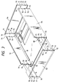
- the optical system housing 6 has air inlet holes 52 defined in a rear wall 51, and air outlet holes 55, 56 defined in lateral side walls 53, 54.
- An air blower fan 57 is mounted on the outside of the rear wall 51 over the air inlet holes 52, for introducing external air into the optical system housing 6 and discharging air from the optical system housing 6 through the air outlet holes 55, 56.
- air blower fan 57 When the air blower fan 57 is actuated, air flows as indicated by the arrows in FIG. 2, thus cooling the interior of the optical system housing 6. Therefore, even when the lamp 13 is heated, the glass platen 11 is prevented from being unduly heated, so that the operator will not feel anxious or hot.
- the air inlet holes 52 are positioned near the lamp 13 as it is in a home position before the scanning exposure optical system 1 starts to operate. Accordingly, the region in the optical system housing 6 where the lamp 13 is positioned more often and the temperature is higher, is effectively cooled by the cooling air introduced through the air inlet holes 52. Thus, the cooling efficiency of the scanning exposure optical system 1 is high.
- the machine frame 9 is covered with a resin cover 58 which has air ventilation holes 59 (FIG. 1) defined therein in registry with the air inlet and outlet holes 52, 55, 56 for allowing air to be introduced into and discharged out of the optical system housing 6.
- electrostatic filters 61, 62 are disposed at the air inlet and outlet holes 52, 55, 56 for trapping small dust particles under electrostatic attractive forces.
- the electrostatic filters 61, 62 may be of a known nature disclosed in Japanese Patent No. 1102749, and are manufactured by Sumitomo 3M Co., Ltd. and Toyobo Co., Ltd.
- the filter 61 is mounted over an air inlet port 162 of the air blower fan 57.
- the air blower fan 57 has guide slots 63 in which ends of the filter 62 are inserted.
- the filter 61 is fastened to the air blower fan 57 by screws 64.
- the filters 62 are disposed over the air outlet holes 55, 56 with positioning teeth engaging in corresponding slots in the side walls of the optical system housing 6, and are fastened to the sides walls 53, 54 by screws 65.
- the total opening area of the air outlet holes 55, 56 is much larger than the total opening area of the air inlet holes 52. Accordingly, air flows through the air inlet holes 52 at a speed much higher than the speed at which air flows through the air outlet holes 55, 56.
- the electrostatic filters 61, 62 are constructed to induce different pressure losses with respect to such different air flow speeds in order to allow the cooling air to well cool the interior of the optical system housing 6 and also to cause the electrostatic filters 61, 62 to well trap dust particles regardless of the difference between the air flow speeds.
- the electrostatic filters of Sumitomo 3M and Toyobo were satisfactory with respect to cooling and dust removal capabilities.
- the electrostatic filters of Sumitomo 3M were effective for use in both the air inlet port 162 and the air outlet holes 55, 56.
- the side walls 53, 54, the rear wall 51, and a front wall 64 of the optical system housing 6 are held well perpendicularly to each other, and also to the bottom panel 62, and the optical system housing 6 is placed on and fixed to the image forming mechanism housing 7 in an accurate position and with an accurate attitude.
- the walls 51, 53, 54, 64 are held perpendicularly to each other and also to the bottom panel 62 by the abutting engagement between the confronting ends of the walls 51, 53, 54, 64 because the abutting ends are high in dimensional and positional accuracy.
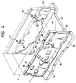
- the optical system housing 6 of the above structure is placed on and fixed to the image forming mechanism housing 7, as shown in FIG. 4.
- the image forming mechanism housing 7 comprises a bottom panel 81, drawn from a metal sheet, and a pair of front and rear confronting side walls 82, 83, each drawn from a metal sheet, mounted vertically on the bottom panel 81 in spaced relationship to each other.
- the side walls 82, 83 are fastened to the bottom panel 81 by bolts and nuts (not shown).
- the side walls 82, 83 have positioning surfaces 84 projecting downwardly and held against the bottom panel 81, so that the side walls 82, 83 can easily be positioned relatively to the bottom panel 81.
- the bottom panel 81 and the side walls 82, 83 are thus coupled to each other in accurate relative positional relationship.
- the front side wall 82 is taller than the rear side wall 83.
- the taller front side wall 82 has support fingers 85 pierced and raised with accuracy.
- the front side wall 82 also has an inner surface above the support fingers 85.
- One side of the optical system housing 6 is supported on the support fingers 85, and an outer surface of the supported side is held against the inner surface of the front side wall 82.
- the optical system housing 6 is therefore transversely positioned in a proper position and with a proper attitude easily by the inner surface of the front side wall 82.
- the rear side wall 83 has raised positioning surfaces 86 on its upper edge for supporting the opposite side of the optical system housing 6.
- the optical system housing 6 is easily placed on and fixed to the image forming mechanism housing 7 in a proper position and with a proper attitude, the first through fifth mirrors 14, 17 through 20 and the photosensitive drum 31 are maintained suitably parallel to each other and positioned appropriately relatively to each other.
- the high positional accuracy achieved between the components in the scanning exposure optical system 1 and the image forming mechanism 3 allows the image forming apparatus to produce images of high quality.
Landscapes
- Physics & Mathematics (AREA)
- General Physics & Mathematics (AREA)
- Optics & Photonics (AREA)
- Biodiversity & Conservation Biology (AREA)
- Engineering & Computer Science (AREA)
- Atmospheric Sciences (AREA)
- Life Sciences & Earth Sciences (AREA)
- Ecology (AREA)
- Environmental & Geological Engineering (AREA)
- Environmental Sciences (AREA)
- Mechanical Optical Scanning Systems (AREA)
- Exposure Or Original Feeding In Electrophotography (AREA)
- Electrophotography Configuration And Component (AREA)
Applications Claiming Priority (7)
| Application Number | Priority Date | Filing Date | Title |
|---|---|---|---|
| JP2103918A JPH043082A (ja) | 1990-04-19 | 1990-04-19 | 画像形成装置の光学系ボックス構造 |
| JP103918/90 | 1990-04-19 | ||
| JP2132240A JP2914517B2 (ja) | 1990-05-22 | 1990-05-22 | 走査光学機器の光学系ボックス |
| JP132241/90 | 1990-05-22 | ||
| JP132240/90 | 1990-05-22 | ||
| JP2132241A JP2992309B2 (ja) | 1990-05-22 | 1990-05-22 | 複写機のボックス構造 |
| EP91303540A EP0454381B1 (en) | 1990-04-19 | 1991-04-19 | Housing structure for image forming apparatus |
Related Parent Applications (1)
| Application Number | Title | Priority Date | Filing Date |
|---|---|---|---|
| EP91303540.8 Division | 1991-04-19 |
Publications (3)
| Publication Number | Publication Date |
|---|---|
| EP0579291A2 EP0579291A2 (en) | 1994-01-19 |
| EP0579291A3 EP0579291A3 (enExample) | 1994-04-13 |
| EP0579291B1 true EP0579291B1 (en) | 1996-02-14 |
Family
ID=27310105
Family Applications (3)
| Application Number | Title | Priority Date | Filing Date |
|---|---|---|---|
| EP93116306A Expired - Lifetime EP0579291B1 (en) | 1990-04-19 | 1991-04-19 | Housing structure for image forming apparatus |
| EP93116537A Expired - Lifetime EP0579292B1 (en) | 1990-04-19 | 1991-04-19 | Housing structure for image forming apparatus |
| EP91303540A Expired - Lifetime EP0454381B1 (en) | 1990-04-19 | 1991-04-19 | Housing structure for image forming apparatus |
Family Applications After (2)
| Application Number | Title | Priority Date | Filing Date |
|---|---|---|---|
| EP93116537A Expired - Lifetime EP0579292B1 (en) | 1990-04-19 | 1991-04-19 | Housing structure for image forming apparatus |
| EP91303540A Expired - Lifetime EP0454381B1 (en) | 1990-04-19 | 1991-04-19 | Housing structure for image forming apparatus |
Country Status (3)
| Country | Link |
|---|---|
| US (2) | US5243386A (enExample) |
| EP (3) | EP0579291B1 (enExample) |
| DE (3) | DE69116897T2 (enExample) |
Families Citing this family (5)
| Publication number | Priority date | Publication date | Assignee | Title |
|---|---|---|---|---|
| US5819137A (en) * | 1997-06-30 | 1998-10-06 | Eastman Kodak Company | Integrated environmental management for reproduction apparatus |
| US8061834B2 (en) * | 2006-03-14 | 2011-11-22 | Brother Kogyo Kabushiki Kaisha | Printing apparatus including casing |
| JP5042530B2 (ja) * | 2006-06-02 | 2012-10-03 | 京セラドキュメントソリューションズ株式会社 | 走査光学装置及びそれを備えた画像形成装置 |
| US8530152B2 (en) * | 2008-07-10 | 2013-09-10 | Abaxis, Inc. | Methods of reducing non-specific interaction in metal nanoparticle assays |
| JP6403579B2 (ja) * | 2015-01-15 | 2018-10-10 | キヤノン株式会社 | 画像形成装置の構造体 |
Family Cites Families (20)
| Publication number | Priority date | Publication date | Assignee | Title |
|---|---|---|---|---|
| US3386606A (en) * | 1964-12-08 | 1968-06-04 | Michael A. Pastrick | Junction box |
| SE348090B (enExample) * | 1968-03-06 | 1972-08-21 | Elektroverken I Gaevle Ab | |
| JPS53129639A (en) * | 1977-04-19 | 1978-11-11 | Mita Industrial Co Ltd | Method of and device for electrostatic copying |
| JPS5431740A (en) * | 1977-08-13 | 1979-03-08 | Canon Inc | Contamination preventing device |
| US4198156A (en) * | 1979-03-26 | 1980-04-15 | International Business Machines Corporation | Optics contamination prevention utilizing a coanda air deflection system |
| JPS5717957A (en) * | 1980-07-07 | 1982-01-29 | Canon Inc | Image forming apparatus |
| JPS57200070A (en) * | 1981-06-03 | 1982-12-08 | Canon Inc | Image former |
| JPS60101549A (ja) * | 1983-11-09 | 1985-06-05 | Fuji Xerox Co Ltd | 複写機の下フレ−ム構造 |
| JPH0697326B2 (ja) * | 1984-02-07 | 1994-11-30 | 三田工業株式会社 | ユニット型複写機 |
| JPS61103170A (ja) * | 1984-10-26 | 1986-05-21 | Toshiba Corp | 画像形成装置 |
| JPS61215560A (ja) * | 1985-02-15 | 1986-09-25 | Fujitsu Ltd | ロツカフレ−ムの消音構造 |
| JPS6210423A (ja) * | 1985-07-05 | 1987-01-19 | Mazda Motor Corp | ロ−タリピストンエンジンのロ−タハウジング |
| JPS62296166A (ja) * | 1986-06-17 | 1987-12-23 | Canon Inc | 画像形成装置 |
| JP2589479B2 (ja) * | 1986-11-28 | 1997-03-12 | 三田工業株式会社 | 画像形成装置における光源制御方法および装置 |
| JPS63199376A (ja) * | 1987-02-16 | 1988-08-17 | Minolta Camera Co Ltd | 画像編集装置 |
| US4847643A (en) * | 1987-02-19 | 1989-07-11 | Minolta Camera Kabushiki Kaisha | Laser printing system |
| JPH083670B2 (ja) * | 1987-05-22 | 1996-01-17 | 三田工業株式会社 | 画像形成装置の開閉カバ−支持機構 |
| US4931836A (en) * | 1987-06-30 | 1990-06-05 | Mita Industrial Co., Ltd. | Scanning optical device having at least one reciprocating optical assembly |
| US4912563A (en) * | 1987-07-04 | 1990-03-27 | Ricoh Company, Ltd. | Electrophotographic image forming apparatus having replaceable optical unit |
| US5073796A (en) * | 1987-08-31 | 1991-12-17 | Kabushiki Kaisha Toshiba | Cooling system for an apparatus with a heat generating element therein |
-
1991
- 1991-04-18 US US07/686,979 patent/US5243386A/en not_active Expired - Lifetime
- 1991-04-19 DE DE69116897T patent/DE69116897T2/de not_active Expired - Fee Related
- 1991-04-19 EP EP93116306A patent/EP0579291B1/en not_active Expired - Lifetime
- 1991-04-19 DE DE69117195T patent/DE69117195T2/de not_active Expired - Fee Related
- 1991-04-19 EP EP93116537A patent/EP0579292B1/en not_active Expired - Lifetime
- 1991-04-19 DE DE69105161T patent/DE69105161T2/de not_active Expired - Fee Related
- 1991-04-19 EP EP91303540A patent/EP0454381B1/en not_active Expired - Lifetime
-
1993
- 1993-03-09 US US08/028,434 patent/US5281997A/en not_active Expired - Fee Related
Also Published As
| Publication number | Publication date |
|---|---|
| EP0454381B1 (en) | 1994-11-17 |
| DE69116897T2 (de) | 1996-06-05 |
| EP0579292A3 (enExample) | 1994-04-13 |
| EP0579291A2 (en) | 1994-01-19 |
| DE69105161T2 (de) | 1995-03-23 |
| DE69117195D1 (de) | 1996-03-28 |
| US5281997A (en) | 1994-01-25 |
| DE69117195T2 (de) | 1996-07-04 |
| EP0579291A3 (enExample) | 1994-04-13 |
| US5243386A (en) | 1993-09-07 |
| DE69105161D1 (de) | 1994-12-22 |
| EP0579292A2 (en) | 1994-01-19 |
| EP0579292B1 (en) | 1996-01-31 |
| EP0454381A3 (en) | 1992-03-18 |
| DE69116897D1 (de) | 1996-03-14 |
| EP0454381A2 (en) | 1991-10-30 |
Similar Documents
| Publication | Publication Date | Title |
|---|---|---|
| DE19946676B4 (de) | Bilderzeugungsvorrichtung und Verfahren zu deren Herstellung | |
| EP2138907B1 (en) | Frame and image forming apparatus using the frame | |
| EP1037122B1 (en) | Cooling system for an image forming apparatus | |
| EP0579291B1 (en) | Housing structure for image forming apparatus | |
| US5657111A (en) | 3D photographic printer with a chemical processor | |
| JPH09222841A (ja) | 画像形成装置における冷却装置 | |
| US5055878A (en) | Image forming apparatus | |
| JP2992309B2 (ja) | 複写機のボックス構造 | |
| JP4251034B2 (ja) | 画像形成装置 | |
| JP2914517B2 (ja) | 走査光学機器の光学系ボックス | |
| US12181831B2 (en) | Image forming apparatus | |
| US12025945B2 (en) | Image forming apparatus | |
| US5717982A (en) | Electrostatographic reproduction machine including optics assembly realignment tool | |
| JPH0333762A (ja) | 複写装置 | |
| JPH0816011A (ja) | 画像形成装置 | |
| JPH09244328A (ja) | 画像形成装置の光学ユニットの歪み防止構造 | |
| JP2003071518A (ja) | 光学レールの製造方法 | |
| JPH05197035A (ja) | 画像形成装置のミラー保持装置 | |
| JPH02244069A (ja) | 画像形成装置 | |
| JPS61172168A (ja) | 複写機の冷却装置 | |
| JPH01192662A (ja) | デジタル複写機 | |
| JP2000022867A (ja) | 画像読取装置又は画像形成装置の筐体製造方法 及び画像読取装置及び画像形成装置 | |
| JPS63184733A (ja) | 光学部支持装置 | |
| JPH052158U (ja) | 画像形成装置 | |
| JPH02257160A (ja) | 画像形成装置 |
Legal Events
| Date | Code | Title | Description |
|---|---|---|---|
| PUAI | Public reference made under article 153(3) epc to a published international application that has entered the european phase |
Free format text: ORIGINAL CODE: 0009012 |
|
| 17P | Request for examination filed |
Effective date: 19931008 |
|
| AC | Divisional application: reference to earlier application |
Ref document number: 454381 Country of ref document: EP |
|
| AK | Designated contracting states |
Kind code of ref document: A2 Designated state(s): DE FR GB |
|
| PUAL | Search report despatched |
Free format text: ORIGINAL CODE: 0009013 |
|
| AK | Designated contracting states |
Kind code of ref document: A3 Designated state(s): DE FR GB |
|
| 17Q | First examination report despatched |
Effective date: 19950519 |
|
| GRAA | (expected) grant |
Free format text: ORIGINAL CODE: 0009210 |
|
| AC | Divisional application: reference to earlier application |
Ref document number: 454381 Country of ref document: EP |
|
| AK | Designated contracting states |
Kind code of ref document: B1 Designated state(s): DE FR GB |
|
| REF | Corresponds to: |
Ref document number: 69117195 Country of ref document: DE Date of ref document: 19960328 |
|
| ET | Fr: translation filed | ||
| PLBE | No opposition filed within time limit |
Free format text: ORIGINAL CODE: 0009261 |
|
| STAA | Information on the status of an ep patent application or granted ep patent |
Free format text: STATUS: NO OPPOSITION FILED WITHIN TIME LIMIT |
|
| 26N | No opposition filed | ||
| REG | Reference to a national code |
Ref country code: GB Ref legal event code: IF02 |
|
| PGFP | Annual fee paid to national office [announced via postgrant information from national office to epo] |
Ref country code: GB Payment date: 20040414 Year of fee payment: 14 |
|
| PGFP | Annual fee paid to national office [announced via postgrant information from national office to epo] |
Ref country code: DE Payment date: 20040429 Year of fee payment: 14 |
|
| PGFP | Annual fee paid to national office [announced via postgrant information from national office to epo] |
Ref country code: FR Payment date: 20050408 Year of fee payment: 15 |
|
| PG25 | Lapsed in a contracting state [announced via postgrant information from national office to epo] |
Ref country code: GB Free format text: LAPSE BECAUSE OF NON-PAYMENT OF DUE FEES Effective date: 20050419 |
|
| PG25 | Lapsed in a contracting state [announced via postgrant information from national office to epo] |
Ref country code: DE Free format text: LAPSE BECAUSE OF NON-PAYMENT OF DUE FEES Effective date: 20051101 |
|
| GBPC | Gb: european patent ceased through non-payment of renewal fee |
Effective date: 20050419 |
|
| REG | Reference to a national code |
Ref country code: FR Ref legal event code: ST Effective date: 20061230 |
|
| PG25 | Lapsed in a contracting state [announced via postgrant information from national office to epo] |
Ref country code: FR Free format text: LAPSE BECAUSE OF NON-PAYMENT OF DUE FEES Effective date: 20060502 |