EP0504925A2 - Heteroübergangsbauelement mit einer mehrschichtigen Basis - Google Patents
Heteroübergangsbauelement mit einer mehrschichtigen Basis Download PDFInfo
- Publication number
- EP0504925A2 EP0504925A2 EP92104891A EP92104891A EP0504925A2 EP 0504925 A2 EP0504925 A2 EP 0504925A2 EP 92104891 A EP92104891 A EP 92104891A EP 92104891 A EP92104891 A EP 92104891A EP 0504925 A2 EP0504925 A2 EP 0504925A2
- Authority
- EP
- European Patent Office
- Prior art keywords
- layer
- over
- base
- conductivity type
- base layer
- Prior art date
- Legal status (The legal status is an assumption and is not a legal conclusion. Google has not performed a legal analysis and makes no representation as to the accuracy of the status listed.)
- Granted
Links
Images


Classifications
-
- H—ELECTRICITY
- H10—SEMICONDUCTOR DEVICES; ELECTRIC SOLID-STATE DEVICES NOT OTHERWISE PROVIDED FOR
- H10D—INORGANIC ELECTRIC SEMICONDUCTOR DEVICES
- H10D62/00—Semiconductor bodies, or regions thereof, of devices having potential barriers
- H10D62/10—Shapes, relative sizes or dispositions of the regions of the semiconductor bodies; Shapes of the semiconductor bodies
- H10D62/17—Semiconductor regions connected to electrodes not carrying current to be rectified, amplified or switched, e.g. channel regions
- H10D62/177—Base regions of bipolar transistors, e.g. BJTs or IGBTs
-
- H—ELECTRICITY
- H10—SEMICONDUCTOR DEVICES; ELECTRIC SOLID-STATE DEVICES NOT OTHERWISE PROVIDED FOR
- H10D—INORGANIC ELECTRIC SEMICONDUCTOR DEVICES
- H10D10/00—Bipolar junction transistors [BJT]
- H10D10/80—Heterojunction BJTs
- H10D10/821—Vertical heterojunction BJTs
-
- Y—GENERAL TAGGING OF NEW TECHNOLOGICAL DEVELOPMENTS; GENERAL TAGGING OF CROSS-SECTIONAL TECHNOLOGIES SPANNING OVER SEVERAL SECTIONS OF THE IPC; TECHNICAL SUBJECTS COVERED BY FORMER USPC CROSS-REFERENCE ART COLLECTIONS [XRACs] AND DIGESTS
- Y10—TECHNICAL SUBJECTS COVERED BY FORMER USPC
- Y10S—TECHNICAL SUBJECTS COVERED BY FORMER USPC CROSS-REFERENCE ART COLLECTIONS [XRACs] AND DIGESTS
- Y10S148/00—Metal treatment
- Y10S148/072—Heterojunctions
Definitions
- This invention generally relates to p-n junction diffusion barriers.
- HBT heterojunction bipolar transistor
- Self-aligned emitter-base contact fabrication techniques are often used to minimize the series base resistance by lowering the distance between these two contacts.
- the lowering of the base sheet resistance is, however, the most effective way to achieve a reduction in all components of the base resistance (series resistance, contact resistance, and access resistance).
- the device comprises: a substrate composed of a semiconductor material; a heavily doped n type sub-collector layer over the substrate; a n type collector layer over the sub-collector layer; a heavily doped p type first base layer, over the collector layer; a p type second base layer, substantially thinner than the first base layer, over the first base layer, with the second base layer being less heavily doped than the first base layer; and a n type emitter layer over the second base layer, whereby, the second base layer serves as a diffusion barrier between the base and the emitter.
- the device has a buffer layer over the substrate and under the sub-collector layer; a third base layer over the collector layer and under the first base layer, with the third base layer being less heavily doped than the first base layer, whereby the third base layer serves as a diffusion barrier between the base and the collector; a n type emitter stop layer over the second base layer and under the emitter layer, a grading layer over the emitter layer; a heavily doped n type first contact layer over the emitter layer or over a grading layer over the emitter layer; a n type second contact layer over the first contact layer, with the second contact layer being more heavily doped than the first contact layer; the first contact layer, second contact layer, first base layer, second base layer, sub-collector layer and collector layer are GaAs; and the emitter layer is AlGaAs.
- This is also a method of forming a p-n junction device comprises; forming a substrate composed of a semiconductor material; forming a heavily doped n type sub-collector layer over the substrate; forming a n type collector layer over the sub-collector layer; forming a heavily doped p type first base layer over the collector layer; forming a p type second base layer, substantially thinner than the first base layer, over the first base layer, with the second base layer being less heavily doped than the first base layer; forming a n type emitter layer over the second base layer, whereby, the second base layer serves as a diffusion barrier between the base and the emitter.
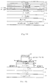
- FIG. 1a the layers of a preferred embodiment heterojunction bipolar transistor (HBT) are shown, which are formed epitaxially. The layers are subsequently etched and contact is made, to form the device shown in FIG. 1b.
- Fig. 2 shows more detail of a portion of FIG. 1b (layers 22-30). Refer to FIGS. 1a-1b and FIG. 2 in the following discussion of the preferred embodiment HBT. The preferred doping levels and thicknesses stated in the description below are approximate values only.
- the device is on a substrate 10 composed of a semi-insulating semiconductor material, such as undoped GaAs.
- a buffer layer 12 typically of undoped GaAs or AlGaAs, is epitaxially formed over the substrate 10.
- a sub-collector layer 14 of n+ GaAs is epitaxially formed over the buffer layer 12.
- the doping of the sub-collector layer 14 is preferably 2x1018 cm ⁇ 3,and the thickness is preferably 1.0 um.
- a collector layer 16 of n- to n type GaAs is epitaxially formed over the sub-collector layer 14.
- the doping of the collector layer 16 is preferably 2x1016 cm ⁇ 3 and the thickness is preferably 1.0 um.
- the dopant preferably used for n type doping, in this device, is Si.
- the base region is formed over the collector layer 16 in two layers, with an optional third layer.
- the first base layer 18 is preferably 1000 - 1500 ⁇ thick. This layer provides low sheet resistivity and low contact resistance.
- a thin, preferably 100 - 500 ⁇ thick, second base layer 20, of p+ GaAs, is epitaxially formed over the first base layer 18 and serves as a diffusion barrier for the first base layer.
- the second base layer doping is lighter than the doping of the first base layer, preferably 1-2x1018 cm ⁇ 3.
- the dopant preferably used for p type doping, in this device, is Zn.
- each layer is chosen considering the diffusion characteristics of each dopant. Generally, a layer of 100 - 500 ⁇ is needed to effectively stop the diffusion of dopants to the p-n junctions. The concentration of dopant in these layers need to be low enough for minimal dopant outdiffusion (i.e. less than 5x1018 cm ⁇ 3 for Zn) while high enough to avoid significantly increased series resistance. The difference between the doping levels of these layers should also be minimized to avoid backdiffusion of minority carriers due to doping concentration profile induced reverse electrical field in the base. A third base layer, with the same doping and thickness as the second base layer 20, may be added between the collector layer 16 and the first base layer 18 to prevent diffusion into the collector during growth.
- n to n+ GaAs emitter stop layer 22 can be epitaxially formed over the second base layer.
- This layer 22 may be doped at 1x1018 cm ⁇ 3 and 100 ⁇ thick.
- the emitter stop layer 22 serves as a barrier between the emitter and the base of the device further isolating the Zn to the base layers, therefore keeping the emitter n type, as needed for proper device performance.
- the emitter layer 24, of n type AlGaAs (the wide bandgap of which provides the heterojunction effect), is epitaxially formed over the emitter stop layer 22 (or over layer 20, if layer 22 is not used), with a preferred doping of 2x1017 cm ⁇ 3 and a preferred thickness of 1000 ⁇ .
- a thin grading layer 26 is epitaxially formed over the emitter layer 24, in which the concentration of Al gradually diminishes (which provides a smooth bandgap transition from AlGaAs to GaAs).
- a first contact layer 28 is formed over the grading layer 26 of n+ GaAs. This layer's doping concentration and thickness are preferably 1x1018 cm ⁇ 3 and 1000 ⁇ , respectively.
- the second contact layer is n+ GaAs with preferable doping of 5x1018 cm ⁇ 3 and thickness of 1500 ⁇ .
- the first contact layer 28 is used as a spacer between the first base layer 18 and the second contact layer 30. The use of this layer lowers the built-in electric field at the emitter-base junction, which is responsible for diffusion enhancement during epitaxial layer growth.
- the structure is anisotropically etched, preferably using a process such as reactive ion etching (RIE) in BCl3 plasma, to form the desired structure, such as the one shown in FIG. 1b.
- RIE reactive ion etching
- the etching exposes the sub-collector layer 14 and the first base layer 18.
- the collector layer 16 may be left unetched on the sub-collector layer 14 and ion implantation may be used to contact the sub-collector layer 14 through the collector layer 16.
- the emitter contact 34, and the collector contacts 36 are preferably formed of layered AuGe/Ni/Au at thicknesses of 500 ⁇ , 140 ⁇ , and 4000 ⁇ , respectively.
- the base contacts 32 are preferably layered Ti/Pt/Au at thicknesses of 500 ⁇ , 250 ⁇ , and 1500 ⁇ , respectively.
- Table 1 below, the preferred ranges for both doping and thicknesses of the different layers of the device may be found. The preferred values may be found in the discussion above. A graphical representation of the typical doping levels of the device is shown in FIG. 3, and may be used for further clarification.
- the described preferred embodiment of the present invention has the advantage that an HBT can be formed with low base resistance, and therefore high operating frequency, by the use of the heavily Zinc doped first base layer 18. If not for the inclusion of the less heavily doped second base layer 20, Zinc diffusion into the emitter 24, driven by heat dissipated by the device and the forward biased base-emitter p-n junction, would degrade the device performance irreversibly over its operating lifetime, producing unstable and unpredictable device performance.
- the p type dopant is referred to as Zn, it could also be materials such as C, Be, Mg, or Mn, and the n type dopant, while preferably silicon, could be a material such as S, or Se.
- the AlGaAs emitter could be any appropriate wide bandgap material such as InGaP and the GaAs could be replaced with a material such as InGaAs or InP.
- the second base layer 20 can be used in relation to any two semiconductor layers where it is desired to control the diffusion of dopants from one layer into the other, for example, in any p-n junction device (such as diodes, transistors, lasers, etc).
Landscapes
- Bipolar Transistors (AREA)
- Electrodes Of Semiconductors (AREA)
Applications Claiming Priority (2)
| Application Number | Priority Date | Filing Date | Title |
|---|---|---|---|
| US672809 | 1991-03-21 | ||
| US07/672,809 US5132764A (en) | 1991-03-21 | 1991-03-21 | Multilayer base heterojunction bipolar transistor |
Publications (3)
| Publication Number | Publication Date |
|---|---|
| EP0504925A2 true EP0504925A2 (de) | 1992-09-23 |
| EP0504925A3 EP0504925A3 (en) | 1993-06-16 |
| EP0504925B1 EP0504925B1 (de) | 2002-10-23 |
Family
ID=24700091
Family Applications (1)
| Application Number | Title | Priority Date | Filing Date |
|---|---|---|---|
| EP92104891A Expired - Lifetime EP0504925B1 (de) | 1991-03-21 | 1992-03-20 | Heteroübergangsbauelement mit einer mehrschichtigen Basis |
Country Status (5)
| Country | Link |
|---|---|
| US (2) | US5132764A (de) |
| EP (1) | EP0504925B1 (de) |
| JP (1) | JPH06132296A (de) |
| KR (1) | KR100289473B1 (de) |
| DE (1) | DE69232826T2 (de) |
Cited By (5)
| Publication number | Priority date | Publication date | Assignee | Title |
|---|---|---|---|---|
| EP0607936A1 (de) * | 1993-01-22 | 1994-07-27 | Hughes Aircraft Company | Elektrisches Übergangsbauelement mit leichtdotiertem Buffergebiet zur präzisen Lokalisierung eines pn-Überganges |
| US5365077A (en) * | 1993-01-22 | 1994-11-15 | Hughes Aircraft Company | Gain-stable NPN heterojunction bipolar transistor |
| EP0597397A3 (de) * | 1992-11-09 | 1995-01-04 | Texas Instruments Inc | Transistor mit Base-Ballastwiderstand. |
| DE19718624A1 (de) * | 1997-05-02 | 1998-11-05 | Daimler Benz Ag | Heterobipolartransistor mit Mehrschicht-Emitterstruktur |
| EP1533849A2 (de) | 2003-11-18 | 2005-05-25 | NEC Compound Semiconductor Devices, Ltd. | Heteroübergang-Bipolartransistor |
Families Citing this family (19)
| Publication number | Priority date | Publication date | Assignee | Title |
|---|---|---|---|---|
| US5132764A (en) * | 1991-03-21 | 1992-07-21 | Texas Instruments Incorporated | Multilayer base heterojunction bipolar transistor |
| US5208184A (en) * | 1991-04-30 | 1993-05-04 | Texas Instruments Incorporated | P-n junction diffusion barrier employing mixed dopants |
| US5352912A (en) * | 1991-11-13 | 1994-10-04 | International Business Machines Corporation | Graded bandgap single-crystal emitter heterojunction bipolar transistor |
| JPH0669227A (ja) * | 1992-05-29 | 1994-03-11 | Texas Instr Inc <Ti> | 化合物半導体のヘテロ接合バイポーラトランジスタ及びその製造方法 |
| JP3117831B2 (ja) * | 1993-02-17 | 2000-12-18 | シャープ株式会社 | 半導体装置 |
| US6107151A (en) * | 1997-05-09 | 2000-08-22 | Research Triangle Institute | Heterojunction bipolar transistor and method of manufacturing |
| JPH10335345A (ja) | 1997-06-04 | 1998-12-18 | Mitsubishi Electric Corp | ヘテロ接合バイポーラトランジスタおよびその製造方法 |
| KR100299097B1 (ko) * | 1998-02-05 | 2001-11-22 | 김효근 | 이종베이스도핑소스를이용한이종접합쌍극자소자구조 |
| JP2000012552A (ja) * | 1998-06-17 | 2000-01-14 | Toshiba Corp | 半導体装置の製造方法及び半導体装置 |
| JP2000068284A (ja) | 1998-08-19 | 2000-03-03 | Sharp Corp | ヘテロ接合バイポーラトランジスタの製造方法及びパワーアンプ |
| US6368930B1 (en) | 1998-10-02 | 2002-04-09 | Ziptronix | Self aligned symmetric process and device |
| TW512529B (en) | 2000-06-14 | 2002-12-01 | Infineon Technologies Ag | Silicon bipolar transistor, circuit arrangement and method for producing a silicon bipolar transistor |
| US6670654B2 (en) * | 2002-01-09 | 2003-12-30 | International Business Machines Corporation | Silicon germanium heterojunction bipolar transistor with carbon incorporation |
| US7019383B2 (en) * | 2003-02-26 | 2006-03-28 | Skyworks Solutions, Inc. | Gallium arsenide HBT having increased performance and method for its fabrication |
| US6784747B1 (en) | 2003-03-20 | 2004-08-31 | Analog Devices, Inc. | Amplifier circuit |
| US6816015B2 (en) * | 2003-03-27 | 2004-11-09 | Analog Devices, Inc. | Amplifier circuit having a plurality of first and second base resistors |
| JP3853341B2 (ja) * | 2003-11-28 | 2006-12-06 | シャープ株式会社 | バイポーラトランジスタ |
| TWI512905B (zh) * | 2012-06-13 | 2015-12-11 | Win Semiconductors Corp | 化合物半導體元件晶圓整合結構 |
| US11133405B2 (en) * | 2018-11-20 | 2021-09-28 | Visual Photonics Epitaxy Co., Ltd. | High ruggedness heterojunction bipolar transistor |
Family Cites Families (17)
| Publication number | Priority date | Publication date | Assignee | Title |
|---|---|---|---|---|
| US4573064A (en) * | 1981-11-02 | 1986-02-25 | Texas Instruments Incorporated | GaAs/GaAlAs Heterojunction bipolar integrated circuit devices |
| US4593305A (en) * | 1983-05-17 | 1986-06-03 | Kabushiki Kaisha Toshiba | Heterostructure bipolar transistor |
| US4794440A (en) * | 1983-05-25 | 1988-12-27 | American Telephone And Telegraph Company, At&T Bell Laboratories | Heterojunction bipolar transistor |
| US4672414A (en) * | 1985-06-28 | 1987-06-09 | Texas Instruments Incorporated | Planar heterojunction bipolar device and method |
| JPS63181486A (ja) * | 1987-01-23 | 1988-07-26 | Hiroshima Univ | 半導体発光装置 |
| KR880010509A (ko) * | 1987-02-11 | 1988-10-10 | 오레그 이. 앨버 | 전계효과 트랜지스터 |
| JPS63276267A (ja) * | 1987-05-08 | 1988-11-14 | Fujitsu Ltd | 半導体装置の製造方法 |
| JPH01238161A (ja) * | 1988-03-18 | 1989-09-22 | Fujitsu Ltd | 半導体装置及びその製造方法 |
| EP0343563A3 (de) * | 1988-05-26 | 1990-05-09 | Siemens Aktiengesellschaft | Bipolartransistorstruktur mit reduziertem Basiswiderstand und Verfahren zur Herstellung eines Basisanschlussbereiches für eine Bipolartransistorstruktur |
| US4987468A (en) * | 1988-06-17 | 1991-01-22 | Xerox Corporation | Lateral heterojunction bipolar transistor (LHBT) and suitability thereof as a hetero transverse junction (HTJ) laser |
| US4948752A (en) * | 1988-08-10 | 1990-08-14 | Itt Corporation | Method of making sagfets on buffer layers |
| JPH02199873A (ja) * | 1989-01-30 | 1990-08-08 | Hitachi Ltd | 半導体装置 |
| DE69032597T2 (de) * | 1990-02-20 | 1999-03-25 | Kabushiki Kaisha Toshiba, Kawasaki, Kanagawa | Bipolartransistor mit Heteroübergang |
| JPH0435037A (ja) * | 1990-05-31 | 1992-02-05 | Toshiba Corp | ヘテロ接合バイポーラトランジスタ |
| US5077231A (en) * | 1991-03-15 | 1991-12-31 | Texas Instruments Incorporated | Method to integrate HBTs and FETs |
| US5132764A (en) * | 1991-03-21 | 1992-07-21 | Texas Instruments Incorporated | Multilayer base heterojunction bipolar transistor |
| US5192698A (en) * | 1992-03-17 | 1993-03-09 | The United State Of America As Represented By The Secretary Of The Air Force | Making staggered complementary heterostructure FET |
-
1991
- 1991-03-21 US US07/672,809 patent/US5132764A/en not_active Expired - Lifetime
-
1992
- 1992-03-19 JP JP4063660A patent/JPH06132296A/ja active Pending
- 1992-03-20 KR KR1019920004601A patent/KR100289473B1/ko not_active Expired - Fee Related
- 1992-03-20 DE DE69232826T patent/DE69232826T2/de not_active Expired - Fee Related
- 1992-03-20 EP EP92104891A patent/EP0504925B1/de not_active Expired - Lifetime
-
1993
- 1993-12-07 US US08/164,641 patent/US5468658A/en not_active Expired - Lifetime
Cited By (9)
| Publication number | Priority date | Publication date | Assignee | Title |
|---|---|---|---|---|
| EP0597397A3 (de) * | 1992-11-09 | 1995-01-04 | Texas Instruments Inc | Transistor mit Base-Ballastwiderstand. |
| EP0607936A1 (de) * | 1993-01-22 | 1994-07-27 | Hughes Aircraft Company | Elektrisches Übergangsbauelement mit leichtdotiertem Buffergebiet zur präzisen Lokalisierung eines pn-Überganges |
| US5365077A (en) * | 1993-01-22 | 1994-11-15 | Hughes Aircraft Company | Gain-stable NPN heterojunction bipolar transistor |
| US5404028A (en) * | 1993-01-22 | 1995-04-04 | Hughes Aircraft Company | Electrical junction device with lightly doped buffer region to precisely locate a p-n junction |
| DE19718624A1 (de) * | 1997-05-02 | 1998-11-05 | Daimler Benz Ag | Heterobipolartransistor mit Mehrschicht-Emitterstruktur |
| EP1533849A2 (de) | 2003-11-18 | 2005-05-25 | NEC Compound Semiconductor Devices, Ltd. | Heteroübergang-Bipolartransistor |
| EP1533849A3 (de) * | 2003-11-18 | 2005-06-08 | NEC Compound Semiconductor Devices, Ltd. | Heteroübergang-Bipolartransistor |
| US7304333B2 (en) | 2003-11-18 | 2007-12-04 | Nec Compound Semiconductor Devices, Ltd. | Semiconductor device |
| CN100454573C (zh) * | 2003-11-18 | 2009-01-21 | 恩益禧电子股份有限公司 | 半导体器件 |
Also Published As
| Publication number | Publication date |
|---|---|
| US5468658A (en) | 1995-11-21 |
| DE69232826T2 (de) | 2003-08-14 |
| EP0504925B1 (de) | 2002-10-23 |
| DE69232826D1 (de) | 2002-11-28 |
| KR100289473B1 (ko) | 2001-06-01 |
| KR920018968A (ko) | 1992-10-22 |
| JPH06132296A (ja) | 1994-05-13 |
| US5132764A (en) | 1992-07-21 |
| EP0504925A3 (en) | 1993-06-16 |
Similar Documents
| Publication | Publication Date | Title |
|---|---|---|
| US5132764A (en) | Multilayer base heterojunction bipolar transistor | |
| US5440152A (en) | Heterojunction bipolar transistor having particular Ge distributions and gradients | |
| US5006912A (en) | Heterojunction bipolar transistor with SiGe | |
| US4959702A (en) | Si-GaP-Si heterojunction bipolar transistor (HBT) on Si substrate | |
| US5426316A (en) | Triple heterojunction bipolar transistor | |
| US6750480B2 (en) | Bipolar transistor with lattice matched base layer | |
| EP0541971B1 (de) | Heteroübergang-Bipolartransistor mit Emitter aus gradiertem Bandabstand-Monokristall | |
| EP1187218B1 (de) | Heteroübergangsbipolartransistor | |
| US6316795B1 (en) | Silicon-carbon emitter for silicon-germanium heterojunction bipolar transistors | |
| KR100270415B1 (ko) | 혼합된 도펀트를 이용한 pn 접합 확산 장벽 및 그 제조 방법 | |
| EP0507454A1 (de) | Heterojunction-Bipolartransistor und dessen Herstellungsverfahren | |
| US6423990B1 (en) | Vertical heterojunction bipolar transistor | |
| EP1636855B1 (de) | Galliumarsenid-hbt und herstellungsverfahren dafür | |
| US5571732A (en) | Method for fabricating a bipolar transistor | |
| US6171920B1 (en) | Method of forming heterojunction bipolar transistor having wide bandgap, low interdiffusion base-emitter junction | |
| JP3874919B2 (ja) | 化合物半導体装置 | |
| Dong et al. | C/sub bc/reduction in InP heterojunction bipolar transistor with selectively implanted collector pedestal | |
| JP3127510B2 (ja) | 半導体装置の製造方法 | |
| US5523594A (en) | Heterojunction bipolar transistor | |
| JP2004022835A (ja) | ヘテロ接合バイポーラトランジスタ用エピタキシャルウェハ及びヘテロ接合バイポーラトランジスタ | |
| JP2803147B2 (ja) | バイポーラトランジスタ | |
| JPH06209008A (ja) | ヘテロ接合バイポーラトランジスタ | |
| KR20010054040A (ko) | 이중 이종접합 쌍극성 트랜지스터 | |
| JPH05299432A (ja) | 化合物半導体装置 | |
| Loga et al. | Fabrication and characterization of circular geometry InGaP/GaAs double heterojunction bipolar transistors |
Legal Events
| Date | Code | Title | Description |
|---|---|---|---|
| PUAI | Public reference made under article 153(3) epc to a published international application that has entered the european phase |
Free format text: ORIGINAL CODE: 0009012 |
|
| AK | Designated contracting states |
Kind code of ref document: A2 Designated state(s): DE FR GB IT NL |
|
| PUAL | Search report despatched |
Free format text: ORIGINAL CODE: 0009013 |
|
| AK | Designated contracting states |
Kind code of ref document: A3 Designated state(s): DE FR GB IT NL |
|
| 17P | Request for examination filed |
Effective date: 19931125 |
|
| 17Q | First examination report despatched |
Effective date: 19950405 |
|
| RIC1 | Information provided on ipc code assigned before grant |
Free format text: 7H 01L 29/737 A, 7H 01L 29/10 B, 7H 01L 21/331 B |
|
| GRAG | Despatch of communication of intention to grant |
Free format text: ORIGINAL CODE: EPIDOS AGRA |
|
| GRAG | Despatch of communication of intention to grant |
Free format text: ORIGINAL CODE: EPIDOS AGRA |
|
| GRAH | Despatch of communication of intention to grant a patent |
Free format text: ORIGINAL CODE: EPIDOS IGRA |
|
| GRAH | Despatch of communication of intention to grant a patent |
Free format text: ORIGINAL CODE: EPIDOS IGRA |
|
| GRAA | (expected) grant |
Free format text: ORIGINAL CODE: 0009210 |
|
| AK | Designated contracting states |
Kind code of ref document: B1 Designated state(s): DE FR GB IT NL |
|
| PG25 | Lapsed in a contracting state [announced via postgrant information from national office to epo] |
Ref country code: IT Free format text: LAPSE BECAUSE OF FAILURE TO SUBMIT A TRANSLATION OF THE DESCRIPTION OR TO PAY THE FEE WITHIN THE PRESCRIBED TIME-LIMIT;WARNING: LAPSES OF ITALIAN PATENTS WITH EFFECTIVE DATE BEFORE 2007 MAY HAVE OCCURRED AT ANY TIME BEFORE 2007. THE CORRECT EFFECTIVE DATE MAY BE DIFFERENT FROM THE ONE RECORDED. Effective date: 20021023 Ref country code: NL Free format text: LAPSE BECAUSE OF FAILURE TO SUBMIT A TRANSLATION OF THE DESCRIPTION OR TO PAY THE FEE WITHIN THE PRESCRIBED TIME-LIMIT Effective date: 20021023 |
|
| REG | Reference to a national code |
Ref country code: GB Ref legal event code: FG4D |
|
| REF | Corresponds to: |
Ref document number: 69232826 Country of ref document: DE Date of ref document: 20021128 |
|
| NLV1 | Nl: lapsed or annulled due to failure to fulfill the requirements of art. 29p and 29m of the patents act | ||
| ET | Fr: translation filed | ||
| PLBE | No opposition filed within time limit |
Free format text: ORIGINAL CODE: 0009261 |
|
| STAA | Information on the status of an ep patent application or granted ep patent |
Free format text: STATUS: NO OPPOSITION FILED WITHIN TIME LIMIT |
|
| 26N | No opposition filed |
Effective date: 20030724 |
|
| PGFP | Annual fee paid to national office [announced via postgrant information from national office to epo] |
Ref country code: GB Payment date: 20070202 Year of fee payment: 16 |
|
| PGFP | Annual fee paid to national office [announced via postgrant information from national office to epo] |
Ref country code: DE Payment date: 20070330 Year of fee payment: 16 |
|
| PGFP | Annual fee paid to national office [announced via postgrant information from national office to epo] |
Ref country code: FR Payment date: 20070301 Year of fee payment: 16 |
|
| GBPC | Gb: european patent ceased through non-payment of renewal fee |
Effective date: 20080320 |
|
| REG | Reference to a national code |
Ref country code: FR Ref legal event code: ST Effective date: 20081125 |
|
| PG25 | Lapsed in a contracting state [announced via postgrant information from national office to epo] |
Ref country code: DE Free format text: LAPSE BECAUSE OF NON-PAYMENT OF DUE FEES Effective date: 20081001 |
|
| PG25 | Lapsed in a contracting state [announced via postgrant information from national office to epo] |
Ref country code: FR Free format text: LAPSE BECAUSE OF NON-PAYMENT OF DUE FEES Effective date: 20080331 |
|
| PG25 | Lapsed in a contracting state [announced via postgrant information from national office to epo] |
Ref country code: GB Free format text: LAPSE BECAUSE OF NON-PAYMENT OF DUE FEES Effective date: 20080320 |