EP0541971B1 - Heteroübergang-Bipolartransistor mit Emitter aus gradiertem Bandabstand-Monokristall - Google Patents
Heteroübergang-Bipolartransistor mit Emitter aus gradiertem Bandabstand-Monokristall Download PDFInfo
- Publication number
- EP0541971B1 EP0541971B1 EP92117404A EP92117404A EP0541971B1 EP 0541971 B1 EP0541971 B1 EP 0541971B1 EP 92117404 A EP92117404 A EP 92117404A EP 92117404 A EP92117404 A EP 92117404A EP 0541971 B1 EP0541971 B1 EP 0541971B1
- Authority
- EP
- European Patent Office
- Prior art keywords
- emitter
- region
- base
- bandgap
- germanium
- Prior art date
- Legal status (The legal status is an assumption and is not a legal conclusion. Google has not performed a legal analysis and makes no representation as to the accuracy of the status listed.)
- Expired - Lifetime
Links
- 239000013078 crystal Substances 0.000 title claims description 18
- 229910052732 germanium Inorganic materials 0.000 claims description 49
- GNPVGFCGXDBREM-UHFFFAOYSA-N germanium atom Chemical compound [Ge] GNPVGFCGXDBREM-UHFFFAOYSA-N 0.000 claims description 48
- 230000007423 decrease Effects 0.000 claims description 24
- 238000000034 method Methods 0.000 claims description 14
- 238000003860 storage Methods 0.000 claims description 13
- 229910000577 Silicon-germanium Inorganic materials 0.000 claims description 7
- LEVVHYCKPQWKOP-UHFFFAOYSA-N [Si].[Ge] Chemical compound [Si].[Ge] LEVVHYCKPQWKOP-UHFFFAOYSA-N 0.000 claims description 5
- 238000004519 manufacturing process Methods 0.000 claims description 4
- 229910045601 alloy Inorganic materials 0.000 claims 3
- 239000000956 alloy Substances 0.000 claims 3
- 239000010703 silicon Substances 0.000 description 27
- 229910052710 silicon Inorganic materials 0.000 description 25
- XUIMIQQOPSSXEZ-UHFFFAOYSA-N Silicon Chemical compound [Si] XUIMIQQOPSSXEZ-UHFFFAOYSA-N 0.000 description 24
- 239000004065 semiconductor Substances 0.000 description 11
- 230000003247 decreasing effect Effects 0.000 description 10
- 229910001218 Gallium arsenide Inorganic materials 0.000 description 9
- 229910052785 arsenic Inorganic materials 0.000 description 9
- RQNWIZPPADIBDY-UHFFFAOYSA-N arsenic atom Chemical compound [As] RQNWIZPPADIBDY-UHFFFAOYSA-N 0.000 description 9
- JBRZTFJDHDCESZ-UHFFFAOYSA-N AsGa Chemical compound [As]#[Ga] JBRZTFJDHDCESZ-UHFFFAOYSA-N 0.000 description 7
- 238000000407 epitaxy Methods 0.000 description 7
- 229910021420 polycrystalline silicon Inorganic materials 0.000 description 7
- 229920005591 polysilicon Polymers 0.000 description 7
- 239000002019 doping agent Substances 0.000 description 6
- 239000012535 impurity Substances 0.000 description 6
- 239000000203 mixture Substances 0.000 description 5
- ZOXJGFHDIHLPTG-UHFFFAOYSA-N Boron Chemical compound [B] ZOXJGFHDIHLPTG-UHFFFAOYSA-N 0.000 description 4
- 239000000969 carrier Substances 0.000 description 4
- 238000005530 etching Methods 0.000 description 4
- 229910052751 metal Inorganic materials 0.000 description 4
- 239000002184 metal Substances 0.000 description 4
- 239000000758 substrate Substances 0.000 description 4
- 229910052796 boron Inorganic materials 0.000 description 3
- 238000010586 diagram Methods 0.000 description 3
- 238000009826 distribution Methods 0.000 description 3
- 239000000463 material Substances 0.000 description 3
- 238000004088 simulation Methods 0.000 description 3
- 229910000927 Ge alloy Inorganic materials 0.000 description 2
- 229910000676 Si alloy Inorganic materials 0.000 description 2
- 230000015556 catabolic process Effects 0.000 description 2
- 238000005229 chemical vapour deposition Methods 0.000 description 2
- 150000001875 compounds Chemical class 0.000 description 2
- 238000013461 design Methods 0.000 description 2
- 230000005684 electric field Effects 0.000 description 2
- 238000001451 molecular beam epitaxy Methods 0.000 description 2
- 229910000980 Aluminium gallium arsenide Inorganic materials 0.000 description 1
- 229910006990 Si1-xGex Inorganic materials 0.000 description 1
- 229910007020 Si1−xGex Inorganic materials 0.000 description 1
- 238000000137 annealing Methods 0.000 description 1
- 230000015572 biosynthetic process Effects 0.000 description 1
- 239000002131 composite material Substances 0.000 description 1
- 239000000470 constituent Substances 0.000 description 1
- 230000000593 degrading effect Effects 0.000 description 1
- 230000001934 delay Effects 0.000 description 1
- 239000010408 film Substances 0.000 description 1
- 238000010348 incorporation Methods 0.000 description 1
- 238000002347 injection Methods 0.000 description 1
- 239000007924 injection Substances 0.000 description 1
- 239000012212 insulator Substances 0.000 description 1
- 238000002955 isolation Methods 0.000 description 1
- 150000004767 nitrides Chemical class 0.000 description 1
- 230000010355 oscillation Effects 0.000 description 1
- 239000000256 polyoxyethylene sorbitan monolaurate Substances 0.000 description 1
- 238000012545 processing Methods 0.000 description 1
- 239000010409 thin film Substances 0.000 description 1
- 238000009827 uniform distribution Methods 0.000 description 1
Images


Classifications
-
- H—ELECTRICITY
- H01—ELECTRIC ELEMENTS
- H01L—SEMICONDUCTOR DEVICES NOT COVERED BY CLASS H10
- H01L29/00—Semiconductor devices adapted for rectifying, amplifying, oscillating or switching, or capacitors or resistors with at least one potential-jump barrier or surface barrier, e.g. PN junction depletion layer or carrier concentration layer; Details of semiconductor bodies or of electrodes thereof ; Multistep manufacturing processes therefor
- H01L29/66—Types of semiconductor device ; Multistep manufacturing processes therefor
- H01L29/68—Types of semiconductor device ; Multistep manufacturing processes therefor controllable by only the electric current supplied, or only the electric potential applied, to an electrode which does not carry the current to be rectified, amplified or switched
- H01L29/70—Bipolar devices
- H01L29/72—Transistor-type devices, i.e. able to continuously respond to applied control signals
- H01L29/73—Bipolar junction transistors
- H01L29/737—Hetero-junction transistors
- H01L29/7371—Vertical transistors
- H01L29/7378—Vertical transistors comprising lattice mismatched active layers, e.g. SiGe strained layer transistors
-
- H—ELECTRICITY
- H01—ELECTRIC ELEMENTS
- H01L—SEMICONDUCTOR DEVICES NOT COVERED BY CLASS H10
- H01L29/00—Semiconductor devices adapted for rectifying, amplifying, oscillating or switching, or capacitors or resistors with at least one potential-jump barrier or surface barrier, e.g. PN junction depletion layer or carrier concentration layer; Details of semiconductor bodies or of electrodes thereof ; Multistep manufacturing processes therefor
- H01L29/66—Types of semiconductor device ; Multistep manufacturing processes therefor
- H01L29/68—Types of semiconductor device ; Multistep manufacturing processes therefor controllable by only the electric current supplied, or only the electric potential applied, to an electrode which does not carry the current to be rectified, amplified or switched
- H01L29/70—Bipolar devices
- H01L29/72—Transistor-type devices, i.e. able to continuously respond to applied control signals
- H01L29/73—Bipolar junction transistors
- H01L29/737—Hetero-junction transistors
-
- Y—GENERAL TAGGING OF NEW TECHNOLOGICAL DEVELOPMENTS; GENERAL TAGGING OF CROSS-SECTIONAL TECHNOLOGIES SPANNING OVER SEVERAL SECTIONS OF THE IPC; TECHNICAL SUBJECTS COVERED BY FORMER USPC CROSS-REFERENCE ART COLLECTIONS [XRACs] AND DIGESTS
- Y10—TECHNICAL SUBJECTS COVERED BY FORMER USPC
- Y10S—TECHNICAL SUBJECTS COVERED BY FORMER USPC CROSS-REFERENCE ART COLLECTIONS [XRACs] AND DIGESTS
- Y10S438/00—Semiconductor device manufacturing: process
- Y10S438/936—Graded energy gap
Definitions
- the present invention relates to a heterojunction bipolar transistor, and more particularly to a bipolar transistor having a graded bandgap emitter region.
- Bipolar transistors are important components in, for example, logic circuits, communications systems, and microwave devices.
- a bipolar transistor is essentially a three terminal device having three regions, an emitter, base and collector region, wherein the emitter and collector regions are of one conductivity type and the base is of another.
- a wide bandgap heterojunction bipolar transistor is described.
- the transistor includes a collector region of gallium arsenide, a base region of germanium and an emitter region having a semiconductor layer of mixed crystal of silicon and germanium.
- the mixed crystal semiconductor layer may have a uniform distribution of silicon in germanium or a graded distribution of silicon. If the graded distribution is provided, the content of silicon increases with distance from the interface between the base and emitter regions.
- the silicon is added to the emitter region in order to increase the bandgap of the emitter region so that it is larger than the base bandgap.
- Patent Abstract of Japan, vol. 10, no. 251 (E-432), August 28, 1986, & JP-A-61 79 255 describes the manufacturing of a hetero-junction transistor.
- a collector electrode easily by a method wherein a semi-conductor film of a different kind is shaped between a collector layer and a connecting layer for the collector layer, only the collector layer and the connecting layer for the collector layer are etched selectively, only the collector layer is etched, and a collector connecting layer is formed.
- a mask is formed and the GaAs emitter connecting layer is shaped through etching, and Mg is implanted and activated to form a P-external base.
- a collector electrode can be formed easily to a hetero-junction transistor, and characteristic distribution in a wafer is improved.
- Patents Abstract of Japan, vol. 15, no. 265 (E-1086), July 5, 1991, & JP-A-3 88 335 a semiconductor device is described, to achieve a high speed and low power consumption by interposing a compound semiconductor thin film for wide energy band gap wherein the composition for widening an energy band gap continuously toward a base from and emitter becomes larger in a graded mode and which serves the role of an etching stopping layer between a compound-semiconductor emitter layer and a compound semiconductor base layer.
- a compound-seciconductor layer for wide energy band gap is provided between a compound-semiconductor emitter layer and a compound-semiconductor base layer.
- the composition for widening an energy band gap continuously toward the bse from the emitter becomes larger in a graded mode.
- the semiconductor layer serves the rold of an etching stopping layer.
- the constituent material of the emitter layer E is n-type GaAs.
- the transistors mentioned in the above three documents have a graded emitter layer having a bandgap decreasing towards the emitter contact, i.e., decreasing as the distance from the base region increases.
- a bipolar transistor having a graded silicon/-germanium base is fabricated.
- the silicon/germanium base is epitaxially grown on an N-type collector, which is formed on a silicon substrate.
- the emitter region is formed on the base.
- a window is opened and polysilicon is deposited.
- the polysilicon is heavily doped with an N-type dopant, such as arsenic.
- an N-type dopant such as arsenic.
- the arsenic is implanted in the polysilicon and then a high temperature anneal cycle (e.g. 850°C for 15 minutes) is used to diffuse the arsenic through the polysilicon, the polysilicon/silicon interface of the emitter and into the base. This process enables bases of approximately 60 nm (600 Angstroms) to be formed.
- the above-described process places a limitation on how thin the bases can be fabricated.
- This limitation is due to the fact that the high temperature anneal cycle causes the P-type dopant, e.g. boron, in the base to diffuse thereby causing the base width to increase. Therefore, there is a limitation as to how thin the bases can be fabricated when the emitter is formed and contacted by polysilicon.
- a need to increase device performance Further, a need still exists to reduce the width of a base region in the device.
- a heterojunction transistor having a first region of a first conductivity type, a second region of a second conductivity type formed on the first region and a third region of the first conductivity type formed on the second region is provided.
- the third region has a bandgap which decreases as the distance from the second region increases.
- a heterojunction bipolar transistor including a first region of a first conductivity type, a second region of a second conductivity type formed on the first region and a third region of the first conductivity type formed on the second region.
- the third region has a contact and the second region and third region define a junction.
- the second and third regions have a first and second bandgap, respectively, wherein the second bandgap is narrower at the contact than the first bandgap at the junction.
- a method for reducing charge storage in the emitter region of a bipolar transistor includes the step of grading the bandgap of the emitter region such that the bandgap decreases as the distance to the emitter contact decreases.
- the grading of the emitter bandgap is accomplished by adding an increasing amount of germanium to the emitter region.
- a heterojunction bipolar transistor having a single-crystal emitter is desirous, since a thinner base may be fabricated with such a design, thereby improving the cut-off frequency performance of the transistor.
- one disadvantage of the single-crystal emitter is that the thinner the emitter, the higher the base current and the lower the current gain.
- an emitter is approximately 30 nm or less, the base current is very large and the current gain is unacceptably low.
- current gain collector current ⁇ base current.
- a preferable current gain is approximately 100). Therefore, in order to decrease the base current, a thick single-crystal emitter is formed, e.g. 200 nm.
- a thicker emitter leads to another problem, however, and that is increased emitter charge storage.
- the cut-off frequency (f ⁇ ) decreases and, device performance is degraded.
- the emitter charge storage is decreased by grading the bandgap of the single-crystal emitter.
- the transistor includes an emitter contact 102, a single-crystal emitter region 104, a base region 106, and a collector region 108. (Each of these regions is known in the art. In addition, it is known in the art that there are quasi-neutral regions within the emitter and base region (not shown) and that there is virtually no electrostatic electric field in the quasi-neutral regions).
- emitter contact 102 is, for example, metal and emitter region 104 is approximately 200 nm thick and would be fabricated of a silicon/germanium alloy.
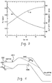
- the bandgap of the quasi-neutral region of the emitter is graded using as one example, a germanium profile 110 illustrated in FIG. 1.
- the germanium profile starts at approximately 0% and increases to 20% as the distance from the base region increases.
- This bandgap grading results in a quasi- electric field which drives the minority carriers towards the emitter contact thereby decreasing emitter charge storage.
- the germanium is added to the emitter region, the base current increases and thus, the current gain decreases to significantly below 80, thereby degrading device performance.
- germanium is also added to base region 106.
- the base is approximately 25 nm and a graded profile of germanium 200 (FIG. 2) is added to the base.
- FIG. 2 in one example, the germanium profile in the base starts at approximately 5% and increases to 23% as the distance to the collector region decreases.
- the grading in the base advantageously increases the collector current at a given emitter-base voltage which increases the current gain.
- the grading profiles associated with the quasi-neutral region of the emitter and the base enable the current gain to remain at, for instance, approximately 80.
- an emitter bandgap 402 decreases as the distance from an emitter-base junction 404 increases and the distance to the emitter contact 102 decreases.
- Ec represents the conductance band
- Ev represents the valence band.
- the emitter bandgap is decreased by a value of 0.15 eV (electron volts), which is reflected in FIG. 4 as ⁇ E gE . This narrowing of the bandgap creates a quasi-electric field which sweeps the carriers towards the metal emitter contact 102, thereby reducing charge storage in the emitter.
- a base bandgap 406 decreases as the distance from emitter-base junction 404 increases and the distance to the base-collector junction (not shown) decreases.
- the base bandgap is decreased by a value 0.17eV, which is reflected as ⁇ E gB .
- the bandgap of the emitter is narrower at the emitter contact than the bandgap of the base at the emitter-base junction 404.
- the emitter bandgap equals 0.95eV at emitter contact 102, while the base bandgap at emitter-base junction 404 is 1.06eV.
- the narrowing of the emitter bandgap is achieved, in accordance with the principles of the present invention, by grading the emitter bandgap with germanium. Some emitter bandgap narrowing caused by the grading of the dopant profile of the emitter may also occur.
- bandgap grading may be enhanced, especially when a high concentration of dopant is used.
- FIG. 6 One example of a device which could be structured in accordance with the principles of the present invention is depicted in FIG. 6.
- an N+ silicon layer 602 is formed with a thickness of 1000 nm and is heavily doped with arsenic.
- an N-silicon layer 604 with a thickness of 400 nm and a 1x10 16 cm -3 impurity concentration of arsenic is formed by epitaxy.
- the N+ silicon layer 602 and N-silicon layer 604 form the collector region 108 (FIG. 1).
- deep trench isolation (not shown) between the devices is formed.
- a base region of P silicon/germanium layer 606 is formed by low temperature epitaxy such as MBE (Molecular Beam Epitaxy) or UHV/CVD (Ultra-High Vacuum/Chemical Vapor Deposition).
- the base has a final thickness of 25 nm and a boron impurity concentration of typically 1x10 19 cm -3 .
- an increasing amount of germanium is added to the silicon at selective points in the base.
- a grading profile of 5%-23% of germanium is added to the base wherein the amount of germanium increases as the distance to the collector region decreases.
- the emitter region is grown by defining an emitter window by known methods and then using low-temperature epitaxy to deposit an N+ silicon/germanium layer 608 having a thickness of 200 nm and an arsenic impurity concentration of 1x10 19 cm -3 .
- a material 610 is an insulator such as oxide, nitride, or composite stack.
- an increasing amount of germanium is added to the emitter.
- a grading profile of 0-20% of germanium is added to the emitter wherein the amount of germanium increases as the distance to the emitter contact decreases and the distance from the emitter-base junction increases.
- device performance is significantly enhanced. While the structure of an N-P-N transistor is described herein, the invention is also applicable to P-N-P transistors. Very heavily doped emitters of silicon germanium P-N-P transistors can be grown by low-temperature temperature epitaxy and the presence of germanium in the emitters counteracts the strain associated with the large concentration of boron atoms.
- FIG. 7 Another example of a device structured in accordance with the principles of the present invention is depicted in FIG. 7.
- a heavily doped (with e.g. arsenic) N+ silicon layer 702 having a thickness of typically 1000 nm is formed on a P-type silicon substrate 700.
- an N-silicon layer 704 with a thickness of 400 nm and a 1x10 16 cm -3 impurity concentration of arsenic is formed by epitaxy.
- a P-type base region of a silicon/germanium layer 706 is formed by low- temperature epitaxy.
- the base has a thickness of 25 nm and a boron impurity concentration of 1x10 19 cm -3 .
- an increasing amount of germanium is added to the silicon at selective points in the base.
- a grading profile of 5%-23% of germanium is added to the base wherein the amount of germanium increases as the distance to the collector region decreases.
- a single-crystal emitter having an N+ silicon/germanium alloy layer 707 having a thickness of 100-200 nm and an impurity concentration of 5x10 18 -1x10 19 cm -3 is formed thereon by low-temperature epitaxy.
- the electrical emitter dimensions are defined by an extrinsic P+ base 708 which is formed on either side of an emitter contact window 710. Thereafter, a contact window 710 is opened on top of emitter 707.
- the insulated layers 714 isolate the emitter contact from the extrinsic base.
- an increasing amount of germanium is added to the emitter.
- a grading profile of 0-20% of germanium is added to the emitter wherein the amount of germanium increases as the distance to the emitter contact decreases and the distance from the emitter-base junction increases.
- this grading profile may be used whenever the current gain needs to be decreased. For instance, as is known, if the current gain is too high (e.g. significantly greater than 100), then the breakdown voltage BVceo may decrease to unacceptable levels. Thus, the emitter bandgap grading profile of the present invention may be used to reduce the current gain and establish an acceptable level for the breakdown voltage BVceo.
Claims (8)
- Ein Bipolartransistor mit Heteroübergang (100), folgendes umfassend:einen Kollektorbereich (108) des Typs n;einen Basisbereich (106) des Typs p, der auf dem genannten Kollektorbereich gebildet wurde;einen Einkristall-Emitterbereich (104) des Typs n, hergestellt aus einer Silizium-Germanium-Legierung, der auf dem genannten Basisbereich gebildet wurde, wobei der genannte Einkristall-Emitterbereich einen Bandabstand aufweist, der mit zunehmendem Abstand zum Emitter-Basis-Übergang (404) abnimmt, wobei der genannte Bandabstand an allen Punkten innerhalb des genannten Emitterbereichs schmäler ist, als an dem genannten Emitter-Basis-Übergang;
- Der Bipolartransistor mit Heteroübergang nach Anspruch 1, bei dem der genannte Basisbereich einen Bandabstand aufweist, der genannte Emitterbereich über einen darauf gebildeten Kontakt verfügt und der Bandabstand des genannten Emitterbereichs an dem genannten Kontakt schmäler ist, als der genannte Bandabstand des genannten Basisbereichs an dem genannten Übergang.
- Der Transistor mit Heteroübergang nach Anspruch 2, bei dem der genannte Bandabstand des genannten Basisbereichs graduiert ist.
- Der Transistor mit Heteroübergang nach einem jeden der Ansprüche 1 bis 3, bei dem der genannte Emitterbereich eine Dicke von über 30 nm aufweist.
- Ein Verfahren zur Herstellung eines Bipolartransistors mit Heteroübergang (100) nach einem der Ansprüche 1 bis 4, mit einem Einkristall-Emitterbereich (104), umfassend einen Emitterkontakt (102), einen Basisbereich (106) und einen Kollektorbereich (108), umfassend den Schritt des Abstufens eines Bandabstands in dem genannten Emitterbereich, wobei der genannte Emitterbereich aus einer Silizium-Germanium-Legierung hergestellt ist und der genannte Graduierungsschritt die Zugabe einer zunehmenden Menge Germanium zu dem genannten Emitterbereich beinhaltet, wenn der Abstand zu dem genannten Basisbereich zunimmt, wodurch der genannte Bandabstand in dem genannten Emitterbereich mit zunehmendem Abstand zum Emitter-Basis-Übergang (404) abnimmt, wodurch die Ladungsspeicherung in dem genannten Emitterbereich reduziert wird, wobei der genannte Bandabstand an allen Punkten innerhalb des genannten Emitterbereichs schmäler wird, als an dem genannten Emitter-Basis-Übergang (404).
- Das Verfahren nach Anspruch 5, bei dem die Menge des genannten Germaniums von 0% auf 20% zunimmt.
- Das Verfahren nach einem der Ansprüche 5 bis 6, bei dem der genannte Basisbereich aus einer Silizium-Germanium-Legierung hergestellt wurde, bei der mit abnehmendem Abstand zu dem genannten Kollektorbereich eine zunehmende Menge Germanium zugegeben wird, wodurch der genannte Bandabstand des genannten Basisbereichs mit abnehmendem Abstand zu dem genannten Kollektorbereich abnimmt.
- Das Verfahren nach Anspruch 7, bei dem die Menge des genannten Germaniums von 5% Germanium auf 23% Germanium zunimmt.
Applications Claiming Priority (2)
| Application Number | Priority Date | Filing Date | Title |
|---|---|---|---|
| US07/792,493 US5352912A (en) | 1991-11-13 | 1991-11-13 | Graded bandgap single-crystal emitter heterojunction bipolar transistor |
| US792493 | 1991-11-13 |
Publications (3)
| Publication Number | Publication Date |
|---|---|
| EP0541971A2 EP0541971A2 (de) | 1993-05-19 |
| EP0541971A3 EP0541971A3 (en) | 1993-09-29 |
| EP0541971B1 true EP0541971B1 (de) | 2000-08-02 |
Family
ID=25157071
Family Applications (1)
| Application Number | Title | Priority Date | Filing Date |
|---|---|---|---|
| EP92117404A Expired - Lifetime EP0541971B1 (de) | 1991-11-13 | 1992-10-12 | Heteroübergang-Bipolartransistor mit Emitter aus gradiertem Bandabstand-Monokristall |
Country Status (4)
| Country | Link |
|---|---|
| US (1) | US5352912A (de) |
| EP (1) | EP0541971B1 (de) |
| JP (1) | JPH07118480B2 (de) |
| DE (1) | DE69231310T2 (de) |
Families Citing this family (32)
| Publication number | Priority date | Publication date | Assignee | Title |
|---|---|---|---|---|
| CA2062134C (en) * | 1991-05-31 | 1997-03-25 | Ibm | Heteroepitaxial layers with low defect density and arbitrary network parameter |
| JP2778553B2 (ja) * | 1995-09-29 | 1998-07-23 | 日本電気株式会社 | 半導体装置およびその製造方法 |
| US6750484B2 (en) * | 1996-12-09 | 2004-06-15 | Nokia Corporation | Silicon germanium hetero bipolar transistor |
| DE19755979A1 (de) * | 1996-12-09 | 1999-06-10 | Inst Halbleiterphysik Gmbh | Silizium-Germanium-Heterobipolartransistor |
| US5976941A (en) * | 1997-06-06 | 1999-11-02 | The Whitaker Corporation | Ultrahigh vacuum deposition of silicon (Si-Ge) on HMIC substrates |
| TW567559B (en) * | 1999-06-23 | 2003-12-21 | Hitachi Ltd | Semiconductor device |
| US6251738B1 (en) | 2000-01-10 | 2001-06-26 | International Business Machines Corporation | Process for forming a silicon-germanium base of heterojunction bipolar transistor |
| US6573539B2 (en) | 2000-01-10 | 2003-06-03 | International Business Machines Corporation | Heterojunction bipolar transistor with silicon-germanium base |
| DE10002364A1 (de) * | 2000-01-20 | 2001-08-02 | Infineon Technologies Ag | Silizium-Germanium-Bipolartranistor mit optimiertem Germaniumprofil |
| TW512529B (en) * | 2000-06-14 | 2002-12-01 | Infineon Technologies Ag | Silicon bipolar transistor, circuit arrangement and method for producing a silicon bipolar transistor |
| JP4882141B2 (ja) * | 2000-08-16 | 2012-02-22 | 富士通株式会社 | ヘテロバイポーラトランジスタ |
| JP2002164533A (ja) * | 2000-11-29 | 2002-06-07 | Showa Denko Kk | 化合物半導体積層構造体及びそれを用いたバイポーラトランジスタ |
| US20020163013A1 (en) | 2000-09-11 | 2002-11-07 | Kenji Toyoda | Heterojunction bipolar transistor |
| US6555891B1 (en) | 2000-10-17 | 2003-04-29 | International Business Machines Corporation | SOI hybrid structure with selective epitaxial growth of silicon |
| US6362065B1 (en) | 2001-02-26 | 2002-03-26 | Texas Instruments Incorporated | Blocking of boron diffusion through the emitter-emitter poly interface in PNP HBTs through use of a SiC layer at the top of the emitter epi layer |
| EP1265294A3 (de) * | 2001-06-07 | 2004-04-07 | Matsushita Electric Industrial Co., Ltd. | Heteroübergang-Bipolartransistor |
| US6555852B1 (en) * | 2002-01-17 | 2003-04-29 | Agere Systems Inc. | Bipolar transistor having an emitter comprised of a semi-insulating material |
| US20030230778A1 (en) * | 2002-01-30 | 2003-12-18 | Sumitomo Mitsubishi Silicon Corporation | SOI structure having a SiGe Layer interposed between the silicon and the insulator |
| US7170112B2 (en) * | 2002-10-30 | 2007-01-30 | International Business Machines Corporation | Graded-base-bandgap bipolar transistor having a constant—bandgap in the base |
| JP4306266B2 (ja) | 2003-02-04 | 2009-07-29 | 株式会社Sumco | 半導体基板の製造方法 |
| JP3653087B2 (ja) * | 2003-07-04 | 2005-05-25 | 三菱重工業株式会社 | Dc/dcコンバータ |
| JP2005072157A (ja) * | 2003-08-22 | 2005-03-17 | Mitsubishi Heavy Ind Ltd | 電力変換装置 |
| US7544577B2 (en) * | 2005-08-26 | 2009-06-09 | International Business Machines Corporation | Mobility enhancement in SiGe heterojunction bipolar transistors |
| JP4829566B2 (ja) * | 2005-08-30 | 2011-12-07 | 株式会社日立製作所 | 半導体装置及びその製造方法 |
| US20070102729A1 (en) * | 2005-11-04 | 2007-05-10 | Enicks Darwin G | Method and system for providing a heterojunction bipolar transistor having SiGe extensions |
| US7651919B2 (en) * | 2005-11-04 | 2010-01-26 | Atmel Corporation | Bandgap and recombination engineered emitter layers for SiGe HBT performance optimization |
| US7300849B2 (en) * | 2005-11-04 | 2007-11-27 | Atmel Corporation | Bandgap engineered mono-crystalline silicon cap layers for SiGe HBT performance enhancement |
| US7439558B2 (en) | 2005-11-04 | 2008-10-21 | Atmel Corporation | Method and system for controlled oxygen incorporation in compound semiconductor films for device performance enhancement |
| US7294869B2 (en) * | 2006-04-04 | 2007-11-13 | International Business Machines Corporation | Silicon germanium emitter |
| US9455338B1 (en) * | 2012-12-14 | 2016-09-27 | Altera Corporation | Methods for fabricating PNP bipolar junction transistors |
| CN103441141B (zh) * | 2013-07-29 | 2016-08-10 | 北京工业大学 | 超宽温区高热稳定性微波功率SiGe异质结双极晶体管 |
| US11682718B2 (en) | 2021-04-15 | 2023-06-20 | International Business Machines Corporation | Vertical bipolar junction transistor with all-around extrinsic base and epitaxially graded intrinsic base |
Citations (1)
| Publication number | Priority date | Publication date | Assignee | Title |
|---|---|---|---|---|
| JPS6179255A (ja) * | 1984-09-27 | 1986-04-22 | Toshiba Corp | ヘテロ接合トランジスタの製造方法 |
Family Cites Families (13)
| Publication number | Priority date | Publication date | Assignee | Title |
|---|---|---|---|---|
| US3275986A (en) * | 1962-06-14 | 1966-09-27 | Gen Dynamics Corp | Pattern recognition systems |
| US3275906A (en) * | 1962-08-20 | 1966-09-27 | Nippon Electric Co | Multiple hetero-layer composite semiconductor device |
| US4794440A (en) * | 1983-05-25 | 1988-12-27 | American Telephone And Telegraph Company, At&T Bell Laboratories | Heterojunction bipolar transistor |
| US4768074A (en) * | 1984-11-20 | 1988-08-30 | Kabushiki Kaisha Toshiba | Heterojunction bipolar transistor having an emitter region with a band gap greater than that of a base region |
| US4691215A (en) * | 1985-01-09 | 1987-09-01 | American Telephone And Telegraph Company | Hot electron unipolar transistor with two-dimensional degenerate electron gas base with continuously graded composition compound emitter |
| JPS62165975A (ja) * | 1986-01-17 | 1987-07-22 | Nec Corp | ヘテロ構造バイポ−ラ・トランジスタ |
| US4716445A (en) * | 1986-01-17 | 1987-12-29 | Nec Corporation | Heterojunction bipolar transistor having a base region of germanium |
| US4771326A (en) * | 1986-07-09 | 1988-09-13 | Texas Instruments Incorporated | Composition double heterojunction transistor |
| US4887134A (en) * | 1986-09-26 | 1989-12-12 | Canon Kabushiki Kaisha | Semiconductor device having a semiconductor region in which either the conduction or valence band remains flat while bandgap is continuously graded |
| JP2804095B2 (ja) * | 1989-07-10 | 1998-09-24 | 株式会社東芝 | ヘテロ接合バイボーラトランジスタ |
| US4959702A (en) * | 1989-10-05 | 1990-09-25 | Motorola, Inc. | Si-GaP-Si heterojunction bipolar transistor (HBT) on Si substrate |
| JPH05144834A (ja) * | 1991-03-20 | 1993-06-11 | Hitachi Ltd | バイポーラトランジスタ及びその製造方法 |
| US5132764A (en) * | 1991-03-21 | 1992-07-21 | Texas Instruments Incorporated | Multilayer base heterojunction bipolar transistor |
-
1991
- 1991-11-13 US US07/792,493 patent/US5352912A/en not_active Expired - Lifetime
-
1992
- 1992-10-09 JP JP4297671A patent/JPH07118480B2/ja not_active Expired - Lifetime
- 1992-10-12 DE DE69231310T patent/DE69231310T2/de not_active Expired - Lifetime
- 1992-10-12 EP EP92117404A patent/EP0541971B1/de not_active Expired - Lifetime
Patent Citations (1)
| Publication number | Priority date | Publication date | Assignee | Title |
|---|---|---|---|---|
| JPS6179255A (ja) * | 1984-09-27 | 1986-04-22 | Toshiba Corp | ヘテロ接合トランジスタの製造方法 |
Non-Patent Citations (3)
| Title |
|---|
| CHANG ET AL, IEEE, vol. EDL-8, no. 7, July 1987 (1987-07-01), pages 303 - 305 * |
| PATENT ABSTRACTS OF JAPAN vol. 010, no. 251 (E - 432) 28 August 1986 (1986-08-28) * |
| PATTON ET AL, IEEE ED, vol. EDL 10, no. 12, December 1987 (1987-12-01), pages 534 - 536 * |
Also Published As
| Publication number | Publication date |
|---|---|
| JPH07118480B2 (ja) | 1995-12-18 |
| DE69231310T2 (de) | 2001-02-15 |
| US5352912A (en) | 1994-10-04 |
| EP0541971A3 (en) | 1993-09-29 |
| DE69231310D1 (de) | 2000-09-07 |
| EP0541971A2 (de) | 1993-05-19 |
| JPH07193078A (ja) | 1995-07-28 |
Similar Documents
| Publication | Publication Date | Title |
|---|---|---|
| EP0541971B1 (de) | Heteroübergang-Bipolartransistor mit Emitter aus gradiertem Bandabstand-Monokristall | |
| US5656514A (en) | Method for making heterojunction bipolar transistor with self-aligned retrograde emitter profile | |
| EP0445475B1 (de) | Bipolartransistor mit Heteroübergang | |
| US5426316A (en) | Triple heterojunction bipolar transistor | |
| US5006912A (en) | Heterojunction bipolar transistor with SiGe | |
| US7566921B2 (en) | Silicon germanium emitter | |
| US4958208A (en) | Bipolar transistor with abrupt potential discontinuity in collector region | |
| Rieh et al. | Performance and design considerations for high speed SiGe HBTs of f/sub T//f/sub max/= 375 GHz/210 GHz | |
| Crabbe et al. | 73-GHz self-aligned SiGe-base bipolar transistors with phosphorus-doped polysilicon emitters | |
| JP2804095B2 (ja) | ヘテロ接合バイボーラトランジスタ | |
| US6861324B2 (en) | Method of forming a super self-aligned hetero-junction bipolar transistor | |
| JP2001338930A (ja) | 半導体装置および半導体製造方法 | |
| US5448087A (en) | Heterojunction bipolar transistor with graded base doping | |
| US7170112B2 (en) | Graded-base-bandgap bipolar transistor having a constant—bandgap in the base | |
| US20020020852A1 (en) | Silicon-germanium base and a heterojunction bipoplar transistor with the silicon-germanium base | |
| Streit et al. | Effect of exponentially graded base doping on the performance of GaAs/AlGaAs heterojunction bipolar transistors | |
| Ida et al. | Enhancement of f/sub max/in InP/InGaAs HBTs by selective MOCVD growth of heavily-doped extrinsic base regions | |
| Vook et al. | Double-diffused graded SiGe-base bipolar transistors | |
| Houston | High-frequency heterojunction bipolar transistor device design and technology | |
| Enquist et al. | Self-aligned AlGaAs/GaAs HBT with selectively regrown OMVPE emitter | |
| Shimawaki et al. | High-f/sub max/AlGaAs/InGaAs and AlGaAs/GaAs HBTs fabricated with MOMBE selective growth in extrinsic base regions | |
| Pelouard et al. | Double-heterojunction GaAlInAs/GaInAs bipolar transistor grown by molecular beam epitaxy | |
| Chen et al. | Submicrometer Si and Si-Ge epitaxial-base double-poly self-aligned bipolar transistors | |
| JP2963704B2 (ja) | ヘテロ接合バイポーラトランジスタの製造方法 | |
| JP3183882B2 (ja) | ヘテロ接合バイポーラトランジスタ |
Legal Events
| Date | Code | Title | Description |
|---|---|---|---|
| PUAI | Public reference made under article 153(3) epc to a published international application that has entered the european phase |
Free format text: ORIGINAL CODE: 0009012 |
|
| AK | Designated contracting states |
Kind code of ref document: A2 Designated state(s): DE FR GB |
|
| PUAL | Search report despatched |
Free format text: ORIGINAL CODE: 0009013 |
|
| AK | Designated contracting states |
Kind code of ref document: A3 Designated state(s): DE FR GB |
|
| 17P | Request for examination filed |
Effective date: 19930918 |
|
| 17Q | First examination report despatched |
Effective date: 19951201 |
|
| GRAG | Despatch of communication of intention to grant |
Free format text: ORIGINAL CODE: EPIDOS AGRA |
|
| GRAG | Despatch of communication of intention to grant |
Free format text: ORIGINAL CODE: EPIDOS AGRA |
|
| GRAH | Despatch of communication of intention to grant a patent |
Free format text: ORIGINAL CODE: EPIDOS IGRA |
|
| GRAH | Despatch of communication of intention to grant a patent |
Free format text: ORIGINAL CODE: EPIDOS IGRA |
|
| GRAA | (expected) grant |
Free format text: ORIGINAL CODE: 0009210 |
|
| AK | Designated contracting states |
Kind code of ref document: B1 Designated state(s): DE FR GB |
|
| REF | Corresponds to: |
Ref document number: 69231310 Country of ref document: DE Date of ref document: 20000907 |
|
| PGFP | Annual fee paid to national office [announced via postgrant information from national office to epo] |
Ref country code: GB Payment date: 20001003 Year of fee payment: 9 |
|
| ET | Fr: translation filed | ||
| PLBE | No opposition filed within time limit |
Free format text: ORIGINAL CODE: 0009261 |
|
| STAA | Information on the status of an ep patent application or granted ep patent |
Free format text: STATUS: NO OPPOSITION FILED WITHIN TIME LIMIT |
|
| 26N | No opposition filed | ||
| PG25 | Lapsed in a contracting state [announced via postgrant information from national office to epo] |
Ref country code: GB Free format text: LAPSE BECAUSE OF NON-PAYMENT OF DUE FEES Effective date: 20011012 |
|
| REG | Reference to a national code |
Ref country code: GB Ref legal event code: IF02 |
|
| GBPC | Gb: european patent ceased through non-payment of renewal fee |
Effective date: 20011012 |
|
| PGFP | Annual fee paid to national office [announced via postgrant information from national office to epo] |
Ref country code: DE Payment date: 20101028 Year of fee payment: 19 |
|
| PGFP | Annual fee paid to national office [announced via postgrant information from national office to epo] |
Ref country code: FR Payment date: 20111028 Year of fee payment: 20 |
|
| REG | Reference to a national code |
Ref country code: DE Ref legal event code: R071 Ref document number: 69231310 Country of ref document: DE |
|
| REG | Reference to a national code |
Ref country code: DE Ref legal event code: R071 Ref document number: 69231310 Country of ref document: DE |
|
| REG | Reference to a national code |
Ref country code: DE Ref legal event code: R081 Ref document number: 69231310 Country of ref document: DE Owner name: GLOBALFOUNDRIES INC., KY Free format text: FORMER OWNER: INTERNATIONAL BUSINESS MACHINES CORPORATION, ARMONK, NY, US Ref country code: DE Ref legal event code: R082 Ref document number: 69231310 Country of ref document: DE Representative=s name: RICHARDT PATENTANWAELTE PARTG MBB, DE Ref country code: DE Ref legal event code: R081 Ref document number: 69231310 Country of ref document: DE Owner name: GLOBALFOUNDRIES INC., KY Free format text: FORMER OWNER: INTERNATIONAL BUSINESS MACHINES CORPORATION, ARMONK, N.Y., US |
|
| REG | Reference to a national code |
Ref country code: DE Ref legal event code: R082 Ref document number: 69231310 Country of ref document: DE Representative=s name: RICHARDT PATENTANWAELTE PARTG MBB, DE Ref country code: DE Ref legal event code: R081 Ref document number: 69231310 Country of ref document: DE Owner name: GLOBALFOUNDRIES INC., KY Free format text: FORMER OWNER: GLOBALFOUNDRIES US 2 LLC (N.D.GES.DES STAATES DELAWARE), HOPEWELL JUNCTION, N.Y., US |
|
| REG | Reference to a national code |
Ref country code: FR Ref legal event code: TP Owner name: GLOBALFOUNDRIES INC., GB Effective date: 20160829 |