EP0503769A1 - Leiterrahmen und in Harz versiegelte Halbleitervorrichtung dafür - Google Patents
Leiterrahmen und in Harz versiegelte Halbleitervorrichtung dafür Download PDFInfo
- Publication number
- EP0503769A1 EP0503769A1 EP19920301150 EP92301150A EP0503769A1 EP 0503769 A1 EP0503769 A1 EP 0503769A1 EP 19920301150 EP19920301150 EP 19920301150 EP 92301150 A EP92301150 A EP 92301150A EP 0503769 A1 EP0503769 A1 EP 0503769A1
- Authority
- EP
- European Patent Office
- Prior art keywords
- semiconductor element
- die pad
- element mounting
- dimples
- mounting die
- Prior art date
- Legal status (The legal status is an assumption and is not a legal conclusion. Google has not performed a legal analysis and makes no representation as to the accuracy of the status listed.)
- Granted
Links
Images


Classifications
-
- H—ELECTRICITY
- H10—SEMICONDUCTOR DEVICES; ELECTRIC SOLID-STATE DEVICES NOT OTHERWISE PROVIDED FOR
- H10W—GENERIC PACKAGES, INTERCONNECTIONS, CONNECTORS OR OTHER CONSTRUCTIONAL DETAILS OF DEVICES COVERED BY CLASS H10
- H10W70/00—Package substrates; Interposers; Redistribution layers [RDL]
- H10W70/40—Leadframes
- H10W70/411—Chip-supporting parts, e.g. die pads
-
- H—ELECTRICITY
- H10—SEMICONDUCTOR DEVICES; ELECTRIC SOLID-STATE DEVICES NOT OTHERWISE PROVIDED FOR
- H10W—GENERIC PACKAGES, INTERCONNECTIONS, CONNECTORS OR OTHER CONSTRUCTIONAL DETAILS OF DEVICES COVERED BY CLASS H10
- H10W72/00—Interconnections or connectors in packages
- H10W72/50—Bond wires
- H10W72/541—Dispositions of bond wires
- H10W72/5445—Dispositions of bond wires being orthogonal to a side surface of the chip, e.g. parallel arrangements
-
- H—ELECTRICITY
- H10—SEMICONDUCTOR DEVICES; ELECTRIC SOLID-STATE DEVICES NOT OTHERWISE PROVIDED FOR
- H10W—GENERIC PACKAGES, INTERCONNECTIONS, CONNECTORS OR OTHER CONSTRUCTIONAL DETAILS OF DEVICES COVERED BY CLASS H10
- H10W72/00—Interconnections or connectors in packages
- H10W72/50—Bond wires
- H10W72/541—Dispositions of bond wires
- H10W72/5449—Dispositions of bond wires not being orthogonal to a side surface of the chip, e.g. fan-out arrangements
-
- H—ELECTRICITY
- H10—SEMICONDUCTOR DEVICES; ELECTRIC SOLID-STATE DEVICES NOT OTHERWISE PROVIDED FOR
- H10W—GENERIC PACKAGES, INTERCONNECTIONS, CONNECTORS OR OTHER CONSTRUCTIONAL DETAILS OF DEVICES COVERED BY CLASS H10
- H10W72/00—Interconnections or connectors in packages
- H10W72/50—Bond wires
- H10W72/551—Materials of bond wires
- H10W72/552—Materials of bond wires comprising metals or metalloids, e.g. silver
-
- H—ELECTRICITY
- H10—SEMICONDUCTOR DEVICES; ELECTRIC SOLID-STATE DEVICES NOT OTHERWISE PROVIDED FOR
- H10W—GENERIC PACKAGES, INTERCONNECTIONS, CONNECTORS OR OTHER CONSTRUCTIONAL DETAILS OF DEVICES COVERED BY CLASS H10
- H10W72/00—Interconnections or connectors in packages
- H10W72/90—Bond pads, in general
- H10W72/931—Shapes of bond pads
-
- H—ELECTRICITY
- H10—SEMICONDUCTOR DEVICES; ELECTRIC SOLID-STATE DEVICES NOT OTHERWISE PROVIDED FOR
- H10W—GENERIC PACKAGES, INTERCONNECTIONS, CONNECTORS OR OTHER CONSTRUCTIONAL DETAILS OF DEVICES COVERED BY CLASS H10
- H10W74/00—Encapsulations, e.g. protective coatings
-
- H—ELECTRICITY
- H10—SEMICONDUCTOR DEVICES; ELECTRIC SOLID-STATE DEVICES NOT OTHERWISE PROVIDED FOR
- H10W—GENERIC PACKAGES, INTERCONNECTIONS, CONNECTORS OR OTHER CONSTRUCTIONAL DETAILS OF DEVICES COVERED BY CLASS H10
- H10W90/00—Package configurations
- H10W90/701—Package configurations characterised by the relative positions of pads or connectors relative to package parts
- H10W90/731—Package configurations characterised by the relative positions of pads or connectors relative to package parts of die-attach connectors
- H10W90/736—Package configurations characterised by the relative positions of pads or connectors relative to package parts of die-attach connectors between a chip and a stacked lead frame, conducting package substrate or heat sink
-
- H—ELECTRICITY
- H10—SEMICONDUCTOR DEVICES; ELECTRIC SOLID-STATE DEVICES NOT OTHERWISE PROVIDED FOR
- H10W—GENERIC PACKAGES, INTERCONNECTIONS, CONNECTORS OR OTHER CONSTRUCTIONAL DETAILS OF DEVICES COVERED BY CLASS H10
- H10W90/00—Package configurations
- H10W90/701—Package configurations characterised by the relative positions of pads or connectors relative to package parts
- H10W90/751—Package configurations characterised by the relative positions of pads or connectors relative to package parts of bond wires
- H10W90/756—Package configurations characterised by the relative positions of pads or connectors relative to package parts of bond wires between a chip and a stacked lead frame, conducting package substrate or heat sink
Definitions
- the present invention relates to a lead frame and a resin sealed semiconductor device using the same.
- the resin mold portion of a resin sealed semiconductor device is intended to protect semiconductor elements from the external environment and to prevent damage due to the external force.
- the resin mold portion of a resin sealed semiconductor device must be improved as a consequence of the upgrading of the function of the semiconductor elements incorporated therein.
- the expression upgrading of the function of the semiconductor elements means that the semiconductor elements come to have multiple functions and the circuits are thus complicated.
- the surface pattern of the semiconductor elements becomes finer and the wiring is formed in multiple layers. In this way, the surface area of the semiconductor elements is becoming larger and larger.
- the resin mold portion of a resin sealed semiconductor device must respond to the increase of area of the semiconductor elements, and cope with the development of a small and thin resin mold portion as demanded by the market.
- Resin sealed semiconductor devices may be roughly classified into the pin insertion type and the surface mount type.
- the resin mold portion of a surface mount type semiconductor device is smaller in thickness than that of a pin insertion type. Accordingly, when a surface mount type semiconductor device is exposed to a high temperature and high humidity environment, the resin absorbs moisture from the environment by diffusion, which results in the interior atmosphere of the surface mount type semiconductor device being balanced with the ambient atmosphere in relatively short time.
- a surface mount type semiconductor device is mounted on a printed circuit board or the like by soldering. In this soldering process, the semiconductor device is dipped in a solder bath heated to a temperature of about 260 degrees, or heated by infrared rays to a temperature of about 240 degrees, or exposed to vapour phase at temperature of about 215 degrees.
- the break resistance of the resin used in the resin mold portion is proportional to the square of the distance from the lower surface of the semiconductor element mounting die pad to the rear surface of the resin mold portion, that is, the wall thickness of the sealing resin.
- the thickness of the sealing resin should be increased.
- the wall thickness of the sealing resin must be reduced.
- a surface mount type of semiconductor device has a disadvantageous profile for heat treatment when being soldered on the substrate.
- a conventional surface mount type semiconductor device is shown in figs. 6 to 8.
- a semiconductor element is fabricated, for example, by forming oxide film, interlayer insulation film, polycrystalline silicon film and metal film on a single-crystalline silicon substrate, and forming a fine pattern by ordinary photolithographic technology.
- This semiconductor element 1 is formed in a rectangular parallelopiped shape. It is affixed on the top surface of a rectangular semiconductor element mounting die pad 3 or a lead frame 2 by means of adhesive such as silver paste or solder. Bonding pads are disposed around the periphery of the element. The bonding pads and a plurality of leads 4 are connected together using fine metal wires 5.
- the semiconductor element 1 thus connected to the leads 4 is molded with resin sealing material, leaving exposed the front end regions of the leads 4. In this way, a resin sealed surface mount semiconductor device is formed.
- Fig. 7 shows a sectional view of the semiconductor device shown in fig. 6.
- the resin mold portion 6 measures 2.7 mm in thickness, 8.89 mm in width, and 17.15 mm in length.
- the overall dimensions of the semiconductor element mounting die pad 3 are 0.2 mm in thickness, 6.00 mm in width and 15.4 mm in length.
- the thickness of the leads 4 is 0.2 mm.
- the thickness as measured from the lower surface of the semiconductor element mounting die pad 3 to the bottom of the resin mold portion 6 is 1.05mm.
- the surface area of the semiconductor element mounting die pad 3 is 6 mm x 15.4 mm. That is, the ratio of the surface area of the semiconductor element mounting die pad 3 to the area of the resin mold portion 6 is about 61%. In this way, the resin mold portion of the resin sealed semiconductor device is increased in the area of the semiconductor element, and further smaller and thinner resin mold portions are developed.
- the semiconductor element mounting die pad 3 is made of a stiff material such as Alloy 42 (iron-nickel alloy) and hence shrinkage stress occurs in the resin mold portion 6 at the time of resin molding of the semiconductor element 1.
- Fig. 8 is a magnified view of the region of the semiconductor element 1 and the lead 4 connected by the metal fin wire 5 to the semiconductor element mounting die pad 3.
- This shrinkage stress is generated in the central concentrating direction (the direction of arrow A in the diagram) of the semiconductor element mounting die pad 3 in the resin mold portion 6 beneath the semiconductor element mounting die pad 3.
- a stress branching line B is formed, extending in the vertical direction from the end wall of the semiconductor element mounting die pad 3.
- the semiconductor element mounting die pad 3 is usually formed by punching a thin sheet. Accordingly the cut end wall is at right angles to the bottom surface. The stress is concentrated in a stress concentration area C of the resin mold portion 6 at the right-angled end wall of the semiconductor element mounting die pad 3.
- cracks due to heat are likely to occur.
- cracks are formed in the stress concentration area C of the resin mold portion 6.
- the stress is generated due to a difference of the coefficient of thermal expansion between the semiconductor element mounting die pad 3 and the sealing resin of the resin mold portion 6.
- Cracks occurring in the stress concentration area C grow along the stress branching line B.
- cracks extend to the surface of the resin mold portion 6 through which moisture and impurities contained in the air are introduced. The moisture and impurities finally reach the semiconductor element 1 along the crack.
- Fig. 9 is a cross section of a semiconductor device with dimples, taken along the center line of the tie bar.
- the dimple structure refers to a structure in which grooves 7 or dimples are formed on the back surface of the semiconductor element mounting die pad 3.
- Delamination occurs at the interface between the semiconductor element mounting die pad 3 and the sealing resin of the resin mold portion 6. Moisture absorbed through the resin and moisture invading through the tie bar collects in the delamination area. When heated in such a condition, as mentioned above, the resin mold portion 6 cracks.
- the dimple structure is particularly intended to prevent delamination at the interface of the semiconductor element mounting die pad 3 and the sealing resin of the resin mold portion 6. By forming grooves 7 or dimples in the semiconductor element mounting die pad 3, the contact area with the sealing resin is increased.
- Fig. 10 is a cross section of the semiconductor device having slits cut along the center line of the suspension lead.
- Fig. 11 shows a plan view of the semiconductor element mounting die pad having slits.
- the slit structure refers to a structure in which oval holes 8 penetrate through from the face to the back side of the semiconductor element mounting die pad 3.
- Slits in the same manner as dimples, are formed to prevent onset of delamination in the interface of the semiconductor element mounting die pad 3 and the sealing resin of the resin mold portion 6.
- the grooves 7 or dimples provided on the semiconductor element mounting die pad 3 increase the contact area with the sealing resin, the resin is only injected into the grooves 7 or dimples, and the adhesion strength of the resin and the semiconductor element mounting die pad 3 is not improved greatly.
- the holes 8 in the semiconductor element mounting die pad 3 increase the contact area with the sealing resin is increased, but because the resin is only buried in the holes 8, the adhesion strength of the resin and semiconductor element mount die pad 3 is not greatly improved. However, the adhesion strength of a pad 3 with slits is greater than that of a pad 3 with dimples.
- the slits are formed as shown in fig. 10 (b).
- the stress is distributed uniformly in the semiconductor element 1, it is suited to the semiconductor element mounting die pad 3 with slits.
- the stress distribution is not uniform or the stress varies in the small area in the semiconductor element 1, it is difficult to control the stress.
- solder for bonding the semiconductor element 1 to the pad 3 does not deposit in the area of the holes 8 and the contact area between the semiconductor element 1 and the semiconductor element mounting die pad 3 decreases. Accordingly, when moisture collected in the delamination area reaches the saturated steam pressure of water by heat treatment, breakdown of the resin mold portion 6 is induced, exceeding the mechanical strength of the resin.
- the impurities contained in the sealing resin are extracted by moisture.
- the external impurities may corrode the wiring metal. By this corrosion, the wiring may be severed.
- the moisture invading though cracks gets into the solder or silver paste bonding the semiconductor element 1 to the semiconductor element mounting die pad 3. Consequently, the semiconductor element 1 is delimanated from the semiconductor element mounting die pad 3, or the semiconductor element 1 is warped by the subsequent heat treatment. As the semiconductor element is warped, the characteristics of the semiconductor elements formed inside deteriorate.
- a lead frame of the invention comprises a lead frame comprising tie bars connected to a frame body, a semiconductor element mounting die pad connected to the tie bars, a plurality of leads extending toward the semiconductor element mounting die pad, and a dam bar connected to the leads, characterized in that a plurality of slits and dimples are disposed in the semiconductor element mounting die pad.
- the resin sealed semiconductor device of the invention comprises a resin sealed semiconductor device comprising a semiconductor element mounting die pad, a semiconductor element on the semiconductor element mounting die pad, leads connected to the semiconductor element through metal wires, and a resin mold portion enveloping at least the semiconductor element and the semiconductor element mounting die pad, characterized in that the die pad is formed with a plurality of slits at dimples.
- the dimples are formed by pushing the material of the die pad adjacent the slits in a direction towards the back of the die pad.
- the slits form cavities which allow resin to enter the dimple during the resin in copulation process.
- the sides of each dimple are delimited by slits but it is possible to form a dimple with a single slit opening into it whereby to allow resin into the dimple.
- the sealing resin is injected in and around the dimples. Accordingly, the semiconductor element mounting die pad is firmly bonded to the resin mold portion. As a result, corrosion of wiring metal due to impurities contained in the sealing resin may be eliminated. It is also possible to have sufficient mechanical strength for preventing destruction of the resin mold portion.
- the dimple and slits are combined and their area is small, and hence the stress may be controlled in the narrow region in the semiconductor element not only when the stress is distributed uniformly in the semiconductor element but also when the stress distribution is not uniform. It is thus possible to cope with sufficiently event if the resin mold portion is further reduced in thickness.
- numeral 11 is a lead frame
- 12a, 12b are frame members
- 13 is a semiconductor element
- 14 is a semiconductor element mounting pad
- 15 is a lead
- 16 is a tie bar
- 17 is a dam bar
- 18 is a slit
- 19 is a dimple
- 20 is a fine metal wire.
- Fig. 3 is a plan view of the lead frame used in a resin sealed semiconductor device in a first embodiment.
- the lead frame 11 is formed by punching or chemically etching a thin sheet of iron-nickel alloy (Fe-Ni 42%, Fe-Ni 48%, Fe-Ni 50%), Kovar, copper alloy or other material to leave a desired shape.
- the lead frame 11 is composed of the blanked space portion and thin sheet portion and a plurality of lead frame are formed on a continuous strip of thin sheet material.
- a frame body 12 is formed in order to provide the punched space portion and thin sheet portion continuously, stably and with high reliablity.
- the frame body 12 comprises frame body members 12a extending along the longitudinal direction of the thin sheet.
- cross members 12b of the lead frame 12 are formed in the lateral direction of the thin sheet and serve to isolate one lead frame 11 from its adjacent lead frame on either side.
- the semiconductor element mounting die pad 14 is formed in the lead frame 11.
- the semiconductor element 13 is put on the semiconductor element mounting die pad 14. Accordingly the shape of the semiconductor element mounting die pad 14 is usually rectangular.
- tie bars 16 are provided.
- the tie bars 16 couple the longitudinal members 12a to the semiconductor element mounting die pad 14 and are integral therewith. Thus, the semiconductor element mounting die pad 14 is stably supported by the tie bars 16.
- a plurality of leads 15 extend towards the semiconductor element mounting die pad 14.
- the leads 15 are formed generally traverse to the length of the cross members 12b.
- the number of leads 15 is equal to the number of pins required in the semiconductor device.
- they are supported by a dam bar 17 which extends parallel to the corss members 12b.
- the width of the dam bar 17 is smaller than that of the cross members 12b.
- the dam bar 17 are fitted to the frame body connects with and is integral with the longitudinal members 12a.
- the leads 15 extend at right angle to the cross member 12b.
- the leads 15 positioned inside the resin mold portion 21 are formed for the ease of wire bonding of the bonding pad of the semiconductor element 13 and the leads 15. That is, the leads 25 each extend at slightly different angles toward the semiconductor element mounting die pad 14 positioned in the center of the lead frame 11. In this way, the fine metal wires 20 may be easily formed between the bonding pads of the semiconductor element 13 and the leads 15. Since the semiconductor element mounting die pad 14 and the leads 15 must be electrically insulated, a physical space is provided between them.
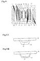
- Fig. 1 is a magnified plan view of a semiconductor element mounting die pad 14 according to the present invention.
- the semiconductor element mounting die pad 14 is supported by the tie bars 16 as mentioned above.
- a plurality of dimples 19 are formed in a pattern on the pad 14.
- the slits 18 extend through the pad 14 from the face to the back side and are in pairs with the slits of each pair separated by width of a dimple 19.
- punching or chemical etching is employed. These methods are the same as the methods for forming the lead frame 11. Therefore, if slits are disposed at the same time as forming the lead frames 11, the process is not complicated. They can be also formed by any suitable prior art process.
- the dimples 19 are formed by pushing the portion of the pad 14 between the slits 18 of each pair in a direction towards the back side of the pad 14 by press means. Thus, the dimples 19 can be formed together simultaneously with slits 18 in one body.
- the slits 18 are formed in the direction of the tie bar 16, but the slits 18 may be also formed at right angles to the tie bar 16. In this case, the dimples 19 are also formed at right angels to the tie bar 16.
- the pairs of slits 18 and dimples 19 form a pattern which is symmetrical about line D-D′. It may be also symmetrical about line E-E′ through the center in the longitudinal direction of the semiconductor element mounting die pad.
- This symmetric forming of the pairs of slits 18 and dimples 19 is intended to uniformly disperse the stress applied on the semiconductor element mounting die pad 4. That is, the manner of application of stress depends on the shape of the semiconductor element 13. In this example, one semiconductor element 13 is put on the semiconductor element mounting die pad 14. An almost uniform stress is applied to one semiconductor element 13.
- the stress is not applied uniformly. If the stress is not applied uniformly on the semiconductor element 13 in this way, a different pattern of slits 18 and dimples 19 is formed depending on the distribution state of the stress. In this case, the pairs of slits 18 and dimples 19 do not always form a symmetrical pattern on the semiconductor element mounting die pad 14.
- the dimple 19 in this embodiment is 0.2 to 1.2 mm in width, 0.4 to 1.5 mm in length, and the width of slit 18 is 0.1 to 0.8 mm.
- the width and length of dimple 19 and width of slit 18 depends on the manufacturing restrictions. When the press technology and etching technology are developed, it is possible to use dimensions which are smaller than the value of these lower limits.
- the dimples 19 and slits 18 can be formed finely, the stress distribution may be controlled more precisely. That is, the pairs of slits 18 and dimple 19 are disposed at the exact positions corresponding to the stress induced in the process of forming the resin mold portion 21. Thus, the stress occurring locally may be dispersed uniformly.
- the upper limit of the width of the dimple 19 varies significantly depending on the area of the semiconductor element mounting die pad 14. As the area of the semiconductor element mounting pad 14 becomes wider, the upper limit may be extended. However, if the upper limit is too large, it is difficult to control the stress, and cracks due to stress concentration are formed.
- the dimples 19 and slits 18 are combined and their area is small, and therefore if the stress distribution is not uniform, as well as when the stress is distributed uniformly in the semiconductor element 13, the stress can be controlled in the narrow region in the semiconductor element 13, and it does not matter if the resin mold portion is further reduced in thickness.
- Fig. 2 is a cross section on line D-D′ of the resin sealed semiconductor device of the invention shown in fig. 1.
- This sectional view is a section along the longitudinal direction of three pairs of slits 18 forming three dimples 19.
- the view clearly shows a cavity 22 formed as a result of the clearance between the bottom line F of the semiconductor element mounting die pad 14 and the top line G of the bottom of the dimple 19.
- the resin pours into the dimples 19 to bond the semiconductor element 13 and semiconductor element mounting die pad 14 firmly.
- the size of the cavity 22 is sufficient for the resin of the resin mold portion 21 to pour into the dimples 19 and penetrate through it.
- the resin is injected around the dimples 19 for sealing.
- the semiconductor element mounting die pad 14 is bonded firmly to the resin mold portion 21. It helps eliminate corrosion of wiring metal due to impurities contained in the resin mold portion 21. At the same time, it results in there being sufficient mechanical strength to prevent breakdown of the resin mold portion 21.
- the semiconductor element 13 is bonded by synthetic resin adhesive is used, but similarly it is also possible to bond using tin-lead solder or silicone resin.
- soldering forms a similar film to that made by plating. Therefore the solder does into the dimples 19 thereby plugging them.
- the dimples 19 is covered by solder, it forms a so-called deformed dimple structure. In this case, as compared with this embodiment, the adhesion strength of the semiconductor element mounting die pad 14 and semiconductor element 13 becomes lower.
- the bonding pads formed on the semiconductor element 13 is wire-bonded to the leads 15 by fine metal wires 20. Afterward, in the region indicated by dotted line in Fig. 2, the resin mold portion 21 is formed.
- any excess resin (the resin patch) formed on or between the leads 15 between the inside of the dam bar 17 and the wall of the resin mold portion 21 is removed. Thereafter, the dam bar 17 portions between leads 15 are cut off and the outer front end portion of the lead 15 is also severed at the desired portion and the leads 15 are formed into specified shape. The tie bars 16 are also severed. By this process, a resin sealed semiconductor device is completed.
- Fig. 4 shows a plan view of the lead frame for explaining the formation of the resin patch.
- the entire structure is same as explained in fig. 3 and the same reference numerals refer to the same parts.
- the dam bar 17 prevents the resin from flowing out sideways beyond the dam bar 17.
- the injected resin flows toward the dam bar 17, and the resin solidifies to form a resin patch (also known as thick burr). Since the material in the region H will be plated in a subsequent process, this resin patch has to be removed e.g. by being punched out. Thereafter, the dam bar 17 portions between the leads 15 are cut off as are the outer front end portions of the leads 15. The outer front end portion is region I in the diagram.
- the leads 15 may be formed into a specified shape.
- the resin for sealing fills up the inside of the dimples 19 from the cavity 22 in the dimples 19. At this time, the resin also contacts the rear side of the semiconductor element 13 overlying the dimples 19. In this way, the semiconductor element mounting die pad 14 is firmly bonded to the resin mold portion 21.
- the coefficient of thermal expansion differs between the semiconductor element mounting die pad 14 and the resin mold portion 21. Accordingly, by quick heating or quick cooling, a stress occurs for the differential portion of the coefficient of thermal expansion. In this embodiment, however, since the slits 18 and dimples 19 are formed in the semiconductor element mounting die pad 14, the stress is dispersed and absorbed by the dimples 19, so that formation of cracks in the resin due to stress may be prevented.
- the resin sealed semiconductor device in this embodiment was suddenly heated at the temperature of about 260 degrees, and it was found that the resin mold portion 21 and the semiconductor element mounting die pad 14 did not separate. Further, if heated and cooled quickly in a temperature range of -65 degrees to 150 degrees, it was confirmed that cracks were not caused in the resin mold portion 21.
- the slits 18 are parallel and the dimples 19 are formed linearly, but the dimples 19 may be also formed in square, star-shape, rhombic form, triangle, circle or their deformations, that is, the side portions may be formed in slits while leaving corners or other parts.
- Linear dimples 19 are suited to a rectangular semiconductor element 13.
- a square semiconductor element is deformed with a greater force than a rectangular semiconductor element. That is, the rectangular shape is more likely to be deformed by the stress of distortion.
- the shape of a dimple 19 is symmetrical about a point, the stress may be applied uniformly. That is, a uniform stress distribution is realized when the shape of the dimple 19 is symmetrical about a point, such as square, star-shape, rhombus, triangle, circle or their deformations.
- Fig. 5 shows magnified side views of the peripheral part of a dimple 19 formed by chemical etching or other method.
- Fig. 5 (a) is a magnified view of the dimple 19 without half etching
- Fig. 5 (b) is magnified view after half etching.
- the dimple 19 from the side clearly shows the cavity 22.
- the size of this cavity 22 is different.
- the wall thickness of the dimple 19 is reduced. Accordingly, the area of the cavity 22 is substantially increased.
- the resin used in the resin mold portion 21 is free to flow into the cavity 22 of the dimple 19, and the semiconductor element 13 and semiconductor element mounting die pad 14 are bonded firmly.
- the size of the cavity 22 may be increased, and the resin of the resin mold portion 21 is free to pour and penetrate into the dimple 19.
- an allowance is given to the material strength of the resin.
- the semiconductor element mounting die pad 14 is firmly bonded with the resin mold portion 21.
- corrosion of wiring metal by the impurities contained in the sealing resin may be eliminated.
- the mechanical strength is sufficient to prevent breakdown of the resin mold portion 21.
- the stress can be controlled in the narrow region in the semiconductor element 13.
Landscapes
- Lead Frames For Integrated Circuits (AREA)
- Structures Or Materials For Encapsulating Or Coating Semiconductor Devices Or Solid State Devices (AREA)
Applications Claiming Priority (2)
| Application Number | Priority Date | Filing Date | Title |
|---|---|---|---|
| JP18168/91 | 1991-02-12 | ||
| JP1816891 | 1991-02-12 |
Publications (2)
| Publication Number | Publication Date |
|---|---|
| EP0503769A1 true EP0503769A1 (de) | 1992-09-16 |
| EP0503769B1 EP0503769B1 (de) | 1998-12-23 |
Family
ID=11964083
Family Applications (1)
| Application Number | Title | Priority Date | Filing Date |
|---|---|---|---|
| EP19920301150 Expired - Lifetime EP0503769B1 (de) | 1991-02-12 | 1992-02-12 | Leiterrahmen und in Harz versiegelte Halbleitervorrichtung dafür |
Country Status (3)
| Country | Link |
|---|---|
| US (1) | US5397915A (de) |
| EP (1) | EP0503769B1 (de) |
| DE (1) | DE69227937T2 (de) |
Cited By (3)
| Publication number | Priority date | Publication date | Assignee | Title |
|---|---|---|---|---|
| GB2336720A (en) * | 1998-04-24 | 1999-10-27 | Sony Corp | Lead frames for semiconductor devices |
| US7755199B2 (en) * | 2001-01-08 | 2010-07-13 | Jiahn-Chang Wu | Flexible lead surface-mount semiconductor package |
| DE10221085B4 (de) * | 2002-05-11 | 2012-07-26 | Robert Bosch Gmbh | Baugruppe mit einer Verbindungseinrichtung zum Kontaktieren eines Halbleiter-Bauelements und Herstellungsverfahren |
Families Citing this family (28)
| Publication number | Priority date | Publication date | Assignee | Title |
|---|---|---|---|---|
| JP3420827B2 (ja) * | 1994-04-28 | 2003-06-30 | ローム株式会社 | 半導体集積回路装置の製造方法及びリードフレーム |
| JPH0878605A (ja) * | 1994-09-01 | 1996-03-22 | Hitachi Ltd | リードフレームおよびそれを用いた半導体集積回路装置 |
| US5682673A (en) * | 1995-04-17 | 1997-11-04 | Ipac, Inc. | Method for forming encapsulated IC packages |
| JPH0992776A (ja) * | 1995-09-28 | 1997-04-04 | Mitsubishi Electric Corp | リードフレームおよび半導体装置 |
| JPH09153586A (ja) * | 1995-12-01 | 1997-06-10 | Texas Instr Japan Ltd | 半導体装置、その製造方法、及びリードフレーム |
| US5902959A (en) * | 1996-09-05 | 1999-05-11 | International Rectifier Corporation | Lead frame with waffled front and rear surfaces |
| JP2000058735A (ja) * | 1998-08-07 | 2000-02-25 | Hitachi Ltd | リードフレーム、半導体装置及び半導体装置の製造方法 |
| JP3602997B2 (ja) * | 1999-12-15 | 2004-12-15 | 松下電器産業株式会社 | 半導体装置及び半導体装置の製造方法 |
| JP3420153B2 (ja) * | 2000-01-24 | 2003-06-23 | Necエレクトロニクス株式会社 | 半導体装置及びその製造方法 |
| US6306684B1 (en) | 2000-03-16 | 2001-10-23 | Microchip Technology Incorporated | Stress reducing lead-frame for plastic encapsulation |
| US6544817B2 (en) * | 2000-06-23 | 2003-04-08 | Carsem Semiconductor Sdn. Bhd. | Method for sawing a moulded leadframe package |
| US7034382B2 (en) * | 2001-04-16 | 2006-04-25 | M/A-Com, Inc. | Leadframe-based chip scale package |
| US7122884B2 (en) * | 2002-04-16 | 2006-10-17 | Fairchild Semiconductor Corporation | Robust leaded molded packages and methods for forming the same |
| JP3867639B2 (ja) * | 2002-07-31 | 2007-01-10 | 株式会社デンソー | 混成集積回路装置 |
| US20040084508A1 (en) * | 2002-10-30 | 2004-05-06 | Advanpack Solutions Pte. Ltd. | Method for constraining the spread of solder during reflow for preplated high wettability lead frame flip chip assembly |
| JP2004179253A (ja) * | 2002-11-25 | 2004-06-24 | Nec Semiconductors Kyushu Ltd | 半導体装置およびその製造方法 |
| US6867481B2 (en) * | 2003-04-11 | 2005-03-15 | Fairchild Semiconductor Corporation | Lead frame structure with aperture or groove for flip chip in a leaded molded package |
| US6921967B2 (en) * | 2003-09-24 | 2005-07-26 | Amkor Technology, Inc. | Reinforced die pad support structure |
| US20070176271A1 (en) * | 2006-02-01 | 2007-08-02 | Stats Chippac Ltd. | Integrated circuit package system having die-attach pad with elevated bondline thickness |
| EP1983567B1 (de) * | 2006-02-03 | 2018-08-15 | Mtex Matsumura Corporation | Aus harz hergestellte hohle kapselung und herstellungsverfahren dafür |
| TWI305407B (en) * | 2006-05-22 | 2009-01-11 | Advanced Semiconductor Eng | Package structure and lead frame using the same |
| DE102006045415A1 (de) * | 2006-09-26 | 2008-04-03 | Infineon Technologies Ag | Bauelementanordnung mit einem Träger |
| JP2008085002A (ja) * | 2006-09-27 | 2008-04-10 | Sanyo Electric Co Ltd | 半導体装置およびその製造方法 |
| JP4757790B2 (ja) * | 2006-12-22 | 2011-08-24 | 富士通コンポーネント株式会社 | 半導体素子の実装構造及びプリント回路基板 |
| US8274162B2 (en) * | 2007-01-20 | 2012-09-25 | Triquint Semiconductor, Inc. | Apparatus and method for reduced delamination of an integrated circuit module |
| US7808089B2 (en) * | 2007-12-18 | 2010-10-05 | National Semiconductor Corporation | Leadframe having die attach pad with delamination and crack-arresting features |
| US20090152683A1 (en) * | 2007-12-18 | 2009-06-18 | National Semiconductor Corporation | Rounded die configuration for stress minimization and enhanced thermo-mechanical reliability |
| US8836104B2 (en) * | 2012-03-03 | 2014-09-16 | Ho-Yuan Yu | Apparatus for chip thermal stress relief |
Citations (1)
| Publication number | Priority date | Publication date | Assignee | Title |
|---|---|---|---|---|
| EP0345760A2 (de) * | 1988-06-08 | 1989-12-13 | STMicroelectronics S.r.l. | Halbleiterbauelement in Kunststoffgehäuse mit Mittel, um die Chipsträgerscheibe im Kunststoffkörper zu verankern |
Family Cites Families (10)
| Publication number | Priority date | Publication date | Assignee | Title |
|---|---|---|---|---|
| JPS58207645A (ja) * | 1982-05-28 | 1983-12-03 | Fujitsu Ltd | 半導体装置 |
| US5126820A (en) * | 1985-02-01 | 1992-06-30 | Advanced Micro Devices, Inc. | Thermal expansion compensated metal lead frame for integrated circuit package |
| JPS62268151A (ja) * | 1986-05-16 | 1987-11-20 | Hitachi Ltd | 集積回路用リ−ドフレ−ム |
| US4884124A (en) * | 1986-08-19 | 1989-11-28 | Mitsubishi Denki Kabushiki Kaisha | Resin-encapsulated semiconductor device |
| JPS6482554A (en) * | 1987-09-24 | 1989-03-28 | Mitsubishi Electric Corp | Resin-sealed semiconductor device |
| JPH01251748A (ja) * | 1988-03-31 | 1989-10-06 | Toppan Printing Co Ltd | 半導体装置用リードフレーム |
| JPH0732215B2 (ja) * | 1988-10-25 | 1995-04-10 | 三菱電機株式会社 | 半導体装置 |
| JPH0777257B2 (ja) * | 1988-11-04 | 1995-08-16 | 日本電気株式会社 | リードフレーム |
| JPH02292850A (ja) * | 1989-05-06 | 1990-12-04 | Matsushita Electron Corp | リードフレーム |
| US5175610A (en) * | 1990-05-09 | 1992-12-29 | Kabushiki Kaisha Toshiba | Resin molded type semiconductor device having a metallic plate support |
-
1992
- 1992-02-12 US US07/834,466 patent/US5397915A/en not_active Expired - Lifetime
- 1992-02-12 DE DE69227937T patent/DE69227937T2/de not_active Expired - Fee Related
- 1992-02-12 EP EP19920301150 patent/EP0503769B1/de not_active Expired - Lifetime
Patent Citations (1)
| Publication number | Priority date | Publication date | Assignee | Title |
|---|---|---|---|---|
| EP0345760A2 (de) * | 1988-06-08 | 1989-12-13 | STMicroelectronics S.r.l. | Halbleiterbauelement in Kunststoffgehäuse mit Mittel, um die Chipsträgerscheibe im Kunststoffkörper zu verankern |
Non-Patent Citations (3)
| Title |
|---|
| PATENT ABSTRACTS OF JAPAN vol. 012, no. 153 (E-607)11 May 1988 & JP-A-62 268 151 ( HITACHI LTD. ) 20 November 1987 * |
| PATENT ABSTRACTS OF JAPAN vol. 013, no. 307 (E-787)13 July 1989 & JP-A-01 082 554 ( MITSUBISHI ELECTRIC CORP. ) 28 March 1989 * |
| PATENT ABSTRACTS OF JAPAN vol. 015, no. 070 (E-1035)19 February 1991 & JP-A-02 292 850 ( MATSUSHITA ELECTRON CORP ) 4 December 1990 * |
Cited By (4)
| Publication number | Priority date | Publication date | Assignee | Title |
|---|---|---|---|---|
| GB2336720A (en) * | 1998-04-24 | 1999-10-27 | Sony Corp | Lead frames for semiconductor devices |
| US6137160A (en) * | 1998-04-24 | 2000-10-24 | Sony Corporation | Lead frame for semiconductor devices |
| US7755199B2 (en) * | 2001-01-08 | 2010-07-13 | Jiahn-Chang Wu | Flexible lead surface-mount semiconductor package |
| DE10221085B4 (de) * | 2002-05-11 | 2012-07-26 | Robert Bosch Gmbh | Baugruppe mit einer Verbindungseinrichtung zum Kontaktieren eines Halbleiter-Bauelements und Herstellungsverfahren |
Also Published As
| Publication number | Publication date |
|---|---|
| DE69227937D1 (de) | 1999-02-04 |
| EP0503769B1 (de) | 1998-12-23 |
| DE69227937T2 (de) | 1999-05-12 |
| US5397915A (en) | 1995-03-14 |
Similar Documents
| Publication | Publication Date | Title |
|---|---|---|
| EP0503769B1 (de) | Leiterrahmen und in Harz versiegelte Halbleitervorrichtung dafür | |
| US10490486B2 (en) | Semiconductor device | |
| KR100294719B1 (ko) | 수지밀봉형 반도체장치 및 그 제조방법, 리드프레임 | |
| US4984059A (en) | Semiconductor device and a method for fabricating the same | |
| US4987474A (en) | Semiconductor device and method of manufacturing the same | |
| US6911353B2 (en) | Semiconductor device and method of manufacturing same | |
| JP2002076228A (ja) | 樹脂封止型半導体装置 | |
| JP2008211041A (ja) | 半導体装置、リードフレームおよび半導体装置の製造方法 | |
| US20090212404A1 (en) | Leadframe having mold lock vent | |
| JP2000294715A (ja) | 半導体装置及び半導体装置の製造方法 | |
| US6501160B1 (en) | Semiconductor device and a method of manufacturing the same and a mount structure | |
| JP2915282B2 (ja) | プラスチックモールドした集積回路パッケージ | |
| JP2936769B2 (ja) | 半導体装置用リードフレーム | |
| JP3040235B2 (ja) | リードフレームとそれを用いた樹脂封止型半導体装置 | |
| EP0474224B1 (de) | Halbleiteranordnung mit mehreren Halbleiterchips | |
| JPS61237458A (ja) | 樹脂封止型半導体装置 | |
| KR100391124B1 (ko) | 반도체 패키지의 베이스, 이를 이용한 반도체 패키지 및그 제조방법 | |
| JP3211116B2 (ja) | 電子部品及びそのモジュール構造 | |
| JPS6336699Y2 (de) | ||
| JPH0463543B2 (de) | ||
| KR0119759Y1 (ko) | 버텀 리드형 반도체 패키지 | |
| JPH03138952A (ja) | 半導体デバイス | |
| JPH0758246A (ja) | 半導体装置とその製造方法 | |
| JPH0722571A (ja) | 樹脂封止型半導体装置 | |
| JPH10125851A (ja) | 半導体装置およびその製造方法並びにそれに使用されるリードフレーム |
Legal Events
| Date | Code | Title | Description |
|---|---|---|---|
| PUAI | Public reference made under article 153(3) epc to a published international application that has entered the european phase |
Free format text: ORIGINAL CODE: 0009012 |
|
| AK | Designated contracting states |
Kind code of ref document: A1 Designated state(s): DE FR GB |
|
| 17P | Request for examination filed |
Effective date: 19921030 |
|
| 17Q | First examination report despatched |
Effective date: 19950125 |
|
| GRAG | Despatch of communication of intention to grant |
Free format text: ORIGINAL CODE: EPIDOS AGRA |
|
| GRAG | Despatch of communication of intention to grant |
Free format text: ORIGINAL CODE: EPIDOS AGRA |
|
| GRAH | Despatch of communication of intention to grant a patent |
Free format text: ORIGINAL CODE: EPIDOS IGRA |
|
| GRAH | Despatch of communication of intention to grant a patent |
Free format text: ORIGINAL CODE: EPIDOS IGRA |
|
| GRAA | (expected) grant |
Free format text: ORIGINAL CODE: 0009210 |
|
| AK | Designated contracting states |
Kind code of ref document: B1 Designated state(s): DE FR GB |
|
| REF | Corresponds to: |
Ref document number: 69227937 Country of ref document: DE Date of ref document: 19990204 |
|
| ET | Fr: translation filed | ||
| PLBE | No opposition filed within time limit |
Free format text: ORIGINAL CODE: 0009261 |
|
| 26N | No opposition filed | ||
| REG | Reference to a national code |
Ref country code: GB Ref legal event code: IF02 |
|
| REG | Reference to a national code |
Ref country code: GB Ref legal event code: 732E |
|
| PGFP | Annual fee paid to national office [announced via postgrant information from national office to epo] |
Ref country code: FR Payment date: 20030210 Year of fee payment: 12 |
|
| PGFP | Annual fee paid to national office [announced via postgrant information from national office to epo] |
Ref country code: DE Payment date: 20030220 Year of fee payment: 12 |
|
| REG | Reference to a national code |
Ref country code: FR Ref legal event code: TP |
|
| PG25 | Lapsed in a contracting state [announced via postgrant information from national office to epo] |
Ref country code: DE Free format text: LAPSE BECAUSE OF NON-PAYMENT OF DUE FEES Effective date: 20040901 |
|
| PG25 | Lapsed in a contracting state [announced via postgrant information from national office to epo] |
Ref country code: FR Free format text: LAPSE BECAUSE OF NON-PAYMENT OF DUE FEES Effective date: 20041029 |
|
| REG | Reference to a national code |
Ref country code: FR Ref legal event code: ST |
|
| REG | Reference to a national code |
Ref country code: GB Ref legal event code: 746 Effective date: 20091215 |
|
| PGFP | Annual fee paid to national office [announced via postgrant information from national office to epo] |
Ref country code: GB Payment date: 20110209 Year of fee payment: 20 |
|
| REG | Reference to a national code |
Ref country code: GB Ref legal event code: PE20 Expiry date: 20120211 |
|
| PG25 | Lapsed in a contracting state [announced via postgrant information from national office to epo] |
Ref country code: GB Free format text: LAPSE BECAUSE OF EXPIRATION OF PROTECTION Effective date: 20120211 |