EP0345760A2 - Halbleiterbauelement in Kunststoffgehäuse mit Mittel, um die Chipsträgerscheibe im Kunststoffkörper zu verankern - Google Patents
Halbleiterbauelement in Kunststoffgehäuse mit Mittel, um die Chipsträgerscheibe im Kunststoffkörper zu verankern Download PDFInfo
- Publication number
- EP0345760A2 EP0345760A2 EP89110302A EP89110302A EP0345760A2 EP 0345760 A2 EP0345760 A2 EP 0345760A2 EP 89110302 A EP89110302 A EP 89110302A EP 89110302 A EP89110302 A EP 89110302A EP 0345760 A2 EP0345760 A2 EP 0345760A2
- Authority
- EP
- European Patent Office
- Prior art keywords
- slice
- chip
- plastic
- semiconductor device
- carrying
- Prior art date
- Legal status (The legal status is an assumption and is not a legal conclusion. Google has not performed a legal analysis and makes no representation as to the accuracy of the status listed.)
- Withdrawn
Links
Images

Classifications
-
- H—ELECTRICITY
- H10—SEMICONDUCTOR DEVICES; ELECTRIC SOLID-STATE DEVICES NOT OTHERWISE PROVIDED FOR
- H10W—GENERIC PACKAGES, INTERCONNECTIONS, CONNECTORS OR OTHER CONSTRUCTIONAL DETAILS OF DEVICES COVERED BY CLASS H10
- H10W70/00—Package substrates; Interposers; Redistribution layers [RDL]
- H10W70/40—Leadframes
- H10W70/411—Chip-supporting parts, e.g. die pads
-
- H—ELECTRICITY
- H10—SEMICONDUCTOR DEVICES; ELECTRIC SOLID-STATE DEVICES NOT OTHERWISE PROVIDED FOR
- H10W—GENERIC PACKAGES, INTERCONNECTIONS, CONNECTORS OR OTHER CONSTRUCTIONAL DETAILS OF DEVICES COVERED BY CLASS H10
- H10W90/00—Package configurations
- H10W90/701—Package configurations characterised by the relative positions of pads or connectors relative to package parts
- H10W90/751—Package configurations characterised by the relative positions of pads or connectors relative to package parts of bond wires
- H10W90/756—Package configurations characterised by the relative positions of pads or connectors relative to package parts of bond wires between a chip and a stacked lead frame, conducting package substrate or heat sink
Definitions
- the present invention relates to semiconductor devices and, more particularly, to plastic cases for integrated circuits adapted for "surface mounting".
- a case of plastic comprises a carrying slice for a chip made of semiconductor material, usually silicon, which constitutes the active element of the device, a multiplicity of rigid electrical conductors electrically connected to predetermined areas of the chip by means of thin metal wires and a body of plastic, usually epoxy resin, which embodies the whole with the exception of the terminal ends of the rigid conductors constituting the legs of the device.
- the carrying slice and the electrical conductors are usually obtained by shearing out a single strip of sheet metal.
- the legs are folded in such a way that their end portions are located in the same plane, substantially coincident with the plane of one of the main surfaces of the body of plastic.
- the devices are bonded to the metal tracks of a printed circuit board via a process using a relatively high temperature, typically 200 - 250° C, and of relatively long duration (some tens of seconds). It has been discovered that said process produces within the plastic body phenomena that modify the physical characteristics of the materials and the mechanical stability of the case. In particular, when the ratio of the thickness of the plastic body to the surface of the metal slice of the carrier, determined by the dimensions of the chip, is small, such modifications can cause the case to break.
- the invention has for its object the provision of a semiconductor device in a case of the type described above, which is more resistant to degenerative effects due to the bonding process and which requires no costly modifications of the manufacturing process.
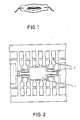
- the carrying slice 1 in Fig. 3 constitutes the central part, modified in accordance with the invention, of a frame structure of the type shown in Fig. 2.
- the slice 1 has a quadrangular part 2 sheared out along two opposing sides and depressed. Advantageously, the formation of the depressed part 2 occurs concurrently with the shearing out of the strip of sheet metal necessary for producing the frame.
- the successive steps for manufacturing the device are usually those taken for this type of cases.
- they include the bonding of a silicon chip 3 made such as to form an integrated circuit on the carrying slice 1, the bonding of thin wires 4 to the conductors 5 of the frame and to appropriate areas 6 of the chip 3 constituting the electrical terminals of the integrated circuit, the formation of an encapsulating body of plastic (not shown) by pressure-injection of a thermosetting epoxy resin in a suitable mold and the shearing out of the portions 7 of sheet metal (Fig. 2) interconnecting the conductors of one frame and the adjacent frames.
- the depressed part 2 forms a kind of eyelet or channel 8 through which the resin can flow during the pressure-injection process.
- the resin left in the channel ensures a solid anchoring of the slice to the body of the case, as a result of which the pressure of the water vapor in any cavity between the resin and the slice during the bonding of the device to a printed circuit board can act practically only beneath the edges of the slice, thereby to a large extent preventing the case from breaking.
- the device according to the invention is particularly advantageous in that it requires no modifications of the manufacturing process, but only a small modification of the equipment for shearing out the strip of sheet metal.
- said equipment in order to produce the device in accordance with the above described embodiment, said equipment comprises a punch designed to shear out partially one part of the slice and to depress the same so as to form the eyelet or channel 8.
Landscapes
- Structures Or Materials For Encapsulating Or Coating Semiconductor Devices Or Solid State Devices (AREA)
- Encapsulation Of And Coatings For Semiconductor Or Solid State Devices (AREA)
Applications Claiming Priority (2)
| Application Number | Priority Date | Filing Date | Title |
|---|---|---|---|
| IT2088588 | 1988-06-08 | ||
| IT20885/88A IT1217802B (it) | 1988-06-08 | 1988-06-08 | Dispositivo a semiconduttore in contenitore in plastica con mezzo du abcioraggio tra lastrina porta "chip" e corpo in plastic |
Publications (2)
| Publication Number | Publication Date |
|---|---|
| EP0345760A2 true EP0345760A2 (de) | 1989-12-13 |
| EP0345760A3 EP0345760A3 (de) | 1990-11-14 |
Family
ID=11173549
Family Applications (1)
| Application Number | Title | Priority Date | Filing Date |
|---|---|---|---|
| EP19890110302 Withdrawn EP0345760A3 (de) | 1988-06-08 | 1989-06-07 | Halbleiterbauelement in Kunststoffgehäuse mit Mittel, um die Chipsträgerscheibe im Kunststoffkörper zu verankern |
Country Status (2)
| Country | Link |
|---|---|
| EP (1) | EP0345760A3 (de) |
| IT (1) | IT1217802B (de) |
Cited By (5)
| Publication number | Priority date | Publication date | Assignee | Title |
|---|---|---|---|---|
| EP0403080A3 (de) * | 1989-06-10 | 1991-12-04 | Gec-Marconi Limited | Verbindungsgeräte |
| EP0503769A1 (de) * | 1991-02-12 | 1992-09-16 | Matsushita Electronics Corporation | Leiterrahmen und in Harz versiegelte Halbleitervorrichtung dafür |
| WO1998013868A1 (de) * | 1996-09-24 | 1998-04-02 | Siemens Aktiengesellschaft | Zuleitungsrahmen für ein mikroelektronisches bauelement |
| GB2320612A (en) * | 1996-12-20 | 1998-06-24 | Motorola Inc | Encapsulating a component mounted on a substrate |
| GB2336720A (en) * | 1998-04-24 | 1999-10-27 | Sony Corp | Lead frames for semiconductor devices |
Family Cites Families (6)
| Publication number | Priority date | Publication date | Assignee | Title |
|---|---|---|---|---|
| US3902189A (en) * | 1974-04-10 | 1975-08-26 | Hunt Electronics | Prefabricated article and methods of maintaining the orientation of parts being bonded thereto |
| JPS56104459A (en) * | 1980-01-25 | 1981-08-20 | Hitachi Ltd | Semiconductor device |
| JPS5916357A (ja) * | 1982-07-19 | 1984-01-27 | Nec Corp | 半導体装置 |
| JPS61185955A (ja) * | 1985-02-13 | 1986-08-19 | Toshiba Corp | 半導体装置 |
| JPS62200751A (ja) * | 1986-02-28 | 1987-09-04 | Dainippon Printing Co Ltd | 半導体装置用リ−ドフレ−ム |
| JPS62268151A (ja) * | 1986-05-16 | 1987-11-20 | Hitachi Ltd | 集積回路用リ−ドフレ−ム |
-
1988
- 1988-06-08 IT IT20885/88A patent/IT1217802B/it active
-
1989
- 1989-06-07 EP EP19890110302 patent/EP0345760A3/de not_active Withdrawn
Cited By (6)
| Publication number | Priority date | Publication date | Assignee | Title |
|---|---|---|---|---|
| EP0403080A3 (de) * | 1989-06-10 | 1991-12-04 | Gec-Marconi Limited | Verbindungsgeräte |
| EP0503769A1 (de) * | 1991-02-12 | 1992-09-16 | Matsushita Electronics Corporation | Leiterrahmen und in Harz versiegelte Halbleitervorrichtung dafür |
| WO1998013868A1 (de) * | 1996-09-24 | 1998-04-02 | Siemens Aktiengesellschaft | Zuleitungsrahmen für ein mikroelektronisches bauelement |
| GB2320612A (en) * | 1996-12-20 | 1998-06-24 | Motorola Inc | Encapsulating a component mounted on a substrate |
| GB2336720A (en) * | 1998-04-24 | 1999-10-27 | Sony Corp | Lead frames for semiconductor devices |
| US6137160A (en) * | 1998-04-24 | 2000-10-24 | Sony Corporation | Lead frame for semiconductor devices |
Also Published As
| Publication number | Publication date |
|---|---|
| IT8820885A0 (it) | 1988-06-08 |
| IT1217802B (it) | 1990-03-30 |
| EP0345760A3 (de) | 1990-11-14 |
Similar Documents
| Publication | Publication Date | Title |
|---|---|---|
| US5973388A (en) | Leadframe, method of manufacturing a leadframe, and method of packaging an electronic component utilizing the leadframe | |
| US4942454A (en) | Resin sealed semiconductor device | |
| KR930014920A (ko) | 반도체 장치 어셈블리 | |
| KR950025961A (ko) | 반도체장치 및 그 제조방법 | |
| KR960019684A (ko) | 리드프레임과 그 제조방법 | |
| EP0544915A4 (en) | Package structure of semiconductor device and manufacturing method therefor | |
| US20010035566A1 (en) | Semiconductor device and process for producing the same | |
| KR100231086B1 (ko) | 관통 슬릿이 형성된 다이패드를 포함하는 반도체 칩 패키지 | |
| KR0156622B1 (ko) | 반도체 패키지,리드프레임 및 제조방법 | |
| EP0345760A2 (de) | Halbleiterbauelement in Kunststoffgehäuse mit Mittel, um die Chipsträgerscheibe im Kunststoffkörper zu verankern | |
| KR900019205A (ko) | 반도체장치 및 그 제조방법 | |
| JP3424526B2 (ja) | 電子部品の実装方法 | |
| EP0548496B1 (de) | Form und Verfahren zur Herstellung von Kunststoffpackungen für integrierte Schaltungen die eine freie metallische Wärmesenke enthalten zur Inspektion der Lötverbindung | |
| JPH0715918B2 (ja) | 半導体チップ実装用リード構造体 | |
| US6441480B1 (en) | Microelectronic circuit package | |
| JPH02172266A (ja) | リード、パッケージ及び電気回路装置 | |
| US6605864B2 (en) | Support matrix for integrated semiconductors, and method for producing it | |
| US6153518A (en) | Method of making chip size package substrate | |
| JPS6387730A (ja) | 電子部品の実装構造 | |
| JP3409465B2 (ja) | 樹脂封止型半導体装置 | |
| JP3128955B2 (ja) | 半導体装置及びその製造方法 | |
| KR100388297B1 (ko) | 반도체패키지용 회로기판의 솔더마스크 라미네이션 방법 | |
| JP2959144B2 (ja) | リードフレームの製造方法 | |
| JP3680398B2 (ja) | プリント配線板 | |
| JP3925280B2 (ja) | 半導体装置の製造方法 |
Legal Events
| Date | Code | Title | Description |
|---|---|---|---|
| PUAI | Public reference made under article 153(3) epc to a published international application that has entered the european phase |
Free format text: ORIGINAL CODE: 0009012 |
|
| AK | Designated contracting states |
Kind code of ref document: A2 Designated state(s): DE FR GB NL SE |
|
| PUAL | Search report despatched |
Free format text: ORIGINAL CODE: 0009013 |
|
| RHK1 | Main classification (correction) |
Ipc: H01L 23/495 |
|
| AK | Designated contracting states |
Kind code of ref document: A3 Designated state(s): DE FR GB NL SE |
|
| STAA | Information on the status of an ep patent application or granted ep patent |
Free format text: STATUS: THE APPLICATION IS DEEMED TO BE WITHDRAWN |
|
| 18D | Application deemed to be withdrawn |
Effective date: 19910515 |