EP0345760A2 - Semiconductor device in plastic case with means of anchoring between chip-bearing slice and plastic body - Google Patents
Semiconductor device in plastic case with means of anchoring between chip-bearing slice and plastic body Download PDFInfo
- Publication number
- EP0345760A2 EP0345760A2 EP89110302A EP89110302A EP0345760A2 EP 0345760 A2 EP0345760 A2 EP 0345760A2 EP 89110302 A EP89110302 A EP 89110302A EP 89110302 A EP89110302 A EP 89110302A EP 0345760 A2 EP0345760 A2 EP 0345760A2
- Authority
- EP
- European Patent Office
- Prior art keywords
- slice
- chip
- plastic
- semiconductor device
- carrying
- Prior art date
- Legal status (The legal status is an assumption and is not a legal conclusion. Google has not performed a legal analysis and makes no representation as to the accuracy of the status listed.)
- Withdrawn
Links
- 239000004033 plastic Substances 0.000 title claims abstract description 17
- 239000004065 semiconductor Substances 0.000 title claims abstract description 11
- 238000004873 anchoring Methods 0.000 title description 2
- 239000002184 metal Substances 0.000 claims abstract description 17
- 230000000994 depressogenic effect Effects 0.000 claims abstract description 11
- 239000004020 conductor Substances 0.000 claims description 8
- 239000000463 material Substances 0.000 claims description 5
- 229920005989 resin Polymers 0.000 abstract description 8
- 239000011347 resin Substances 0.000 abstract description 8
- 238000002347 injection Methods 0.000 abstract description 3
- 239000007924 injection Substances 0.000 abstract description 3
- XLYOFNOQVPJJNP-UHFFFAOYSA-N water Substances O XLYOFNOQVPJJNP-UHFFFAOYSA-N 0.000 description 6
- 238000000034 method Methods 0.000 description 5
- 230000004048 modification Effects 0.000 description 5
- 238000012986 modification Methods 0.000 description 5
- 238000010008 shearing Methods 0.000 description 5
- 238000004519 manufacturing process Methods 0.000 description 3
- XUIMIQQOPSSXEZ-UHFFFAOYSA-N Silicon Chemical compound [Si] XUIMIQQOPSSXEZ-UHFFFAOYSA-N 0.000 description 2
- 230000015572 biosynthetic process Effects 0.000 description 2
- 239000003822 epoxy resin Substances 0.000 description 2
- 229940090044 injection Drugs 0.000 description 2
- 229920000647 polyepoxide Polymers 0.000 description 2
- 229910052710 silicon Inorganic materials 0.000 description 2
- 239000010703 silicon Substances 0.000 description 2
- 238000001179 sorption measurement Methods 0.000 description 2
- 235000002017 Zea mays subsp mays Nutrition 0.000 description 1
- 241000482268 Zea mays subsp. mays Species 0.000 description 1
- 238000011109 contamination Methods 0.000 description 1
- 230000003412 degenerative effect Effects 0.000 description 1
- 230000000694 effects Effects 0.000 description 1
- 230000008030 elimination Effects 0.000 description 1
- 238000003379 elimination reaction Methods 0.000 description 1
- 238000005538 encapsulation Methods 0.000 description 1
- 229920000136 polysorbate Polymers 0.000 description 1
- 239000007787 solid Substances 0.000 description 1
- 229920001187 thermosetting polymer Polymers 0.000 description 1
- 238000011282 treatment Methods 0.000 description 1
Images

Classifications
-
- H—ELECTRICITY
- H01—ELECTRIC ELEMENTS
- H01L—SEMICONDUCTOR DEVICES NOT COVERED BY CLASS H10
- H01L23/00—Details of semiconductor or other solid state devices
- H01L23/48—Arrangements for conducting electric current to or from the solid state body in operation, e.g. leads, terminal arrangements ; Selection of materials therefor
- H01L23/488—Arrangements for conducting electric current to or from the solid state body in operation, e.g. leads, terminal arrangements ; Selection of materials therefor consisting of soldered or bonded constructions
- H01L23/495—Lead-frames or other flat leads
- H01L23/49503—Lead-frames or other flat leads characterised by the die pad
-
- H—ELECTRICITY
- H01—ELECTRIC ELEMENTS
- H01L—SEMICONDUCTOR DEVICES NOT COVERED BY CLASS H10
- H01L2224/00—Indexing scheme for arrangements for connecting or disconnecting semiconductor or solid-state bodies and methods related thereto as covered by H01L24/00
- H01L2224/01—Means for bonding being attached to, or being formed on, the surface to be connected, e.g. chip-to-package, die-attach, "first-level" interconnects; Manufacturing methods related thereto
- H01L2224/42—Wire connectors; Manufacturing methods related thereto
- H01L2224/47—Structure, shape, material or disposition of the wire connectors after the connecting process
- H01L2224/48—Structure, shape, material or disposition of the wire connectors after the connecting process of an individual wire connector
- H01L2224/481—Disposition
- H01L2224/48151—Connecting between a semiconductor or solid-state body and an item not being a semiconductor or solid-state body, e.g. chip-to-substrate, chip-to-passive
- H01L2224/48221—Connecting between a semiconductor or solid-state body and an item not being a semiconductor or solid-state body, e.g. chip-to-substrate, chip-to-passive the body and the item being stacked
- H01L2224/48245—Connecting between a semiconductor or solid-state body and an item not being a semiconductor or solid-state body, e.g. chip-to-substrate, chip-to-passive the body and the item being stacked the item being metallic
- H01L2224/48247—Connecting between a semiconductor or solid-state body and an item not being a semiconductor or solid-state body, e.g. chip-to-substrate, chip-to-passive the body and the item being stacked the item being metallic connecting the wire to a bond pad of the item
Definitions
- the present invention relates to semiconductor devices and, more particularly, to plastic cases for integrated circuits adapted for "surface mounting".
- a case of plastic comprises a carrying slice for a chip made of semiconductor material, usually silicon, which constitutes the active element of the device, a multiplicity of rigid electrical conductors electrically connected to predetermined areas of the chip by means of thin metal wires and a body of plastic, usually epoxy resin, which embodies the whole with the exception of the terminal ends of the rigid conductors constituting the legs of the device.
- the carrying slice and the electrical conductors are usually obtained by shearing out a single strip of sheet metal.
- the legs are folded in such a way that their end portions are located in the same plane, substantially coincident with the plane of one of the main surfaces of the body of plastic.
- the devices are bonded to the metal tracks of a printed circuit board via a process using a relatively high temperature, typically 200 - 250° C, and of relatively long duration (some tens of seconds). It has been discovered that said process produces within the plastic body phenomena that modify the physical characteristics of the materials and the mechanical stability of the case. In particular, when the ratio of the thickness of the plastic body to the surface of the metal slice of the carrier, determined by the dimensions of the chip, is small, such modifications can cause the case to break.
- the invention has for its object the provision of a semiconductor device in a case of the type described above, which is more resistant to degenerative effects due to the bonding process and which requires no costly modifications of the manufacturing process.
- the carrying slice 1 in Fig. 3 constitutes the central part, modified in accordance with the invention, of a frame structure of the type shown in Fig. 2.
- the slice 1 has a quadrangular part 2 sheared out along two opposing sides and depressed. Advantageously, the formation of the depressed part 2 occurs concurrently with the shearing out of the strip of sheet metal necessary for producing the frame.
- the successive steps for manufacturing the device are usually those taken for this type of cases.
- they include the bonding of a silicon chip 3 made such as to form an integrated circuit on the carrying slice 1, the bonding of thin wires 4 to the conductors 5 of the frame and to appropriate areas 6 of the chip 3 constituting the electrical terminals of the integrated circuit, the formation of an encapsulating body of plastic (not shown) by pressure-injection of a thermosetting epoxy resin in a suitable mold and the shearing out of the portions 7 of sheet metal (Fig. 2) interconnecting the conductors of one frame and the adjacent frames.
- the depressed part 2 forms a kind of eyelet or channel 8 through which the resin can flow during the pressure-injection process.
- the resin left in the channel ensures a solid anchoring of the slice to the body of the case, as a result of which the pressure of the water vapor in any cavity between the resin and the slice during the bonding of the device to a printed circuit board can act practically only beneath the edges of the slice, thereby to a large extent preventing the case from breaking.
- the device according to the invention is particularly advantageous in that it requires no modifications of the manufacturing process, but only a small modification of the equipment for shearing out the strip of sheet metal.
- said equipment in order to produce the device in accordance with the above described embodiment, said equipment comprises a punch designed to shear out partially one part of the slice and to depress the same so as to form the eyelet or channel 8.
Abstract
In order to anchor a carrying metal slice (1) of a semiconductor device to a case being formed by pressure-injection of resin, the slice (1), which carries a semiconductor chip (3) comprises at least one part (2) that is depressed in relation to the surface on which the chip (3) is mounted, wherein said depressed part (2) has at least one hole. Plastic of the case extends through the hole to the interior of the volume delimited by the depressed part and by the chip (3) carried by the metal slice (1).
Description
- The present invention relates to semiconductor devices and, more particularly, to plastic cases for integrated circuits adapted for "surface mounting".
- As is well known, a case of plastic comprises a carrying slice for a chip made of semiconductor material, usually silicon, which constitutes the active element of the device, a multiplicity of rigid electrical conductors electrically connected to predetermined areas of the chip by means of thin metal wires and a body of plastic, usually epoxy resin, which embodies the whole with the exception of the terminal ends of the rigid conductors constituting the legs of the device. The carrying slice and the electrical conductors are usually obtained by shearing out a single strip of sheet metal. In the case of devices intended for surface mounting, the legs are folded in such a way that their end portions are located in the same plane, substantially coincident with the plane of one of the main surfaces of the body of plastic.
- For surface mounting, the devices are bonded to the metal tracks of a printed circuit board via a process using a relatively high temperature, typically 200 - 250° C, and of relatively long duration (some tens of seconds). It has been discovered that said process produces within the plastic body phenomena that modify the physical characteristics of the materials and the mechanical stability of the case. In particular, when the ratio of the thickness of the plastic body to the surface of the metal slice of the carrier, determined by the dimensions of the chip, is small, such modifications can cause the case to break.
- The phenomenon, shown in Fig. 1, appears to occur in the following manner:
- water, present in the resin by adsorption from the environment, migrates to both the inner and outer surfaces of the body;
- if the adherence between the plastic body and the parts embodied therein is not perfect or fails because of the different expansions of the materials during the thermal cycle, a cavity may form between the plastic and the chip and between the plastic and the lower surface of the carrying slice, in which water can accumulate;
- due to the elevated temperature, the water evaporates and applies pressure to the walls of the cavity;
- the pressure of the vapor within the body deforms the walls of the case and, in limit cases, causes it to break (it is be noted that the wall that gives way first is the wall which is adjacent to the metal slice and is the thinnest). - In view of the present tendency to make increasingly complex integrated circuits, employing chips of ever greater dimensions but without increasing the dimensions of the cases, it is obvious that the phenomenon described above constitutes a serious problem, since it imposes a limit on the possibility of using certain standard cases.
- In order to overcome the above described destructive effect, which is known to those skilled in the art as "pop corn noise", several expedients have been recommended, such as:
- elimination of the adsorbed water by baking the pieces prior to bonding,
- protection of the pieces during storage so as to avoid adsorption of water,
- improvement of adhesion between the resin and the components of the device within the body by treating, chemically or mechanically, the surface of the carrying slice,
- reduction of the surface of contact between resin and slice, providing a window which passes through the body of resin to the surface of the slice. - All the expedients above mentioned have more or less serious disadvantages. In particular, the first three expedients require costly additional treatments, and the fourth expedient leads to a loss of dependability due to the high risk of contamination of the chip.
- The invention has for its object the provision of a semiconductor device in a case of the type described above, which is more resistant to degenerative effects due to the bonding process and which requires no costly modifications of the manufacturing process.
- This object is achieved by means of a device having the characteristics set forth in the appended claims.
- One embodiment of the invention will be described hereinbelow by way of example, which is not limitative, with reference to the accompanying drawings, in which:
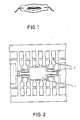
- - Fig. 1 shows a device made of plastic for surface mounting known from the prior art and which is deformed by thermal strains during the bonding process,
- - Fig. 2 shows an enlarged portion of a strip of sheet metal sheared out along a customary pattern and used for producing a device of the type shown in Fig. 1;
- - Fig. 3 is a perspective and enlarged view of a carrying slice of a device according to the invention, and
- - Figs. 4 and 5 are a schematic top plan view and a cross-sectional view, respectively, of a part of the device according to the invention prior to encapsulation in plastic.
- With reference to the drawings, in which like reference numerals denote like or equivalent parts, the
carrying slice 1 in Fig. 3 constitutes the central part, modified in accordance with the invention, of a frame structure of the type shown in Fig. 2. In particular, theslice 1 has aquadrangular part 2 sheared out along two opposing sides and depressed. Advantageously, the formation of thedepressed part 2 occurs concurrently with the shearing out of the strip of sheet metal necessary for producing the frame. - The successive steps for manufacturing the device are usually those taken for this type of cases. In particular, they include the bonding of a
silicon chip 3 made such as to form an integrated circuit on thecarrying slice 1, the bonding of thin wires 4 to theconductors 5 of the frame and toappropriate areas 6 of thechip 3 constituting the electrical terminals of the integrated circuit, the formation of an encapsulating body of plastic (not shown) by pressure-injection of a thermosetting epoxy resin in a suitable mold and the shearing out of theportions 7 of sheet metal (Fig. 2) interconnecting the conductors of one frame and the adjacent frames. As can particularly be seen in Fig. 5, thedepressed part 2 forms a kind of eyelet orchannel 8 through which the resin can flow during the pressure-injection process. Following the hardening, the resin left in the channel ensures a solid anchoring of the slice to the body of the case, as a result of which the pressure of the water vapor in any cavity between the resin and the slice during the bonding of the device to a printed circuit board can act practically only beneath the edges of the slice, thereby to a large extent preventing the case from breaking. - It should also be noted that the device according to the invention is particularly advantageous in that it requires no modifications of the manufacturing process, but only a small modification of the equipment for shearing out the strip of sheet metal. In particular, in order to produce the device in accordance with the above described embodiment, said equipment comprises a punch designed to shear out partially one part of the slice and to depress the same so as to form the eyelet or
channel 8. - While one embodiment of the invention has been shown and described, it is obvious that numerous modifications can be made without departing from the scope of the inventive concept. For example, in the same slice there can be formed more than one depressed part, or the depressed part can have a form other than the quadrangle shown, or it may have one or more holes obtained other than by shearing.
Claims (1)
- A semiconductor device comprising a carrying metal slice (1), a chip (3) of semiconductor material fixed to the carrying slice (1), a multiplicity of metal conductors (5) adjacent to the carrying slice (1), a multiplicity of metal wires (4) which connect predetermined points (6) of the semiconductor chip (3) to the metal conductors (5), and a body of plastic which embodies the whole with the exception of the end portions of the metal conductors (5),
characterized in that
the carrying metal slice (3) has at least one part (2) that is depressed in relation to the surface on which the chip (3) of semiconductor material is mounted, said depressed part (2) having at least one hole, and in that the plastic of the body extends through the hole to the interior of the volume delimited by the depressed part and by the semiconductor chip (3).
Applications Claiming Priority (2)
| Application Number | Priority Date | Filing Date | Title |
|---|---|---|---|
| IT2088588 | 1988-06-08 | ||
| IT20885/88A IT1217802B (en) | 1988-06-08 | 1988-06-08 | SEMICONDUCTOR DEVICE IN PLASTIC CONTAINER WITH HALF DU ABCIORAGGIO BETWEEN "CHIP" DOOR PLATE AND PLASTIC BODY |
Publications (2)
| Publication Number | Publication Date |
|---|---|
| EP0345760A2 true EP0345760A2 (en) | 1989-12-13 |
| EP0345760A3 EP0345760A3 (en) | 1990-11-14 |
Family
ID=11173549
Family Applications (1)
| Application Number | Title | Priority Date | Filing Date |
|---|---|---|---|
| EP19890110302 Withdrawn EP0345760A3 (en) | 1988-06-08 | 1989-06-07 | Semiconductor device in plastic case with means of anchoring between chip-bearing slice and plastic body |
Country Status (2)
| Country | Link |
|---|---|
| EP (1) | EP0345760A3 (en) |
| IT (1) | IT1217802B (en) |
Cited By (5)
| Publication number | Priority date | Publication date | Assignee | Title |
|---|---|---|---|---|
| EP0403080A2 (en) * | 1989-06-10 | 1990-12-19 | Gec-Marconi Limited | Bonding devices |
| EP0503769A1 (en) * | 1991-02-12 | 1992-09-16 | Matsushita Electronics Corporation | Lead frame and resin sealed semiconductor device using the same |
| WO1998013868A1 (en) * | 1996-09-24 | 1998-04-02 | Siemens Aktiengesellschaft | Leadframe for a microelectronic component |
| GB2320612A (en) * | 1996-12-20 | 1998-06-24 | Motorola Inc | Encapsulating a component mounted on a substrate |
| GB2336720A (en) * | 1998-04-24 | 1999-10-27 | Sony Corp | Lead frames for semiconductor devices |
Citations (6)
| Publication number | Priority date | Publication date | Assignee | Title |
|---|---|---|---|---|
| US3902189A (en) * | 1974-04-10 | 1975-08-26 | Hunt Electronics | Prefabricated article and methods of maintaining the orientation of parts being bonded thereto |
| JPS56104459A (en) * | 1980-01-25 | 1981-08-20 | Hitachi Ltd | Semiconductor device |
| JPS5916357A (en) * | 1982-07-19 | 1984-01-27 | Nec Corp | Semiconductor device |
| JPS61185955A (en) * | 1985-02-13 | 1986-08-19 | Toshiba Corp | Semiconductor device |
| JPS62200751A (en) * | 1986-02-28 | 1987-09-04 | Dainippon Printing Co Ltd | Lead frame for semiconductor device |
| JPS62268151A (en) * | 1986-05-16 | 1987-11-20 | Hitachi Ltd | Lead frame for integrated circuit |
-
1988
- 1988-06-08 IT IT20885/88A patent/IT1217802B/en active
-
1989
- 1989-06-07 EP EP19890110302 patent/EP0345760A3/en not_active Withdrawn
Patent Citations (6)
| Publication number | Priority date | Publication date | Assignee | Title |
|---|---|---|---|---|
| US3902189A (en) * | 1974-04-10 | 1975-08-26 | Hunt Electronics | Prefabricated article and methods of maintaining the orientation of parts being bonded thereto |
| JPS56104459A (en) * | 1980-01-25 | 1981-08-20 | Hitachi Ltd | Semiconductor device |
| JPS5916357A (en) * | 1982-07-19 | 1984-01-27 | Nec Corp | Semiconductor device |
| JPS61185955A (en) * | 1985-02-13 | 1986-08-19 | Toshiba Corp | Semiconductor device |
| JPS62200751A (en) * | 1986-02-28 | 1987-09-04 | Dainippon Printing Co Ltd | Lead frame for semiconductor device |
| JPS62268151A (en) * | 1986-05-16 | 1987-11-20 | Hitachi Ltd | Lead frame for integrated circuit |
Non-Patent Citations (5)
| Title |
|---|
| PATENT ABSTRACTS OF JAPAN vol. 11, no. 11 (E-470)(2458) 13 January 1987, & JP-A-61 185955 (TOSHIBA CORP) 19 August 1986, * |
| PATENT ABSTRACTS OF JAPAN vol. 12, no. 153 (E-607)(3000) 11 May 1988, & JP-A-62 268151 (HITACHI) 20 November 1987, * |
| PATENT ABSTRACTS OF JAPAN vol. 12, no. 54 (E-583)(2901) 18 February 1988, & JP-A-62 200751 (DAINIPPON PRINTING CO) 04 September 1987, * |
| PATENT ABSTRACTS OF JAPAN vol. 5, no. 179 (E-82)(851) 17 November 1981, & JP-A-56 104459 (HITACHI SEISAKUSHO) 20 August 1981, * |
| PATENT ABSTRACTS OF JAPAN vol. 8, no. 99 (E-243)(1536) 10 May 1984, & JP-A-59 016357 (NIPPON DENKI) 27 January 1984, * |
Cited By (7)
| Publication number | Priority date | Publication date | Assignee | Title |
|---|---|---|---|---|
| EP0403080A2 (en) * | 1989-06-10 | 1990-12-19 | Gec-Marconi Limited | Bonding devices |
| EP0403080A3 (en) * | 1989-06-10 | 1991-12-04 | Gec-Marconi Limited | Bonding devices |
| EP0503769A1 (en) * | 1991-02-12 | 1992-09-16 | Matsushita Electronics Corporation | Lead frame and resin sealed semiconductor device using the same |
| WO1998013868A1 (en) * | 1996-09-24 | 1998-04-02 | Siemens Aktiengesellschaft | Leadframe for a microelectronic component |
| GB2320612A (en) * | 1996-12-20 | 1998-06-24 | Motorola Inc | Encapsulating a component mounted on a substrate |
| GB2336720A (en) * | 1998-04-24 | 1999-10-27 | Sony Corp | Lead frames for semiconductor devices |
| US6137160A (en) * | 1998-04-24 | 2000-10-24 | Sony Corporation | Lead frame for semiconductor devices |
Also Published As
| Publication number | Publication date |
|---|---|
| IT8820885A0 (en) | 1988-06-08 |
| EP0345760A3 (en) | 1990-11-14 |
| IT1217802B (en) | 1990-03-30 |
Similar Documents
| Publication | Publication Date | Title |
|---|---|---|
| US5973388A (en) | Leadframe, method of manufacturing a leadframe, and method of packaging an electronic component utilizing the leadframe | |
| US4942454A (en) | Resin sealed semiconductor device | |
| US5352851A (en) | Edge-mounted, surface-mount integrated circuit device | |
| US7378731B2 (en) | Heat spreader and package structure utilizing the same | |
| KR930014920A (en) | Semiconductor device assembly | |
| KR970000973B1 (en) | Lead frame and resin-sealed semiconductor device | |
| EP0503769A1 (en) | Lead frame and resin sealed semiconductor device using the same | |
| KR100231086B1 (en) | Semiconductor Chip Package Having Die Pad With Slots Therein | |
| JP2915282B2 (en) | Plastic molded integrated circuit package | |
| EP0345760A2 (en) | Semiconductor device in plastic case with means of anchoring between chip-bearing slice and plastic body | |
| JP3424526B2 (en) | Electronic component mounting method | |
| JPH0715918B2 (en) | Lead structure for semiconductor chip mounting | |
| US6465274B2 (en) | Lead frame tooling design for bleed barrier groove | |
| US6605864B2 (en) | Support matrix for integrated semiconductors, and method for producing it | |
| JP3680398B2 (en) | Printed wiring board | |
| JPS6387730A (en) | Mounting structure of electronic component | |
| JPS6142939A (en) | Chip type semiconductor device | |
| KR19980033656A (en) | Semiconductor package and manufacturing method | |
| JP3925280B2 (en) | Manufacturing method of semiconductor device | |
| KR100388297B1 (en) | solder mask laminating method of circuit board for semiconductor package | |
| JP2959144B2 (en) | Lead frame manufacturing method | |
| EP1170793A2 (en) | Support matrix with a bonding channel for an integrated circuit and manufacturing method thereof | |
| JPH02138766A (en) | Package structure of electronic component | |
| JP3128955B2 (en) | Semiconductor device and manufacturing method thereof | |
| KR100226782B1 (en) | Structure of semiconductor package |
Legal Events
| Date | Code | Title | Description |
|---|---|---|---|
| PUAI | Public reference made under article 153(3) epc to a published international application that has entered the european phase |
Free format text: ORIGINAL CODE: 0009012 |
|
| AK | Designated contracting states |
Kind code of ref document: A2 Designated state(s): DE FR GB NL SE |
|
| PUAL | Search report despatched |
Free format text: ORIGINAL CODE: 0009013 |
|
| RHK1 | Main classification (correction) |
Ipc: H01L 23/495 |
|
| AK | Designated contracting states |
Kind code of ref document: A3 Designated state(s): DE FR GB NL SE |
|
| STAA | Information on the status of an ep patent application or granted ep patent |
Free format text: STATUS: THE APPLICATION IS DEEMED TO BE WITHDRAWN |
|
| 18D | Application deemed to be withdrawn |
Effective date: 19910515 |