EP0503078B1 - Dispositif a semi-conducteurs - Google Patents
Dispositif a semi-conducteurs Download PDFInfo
- Publication number
- EP0503078B1 EP0503078B1 EP91916783A EP91916783A EP0503078B1 EP 0503078 B1 EP0503078 B1 EP 0503078B1 EP 91916783 A EP91916783 A EP 91916783A EP 91916783 A EP91916783 A EP 91916783A EP 0503078 B1 EP0503078 B1 EP 0503078B1
- Authority
- EP
- European Patent Office
- Prior art keywords
- film
- ferroelectric
- electrode
- wiring
- upper electrode
- Prior art date
- Legal status (The legal status is an assumption and is not a legal conclusion. Google has not performed a legal analysis and makes no representation as to the accuracy of the status listed.)
- Expired - Lifetime
Links
Images


Classifications
-
- H—ELECTRICITY
- H10—SEMICONDUCTOR DEVICES; ELECTRIC SOLID-STATE DEVICES NOT OTHERWISE PROVIDED FOR
- H10B—ELECTRONIC MEMORY DEVICES
- H10B69/00—Erasable-and-programmable ROM [EPROM] devices not provided for in groups H10B41/00 - H10B63/00, e.g. ultraviolet erasable-and-programmable ROM [UVEPROM] devices
-
- H—ELECTRICITY
- H10—SEMICONDUCTOR DEVICES; ELECTRIC SOLID-STATE DEVICES NOT OTHERWISE PROVIDED FOR
- H10B—ELECTRONIC MEMORY DEVICES
- H10B53/00—Ferroelectric RAM [FeRAM] devices comprising ferroelectric memory capacitors
Definitions
- the present invention relates to a semiconductor device having a ferroelectric material, such as a ferroelectric capacitor, which can be used as a nonvolatile memory or the like.
- a nonvolatile memory using ferroelectric materials which can reverse its polarization according to the voltage polarities applied thereto, has, in principle, the same writing and reading times. Further, at a quiescent or non-operative state (backup time) the afore-mentioned nonvolatile memory keeps polarization (residual polarization), even if no voltage is applied thereto. Therefore, it has been regarded as an ideal nonvolatile memory.
- a nonvolatile memory cell generally comprises, as shown in Fig. 4, an N-type transistor TR which has a gate electrode G connected to a word line W, a drain electrode D connected to a bit line B and a source electrode S connected to one electrode of a ferroelectric capacitor C. The other electrode of the ferroelectric capacitor C is connected to a plate line P.
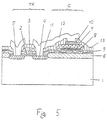
- the semiconductor construction shown in Fig. 5 comprises an N-type MOS transistor TR which has a polysilicon (polycrystal silicon) gate electrode 3 formed through a gate oxide film 2 on a P-type silicon substrate 1.
- Source and drain zones 4 and 5 are N-type high concentration diffusion regions formed in the silicon substrate 1 by using a self-aligning diffusion technique.
- a ferroelectric capacitor C is formed on an interlayer insulation film 7, such as phosphoric glass, etc., disposed between layers on a local oxide film (LOCOS) 6 for isolating elements.
- the ferroelectric capacitor C on the interlayer insulation film 7 is composed of a lower electrode 8 made of platinum (Pt), etc., a ferroelectric film 9 such as PZT, etc. and an upper electrode 10 of gold (Au) or platinum (Pt), stacked in that order.
- the source zone 4 which is a high concentration diffusion region and the upper electrode 10 are connected to each other with a wiring 12 made of Al through a contact hole 11.
- the reference number 13 indicates a second interlayer insulation film made of phosphoric glass and the like.
- Gold (Au) and platinum (Pt), which form the upper electrode 10 are precious metals which do not react with the ferroelectric film and thus achieve a good interface property. Therefore, they are often used as the electrode of a ferroelectric capacitor. Also, because platinum (Pt) has a lattice constant being near that of the ferroelectric material, such as PZT, etc., the effect of improving the crystallization is expected, and as a result, platinum is used more frequently than gold.
- the platinum (Pt) or gold (Au) that is the upper electrode 10 readily reacts with the Al of the wiring electrode 12 at a temperature of around 300°C. Consequently, on carrying out an annealing process and on forming a final protection film (a passivation film) after the formation of the wiring electrode 12, a reaction of the Al of the wiring electrode with the upper electrode 10 reaches to the interface of the upper electrode 10 and the ferroelectric film 9, resulting in a decrease of the residual polarization, i.e. a deterioration of the electrical properties such as a decrease of a signal charge, a decrease of the relative dielectric constant Es, etc.
- the ferroelectric capacitor C is formed by effectively utilizing a space on the local oxide film 6.
- the length of the wiring electrode 12 between the source zone 4 and the upper electrode 10, however, is too prolix, which results in the increase of the memory cell areas.
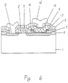
- the present inventor has manufactured for trial a memory cell structure in which, as shown in Fig. 6, the ferroelectric film 9 is directly accumulated over the source zone 4.
- an upper electrode 14 of platinum (Pt) is formed on the ferroelectric film 9, and is connected to a plate line P (not shown) through a wiring electrode 16 of Al.
- the lower electrode 17, made of material such as Pt is formed under the ferroelectric film 9, through a contact hole in an interlayer insulation film 7 of a phosphoric doped glass and the like.
- the object of the present invention is to provide a semiconductor device having a structure in which the formation of the passivation film, the annealing treatment, etc. can be achieved without impeding the function of a nonvolatile memory having a ferroelectric substance therein.
- JP-A-2 288 367 which was published after the priority date of the present patent application, discloses a ferroelectric semiconductor structure in which a ferroelectric layer is formed over a transistor gate, and connected to an impurity layer of the transistor by an underlying electrode formed of a combination of a Ti film and an overlying TiN film.
- the provision of one or more thin, high melting point layers is said to improve reliability and electric characteristics, because the ferroelectric film can be heat treated at a high temperature.
- EP-A-0 448 151 discloses a ferroelectric semiconductor device in which the upper, platinum electrode of a ferroelectric capacitor is connected to the source region of a transistor by metallisation formed of an aluminium conductor layer overlying a diffusion barrier layer formed of an alloy of Titanium and Tungsten, the diffusion barrier layer separating the aluminium from the platinum electrode.
- a formation or structure having a ferroelectric substance on the principal surface or on the inside of a semiconductor body or semiconductor substrate is silicon.
- the present invention is applicable to semiconductor bodies which have a bonding property with oxygen such as compound semiconductors of GaAs, etc.
- Regions of the structure where the ferroelectric substance is formed may be intrinsic semiconductor regions and/or N-type or P-type impurity diffusion regions or zones. Source and drain zones of a MIS-type transistor and diffusion zones for the three electrodes of a bipolar transistor are typical examples of impurity diffusion zones.
- the ferroelectric substance formation can be achieved not only over an active region of an active element, but also over each of the regions of a passive element such as a diffusion resistant layer, a stopper region, etc.
- a ferroelectric capacitor structure can be stacked over an isolation region or the diffusion region. It is also possible to realize the structure having the ferroelectric substance in a trench.
- the present invention takes measures to adopt a construction in which a conductive reaction-preventing film is disposed between an upper electrode and a wiring electrode.
- the present invention adopts a laminated-layers structure in which a lower electrode, a ferroelectric film, an upper electrode, a conductive reaction-preventing film and a wiring electrode are sequentially stacked.
- a ferroelectric substance PbTiO 3 , PZT, (PbTiO 3 , PbZrO 3 ) or PLZT (La, PbTiO 3 , PbZrO 3 ), etc. are generally used.
- These kinds of ferroelectric films are formed by, for example, a sputtering or sol-gel process.
- the electrodes of the ferroelectric film may be formed of, for example, Pt, Pd or Au. It is preferable to use Pt because it has a lattice constant near that of a ferroelectric substance crystal lattice constant.
- the conductive reaction-preventing film may be a metal film having a high melting point such as Mo film, W film, Ti film, etc., a metal silicide film having a high melting point such as MoSi film, TiSi film, etc., a conductive metal nitride film such as TiN film, etc., a conductive metal oxide film such as RuO 2 film, ReO 2 film, etc., a conductive metal nitride oxide film such as TiON film, etc. or a compound film formed of a combination of at least two films selected from these films.
- the structure in which the conductive reaction-preventing film is interposed between the upper electrode and the wiring electrode prevents the reaction of the upper electrode with the wiring electrode, which arises when carrying out the annealing treatment after the formation of the wiring electrode and when forming the final protection film.
- This structure also prevents the diffusion of a wiring electrode material (Al) into the ferroelectric film, and the deterioration of the electric characteristics such as the relative dielectric constant, the amount of polarizing electric charges, etc.
- a ferroelectric memory structure can be realized so that the formation of the passivation film and the annealing treatment can be carried out without impeding the function of a memory having a ferroelectric substrate therein.
- the afore-mentioned conductive reaction-preventing film is used as a wiring electrode. Because the structure has a wiring electrode composed of Al and another wiring electrode composed of the conductive reaction-preventing film independent from each other, it becomes possible to stack the one electrode on the plane surface of the other electrode, which contributes to the high integration of the elements.
- the silicide film comprises a main ingredient of at least any one of the metals selected from the group of Pt, Ru, Re, Mo, Ta and W.
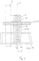
- Fig. 1 is a plan view showing a semiconductor device provided with a ferroelectric capacitor relating to the first embodiment of the present invention
- Fig. 2 is a sectional view showing an A-A' cross-section in the plan view of Fig. 1.
- a semiconductor device is a nonvolatile memory, and its equivalent circuit has a memory cell as shown in Fig. 8.
- a P-type silicon substrate 21 made of a wafer having a specific resistance of, for example, 20 ohm.cm is used.
- structures of an N-type MOS transistor Tr and a ferroelectric capacitor C are formed.
- a semiconductor structure of the N-type MOS transistor Tr comprises a gate electrode 23 made of phosphor-doped polysilicon over a gate insulation film (silicon oxide film) 22 formed on the silicon substrate 21.
- Transistor Tr also has a source region 24 and a drain region 25 which are N-type diffusion regions of a high impurity concentration. The diffusion regions are formed in the substrate by an ion implantation of phosphor under a condition of 80 KV and 5 x 10 15 /cm 2 while using the gate electrode 23 as a mask in a self-aligning manner.
- LOCS local oxide film
- 30 indicates a first interlayer insulation film and, in this embodiment, the structure of the ferroelectric capacitor C is provided on the first interlayer insulation film 30.
- the capacitor C may be called a ferroelectric substance forming structure. This structure has a basic ferroelectric film 29, and an upper electrode 32 and a lower electrode 28 with the ferroelectric film 29 between them.
- the ferroelectric film 29 is formed by using a material such as PbTiO 3 , PZT (PbTiO 3 , PbZrO 3 ), PLZT (La, PbTiO 3 , PbZrO 3 ) or the like.
- the ferroelectric film 29 is formed to a thickness of, for example, about 500 nm by a sputtering method.
- the upper electrode 32 is formed, as an example, by vapor deposition or sputtering of platinum (Pt) to a thickness of 300 nm.
- the lower electrode 28 is formed, for example, by a sputtering of platinum (Pt) or palladium (Pd) to a thickness of 300 nm.
- Platinum has a lattice constant close to that of PbTiO 3 , PZT, or PLZT, which may be used for ferroelectric film 29. Therefore, when the ferroelectric film 29 is subjected to an oxygen annealing process, the platinum's crystallinity is simultaneously improved, and thus a good electric characteristic can be obtained.
- the connection between the upper electrode 32 and the source region 24 is attained by an interconnection or wiring formed by a conductive reaction-preventing film 35 and a wiring electrode 34.
- the conductive reaction-preventing film 35 comprises TiN, etc. and is formed by sputtering to a thickness of about 100 nm.
- the wiring electrode 34 comprises Al and is formed by sputtering or vapor deposition to a thickness of about 1000 nm.
- To the drain region 25 is connected through a contact hole a stacked layer of a conductive reaction-preventing film 35 and an Al wiring electrode 34, like that of the source region.
- a method for forming a semiconductor device including such a ferroelectric capacitor comprises the step of coating platinum (Pt) over the surface of the semiconductor body by using a sputtering process, after forming the first interlayer insulation film 30 which covers the surface of the semiconductor body. Then, a predetermined pattern of the first interlayer insulation film 30 is formed by a conventional photolithography technique, then a pattern of the lower electrode 28 is formed by using, for example, a conventional ion milling technique.
- the coating of PZT is carried out by using a sputtering method or sol-gel method to form the ferroelectric film 29, and a predetermined pattern is formed by using a conventional photolithography technique, for example the ferroelectric film is etched by using a conventional ion milling technique to form a pattern of the ferroelectric film 29.
- a predetermined pattern is formed by using a conventional photolithography technique. For example, the platinum is etched by using a conventional ion milling technique to form a pattern of the upper electrode 32.
- An annealing treatment in an oxygen-including atmosphere can be carried out for the ferroelectric film 29 during the formation of the capacitor to improve the crystallization.
- the second interlayer insulation film 33 is formed, then contact holes 38, 39 and 40 to the drain region, the source region and the upper electrode are formed.
- the conductive reaction-preventing film 35 and the wiring electrode 34 are sequentially laminated or stacked on the second interlayer insulation layer 33 formed by using photolithography and etching techniques.
- conductive reaction-preventing film 35 of a TiN film there are available many methods, such as a sputter method using a TiN target, a reactive sputter method using a Ti target in a nitrogen-including atmosphere, and a method of forming the TiN film by sputtering the Ti and annealing it in an nitrogen-including atmosphere.
- the conductive reaction-preventing film 35 is formed as one of the layers under the wiring electrode 34. Therefore, annealing treatment at a temperature of around 500°C becomes possible even after forming the wiring electrode 34.
- a vapor phase growth at a temperature of about 400°C is generally used for forming a final protection film of SiO 2 , SiN, etc., after forming the wiring electrode 34, and for forming an interlayer insulation film, such as a SiO 2 film, in the case of a two-layer wiring electrode structure. Because the conductive reaction-preventing film 35 exists between the wiring electrode 34 and the upper electrode 32, the upper phase growth can be affected without any deterioration of the properties or characteristics.
- a plate line P is formed of the lower electrode 28.
- Pt to form the lower electrode 28 which has a sheet resistance of a magnitude greater than that of Al, imposes a resistance on the plate line, which causes signal delay and instability of the electric potential at the plate line.
- the wiring resistance of the plate line becomes substantially equivalent to the resistance of the second wiring layer, namely the resistance of Al. Therefore, it becomes possible to make the resistance of the plate line lower and, as a result, stability of the electric potential of the plate line can be obtained.
- the conductive reaction-preventing film 35 is formed on the connection areas between the source region and the film, and at the drain region, reaction with Al in the wiring electrode 34 or with Si in the drain or source region is prevented. Consequently, it is also effective against the increase of a junction leakage current due to the reaction between Al and Si, and the increase of the contact resistance caused by the deposition or separation of Si in the contact hole.
- Fig. 3 is a sectional view showing a principal part of a semiconductor device provided with a ferroelectric capacitor according to the second embodiment of the present invention. Also, like that of Fig. 2, in this embodiment the ferroelectric capacitor C is formed over the local oxide film 26 for isolation.
- metal silicides 44 and 43 at the contact between the conductive reaction-preventing film 35 and the source region 24, and at the contact part between the film and the drain region 25, respectively.
- the metal silicides are formed of silicide films having as a main component any one of the metals selected from a group of Ti, Pt, Ru, Re, Mo, Ta and W. The metal silicide decreases the contact resistance between the conductive reaction-preventing film 35 and the source and drain regions 24 and 25, respectively.
- the method includes the steps of forming the opening 40 for the upper electrode, the opening 39 for the source region and the opening 38 for the drain region. Then, Ti is coated over the whole surface of the structure, and an annealing treatment is carried out in an oxygen-including atmosphere to form Ti silicides 43 and 44 at the titanium portions contacting the Si and the TiN conductive reaction-preventing film 35.
- Another method includes the steps of forming only Ti silicide by using an annealing treatment, etching only the unreacted Ti by using a mixture liquid of ammonia, acetic acid and water to thereby leave only Ti silicide at the source region 44 and the drain region 43.
- nonvolatile memories With respect to the afore-mentioned ferroelectric formations on a diffusion region or the substrate, the descriptions have been given mainly regarding nonvolatile memories. In addition, they can be applied to other types of memories (DRAMs) which utilize a large relative dielectric constant of a ferroelectric substance and to a circuit network which requires high capacitance.
- DRAMs dynamic random access memory
- the present invention can also be applied to an element utilizing a pyroelectric or a piezoelectric effect of the ferroelectric substance, for example a pyroelectric sensor, piezoelectric element, piezoelectric sensor, etc.
- the semiconductor device having a ferroelectric substance according to the present invention provides a ferroelectric substance at the main surface of a silicon substrate, etc. or on the inside thereof.
- a ferroelectric substance free from a reduction in characteristics can be formed, even if an electrode of the ferroelectric substance reacts strongly with a wiring electrode.
- a zone or region where a structure having the ferroelectric substance can be formed may be an intrinsic semiconductor, or an N- or P-type impurity diffusion region.
- the ferroelectric formative construction can be realized not only on an active zone or a region of an active element, but also on each of the zones or regions of passive elements, such as a resistant diffusion layer, a stopper region, etc.
- Typical examples are a source or drain region of a MIS-type transistor, impurity diffusion regions of the three electrodes of a bipolar transistor, etc. It is, of course, possible to realize a ferroelectric capacitor construction over a diffusion region in a stacked manner and even in a trench.
- the semiconductor device according to the present invention is quite suitable for a nonvolatile memory of which a high integration is required.
Claims (5)
- Dispositif à semi-conducteur comportant :dans lequel le film conducteur empêchant les réactions (35) et la couche de câblage (34) s'étendent entre l'électrode supérieure (32) et la zone de source (24) afin de former une connexion entre celles-ci.un transistor (TR) présentant une électrode de grille (23) et des zones de source (24) et de drain (25) ;un condensateur (C) formé d'une électrode inférieure (28), d'une électrode supérieure (32) en platine et d'un diélectrique (29) composé d'un matériau ferroélectrique et disposé entre lesdites électrodes (28, 32) ;un film conducteur empêchant les réactions (35) qui est disposé sur l'électrode supérieure (32) et qui contient un matériau autre qu'un alliage titane/tungstène ; etune couche de câblage (34) en aluminium ;
- Dispositif selon la revendication 1, dans lequel le film conducteur empêchant les réactions contient un matériau choisi dans le groupe comprenant MoSi, TiN, RuO2, ReO2 et TiON.
- Dispositif selon la revendication 1 ou 2, dans lequel le matériau ferroélectrique (29) contient un matériau choisi dans le groupe comprenant PbTiO3, PZT et PLZT.
- Dispositif selon l'une quelconque des revendications précédentes, comportant une électrode de câblage en aluminium couplée à la zone de drain (25).
- Dispositif selon l'une quelconque des revendications précédentes, dans lequel l'électrode inférieure (28) est en platine.
Applications Claiming Priority (4)
| Application Number | Priority Date | Filing Date | Title |
|---|---|---|---|
| JP25945590 | 1990-09-28 | ||
| JP259455/90 | 1990-09-28 | ||
| JP25945590 | 1990-09-28 | ||
| PCT/JP1991/001280 WO1992006498A1 (fr) | 1990-09-28 | 1991-09-26 | Dispositif a semi-conducteurs |
Publications (3)
| Publication Number | Publication Date |
|---|---|
| EP0503078A1 EP0503078A1 (fr) | 1992-09-16 |
| EP0503078A4 EP0503078A4 (en) | 1992-11-19 |
| EP0503078B1 true EP0503078B1 (fr) | 2001-06-06 |
Family
ID=17334303
Family Applications (1)
| Application Number | Title | Priority Date | Filing Date |
|---|---|---|---|
| EP91916783A Expired - Lifetime EP0503078B1 (fr) | 1990-09-28 | 1991-09-26 | Dispositif a semi-conducteurs |
Country Status (7)
| Country | Link |
|---|---|
| US (1) | US5475248A (fr) |
| EP (1) | EP0503078B1 (fr) |
| JP (1) | JP3185220B2 (fr) |
| KR (1) | KR100266046B1 (fr) |
| DE (1) | DE69132627T2 (fr) |
| TW (1) | TW238398B (fr) |
| WO (1) | WO1992006498A1 (fr) |
Families Citing this family (71)
| Publication number | Priority date | Publication date | Assignee | Title |
|---|---|---|---|---|
| EP0513894B1 (fr) * | 1991-05-08 | 1996-08-28 | Koninklijke Philips Electronics N.V. | Procédé de fabrication d'un dispositif semiconducteur muni d'un condensateur comportant un diélectrique ferroélectrique et dispositif semiconducteur muni d'un tel condensateur |
| EP0574275B1 (fr) * | 1992-06-12 | 1998-04-15 | Matsushita Electronics Corporation | Dispositif à semiconducteur ayant un condensateur |
| JPH0774268A (ja) * | 1993-07-07 | 1995-03-17 | Mitsubishi Electric Corp | 半導体記憶装置およびその製造方法 |
| EP0642167A3 (fr) | 1993-08-05 | 1995-06-28 | Matsushita Electronics Corp | Dispositif semi-conducteur avec capacité et son procédé de fabrication. |
| JPH07202017A (ja) * | 1993-12-28 | 1995-08-04 | Hitachi Ltd | 半導体集積回路装置及びその製造方法 |
| JP3045928B2 (ja) * | 1994-06-28 | 2000-05-29 | 松下電子工業株式会社 | 半導体装置およびその製造方法 |
| CN1075243C (zh) * | 1994-12-28 | 2001-11-21 | 松下电器产业株式会社 | 集成电路用电容元件及其制造方法 |
| US6204111B1 (en) | 1994-12-28 | 2001-03-20 | Matsushita Electronics Corporation | Fabrication method of capacitor for integrated circuit |
| DE59510080D1 (de) * | 1995-04-24 | 2002-04-04 | Infineon Technologies Ag | Halbleiter-Speichervorrichtung unter Verwendung eines ferroelektrischen Dielektrikums und Verfahren zur Herstellung |
| ATE223108T1 (de) * | 1995-04-24 | 2002-09-15 | Infineon Technologies Ag | Halbleiter-speichervorrichtung unter verwendung eines ferroelektrischen dielektrikums und verfahren zur herstellung |
| JPH098244A (ja) * | 1995-06-20 | 1997-01-10 | Yamaha Corp | 半導体装置とその製造方法 |
| KR100360150B1 (ko) * | 1995-06-30 | 2003-03-06 | 주식회사 하이닉스반도체 | 반도체소자의캐패시터형성방법 |
| JP3417167B2 (ja) * | 1995-09-29 | 2003-06-16 | ソニー株式会社 | 半導体メモリ素子のキャパシタ構造及びその形成方法 |
| KR100200299B1 (ko) * | 1995-11-30 | 1999-06-15 | 김영환 | 반도체 소자 캐패시터 형성방법 |
| US5838605A (en) * | 1996-03-20 | 1998-11-17 | Ramtron International Corporation | Iridium oxide local interconnect |
| TW322635B (fr) * | 1996-04-19 | 1997-12-11 | Matsushita Electron Co Ltd | |
| KR100200704B1 (ko) * | 1996-06-07 | 1999-06-15 | 윤종용 | 강유전체 메모리 장치 및 그 제조 방법 |
| KR100234361B1 (ko) | 1996-06-17 | 1999-12-15 | 윤종용 | 강유전체 캐패시터를 구비하는 반도체 메모리장치 및그제조방법 |
| US5920453A (en) * | 1996-08-20 | 1999-07-06 | Ramtron International Corporation | Completely encapsulated top electrode of a ferroelectric capacitor |
| US6027947A (en) * | 1996-08-20 | 2000-02-22 | Ramtron International Corporation | Partially or completely encapsulated top electrode of a ferroelectric capacitor |
| US5864932A (en) * | 1996-08-20 | 1999-02-02 | Ramtron International Corporation | Partially or completely encapsulated top electrode of a ferroelectric capacitor |
| EP0837504A3 (fr) * | 1996-08-20 | 1999-01-07 | Ramtron International Corporation | Dispositif ferroélectrique partiellement ou complètement encapsulé |
| JP3385889B2 (ja) * | 1996-12-25 | 2003-03-10 | 株式会社日立製作所 | 強誘電体メモリ素子及びその製造方法 |
| KR19980060624A (ko) * | 1996-12-31 | 1998-10-07 | 김영환 | 반도체 소자의 캐패시터 제조방법 |
| US5902131A (en) * | 1997-05-09 | 1999-05-11 | Ramtron International Corporation | Dual-level metalization method for integrated circuit ferroelectric devices |
| JP3201468B2 (ja) * | 1997-05-26 | 2001-08-20 | 日本電気株式会社 | 容量素子及びその製造方法 |
| EP0893832A3 (fr) * | 1997-07-24 | 1999-11-03 | Matsushita Electronics Corporation | Dispositif semi-conducteur comprenant un condensateur et procédé de fabrication |
| KR100269309B1 (ko) | 1997-09-29 | 2000-10-16 | 윤종용 | 고집적강유전체메모리장치및그제조방법 |
| JPH11195711A (ja) | 1997-10-27 | 1999-07-21 | Seiko Epson Corp | 半導体装置およびその製造方法 |
| JPH11195753A (ja) * | 1997-10-27 | 1999-07-21 | Seiko Epson Corp | 半導体装置およびその製造方法 |
| JP3165093B2 (ja) | 1997-11-13 | 2001-05-14 | 松下電子工業株式会社 | 半導体装置およびその製造方法 |
| US6320213B1 (en) * | 1997-12-19 | 2001-11-20 | Advanced Technology Materials, Inc. | Diffusion barriers between noble metal electrodes and metallization layers, and integrated circuit and semiconductor devices comprising same |
| KR100252854B1 (ko) * | 1997-12-26 | 2000-04-15 | 김영환 | 반도체 메모리 장치 및 그 제조방법 |
| JP4727012B2 (ja) * | 1998-03-24 | 2011-07-20 | ローム株式会社 | 半導体装置および半導体装置の製造方法 |
| US6229167B1 (en) * | 1998-03-24 | 2001-05-08 | Rohm Co., Ltd. | Semiconductor device and method of manufacturing the same |
| KR100279297B1 (ko) * | 1998-06-20 | 2001-02-01 | 윤종용 | 반도체 장치 및 그의 제조 방법 |
| US6249014B1 (en) | 1998-10-01 | 2001-06-19 | Ramtron International Corporation | Hydrogen barrier encapsulation techniques for the control of hydrogen induced degradation of ferroelectric capacitors in conjunction with multilevel metal processing for non-volatile integrated circuit memory devices |
| EP0996160A1 (fr) | 1998-10-12 | 2000-04-26 | STMicroelectronics S.r.l. | Structure de contact pour un dispositif semi-conducteur |
| US6174735B1 (en) | 1998-10-23 | 2001-01-16 | Ramtron International Corporation | Method of manufacturing ferroelectric memory device useful for preventing hydrogen line degradation |
| KR100365766B1 (ko) | 1998-10-28 | 2003-03-17 | 주식회사 하이닉스반도체 | 강유전체 메모리 제조방법 |
| US6255157B1 (en) | 1999-01-27 | 2001-07-03 | International Business Machines Corporation | Method for forming a ferroelectric capacitor under the bit line |
| US6242299B1 (en) | 1999-04-01 | 2001-06-05 | Ramtron International Corporation | Barrier layer to protect a ferroelectric capacitor after contact has been made to the capacitor electrode |
| KR100349642B1 (ko) * | 1999-06-28 | 2002-08-22 | 주식회사 하이닉스반도체 | 강유전체 메모리 소자 및 그 제조 방법 |
| JP2001068647A (ja) * | 1999-08-30 | 2001-03-16 | Mitsubishi Electric Corp | 半導体装置およびその製造方法 |
| JP2001135798A (ja) * | 1999-11-10 | 2001-05-18 | Nec Corp | 強誘電体メモリおよび強誘電体メモリ製造方法 |
| US20050009209A1 (en) * | 1999-11-10 | 2005-01-13 | Stmicroelectronics S.R.L. | Process for selectively sealing ferroelectric capactive elements incorporated in semiconductor integrated non-volatile memory cells |
| IT1314025B1 (it) | 1999-11-10 | 2002-12-03 | St Microelectronics Srl | Processo per sigillare selettivamente elementi capacitoriferroelettrici compresi in celle di memorie non volatili integrate su |
| JP3276351B2 (ja) * | 1999-12-13 | 2002-04-22 | 松下電器産業株式会社 | 半導体装置の製造方法 |
| DE10001118A1 (de) * | 2000-01-13 | 2001-07-26 | Infineon Technologies Ag | Verfahren zur Herstellung einer nicht-flüchtigen DRAM-Speicherzelle |
| KR100463243B1 (ko) * | 2000-06-24 | 2004-12-29 | 주식회사 하이닉스반도체 | 티타늄나이트라이드 확산방지막의 실리콘 플라즈마 처리에따른 캐패시터 하부전극의 실리사이드화를 방지할 수 있는반도체 메모리 소자 제조 방법 |
| JP4006929B2 (ja) * | 2000-07-10 | 2007-11-14 | 富士通株式会社 | 半導体装置の製造方法 |
| JP4025829B2 (ja) * | 2000-09-18 | 2007-12-26 | 富士通株式会社 | 半導体装置及びその製造方法 |
| EP1207558A1 (fr) * | 2000-11-17 | 2002-05-22 | STMicroelectronics S.r.l. | Structure de contact pour un dispositif de mémoire ferroélectrique |
| EP1380051A1 (fr) * | 2001-04-19 | 2004-01-14 | STMicroelectronics S.r.l. | Structure de contact pour dispositif int gr semi-conducteur |
| US6492673B1 (en) * | 2001-05-22 | 2002-12-10 | Ramtron International Corporation | Charge pump or other charge storage capacitor including PZT layer for combined use as encapsulation layer and dielectric layer of ferroelectric capacitor and a method for manufacturing the same |
| US6900487B2 (en) * | 2001-06-29 | 2005-05-31 | Oki Electric Industry Co., Ltd. | Wiring layer structure for ferroelectric capacitor |
| US6762090B2 (en) * | 2001-09-13 | 2004-07-13 | Hynix Semiconductor Inc. | Method for fabricating a capacitor |
| JP2003152165A (ja) * | 2001-11-15 | 2003-05-23 | Fujitsu Ltd | 半導体装置およびその製造方法 |
| US6709971B2 (en) * | 2002-01-30 | 2004-03-23 | Intel Corporation | Interconnect structures in a semiconductor device and processes of formation |
| US6710391B2 (en) * | 2002-06-26 | 2004-03-23 | Texas Instruments Incorporated | Integrated DRAM process/structure using contact pillars |
| JP2004095861A (ja) * | 2002-08-30 | 2004-03-25 | Fujitsu Ltd | 半導体装置及びその製造方法 |
| US6621683B1 (en) * | 2002-09-19 | 2003-09-16 | Infineon Technologies Aktiengesellschaft | Memory cells with improved reliability |
| EP1501128A1 (fr) * | 2003-07-23 | 2005-01-26 | STMicroelectronics S.r.l. | Structure tridimensionelle de cellule de mémoire ferroélectrique et son procédé de fabrication |
| US20070009821A1 (en) * | 2005-07-08 | 2007-01-11 | Charlotte Cutler | Devices containing multi-bit data |
| JP4778765B2 (ja) * | 2005-10-07 | 2011-09-21 | 富士通セミコンダクター株式会社 | 半導体装置及びその製造方法 |
| US20080001292A1 (en) * | 2006-06-28 | 2008-01-03 | Marina Zelner | Hermetic Passivation Layer Structure for Capacitors with Perovskite or Pyrochlore Phase Dielectrics |
| US8361811B2 (en) * | 2006-06-28 | 2013-01-29 | Research In Motion Rf, Inc. | Electronic component with reactive barrier and hermetic passivation layer |
| AT507285B1 (de) | 2009-12-03 | 2011-04-15 | Avl List Gmbh | Brennkraftmaschine mit einem zylinderkopf und einem zylinderblock |
| US9846664B2 (en) | 2010-07-09 | 2017-12-19 | Cypress Semiconductor Corporation | RFID interface and interrupt |
| US9092582B2 (en) | 2010-07-09 | 2015-07-28 | Cypress Semiconductor Corporation | Low power, low pin count interface for an RFID transponder |
| US8395196B2 (en) | 2010-11-16 | 2013-03-12 | International Business Machines Corporation | Hydrogen barrier liner for ferro-electric random access memory (FRAM) chip |
Family Cites Families (19)
| Publication number | Priority date | Publication date | Assignee | Title |
|---|---|---|---|---|
| JPH067584B2 (ja) * | 1984-04-05 | 1994-01-26 | 日本電気株式会社 | 半導体メモリ |
| JP2617457B2 (ja) * | 1985-11-29 | 1997-06-04 | 株式会社日立製作所 | 半導体装置およびその製造方法 |
| US5046043A (en) * | 1987-10-08 | 1991-09-03 | National Semiconductor Corporation | Ferroelectric capacitor and memory cell including barrier and isolation layers |
| US5189503A (en) * | 1988-03-04 | 1993-02-23 | Kabushiki Kaisha Toshiba | High dielectric capacitor having low current leakage |
| JPH028978A (ja) * | 1988-06-28 | 1990-01-12 | Omron Tateisi Electron Co | マークシート |
| JPH0232973A (ja) * | 1988-07-22 | 1990-02-02 | Mitsubishi Electric Corp | 包装用緩衝材 |
| JPH0288367A (ja) * | 1988-09-26 | 1990-03-28 | Isuzu Motors Ltd | 主アクチユエータのロツク機構 |
| JPH02183570A (ja) * | 1989-01-10 | 1990-07-18 | Seiko Epson Corp | 強誘電体集積回路装置とその製造方法 |
| JPH02186669A (ja) * | 1989-01-12 | 1990-07-20 | Seiko Epson Corp | 強誘電体集積回路装置 |
| JPH02232973A (ja) * | 1989-03-07 | 1990-09-14 | Seiko Epson Corp | 半導体装置 |
| KR950000156B1 (ko) * | 1989-02-08 | 1995-01-10 | 세이꼬 엡슨 가부시끼가이샤 | 반도체 장치 |
| JPH02222148A (ja) * | 1989-02-22 | 1990-09-04 | Yamaha Corp | 半導体装置 |
| JPH02288367A (ja) * | 1989-04-28 | 1990-11-28 | Seiko Epson Corp | 半導体装置 |
| JP2573384B2 (ja) * | 1990-01-24 | 1997-01-22 | 株式会社東芝 | 半導体記憶装置とその製造方法 |
| US5146299A (en) * | 1990-03-02 | 1992-09-08 | Westinghouse Electric Corp. | Ferroelectric thin film material, method of deposition, and devices using same |
| NL9000602A (nl) * | 1990-03-16 | 1991-10-16 | Philips Nv | Werkwijze voor het vervaardigen van een halfgeleiderinrichting met geheugenelementen vormende condensatoren met een ferroelectrisch dielectricum. |
| JPH03296262A (ja) * | 1990-04-13 | 1991-12-26 | Mitsubishi Electric Corp | 半導体メモリセル |
| US5119154A (en) * | 1990-12-03 | 1992-06-02 | Micron Technology, Inc. | Ferroelectric capacitor and method for forming local interconnect |
| US5216572A (en) * | 1992-03-19 | 1993-06-01 | Ramtron International Corporation | Structure and method for increasing the dielectric constant of integrated ferroelectric capacitors |
-
1991
- 1991-09-26 JP JP51529791A patent/JP3185220B2/ja not_active Expired - Lifetime
- 1991-09-26 KR KR1019920701201A patent/KR100266046B1/ko not_active IP Right Cessation
- 1991-09-26 DE DE69132627T patent/DE69132627T2/de not_active Expired - Fee Related
- 1991-09-26 EP EP91916783A patent/EP0503078B1/fr not_active Expired - Lifetime
- 1991-09-26 WO PCT/JP1991/001280 patent/WO1992006498A1/fr active IP Right Grant
- 1991-10-02 TW TW080107780A patent/TW238398B/zh active
-
1994
- 1994-09-08 US US08/303,134 patent/US5475248A/en not_active Expired - Lifetime
Also Published As
| Publication number | Publication date |
|---|---|
| US5475248A (en) | 1995-12-12 |
| EP0503078A1 (fr) | 1992-09-16 |
| DE69132627T2 (de) | 2001-10-11 |
| TW238398B (fr) | 1995-01-11 |
| JP3185220B2 (ja) | 2001-07-09 |
| KR920702554A (ko) | 1992-09-04 |
| EP0503078A4 (en) | 1992-11-19 |
| DE69132627D1 (de) | 2001-07-12 |
| KR100266046B1 (ko) | 2000-09-15 |
| WO1992006498A1 (fr) | 1992-04-16 |
Similar Documents
| Publication | Publication Date | Title |
|---|---|---|
| EP0503078B1 (fr) | Dispositif a semi-conducteurs | |
| US6188098B1 (en) | Semiconductor device and method of manufacturing the same | |
| US6027947A (en) | Partially or completely encapsulated top electrode of a ferroelectric capacitor | |
| US5293510A (en) | Semiconductor device with ferroelectric and method of manufacturing the same | |
| US5440173A (en) | High-temperature electrical contact for making contact to ceramic materials and improved circuit element using the same | |
| US6455882B1 (en) | Semiconductor device having a hydrogen barrier layer | |
| JP3021800B2 (ja) | 半導体装置及びその製造方法 | |
| EP0837504A2 (fr) | Dispositif ferroélectrique partiellement ou complètement encapsulé | |
| EP1289017A2 (fr) | Dispositif de mémoire à semi-conducteur et son procédé de fabrication | |
| US5506748A (en) | Capacitor for semiconductor integrated circuit | |
| US6399974B1 (en) | Semiconductor memory device using an insulator film for the capacitor of the memory cell and method for manufacturing the same | |
| KR19980063392A (ko) | 반도체 메모리 및 그 제조방법 | |
| US6908802B2 (en) | Ferroelectric circuit element that can be fabricated at low temperatures and method for making the same | |
| US5396094A (en) | Semiconductor memory device with a capacitor having a protection layer | |
| US5920453A (en) | Completely encapsulated top electrode of a ferroelectric capacitor | |
| US7180119B2 (en) | Capacitor and method for fabricating the same, and semiconductor device and method for fabricating the same | |
| US20040079982A1 (en) | Semiconductor memory and process for fabricating the same | |
| EP1283545A2 (fr) | Dispositif semi-conducteur avec un condensateur en matériau ferro-électrique | |
| US6146963A (en) | Methods for forming ferroelectric capacitors having a bottom electrode with decreased leakage current | |
| EP0495991A1 (fr) | Dispositif a semi-conducteur | |
| JPH1197636A (ja) | 強誘電体メモリおよびその製造方法 | |
| US6420745B2 (en) | Nonvolatile ferroelectric memory and its manufacturing method | |
| US7528429B2 (en) | Ferroelectric capacitor and semiconductor device | |
| JP3332036B2 (ja) | 半導体装置 | |
| EP0503077B1 (fr) | Dispositif a semi-conducteurs |
Legal Events
| Date | Code | Title | Description |
|---|---|---|---|
| PUAI | Public reference made under article 153(3) epc to a published international application that has entered the european phase |
Free format text: ORIGINAL CODE: 0009012 |
|
| 17P | Request for examination filed |
Effective date: 19920626 |
|
| AK | Designated contracting states |
Kind code of ref document: A1 Designated state(s): DE FR GB IT NL |
|
| A4 | Supplementary search report drawn up and despatched |
Effective date: 19920928 |
|
| AK | Designated contracting states |
Kind code of ref document: A4 Designated state(s): DE FR GB IT NL |
|
| RAP1 | Party data changed (applicant data changed or rights of an application transferred) |
Owner name: RAMTRON INTERNATIONAL CORPORATION |
|
| 17Q | First examination report despatched |
Effective date: 19941026 |
|
| 111Z | Information provided on other rights and legal means of execution |
Free format text: 19990412 DE FR GB IT NL |
|
| GRAG | Despatch of communication of intention to grant |
Free format text: ORIGINAL CODE: EPIDOS AGRA |
|
| GRAG | Despatch of communication of intention to grant |
Free format text: ORIGINAL CODE: EPIDOS AGRA |
|
| GRAH | Despatch of communication of intention to grant a patent |
Free format text: ORIGINAL CODE: EPIDOS IGRA |
|
| GRAH | Despatch of communication of intention to grant a patent |
Free format text: ORIGINAL CODE: EPIDOS IGRA |
|
| GRAA | (expected) grant |
Free format text: ORIGINAL CODE: 0009210 |
|
| AK | Designated contracting states |
Kind code of ref document: B1 Designated state(s): DE FR GB IT NL |
|
| PG25 | Lapsed in a contracting state [announced via postgrant information from national office to epo] |
Ref country code: IT Free format text: LAPSE BECAUSE OF FAILURE TO SUBMIT A TRANSLATION OF THE DESCRIPTION OR TO PAY THE FEE WITHIN THE PRE;WARNING: LAPSES OF ITALIAN PATENTS WITH EFFECTIVE DATE BEFORE 2007 MAY HAVE OCCURRED AT ANY TIME BEFORE 2007. THE CORRECT EFFECTIVE DATE MAY BE DIFFERENT FROM THE ONE RECORDED.SCRIBED TIME-LIMIT Effective date: 20010606 Ref country code: NL Free format text: LAPSE BECAUSE OF FAILURE TO SUBMIT A TRANSLATION OF THE DESCRIPTION OR TO PAY THE FEE WITHIN THE PRESCRIBED TIME-LIMIT Effective date: 20010606 Ref country code: FR Free format text: LAPSE BECAUSE OF FAILURE TO SUBMIT A TRANSLATION OF THE DESCRIPTION OR TO PAY THE FEE WITHIN THE PRESCRIBED TIME-LIMIT Effective date: 20010606 |
|
| REF | Corresponds to: |
Ref document number: 69132627 Country of ref document: DE Date of ref document: 20010712 |
|
| PGFP | Annual fee paid to national office [announced via postgrant information from national office to epo] |
Ref country code: GB Payment date: 20010926 Year of fee payment: 11 |
|
| PGFP | Annual fee paid to national office [announced via postgrant information from national office to epo] |
Ref country code: DE Payment date: 20011009 Year of fee payment: 11 |
|
| NLV1 | Nl: lapsed or annulled due to failure to fulfill the requirements of art. 29p and 29m of the patents act | ||
| EN | Fr: translation not filed | ||
| REG | Reference to a national code |
Ref country code: GB Ref legal event code: IF02 |
|
| PLBE | No opposition filed within time limit |
Free format text: ORIGINAL CODE: 0009261 |
|
| STAA | Information on the status of an ep patent application or granted ep patent |
Free format text: STATUS: NO OPPOSITION FILED WITHIN TIME LIMIT |
|
| 26N | No opposition filed | ||
| PG25 | Lapsed in a contracting state [announced via postgrant information from national office to epo] |
Ref country code: GB Free format text: LAPSE BECAUSE OF NON-PAYMENT OF DUE FEES Effective date: 20020926 |
|
| PG25 | Lapsed in a contracting state [announced via postgrant information from national office to epo] |
Ref country code: DE Free format text: LAPSE BECAUSE OF NON-PAYMENT OF DUE FEES Effective date: 20030401 |
|
| GBPC | Gb: european patent ceased through non-payment of renewal fee |
Effective date: 20020926 |