US5864932A - Partially or completely encapsulated top electrode of a ferroelectric capacitor - Google Patents
Partially or completely encapsulated top electrode of a ferroelectric capacitor Download PDFInfo
- Publication number
- US5864932A US5864932A US08/728,740 US72874096A US5864932A US 5864932 A US5864932 A US 5864932A US 72874096 A US72874096 A US 72874096A US 5864932 A US5864932 A US 5864932A
- Authority
- US
- United States
- Prior art keywords
- ferroelectric
- layer
- ferroelectric layer
- top electrode
- etched
- Prior art date
- Legal status (The legal status is an assumption and is not a legal conclusion. Google has not performed a legal analysis and makes no representation as to the accuracy of the status listed.)
- Expired - Lifetime
Links
- 239000003990 capacitor Substances 0.000 title claims abstract description 127
- 238000001465 metallisation Methods 0.000 claims abstract description 56
- 239000001257 hydrogen Substances 0.000 claims abstract description 38
- 229910052739 hydrogen Inorganic materials 0.000 claims abstract description 38
- 230000035945 sensitivity Effects 0.000 claims abstract description 24
- UFHFLCQGNIYNRP-UHFFFAOYSA-N Hydrogen Chemical compound [H][H] UFHFLCQGNIYNRP-UHFFFAOYSA-N 0.000 claims abstract description 18
- 238000000034 method Methods 0.000 claims description 45
- 230000003247 decreasing effect Effects 0.000 claims description 16
- 238000004519 manufacturing process Methods 0.000 claims description 15
- 230000032683 aging Effects 0.000 claims description 10
- 238000005538 encapsulation Methods 0.000 abstract description 3
- 230000015654 memory Effects 0.000 description 48
- 238000005530 etching Methods 0.000 description 46
- 239000000463 material Substances 0.000 description 46
- BASFCYQUMIYNBI-UHFFFAOYSA-N platinum Chemical compound [Pt] BASFCYQUMIYNBI-UHFFFAOYSA-N 0.000 description 40
- 150000002431 hydrogen Chemical class 0.000 description 20
- 229910052697 platinum Inorganic materials 0.000 description 20
- 239000011521 glass Substances 0.000 description 19
- 230000008569 process Effects 0.000 description 19
- 238000011084 recovery Methods 0.000 description 17
- 238000010438 heat treatment Methods 0.000 description 15
- 229910052451 lead zirconate titanate Inorganic materials 0.000 description 15
- HFGPZNIAWCZYJU-UHFFFAOYSA-N lead zirconate titanate Chemical compound [O-2].[O-2].[O-2].[O-2].[O-2].[Ti+4].[Zr+4].[Pb+2] HFGPZNIAWCZYJU-UHFFFAOYSA-N 0.000 description 15
- 238000007373 indentation Methods 0.000 description 13
- 229910052751 metal Inorganic materials 0.000 description 12
- 239000002184 metal Substances 0.000 description 12
- 239000000758 substrate Substances 0.000 description 11
- XKRFYHLGVUSROY-UHFFFAOYSA-N Argon Chemical compound [Ar] XKRFYHLGVUSROY-UHFFFAOYSA-N 0.000 description 10
- 239000005380 borophosphosilicate glass Substances 0.000 description 10
- QVGXLLKOCUKJST-UHFFFAOYSA-N atomic oxygen Chemical compound [O] QVGXLLKOCUKJST-UHFFFAOYSA-N 0.000 description 9
- 239000001301 oxygen Substances 0.000 description 9
- 229910052760 oxygen Inorganic materials 0.000 description 9
- 238000012360 testing method Methods 0.000 description 9
- 230000015556 catabolic process Effects 0.000 description 7
- 238000006731 degradation reaction Methods 0.000 description 7
- XUIMIQQOPSSXEZ-UHFFFAOYSA-N Silicon Chemical compound [Si] XUIMIQQOPSSXEZ-UHFFFAOYSA-N 0.000 description 6
- 238000002161 passivation Methods 0.000 description 6
- 229910052710 silicon Inorganic materials 0.000 description 6
- 239000010703 silicon Substances 0.000 description 6
- 229910052786 argon Inorganic materials 0.000 description 5
- 238000009792 diffusion process Methods 0.000 description 5
- 230000006872 improvement Effects 0.000 description 5
- 230000014759 maintenance of location Effects 0.000 description 5
- ZAMOUSCENKQFHK-UHFFFAOYSA-N Chlorine atom Chemical compound [Cl] ZAMOUSCENKQFHK-UHFFFAOYSA-N 0.000 description 4
- RTAQQCXQSZGOHL-UHFFFAOYSA-N Titanium Chemical compound [Ti] RTAQQCXQSZGOHL-UHFFFAOYSA-N 0.000 description 4
- NRTOMJZYCJJWKI-UHFFFAOYSA-N Titanium nitride Chemical compound [Ti]#N NRTOMJZYCJJWKI-UHFFFAOYSA-N 0.000 description 4
- VNSWULZVUKFJHK-UHFFFAOYSA-N [Sr].[Bi] Chemical compound [Sr].[Bi] VNSWULZVUKFJHK-UHFFFAOYSA-N 0.000 description 4
- 239000000460 chlorine Substances 0.000 description 4
- 229910052801 chlorine Inorganic materials 0.000 description 4
- 239000010408 film Substances 0.000 description 4
- 230000035882 stress Effects 0.000 description 4
- 239000010409 thin film Substances 0.000 description 4
- 239000010936 titanium Substances 0.000 description 4
- 229910052719 titanium Inorganic materials 0.000 description 4
- YCKRFDGAMUMZLT-UHFFFAOYSA-N Fluorine atom Chemical compound [F] YCKRFDGAMUMZLT-UHFFFAOYSA-N 0.000 description 3
- 230000008901 benefit Effects 0.000 description 3
- 238000010586 diagram Methods 0.000 description 3
- 229910052731 fluorine Inorganic materials 0.000 description 3
- 239000011737 fluorine Substances 0.000 description 3
- 230000007334 memory performance Effects 0.000 description 3
- 238000000992 sputter etching Methods 0.000 description 3
- 239000007789 gas Substances 0.000 description 2
- 239000004065 semiconductor Substances 0.000 description 2
- OYPRJOBELJOOCE-UHFFFAOYSA-N Calcium Chemical compound [Ca] OYPRJOBELJOOCE-UHFFFAOYSA-N 0.000 description 1
- 229910052581 Si3N4 Inorganic materials 0.000 description 1
- 229910052782 aluminium Inorganic materials 0.000 description 1
- XAGFODPZIPBFFR-UHFFFAOYSA-N aluminium Chemical compound [Al] XAGFODPZIPBFFR-UHFFFAOYSA-N 0.000 description 1
- 238000000137 annealing Methods 0.000 description 1
- 230000006399 behavior Effects 0.000 description 1
- 229910052791 calcium Inorganic materials 0.000 description 1
- 239000011575 calcium Substances 0.000 description 1
- 229910010293 ceramic material Inorganic materials 0.000 description 1
- 230000000295 complement effect Effects 0.000 description 1
- 230000002596 correlated effect Effects 0.000 description 1
- 238000000151 deposition Methods 0.000 description 1
- 230000008021 deposition Effects 0.000 description 1
- 239000003989 dielectric material Substances 0.000 description 1
- HTXDPTMKBJXEOW-UHFFFAOYSA-N dioxoiridium Chemical compound O=[Ir]=O HTXDPTMKBJXEOW-UHFFFAOYSA-N 0.000 description 1
- 239000002019 doping agent Substances 0.000 description 1
- 239000007772 electrode material Substances 0.000 description 1
- 238000005247 gettering Methods 0.000 description 1
- 230000036039 immunity Effects 0.000 description 1
- 238000007689 inspection Methods 0.000 description 1
- 229910052741 iridium Inorganic materials 0.000 description 1
- GKOZUEZYRPOHIO-UHFFFAOYSA-N iridium atom Chemical compound [Ir] GKOZUEZYRPOHIO-UHFFFAOYSA-N 0.000 description 1
- 229910000457 iridium oxide Inorganic materials 0.000 description 1
- 230000007246 mechanism Effects 0.000 description 1
- 238000012986 modification Methods 0.000 description 1
- 230000004048 modification Effects 0.000 description 1
- 150000004767 nitrides Chemical class 0.000 description 1
- 239000005022 packaging material Substances 0.000 description 1
- 230000010287 polarization Effects 0.000 description 1
- 238000005498 polishing Methods 0.000 description 1
- 230000009467 reduction Effects 0.000 description 1
- 230000000717 retained effect Effects 0.000 description 1
- HQVNEWCFYHHQES-UHFFFAOYSA-N silicon nitride Chemical compound N12[Si]34N5[Si]62N3[Si]51N64 HQVNEWCFYHHQES-UHFFFAOYSA-N 0.000 description 1
- 229910052712 strontium Inorganic materials 0.000 description 1
- CIOAGBVUUVVLOB-UHFFFAOYSA-N strontium atom Chemical compound [Sr] CIOAGBVUUVVLOB-UHFFFAOYSA-N 0.000 description 1
- 239000000126 substance Substances 0.000 description 1
- TXEYQDLBPFQVAA-UHFFFAOYSA-N tetrafluoromethane Chemical compound FC(F)(F)F TXEYQDLBPFQVAA-UHFFFAOYSA-N 0.000 description 1
Images


Classifications
-
- H—ELECTRICITY
- H01—ELECTRIC ELEMENTS
- H01L—SEMICONDUCTOR DEVICES NOT COVERED BY CLASS H10
- H01L29/00—Semiconductor devices adapted for rectifying, amplifying, oscillating or switching, or capacitors or resistors with at least one potential-jump barrier or surface barrier, e.g. PN junction depletion layer or carrier concentration layer; Details of semiconductor bodies or of electrodes thereof ; Multistep manufacturing processes therefor
- H01L29/66—Types of semiconductor device ; Multistep manufacturing processes therefor
- H01L29/68—Types of semiconductor device ; Multistep manufacturing processes therefor controllable by only the electric current supplied, or only the electric potential applied, to an electrode which does not carry the current to be rectified, amplified or switched
- H01L29/76—Unipolar devices, e.g. field effect transistors
- H01L29/772—Field effect transistors
- H01L29/78—Field effect transistors with field effect produced by an insulated gate
- H01L29/78391—Field effect transistors with field effect produced by an insulated gate the gate comprising a layer which is used for its ferroelectric properties
-
- H—ELECTRICITY
- H01—ELECTRIC ELEMENTS
- H01L—SEMICONDUCTOR DEVICES NOT COVERED BY CLASS H10
- H01L28/00—Passive two-terminal components without a potential-jump or surface barrier for integrated circuits; Details thereof; Multistep manufacturing processes therefor
- H01L28/40—Capacitors
- H01L28/55—Capacitors with a dielectric comprising a perovskite structure material
-
- H—ELECTRICITY
- H01—ELECTRIC ELEMENTS
- H01L—SEMICONDUCTOR DEVICES NOT COVERED BY CLASS H10
- H01L29/00—Semiconductor devices adapted for rectifying, amplifying, oscillating or switching, or capacitors or resistors with at least one potential-jump barrier or surface barrier, e.g. PN junction depletion layer or carrier concentration layer; Details of semiconductor bodies or of electrodes thereof ; Multistep manufacturing processes therefor
- H01L29/40—Electrodes ; Multistep manufacturing processes therefor
- H01L29/401—Multistep manufacturing processes
- H01L29/4011—Multistep manufacturing processes for data storage electrodes
- H01L29/40114—Multistep manufacturing processes for data storage electrodes the electrodes comprising a conductor-insulator-conductor-insulator-semiconductor structure
-
- H—ELECTRICITY
- H01—ELECTRIC ELEMENTS
- H01L—SEMICONDUCTOR DEVICES NOT COVERED BY CLASS H10
- H01L29/00—Semiconductor devices adapted for rectifying, amplifying, oscillating or switching, or capacitors or resistors with at least one potential-jump barrier or surface barrier, e.g. PN junction depletion layer or carrier concentration layer; Details of semiconductor bodies or of electrodes thereof ; Multistep manufacturing processes therefor
- H01L29/66—Types of semiconductor device ; Multistep manufacturing processes therefor
- H01L29/66007—Multistep manufacturing processes
- H01L29/66075—Multistep manufacturing processes of devices having semiconductor bodies comprising group 14 or group 13/15 materials
- H01L29/66227—Multistep manufacturing processes of devices having semiconductor bodies comprising group 14 or group 13/15 materials the devices being controllable only by the electric current supplied or the electric potential applied, to an electrode which does not carry the current to be rectified, amplified or switched, e.g. three-terminal devices
- H01L29/66409—Unipolar field-effect transistors
- H01L29/66477—Unipolar field-effect transistors with an insulated gate, i.e. MISFET
- H01L29/66825—Unipolar field-effect transistors with an insulated gate, i.e. MISFET with a floating gate
-
- H—ELECTRICITY
- H10—SEMICONDUCTOR DEVICES; ELECTRIC SOLID-STATE DEVICES NOT OTHERWISE PROVIDED FOR
- H10B—ELECTRONIC MEMORY DEVICES
- H10B53/00—Ferroelectric RAM [FeRAM] devices comprising ferroelectric memory capacitors
-
- H—ELECTRICITY
- H10—SEMICONDUCTOR DEVICES; ELECTRIC SOLID-STATE DEVICES NOT OTHERWISE PROVIDED FOR
- H10B—ELECTRONIC MEMORY DEVICES
- H10B53/00—Ferroelectric RAM [FeRAM] devices comprising ferroelectric memory capacitors
- H10B53/30—Ferroelectric RAM [FeRAM] devices comprising ferroelectric memory capacitors characterised by the memory core region
-
- Y—GENERAL TAGGING OF NEW TECHNOLOGICAL DEVELOPMENTS; GENERAL TAGGING OF CROSS-SECTIONAL TECHNOLOGIES SPANNING OVER SEVERAL SECTIONS OF THE IPC; TECHNICAL SUBJECTS COVERED BY FORMER USPC CROSS-REFERENCE ART COLLECTIONS [XRACs] AND DIGESTS
- Y10—TECHNICAL SUBJECTS COVERED BY FORMER USPC
- Y10T—TECHNICAL SUBJECTS COVERED BY FORMER US CLASSIFICATION
- Y10T29/00—Metal working
- Y10T29/43—Electric condenser making
- Y10T29/435—Solid dielectric type
Definitions
- This invention relates generally to ferroelectric capacitors. More particularly, the present invention relates to a technique and structure for preventing degradation in the electrical performance of ferroelectric capacitors.
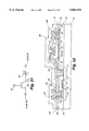
- FIG. 1 A portion of a prior art integrated circuit ferroelectric memory cell 10 including a transistor and a ferroelectric capacitor is shown in FIG. 1.
- a silicon or other substrate 12 includes a diffused region 14, which forms part of a transistor used in the memory cell.
- a thick oxide layer 16 forms the substrate for the ferroelectric capacitor.
- the thick oxide layer 16 is patterned and etched to allow access to diffused region 14.
- the ferroelectric capacitor includes a platinum bottom electrode 18, a ferroelectric layer 20, typically PZT (lead zirconate titanate), and a platinum top electrode 22.
- a subsequent oxide layer 24 is deposited, which is patterned and etched, to provide access to diffused region 14, bottom electrode 18, and to top electrode 22.
- a local interconnect layer 26 is deposited, patterned and etched, to provide a local interconnect 26A between top electrode 22 and diffused region 14, as well as metalization 26B for bottom electrode 18.
- ferroelectric materials particularly PZT
- PZT PZT
- One source of hydrogen can be found in the plastic packaging materials often used with integrated circuits.
- Another source of hydrogen can be found in the various oxide layers used in fabricating the ferroelectric capacitor or memory cell.
- a section 28 of memory cell 10 is shown in greater magnification in FIG. 2 to illustrate the problem of hydrogen sensitivity that exists within the prior art memory cell.
- Section 28 shows oxide layer 16, bottom electrode 18, ferroelectric layer 20, top electrode 22, oxide layer 24, and local interconnect 26A. Note particularly in FIG. 2 that there is an interface between oxide layer 24 and ferroelectric layer 20. The interface extends along the top surface and sides of ferroelectric layer 20.
- hydrogen is generated within oxide layer 24, which in turn is gradually absorbed by ferroelectric layer 20.
- the arrows shown in FIG. 2 show generally the probable path of hydrogen diffusion into the ferroelectric layer 20. Studies have shown that exposure to hydrogen gradually degrades the amount of switching charge produced by the ferroelectric capacitor. Over time, the exposure to hydrogen may destroy electrical switching performance altogether.
- capacitor fabricated as set forth herein can be used in a wide array of electronic products such as integrated circuit memories and other integrated circuits, RF/ID integrated circuits and cards, discrete devices, or any application in which improved electrical switching performance and resistance to hydrogen diffusion is desired.
- a ferroelectric capacitor includes a bottom electrode, a top electrode, and a ferroelectric layer located between the top and bottom electrodes that extends to completely encapsulate the top electrode, except for a contact hole to allow metalization of the top electrode.
- the total encapsulation of the top electrode reduces the sensitivity of the ferroelectric capacitor to hydrogen and thus improves electrical switching performance.
- a ferroelectric capacitor includes a bottom electrode and a ferroelectric layer formed on the bottom electrode.
- the ferroelectric layer is partially etched to form an indentation to receive a top electrode.
- a dielectric layer is formed over the ferroelectric layer, and includes a contact hole to allow metalization of the top electrode. The partial encapsulation of the top electrode also reduces the sensitivity of the ferroelectric capacitor to hydrogen.
- the ferroelectric layer in the capacitor can be fabricated using PZT, SBT, or other known ferroelectric materials.
- the ferroelectric capacitor can then be used in conjunction with a transistor to form a memory cell in an array of such cells.
- a first method of fabricating a ferroelectric capacitor according to the present invention includes the steps of: forming in sequence a bottom electrode layer, a first ferroelectric layer, and a top electrode layer; etching the top electrode layer to form a top electrode; forming a second ferroelectric layer over the first ferroelectric layer, thereby completely encapsulating the top electrode; etching the second ferroelectric layer; etching the first ferroelectric layer and the bottom electrode layer to form a bottom electrode; forming a dielectric layer over the etched first ferroelectric and second ferroelectric layers; etching a contact hole through the dielectric layer and the second ferroelectric layer to allow metalization of the top electrode; and etching a contact hole through the dielectric layer and the first ferroelectric layer to allow metalization of the bottom electrode.
- a second method of fabricating a ferroelectric capacitor according to the present invention includes the steps of: forming in sequence a bottom electrode layer, a first ferroelectric layer, and a top electrode layer; etching the top electrode layer to form a top electrode; etching the first ferroelectric layer; etching the bottom electrode layer to form a bottom electrode; forming a second ferroelectric layer over the first ferroelectric layer, thereby completely encapsulating the top electrode; etching the second ferroelectric layer so that the second ferroelectric layer overlaps the bottom electrode; forming a dielectric layer over the etched second ferroelectric layer; and etching contact holes through the dielectric layer and the second ferroelectric layer to allow metalization of the top and bottom electrodes.
- a third method of fabricating a ferroelectric capacitor according to the present invention includes the steps of: forming in sequence a bottom electrode layer, a first ferroelectric layer, and a top electrode layer; etching the top electrode layer to form a top electrode; etching the first ferroelectric layer; etching the bottom electrode layer to form a bottom electrode; forming a second ferroelectric layer over the first ferroelectric layer, thereby completely encapsulating the top electrode; forming a dielectric layer over the second ferroelectric layer; and etching contact holes through the dielectric layer and the second ferroelectric layer to allow metalization of the top and bottom electrodes.
- a fourth method of fabricating a ferroelectric capacitor according to the present invention includes the steps of: forming in sequence a bottom electrode layer, a first ferroelectric layer of a first thickness, and a top electrode layer; etching the top electrode layer to form a top electrode; etching the first ferroelectric layer; forming a second ferroelectric layer of a second thickness over the first ferroelectric layer, thereby completely encapsulating the top electrode; etching the second ferroelectric layer and the bottom electrode layer to form a bottom electrode; forming a dielectric layer over the etched second ferroelectric layer; and etching contact holes through the dielectric layer and the second ferroelectric layer to allow metalization of the top and bottom electrodes.
- a fifth method of fabricating a ferroelectric capacitor according to the present invention includes the steps of: forming in sequence a bottom electrode layer and a ferroelectric layer; partially etching the ferroelectric layer to form an indentation; forming a conformal top electrode layer over the ferroelectric layer; etching away the top electrode layer to form a top electrode in the indentation; etching the ferroelectric layer; etching the bottom electrode layer to form a bottom electrode; forming a dielectric layer over the etched ferroelectric layer; and etching contact holes through the dielectric layer to allow metalization of the top and bottom electrodes.
- a sixth method of fabricating a ferroelectric capacitor according to the present invention includes the steps of: forming a bottom electrode layer; etching the bottom electrode layer to form a bottom electrode; forming a ferroelectric layer over the bottom electrode; partially etching the ferroelectric layer to form an indentation; forming a conformal top electrode layer over the ferroelectric layer; etching away the top electrode layer to form a top electrode in the indentation; forming a dielectric layer over the ferroelectric layer; etching a contact hole through the dielectric layer to allow metalization of the top electrodes; and etching a contact hole through the dielectric layer and the ferroelectric layer to allow metalization of the bottom electrode.
- An integrated circuit ferroelectric memory cell having a bit line, a word line, and a plate line, fabricated according to the present invention includes: a silicon substrate or epitaxial region; a transistor formed in the substrate including first and second diffused regions, a thin gate oxide, and a gate forming the word line; a thick oxide layer formed on the substrate including contact holes to allow metalization of the first and second diffused regions; a ferroelectric capacitor formed on the thick oxide layer, the ferroelectric capacitor including a bottom electrode, a ferroelectric layer, and a top electrode, wherein the ferroelectric layer either partially or completely encapsulates the top electrode and includes a contact hole to allow metalization of the top electrode; a first dielectric layer formed over the thick oxide layer and the ferroelectric capacitor including contact holes to allow metalization of the first and second diffused regions, and the top and bottom electrodes of the ferroelectric capacitor; a first patterned metalization layer for contacting the first diffused region, for forming a local interconnect between the top electrode and the second diffused region,
- FIG. 1 is a sectional view of a portion of a prior art integrated circuit ferroelectric memory including a ferroelectric capacitor and a transistor;
- FIG. 2 is a magnified view of a prior art ferroelectric capacitor illustrating particularly the problem of hydrogen diffusion into the ferroelectric dielectric layer resulting in degradation of electrical switching performance;
- FIGS. 3-9 are sequential sectional views of a ferroelectric capacitor process suitable for use in a ferroelectric memory having decreased hydrogen sensitivity according to a first embodiment of the invention
- FIG. 10 is a plan view of a set of ferroelectric capacitors fabricated according to the process shown in FIGS. 3-9;
- FIGS. 11-17 are sequential sectional views of a ferroelectric capacitor process suitable for use in a ferroelectric memory having decreased hydrogen sensitivity according to a second embodiment of the invention.
- FIG. 18 is a plan view of a set of ferroelectric capacitor fabricated according to the process shown in FIGS. 11-17;
- FIGS. 19-24 are sequential sectional views of a ferroelectric capacitor process suitable for use in a ferroelectric memory having decreased hydrogen sensitivity according to a third embodiment of the invention.
- FIG. 25 is a plan view of a set of ferroelectric capacitor fabricated according to the process shown in FIGS. 19-24;
- FIGS. 26-32 are sequential sectional views of a ferroelectric capacitor process suitable for use in a ferroelectric memory having decreased hydrogen sensitivity according to a fourth embodiment of the invention.
- FIGS. 33-41 are sequential sectional views of a ferroelectric capacitor process suitable for use in a ferroelectric memory having decreased hydrogen sensitivity according to a fifth embodiment of the invention.
- FIGS. 42-50 are sequential sectional views of a ferroelectric capacitor process suitable for use in a ferroelectric memory having decreased hydrogen sensitivity according to a sixth embodiment of the invention.
- FIG. 51 is a schematic diagram of a ferroelectric memory cell having a transistor and a ferroelectric capacitor
- FIG. 52 is a sectional view of a completely metalized integrated circuit ferroelectric memory, in which the top electrode of the ferroelectric capacitor is completely encapsulated according to the present invention
- FIG. 53 is a cross sectional view of a discrete ferroelectric capacitor having a large top electrode used for testing purposes, but having a top electrode opening about the same area as that used for ferroelectric memory array capacitors;
- FIG. 54 is a hysteresis loop that illustrates the charge versus applied voltage switching behavior of a ferroelectric capacitor, particularly illustrating switched charge (QSW).
- FIG. 55 is a graph of applied switching voltage level versus switched charge for a ferroelectric capacitor, particularly illustrating V(90%), or the voltage level at which switched charge attains about 90% of its final value.
- FIGS. 3-9 sequential sectional views of a first ferroelectric capacitor process suitable for use in a ferroelectric memory having decreased hydrogen sensitivity are shown.
- a layer 16 of BPSG glass about 7000 Angstroms thick is deposited onto a silicon or other substrate (not shown). Any oxide, nitride, or other appropriate dielectric layer can be substituted for BPSG layer 16.
- a platinum bottom electrode layer 18 is subsequently deposited over BPSG glass layer 16 to a thickness of about 1750 Angstroms. While platinum is used for electrode layer 16, other known materials compatible with ferroelectric films can be used including iridium, iridium oxide, and the like.
- the bottom electrode layer 18 also includes a titanium adhesion layer about 200 Angstroms thick to facilitate the adhesion of the platinum bottom electrode layer 18 to BPSG glass layer 16.
- a first ferroelectric layer 20 is subsequently deposited over the bottom electrode layer 18 to a thickness of about 3000 Angstroms.
- the material used in ferroelectric layer 20 is ideally doped or undoped PZT (lead zirconate titanate), SBT (strontium bismuth tantalate), or any other known ferroelectric material suitable for use in thin film form.
- a first anneal is performed. The first anneal includes a 650° C. heat treatment for about five seconds, followed by an 850° C. heat treatment for about five seconds.
- a platinum top electrode layer 22 is subsequently deposited over the first ferroelectric layer 20 to a thickness of about 1750 Angstroms.
- the material used in top electrode layer 22 can be other than platinum as described above.
- Top electrode layer 22 is etched to form one or more top electrodes. Platinum is typically etched using a reactive-ion etch in an argon and chlorine atmosphere, although other gases can be used. Ion milling can be used as well as an alternative etching technique.
- the dimensions of the individual top electrodes can modified as desired from nominal dimensions of 1.5 ⁇ 1.5 microns, with a spacing of about three microns between top electrodes.
- a second anneal is performed. The second anneal includes a 650° C. heat treatment for about sixty minutes in an oxygen atmosphere.
- a second "cap" ferroelectric layer 30 about the same thickness (3000 Angstroms) as the first ferroelectric layer 20 is deposited over the first ferroelectric layer 20, thereby completely encapsulating the top electrodes 22.
- the material used in the second ferroelectric layer 30 is also ideally doped or undoped PZT (lead zirconate titanate), SBT (strontium bismuth tantalate), or any other known ferroelectric material suitable for use in thin film form.
- the first and second ferroelectric layers need not be the same ferroelectric material, since the second layer is used for its resistance to hydrogen diffusion or hydrogen "gettering" properties and not specifically for its ferroelectric properties.
- an optional third anneal can be performed.
- the optional third anneal includes a 650° C. heat treatment for about sixty minutes in an oxygen atmosphere.
- the second ferroelectric layer 30 is etched according to the same etching method as set forth for the first ferroelectric layer 20.
- the second ferroelectric layer 30 is etched to leave a reasonable overlap of the top electrodes 22, about 1.5 to 2.0 microns.
- the first ferroelectric layer 20 and the bottom electrode layer 18 are simultaneously etched to define the dimensions of a bottom electrode. As can be seen in FIG. 6, one end of the bottom electrode 18 is etched to allow sufficient room for an eventual bottom electrode contact. The other end of bottom electrode 18 is etched to the same dimensions as the second ferroelectric layer 30.
- the first ferroelectric layer 20 and the bottom electrode layer 18 are simultaneously etched using a reactive-ion etch in an argon and carbon tetrafluoride atmosphere, although other gases can be used. Ion milling can also be used as an alternative etching technique.
- an optional first recovery anneal can be performed.
- the optional first recovery anneal includes a 550° C. heat treatment for about sixty minutes in an oxygen atmosphere.
- a PTEOS glass dielectric layer 24 is deposited over the etched first ferroelectric and second ferroelectric layers 20 and 30 to a thickness of about 5000 Angstroms. Other dielectric layers can be used for dielectric layer 24.
- contact holes are etched to provide access of the top and bottom electrodes 22 and 18.
- Contact hole 32 provides access to bottom electrode 18, and contact holes 34 provide access to top electrodes 22.
- Contact holes 34 are etched through the dielectric layer 24 and the second ferroelectric layer 30 to allow metalization of the top electrodes.
- Contact hole 32 is etched through the dielectric layer 24 and the first ferroelectric layer 20 to allow metalization of bottom electrode 18. Note that the contact holes 32 and 34 are ideally etched in two steps. The first etching step removes the dielectric layer 24 in the contact holes.
- the dielectric oxide material can be etched away using a fluorine-based wet or dry etch. It is desirable that a sloped profile is etched into the contact holes.
- the remaining ferroelectric material in the contact hole is etched away according to the ferroelectric etch described above. Note in FIG. 8 that contact holes 32 and 34 are etched through about the same thickness of material, i.e. 5000 Angstroms of glass plus 3000 Angstroms of ferroelectric material. Therefore, the etching of contact holes 32 and 34 can be performed simultaneously.
- an optional second recovery anneal can be performed. The optional second recovery anneal includes a 550° C. heat treatment for about sixty minutes in an oxygen atmosphere.
- contact holes 32 and 34 are metalized to provide electrical access to bottom electrode 18 and top electrodes 22.
- a titanium nitride local interconnect metalization layer is deposited to a thickness of about 800 Angstroms and etched to form a metal contact 36 for bottom electrode 18 and a metal contact 38 for each of the top electrodes 22.
- the full metalization scheme showing subsequent oxide and metalization layers for a ferroelectric memory cell is shown in FIG. 52, although other metalization schemes can be used.
- a titanium layer about 1500 Angstroms thick followed by an aluminum layer of about 8000 Angstroms thick can be used to form metal contacts 36 and 38.
- Other metalization techniques can be used as well after the titanium nitride layer has been deposited.
- FIG. 10 A plan view of the capacitor structure described above with respect to FIGS. 3-9 is shown in FIG. 10.
- the bottom electrode 18 and first ferroelectric layer 20 are shown as coincident layers forming a first rectangle.
- a second, smaller rectangle is formed of the bottom electrode 18, the first ferroelectric layer 20, and the second ferroelectric layer 30.
- the contact holes to the bottom and top electrodes 32 and 34 are shown as circular features.
- the local interconnect metal contact straps 38 that contact the top electrodes 22 are shown as individual rectangles overlapping contact holes 34 and 40.
- Contact holes 40 are not shown in FIGS. 3-9 but represent a contact to another structure such as the diffused region of a transistor as is shown in FIG. 52.
- FIGS. 11-17 sequential sectional views of a second ferroelectric capacitor process suitable for use in a ferroelectric memory having decreased hydrogen sensitivity are shown.
- FIG. 11 is the same sectional view as FIG. 3, showing the sequential deposition of a thick glass layer 16, a bottom electrode layer 18, a first ferroelectric layer 20, and a top electrode layer 22. All of the thicknesses and materials described above are the same in FIG. 11.
- a first anneal can be performed after the first ferroelectric layer 18 is deposited.
- the platinum top electrode layer 22 is etched to form individual top electrodes 22.
- a second anneal can be performed after the top electrodes 22 are etched.
- the first ferroelectric layer 20 is etched with some lateral overlap of the etched top electrodes 20.
- the bottom electrode layer 18 is etched to define the dimensions of a bottom electrode. As can be seen in FIG. 12, one end of the bottom electrode 18 is etched to allow sufficient room for the eventual bottom electrode contact. The other end of bottom electrode 18 is etched to the same dimensions as the first ferroelectric layer 20.
- the etching techniques for bottom electrode 18 and first ferroelectric layer 20 are as described above with reference to FIGS. 3-11.
- an optional first recovery anneal can be performed.
- the optional first recovery anneal includes a 550° C. heat treatment for about sixty minutes in an oxygen atmosphere.
- a second "cap" ferroelectric layer 30 about the same thickness (3000 Angstroms) as the first ferroelectric layer 20 is deposited over the first ferroelectric layer 20, thereby completely encapsulating the top electrodes 22.
- an optional third anneal can be performed.
- the optional third anneal includes a 650° C. heat treatment for about sixty minutes in an oxygen atmosphere.
- the second ferroelectric layer 30 is etched according to the same etching method as set forth for the first ferroelectric layer 20.
- the second ferroelectric layer 30 is etched to leave a reasonable overlap of the bottom electrode 18, about 1.5 to 2.0 microns.
- an optional second recovery anneal can be performed.
- a PTEOS glass dielectric layer 24 is deposited over the etched second ferroelectric layers 30 to a thickness of about 5000 Angstroms.
- contact holes are etched to provide access of the top and bottom electrodes 22 and 18.
- Contact hole 32 provides access to bottom electrode 18, and contact holes 34 provide access to top electrodes 22.
- both contact holes 34 and 36 are etched through the dielectric layer 24 and the second ferroelectric layer 30 to allow metalization of the top and bottom electrodes.
- the thickness of contact holes 34 and 36 is the same since they are etched through the same thickness of material.
- Contact holes 32 and 34 are ideally simultaneously etched in two steps to remove the dielectric oxide material and then the remaining ferroelectric material. The type of etch used in the same as described with reference to FIG. 8. After contact holes 32 and 34 are etched, an optional second recovery anneal can be performed.
- contact holes 32 and 34 are metalized to provide electrical access to bottom electrode 18 and top electrodes 22.
- a titanium nitride local interconnect metalization layer is deposited to a thickness of about 800 Angstroms and etched to form a metal contact 36 for bottom electrode 18 and a metal contact 38 for each of the top electrodes 22.
- the full metalization scheme showing subsequent oxide and metalization layers for a ferroelectric memory cell is shown in FIG. 52, although other metalization schemes can be used.
- FIG. 18 A plan view of the capacitor structure described above with respect to FIGS. 11-17 is shown in FIG. 18.
- the bottom electrode 18 is shown as forming a first rectangle.
- a second, smaller rectangle is formed of the bottom electrode 18 and the first ferroelectric layer 20.
- the second ferroelectric layer 30 is shown as a dashed rectangle overlapping the bottom electrode 18.
- the contact holes to the bottom and top electrodes 32 and 34 are shown as circular features.
- the local interconnect metal contact straps 38 that contact the top electrodes 22 are shown as individual rectangles overlapping contact holes 34 and 40.
- Contact holes 40 are not shown in FIGS. 11-17 but represent a contact to another structure such as the diffused region of a transistor as is shown in FIG. 52.
- FIGS. 19-24 sequential sectional views of a third ferroelectric capacitor process suitable for use in a ferroelectric memory having decreased hydrogen sensitivity are shown.
- FIGS. 19-21 are identical to previously described FIGS. 11-13 both in sectional views, material, etching, and annealing steps.
- FIG. 19 shows a thick glass layer 16, a bottom electrode layer 18, a first ferroelectric layer 20, and a top electrode layer 22 formed in sequence, wherein the top electrode layer 22 is etched to form individual top electrodes 22.
- FIG. 20 shows the etching of the first ferroelectric layer 20 and the etching of the bottom electrode layer 18 to form a bottom electrode.
- a second "cap" ferroelectric layer 30 about the same thickness (3000 Angstroms) as the first ferroelectric layer 20 is deposited over the first ferroelectric layer 20, thereby completely encapsulating the top electrodes 22.
- a first anneal is performed after the ferroelectric layer 20 is deposited, a second anneal is performed after the top electrode layer 22 is etched, and an optional third anneal is performed after the second ferroelectric layer 30 is deposited.
- a optional first recovery anneal is performed after the first ferroelectric layer 20 and bottom electrode layer 18 have been etched.
- a PTEOS glass dielectric layer 24 is deposited over the unetched second ferroelectric layer 30 to a thickness of about 5000 Angstroms.
- contact holes are etched to provide access of the top and bottom electrodes 22 and 18.
- Contact hole 32 provides access to bottom electrode 18, and contact holes 34 provide access to top electrodes 22.
- both contact holes 34 and 36 are etched through the dielectric layer 24 and the second ferroelectric layer 30 to allow metalization of the top and bottom electrodes.
- the thickness of contact holes 34 and 36 is the same since they are etched through the same thickness of material.
- Contact holes 32 and 34 are ideally simultaneously etched in two steps to remove the dielectric oxide material and then the remaining ferroelectric material. The type of etch used in the same as described with reference to FIG. 8.
- a second optional recovery anneal can be performed after contact holes 32 and 34 have been opened.
- contact holes 32 and 34 are metalized to provide electrical access to bottom electrode 18 and top electrodes 22.
- a titanium nitride local interconnect metalization layer is deposited to a thickness of about 800 Angstroms and etched to form a metal contact 36 for bottom electrode 18 and a metal contact 38 for each of the top electrodes 22.
- the full metalization scheme showing subsequent oxide and metalization layers for a ferroelectric memory cell is shown in FIG. 52, although other metalization schemes can be used.
- FIG. 25 A plan view of the capacitor structure described above with respect to FIGS. 19-24 is shown in FIG. 25.
- the bottom electrode 18 is shown as forming a first rectangle.
- a second, smaller rectangle is formed of the bottom electrode 18 and the first ferroelectric layer 20.
- the second ferroelectric layer 30 is shown as a dashed rectangle overlapping the bottom electrode 18 by a wide margin. The wide margin shown is meant to convey the unetched, continuous extent of the second ferroelectric layer 30.
- the contact holes to the bottom and top electrodes 32 and 34 are shown as circular features.
- the local interconnect metal contact straps 38 that contact the top electrodes 22 are shown as individual rectangles overlapping contact holes 34 and 40. Contact holes 40 are not shown in FIGS. 19-24 but represent a contact to another structure such as the diffused region of a transistor as is shown in FIG. 52.
- FIGS. 26-32 sequential sectional views of a fourth ferroelectric capacitor process suitable for use in a ferroelectric memory having decreased hydrogen sensitivity are shown.
- the fourth ferroelectric capacitor process described below allows the thickness of the second ferroelectric layer 30 to be different from the first ferroelectric layer 20, if desired.
- FIG. 26 is the same as previously described FIGS. 3, 11, and 19.
- a first anneal is performed after the first ferroelectric layer 20 is deposited, and a second anneal is performed after the top electrode layer 22 is etched.
- FIG. 27 only the first ferroelectric layer 20 is etched to a reasonable overlap of the etched top electrodes 22.
- the bottom electrode layer 18 remains unetched in FIG. 27.
- An optional first recovery anneal is performed after the first ferroelectric layer 20 is etched.
- a second "cap" ferroelectric layer 30' of a different thickness (less than or greater than 3000 Angstroms) from the first ferroelectric layer 20 is deposited over the first ferroelectric layer 20, thereby completely encapsulating the top electrodes 22.
- a less thick second ferroelectric layer 30' is desirable since less material is used, it is easier to etch, more planar, and for other processing reasons. However, if desired, the same or a thicker ferroelectric layer 30' can be used.
- the material used for the second ferroelectric layer 30' is the same as described above, and can be different than the material used in the first ferroelectric layer 20.
- An optional third anneal can be performed after the second ferroelectric layer 30' is deposited.
- the second ferroelectric layer 30' and the bottom electrode layer 18 are simultaneously etched to form a bottom electrode.
- an optional second recovery anneal can be performed.
- a PTEOS glass dielectric layer 24 is deposited over the etched second ferroelectric layer 30' to a thickness of about 5000 Angstroms.
- contact holes are etched to provide access of the top and bottom electrodes 22 and 18.
- Contact hole 32 provides access to bottom electrode 18, and contact holes 34 provide access to top electrodes 22.
- both contact holes 34 and 36 are etched through the dielectric layer 24 and the second ferroelectric layer 30' to allow metalization of the top and bottom electrodes.
- the thickness of contact holes 34 and 36 is the same since they are etched through the same thickness of material.
- Contact holes 32 and 34 are ideally simultaneously etched in two steps to remove the dielectric oxide material and then the remaining ferroelectric material. The type of etch used in the same as described with reference to FIG. 8. After contact holes 32 and 34 have been etched, an optional third recovery anneal can be performed.
- contact holes 32 and 34 are metalized to provide electrical access to bottom electrode 18 and top electrodes 22.
- the full metalization scheme showing subsequent oxide and metalization layers for a ferroelectric memory cell is shown in FIG. 52, although other metalization schemes can be used.
- a plan view of the capacitor structure described above with respect to FIGS. 26-32 is not shown, but is similar to the plan view shown in FIG. 18. The one difference is that the second ferroelectric layer 30' does not overlap the bottom electrode 18, but is coincident thereto.
- FIGS. 33-41 sequential sectional views of a fifth ferroelectric capacitor process suitable for use in a ferroelectric memory having decreased hydrogen sensitivity are shown.
- a layer 16 of BPSG glass about 7000 Angstroms thick is deposited onto a silicon or other substrate (not shown).
- a platinum bottom electrode layer 18 is subsequently deposited over BPSG glass layer 16 to a thickness of about 1750 Angstroms.
- the bottom electrode layer 18 also includes a titanium adhesion layer about 200 Angstroms thick to facilitate the adhesion of the platinum bottom electrode layer 18 to BPSG glass layer 16.
- a ferroelectric layer 20 is subsequently deposited over the bottom electrode layer 18 to a thickness of about 3000 Angstroms.
- the material used in ferroelectric layer 20 is ideally doped or undoped PZT (lead zirconate titanate), SBT (strontium bismuth tantalate), or any other known ferroelectric material suitable for use in thin film form.
- the ferroelectric layer 20 is partially etched to form one or more indentations 42.
- Indentations 42 should be etched to a sufficient depth to completely receive the top electrodes as is explained in further detail below.
- the etching technique used is the same reactive-ion etch used in etching the ferroelectric layers.
- a first anneal is performed. The first anneal includes a 650° C. heat treatment for about five seconds, followed by an 850° C. heat treatment for about five seconds.
- a platinum top electrode layer 22 is subsequently deposited over the ferroelectric layer 20 to a thickness of about 1750 Angstroms.
- the top electrode layer 22 is conformal and thus fills in each of the indentations 42.
- the top electrode layer 22 is etched away to form one or more top electrodes in indentations 42.
- Platinum is typically etched using a reactive-ion etch in an argon and chlorine atmosphere.
- Alternative etching techniques include ion milling or chemical mechanical polishing (CMP).
- CMP chemical mechanical polishing
- the dimensions of the individual top electrodes can modified as desired from nominal dimensions of 1.5 ⁇ 1.5 microns, with a spacing of about three microns between top electrodes.
- a second anneal is performed.
- the second anneal includes a 650° C. heat treatment for about sixty minutes in an oxygen atmosphere.
- the ferroelectric layer 20 is etched to leave a reasonable lateral overlap of the top electrodes 22.
- the bottom electrode layer 18 is etched to define the dimensions of a bottom electrode. As can be seen in FIG. 38, one end of the bottom electrode 18 is etched to allow room for an eventual bottom electrode contact. The other end of bottom electrode 18 is etched to the same dimensions as the second ferroelectric layer 30.
- the bottom electrode layer 18 is etched using a reactive-ion etch in an argon and chlorine atmosphere. After the bottom electrode layer 18 is etched, an optional first recovery anneal can be performed.
- the optional first recovery anneal includes a 550° C. heat treatment for about sixty minutes in an oxygen atmosphere.
- a PTEOS glass dielectric layer 24 is deposited over the etched ferroelectric layer 20 to a thickness of about 5000 Angstroms.
- contact holes are etched to provide access of the top and bottom electrodes 22 and 18.
- Contact hole 32 provides access to bottom electrode 18, and contact holes 34 provide access to top electrodes 22.
- Contact holes 34 and 32 are etched through the dielectric layer 24 to allow metalization of the top electrodes and bottom electrodes 22 and 18. Note that the contact holes 32 and 34 are etched in a single etching step.
- the dielectric oxide material can be etched away using a fluorine-based wet or dry etch. It is desirable that a sloped profile is etched into the contact holes. Note in FIG. 40 that contact holes 32 and 34 are etched through about the same thickness of material, i.e. 5000 Angstroms of glass dielectric layer 24.
- a second optional recovery anneal can be performed after contact holes 32 and 34 are opened as previously described.
- contact holes 32 and 34 are metalized to provide electrical access to bottom electrode 18 and top electrodes 22 as previously described above.
- a plan view of the capacitor structure described above with respect to FIGS. 33-41 is similar to that shown in FIG. 10. The only difference is that there is no second level of ferroelectric material 30. The contours of the plan view, however, are the same.
- FIGS. 42-50 sequential sectional views of a sixth ferroelectric capacitor process suitable for use in a ferroelectric memory having decreased hydrogen sensitivity are shown.
- a layer 16 of BPSG glass about 7000 Angstroms thick is deposited onto a silicon or other substrate (not shown).
- a platinum bottom electrode layer 18 is subsequently deposited over BPSG glass layer 16 to a thickness of about 1750 Angstroms.
- the bottom electrode layer 18 also includes a titanium adhesion layer about 200 Angstroms thick to facilitate the adhesion of the platinum bottom electrode layer 18 to BPSG glass layer 16.
- bottom electrode layer 18 is etched to form a bottom electrode.
- a ferroelectric layer 20 is subsequently deposited over the bottom electrode 18 to a thickness of about 3000 Angstroms.
- the material used in ferroelectric layer 20 is ideally doped or undoped PZT (lead zirconate titanate), SBT (strontium bismuth tantalate), or any other known ferroelectric material suitable for use in thin film form.
- the ferroelectric layer 20 is partially etched to form one or more indentations 42.
- Indentations 42 should be etched to a sufficient depth to completely receive the top electrodes as is explained in further detail below.
- the etching technique used is the same reactive-ion etch used in etching the ferroelectric layers.
- a first anneal is performed. The first anneal includes a 650° C. heat treatment for about five seconds, followed by an 850° C. heat treatment for about five seconds.
- a platinum top electrode layer 22 is subsequently deposited over the ferroelectric layer 20 to a thickness of about 1750 Angstroms.
- the top electrode layer 22 is conformal and thus fills in each of the indentations 42.
- the top electrode layer 22 is etched away to form one or more top electrodes in indentations 42. Platinum is typically etched using a reactive-ion etch in an argon and chlorine atmosphere. The dimensions of the individual top electrodes can modified as desired from nominal dimensions of 1.5 ⁇ 1.5 microns, with a spacing of about three microns between top electrodes.
- a second anneal is performed. The second anneal includes a 650° C. heat treatment for about sixty minutes in an oxygen atmosphere.
- a PTEOS glass dielectric layer 24 is deposited over the etched ferroelectric layer 20 to a thickness of about 5000 Angstroms.
- contact holes are etched to provide access of the top and bottom electrodes 22 and 18.
- Contact hole 32 provides access to bottom electrode 18, and contact holes 34 provide access to top electrodes 22.
- Contact holes 34 are etched through the dielectric layer 24 to allow metalization of the top electrodes 22.
- Contact hole 32 is etched through dielectric layer 24 as well as ferroelectric layer 20. Note, therefore, that contact holes 32 and 34 are etched in two separate etching steps.
- the dielectric oxide material can be etched away using a fluorine-based wet or dry etch.
- the ferroelectric material is etched used a reactive-ion etch. It is desirable that a sloped profile is etched into the contact holes. An optional recovery anneal can be performed at this point in the process.
- contact holes 32 and 34 are metalized to provide electrical access to bottom electrode 18 and top electrodes 22 as previously described above.
- a plan view of the capacitor structure described above with respect to FIGS. 42-50 is similar to that shown in FIG. 25. The differences are that there is no second level of ferroelectric material 30, and the contour for ferroelectric material 20 should be removed.
- FIG. 51 a schematic diagram for a typical non-volatile ferroelectric memory is shown having a transistor 52 coupled to a ferroelectric capacitor 54.
- the configuration in FIG. 51 is known as a one-transistor, one-capacitor ferroelectric memory cell or "1T/1C" cell.
- One current node of the transistor 52 forms the bit line of the cell, and is designated 14, 46, 48 to correspond to regions in the integrated cell shown below in FIG. 52.
- the other current node of transistor 52 is coupled to ferroelectric capacitor 54 at node 56.
- the gate 15 of transistor 52 forms the word line of the memory cell.
- One end of capacitor 54 is coupled to transistor 52 at node 56, and the other end of capacitor 54 forms the plate line of the memory cell.
- the plate line node is designated 18, 36, 48 to correspond to regions in the integrated cell shown below in FIG. 52.
- FIG. 52 a sectional view of a completely metalized integrated circuit ferroelectric memory cell having a bit line, a word line, and a plate line is shown.
- the memory cell includes a silicon substrate or epitaxial region 12, and a transistor formed in the substrate 12 including first and second diffused regions 14, a thin gate oxide 13, and a gate 15 forming the word line.
- a thick oxide layer 16 is formed on the substrate 12 including contact holes to allow metalization of the first and second diffused regions 14. Note that in FIG. 52, the exact sequence for forming each of the various layers and contact holes within each layer is not fully described; the contact holes may actually be formed at a subsequent processing step.
- a ferroelectric capacitor is subsequently formed on the thick oxide layer 16, including a bottom electrode 18, a ferroelectric layer 20+30, and a top electrode 22, wherein the ferroelectric layer 20+30 either partially or completely encapsulates the top electrode 22.
- the ferroelectric layer 20+30 includes a contact hole to allow metalization of the top electrode 22.
- a first dielectric layer 24 is formed over the thick oxide layer 16 and the ferroelectric capacitor, including contact holes to allow metalization of the first and second diffused regions 14, and the top and bottom electrodes 22 and 18 of the ferroelectric capacitor.
- a first patterned metalization layer 36, 38, 46 is deposited for contacting the first diffused region 14 with metal contact 46, for forming a local interconnect 38 between the top electrode 22 and the second diffused region 14, and for metalizing the bottom electrode 36 with metal contact 36.
- a second dielectric layer 44 is formed over the first metalization layer 36, 38, 46 including contact holes to allow metalization of the first diffused region 14 and the bottom electrode 36.
- a second patterned metalization layer 48 contacts the first diffused region 14 and forms the bit line of the memory cell, and contacts the bottom electrode 18 to form the plate line of the memory cell.
- a passivation layer 50 is formed over the second metalization layer 48.
- first and second dielectric layers 24 and 44 are typically thin doped or undoped oxide layers, if greater resistance to hydrogen diffusion is required these layers can also be made of ferroelectric materials such as PZT or SBT. Still further, the passivation layer 50, while typically formed of silicon nitride or the like, can also be made from ferroelectric materials such as PZT or SBT. All three layers mentioned above can be fabricated of the same or different ferroelectric materials as desired, and not necessarily the same material as used in the ferroelectric layer of the ferroelectric capacitor. Further teachings regarding ferroelectric material passivation can be found in U.S. Pat. No.
- the device structures according to the present invention provide a measure of immunity to line degradation associated with exposure to hydrogen during various processing steps. Additionally, it has been discovered that the method and structures of the present invention provide a significant improvement in several key ferroelectric performance parameters, as is explained in further detail below. Data supporting these discoveries is also provided below.
- the key ferroelectric performance parameters listed below are: opposite state charge; opposite state charge aging rate; V(90%), which is the voltage level at which the switched charge reaches about 90% of its final value; switched charge; and fatigued switched charge measured at some known number of switching cycles.
- the improvement in the above-listed performance parameters was measured on a partially formed "unencapsulated" ferroelectric capacitor such as can be seen in FIGS. 1, 2, 3, 11, 12, 19, 20, 26, or 27, relative to the performance parameters measured on a fully formed, totally encapsulated ferroelectric capacitor such as can be seen in FIGS. 24, 32, or 52.
- the improvement must be measured between an unencapsulated reference capacitor (the structure of which can be seen in FIG. 1 or FIG. 2, for example) of similar size to the fully formed, partially encapsulated ferroelectric capacitor. This is because, as can be seen from an inspection of FIGS. 33-41 and FIGS. 42-50, there is no partially formed unencapsulated ferroelectric capacitor whose base line performance can be measured.
- FIG. 53 is a cross sectional diagram of a typical discrete ferroelectric capacitor used for testing purposes in which the area of the top electrode contact opening 34 is small with respect to the area of the large top electrode 22'.
- Memory array capacitors according to the present invention are shown in FIGS. 9, 17, 24, 32, 41, 50, and 52 in which the area of the contact opening 34 is the same as in FIG. 53.
- the area of the top electrode 22 in these figures is much smaller than the top electrode 22' shown in FIG. 53, and the ratio of the area of the contact opening 34 to the area of the top electrode 22 is much greater. Studies and data confirm that the improvement in electrical performance is greater in the discrete ferroelectric capacitor of FIG.
- the top electrode 22' of the discrete capacitor shown in FIG. 53 may be more constrained than the top electrodes 22 in the memory array capacitors.
- Opposite State Charge A crucial property of nonvolatile semiconductor memories, and ferroelectric memories in particular is retention in the absence of power. Retention is the ability to maintain a given data state between the time the data state is written and when it is subsequently read. A certain data state is written into a ferroelectric capacitor, or, in the case of a two-transistor, two-capacitor ("2T-2C") memory cell, a complementary data state. After a specified period of time, and at temperature, if desired, the data state is read to determine whether or not the original data state has been retained in the memory cell.
- 2T-2C two-transistor, two-capacitor
- Opposite State Charge Aging Rate Once the opposite state charge has been measured at various points in time, the rate at which this charge decays over time can also be easily calculated. This "opposite state charge aging rate", which is also known as imprint degradation, is also another important indicia of ferroelectric memory performance. The opposite state charge aging rate is calculated in percent of charge loss per natural decade of time. The calculated quantities have a negative value because opposite state charge decays with time and thus has a negative slope value.
- V(90%) A further indicia of ferroelectric memory performance is termed "V(90%)" or the voltage at which the switched charge (QSW) reaches about 90% of its final value.
- Switched charge is the charge component measured between two charge points Q1 and Q2 on a hysteresis curve associated with a ferroelectric capacitor as is shown in FIG. 54.
- the V(90%) value can readily be ascertained by plotting switched charge versus the applied switching voltage level as is shown in FIG. 55. It is desirable that V(90%) be as low as possible.
- a low V(90%) voltage is correlated to acceptable low voltage memory performance.
- Switched Charge was measured with an applied external five volt switching pulse. Switched charge was measured for two unencapsulated ferroelectric capacitors and compared against the switched charge for the same two capacitors in the completed, encapsulated form with the following results:
- Fatigued Switched Charge which is switched charge after the capacitor under test has been repeatedly switched between two polarization states, was measured with an applied external five volt switching pulse after 10 9 switching cycles. Fatigued switched charge was measured for two unencapsulated ferroelectric capacitors and compared against the fatigued switched charge for the same two capacitors in the completed, encapsulated form with the following results:
- the invention can be modified in arrangement and detail without departing from such principles.
- the following aspects of the semiconductor processes described herein can be changed as required: the types of dielectric materials; the thicknesses of the various layers; the types of ferroelectric materials; the etching processes; the electrode materials; and the anneal temperatures, durations, and numbers.
- the specific application of the ferroelectric capacitor of the present invention is not limited to ferroelectric memory cells, although it is ideally suited to that application. We therefore claim all modifications and variation coming within the spirit and scope of the following claims.
Abstract
Description
______________________________________
         Unencapsulated
                     Encapsulated
______________________________________
Capacitor 1
            9.45 micro-Coulombs
                         26.3 micro-Coulombs
Capacitor 2
           13.24 micro-Coulombs
                         18.7 micro-Coulombs
______________________________________
______________________________________
           Unencapsulated
                    Encapsulated
______________________________________
Capacitor 1  -15.1%/decade
                        -5.3%/decade
Capacitor 2  -6.87%/decade
                        -4.7%/decade
______________________________________
______________________________________
            Unencapsulated
                     Encapsulated
______________________________________
Capacitor 1   4.73 volts 4.15 volts
Capacitor 2   4.61 volts 3.79 volts
______________________________________
______________________________________
         Unencapsulated
                     Encapsulated
______________________________________
Capacitor 1
           36.44 micro-Coulombs
                         42.57 micro-Coulombs
Capacitor 2
           25.77 micro-Coulombs
                         33.79 micro-Coulombs
______________________________________
______________________________________
         Unencapsulated
                     Encapsulated
______________________________________
Capacitor 1
           19.69 micro-Coulombs
                         24.14 micro-Coulombs
Capacitor 2
           13.83 micro-Coulombs
                         27.48 micro-Coulombs
______________________________________
Claims (10)
Priority Applications (5)
| Application Number | Priority Date | Filing Date | Title |
|---|---|---|---|
| US08/728,740 US5864932A (en) | 1996-08-20 | 1996-10-11 | Partially or completely encapsulated top electrode of a ferroelectric capacitor |
| EP97306287A EP0837504A3 (en) | 1996-08-20 | 1997-08-19 | Partially or completely encapsulated ferroelectric device |
| JP22407597A JP4511642B2 (en) | 1996-08-20 | 1997-08-20 | Method for manufacturing ferroelectric capacitor |
| US09/085,280 US6211542B1 (en) | 1996-08-20 | 1998-05-27 | Completely encapsulated top electrode of a ferroelectric capacitor using a lead-enhanced escapsulation layer |
| US09/759,128 US6281023B2 (en) | 1996-08-20 | 2001-01-11 | Completely encapsulated top electrode of a ferroelectric capacitor using a lead-enhanced encapsulation layer |
Applications Claiming Priority (2)
| Application Number | Priority Date | Filing Date | Title |
|---|---|---|---|
| US08/700,076 US5920453A (en) | 1996-08-20 | 1996-08-20 | Completely encapsulated top electrode of a ferroelectric capacitor |
| US08/728,740 US5864932A (en) | 1996-08-20 | 1996-10-11 | Partially or completely encapsulated top electrode of a ferroelectric capacitor |
Related Parent Applications (1)
| Application Number | Title | Priority Date | Filing Date |
|---|---|---|---|
| US08/700,076 Continuation-In-Part US5920453A (en) | 1996-08-20 | 1996-08-20 | Completely encapsulated top electrode of a ferroelectric capacitor |
Related Child Applications (1)
| Application Number | Title | Priority Date | Filing Date |
|---|---|---|---|
| US08/828,157 Continuation-In-Part US6027947A (en) | 1996-08-20 | 1997-03-27 | Partially or completely encapsulated top electrode of a ferroelectric capacitor |
Publications (1)
| Publication Number | Publication Date |
|---|---|
| US5864932A true US5864932A (en) | 1999-02-02 |
Family
ID=46253164
Family Applications (1)
| Application Number | Title | Priority Date | Filing Date |
|---|---|---|---|
| US08/728,740 Expired - Lifetime US5864932A (en) | 1996-08-20 | 1996-10-11 | Partially or completely encapsulated top electrode of a ferroelectric capacitor |
Country Status (1)
| Country | Link |
|---|---|
| US (1) | US5864932A (en) |
Cited By (36)
| Publication number | Priority date | Publication date | Assignee | Title |
|---|---|---|---|---|
| US6174735B1 (en) * | 1998-10-23 | 2001-01-16 | Ramtron International Corporation | Method of manufacturing ferroelectric memory device useful for preventing hydrogen line degradation |
| US6197631B1 (en) * | 1997-10-07 | 2001-03-06 | Sharp Kabushiki Kaisha | Semiconductor storage device with a capacitor using a ferroelectric substance and fabricating method thereof |
| US6242299B1 (en) | 1999-04-01 | 2001-06-05 | Ramtron International Corporation | Barrier layer to protect a ferroelectric capacitor after contact has been made to the capacitor electrode |
| US6410345B1 (en) * | 2001-05-11 | 2002-06-25 | Hynix Semiconductor, Inc. | Method for manufacturing a ferroelectric memory device |
| US6423592B1 (en) | 2001-06-26 | 2002-07-23 | Ramtron International Corporation | PZT layer as a temporary encapsulation and hard mask for a ferroelectric capacitor |
| US20020149439A1 (en) * | 2001-04-11 | 2002-10-17 | Toncich Stanley S. | Tunable isolator |
| US20030001151A1 (en) * | 2001-06-29 | 2003-01-02 | Intel Corporation | Discrete polymer memory array and method of making same |
| US20030001176A1 (en) * | 2001-06-29 | 2003-01-02 | Intel Corporation | Low-voltage and interface damage-free polymer memory device |
| US6597028B2 (en) | 2000-06-26 | 2003-07-22 | Ramtron International Corporation | Capacitively coupled ferroelectric random access memory cell and a method for manufacturing the same |
| US20050007291A1 (en) * | 2002-02-12 | 2005-01-13 | Jorge Fabrega-Sanchez | System and method for impedance matching an antenna to sub-bands in a communication band |
| US20050057322A1 (en) * | 2001-04-11 | 2005-03-17 | Toncich Stanley S. | Apparatus and method for combining electrical signals |
| US20050057414A1 (en) * | 2001-04-11 | 2005-03-17 | Gregory Poilasne | Reconfigurable radiation desensitivity bracket systems and methods |
| US20050085204A1 (en) * | 2002-02-12 | 2005-04-21 | Gregory Poilasne | Full-duplex antenna system and method |
| US20050083234A1 (en) * | 2001-04-11 | 2005-04-21 | Gregory Poilasne | Wireless device reconfigurable radiation desensitivity bracket systems and methods |
| US20050118921A1 (en) * | 2003-11-29 | 2005-06-02 | Lg.Philips Lcd Co., Ltd. | Method for cutting liquid crystal display panel |
| US20050148312A1 (en) * | 2001-04-11 | 2005-07-07 | Toncich Stanley S. | Bandpass filter with tunable resonator |
| US6937195B2 (en) * | 2001-04-11 | 2005-08-30 | Kyocera Wireless Corp. | Inverted-F ferroelectric antenna |
| US20050207518A1 (en) * | 2001-04-11 | 2005-09-22 | Toncich Stanley S | Constant-gain phase shifter |
| US6960479B2 (en) * | 2001-07-20 | 2005-11-01 | Intel Corporation | Stacked ferroelectric memory device and method of making same |
| US20060009174A1 (en) * | 2004-07-09 | 2006-01-12 | Doug Dunn | Variable-loss transmitter and method of operation |
| US7018853B1 (en) | 2001-07-20 | 2006-03-28 | Intel Corporation | Stepped structure for a multi-rank, stacked polymer memory device and method of making same |
| US20060080414A1 (en) * | 2004-07-12 | 2006-04-13 | Dedicated Devices, Inc. | System and method for managed installation of a computer network |
| US7071776B2 (en) | 2001-10-22 | 2006-07-04 | Kyocera Wireless Corp. | Systems and methods for controlling output power in a communication device |
| US7164329B2 (en) | 2001-04-11 | 2007-01-16 | Kyocera Wireless Corp. | Tunable phase shifer with a control signal generator responsive to DC offset in a mixed signal |
| US20070034989A1 (en) * | 2004-07-15 | 2007-02-15 | Fujitsu Limited | Capacitive element, method of manufacture of the same, and semiconductor device |
| US7180467B2 (en) | 2002-02-12 | 2007-02-20 | Kyocera Wireless Corp. | System and method for dual-band antenna matching |
| US20070135160A1 (en) * | 2005-11-30 | 2007-06-14 | Jorge Fabrega-Sanchez | Method for tuning a GPS antenna matching network |
| US20070184595A1 (en) * | 2003-10-07 | 2007-08-09 | Fujitsu Limited | Semiconductor device and manufacturing method thereof |
| US7720443B2 (en) | 2003-06-02 | 2010-05-18 | Kyocera Wireless Corp. | System and method for filtering time division multiple access telephone communications |
| US8518792B2 (en) | 2011-08-12 | 2013-08-27 | Cypress Semiconductor Corporation | Method for fabricating a damascene self-aligned ferroelectric random access memory (F-RAM) having a ferroelectric capacitor aligned with a three dimensional transistor structure |
| US8518791B2 (en) | 2011-08-12 | 2013-08-27 | Cypress Semiconductor Corporation | Method for fabricating a damascene self-aligned ferroelectric random access memory (F-RAM) with simultaneous formation of sidewall ferroelectric capacitors |
| US8552515B2 (en) | 2011-08-12 | 2013-10-08 | Cypress Semiconductor Corporation | Method for fabricating a damascene self-aligned ferroelectric random access memory (F-RAM) device structure employing reduced processing steps |
| US20130320501A1 (en) * | 2004-09-29 | 2013-12-05 | Blackberry Limited | Varactors including interconnect layers |
| US8916434B2 (en) | 2012-05-11 | 2014-12-23 | Cypress Semiconductor Corporation | Enhanced hydrogen barrier encapsulation method for the control of hydrogen induced degradation of ferroelectric capacitors in an F-RAM process |
| US9092582B2 (en) | 2010-07-09 | 2015-07-28 | Cypress Semiconductor Corporation | Low power, low pin count interface for an RFID transponder |
| US9846664B2 (en) | 2010-07-09 | 2017-12-19 | Cypress Semiconductor Corporation | RFID interface and interrupt |
Citations (25)
| Publication number | Priority date | Publication date | Assignee | Title |
|---|---|---|---|---|
| US4700457A (en) * | 1985-03-29 | 1987-10-20 | Mitsubishi Denki Kabushiki Kaisha | Method of making multilayer capacitor memory device |
| US4860254A (en) * | 1986-01-31 | 1989-08-22 | Bayer Aktiengesellschaft | Non-volatile electronic memory |
| US5031144A (en) * | 1990-02-28 | 1991-07-09 | Hughes Aircraft Company | Ferroelectric memory with non-destructive readout including grid electrode between top and bottom electrodes |
| US5119154A (en) * | 1990-12-03 | 1992-06-02 | Micron Technology, Inc. | Ferroelectric capacitor and method for forming local interconnect |
| US5122477A (en) * | 1990-03-16 | 1992-06-16 | U.S. Philips Corporation | Method of manufacturing a semiconductor device comprising capacitors which form memory elements and comprise a ferroelectric dielectric material having multilayer lower and upper electrodes |
| US5155573A (en) * | 1989-12-25 | 1992-10-13 | Kabushiki Kaisha Toshiba | Ferroelectric capacitor and a semiconductor device having the same |
| US5192704A (en) * | 1989-06-30 | 1993-03-09 | Texas Instruments Incorporated | Method and apparatus for a filament channel pass gate ferroelectric capacitor memory cell |
| US5206788A (en) * | 1991-12-12 | 1993-04-27 | Ramtron Corporation | Series ferroelectric capacitor structure for monolithic integrated circuits and method |
| US5212620A (en) * | 1992-03-03 | 1993-05-18 | Radiant Technologies | Method for isolating SiO2 layers from PZT, PLZT, and platinum layers |
| US5273927A (en) * | 1990-12-03 | 1993-12-28 | Micron Technology, Inc. | Method of making a ferroelectric capacitor and forming local interconnect |
| US5293075A (en) * | 1991-09-03 | 1994-03-08 | Sharp Kabushiki Kaisha | Semiconductor device with PZT/PLZT film and lead-containing electrode |
| US5303186A (en) * | 1991-12-26 | 1994-04-12 | Sharp Kabushiki Kaisha | Semiconductor memory and process for manufacturing the same |
| US5350705A (en) * | 1992-08-25 | 1994-09-27 | National Semiconductor Corporation | Ferroelectric memory cell arrangement having a split capacitor plate structure |
| US5371700A (en) * | 1992-10-19 | 1994-12-06 | Sharp Kabushiki Kaisha | Semiconductor memory device with covered sidewall spacers |
| US5375085A (en) * | 1992-09-30 | 1994-12-20 | Texas Instruments Incorporated | Three-dimensional ferroelectric integrated circuit without insulation layer between memory layers |
| US5383150A (en) * | 1993-01-25 | 1995-01-17 | Hitachi, Ltd. | Semiconductor memory device |
| US5382817A (en) * | 1992-02-20 | 1995-01-17 | Mitsubishi Denki Kabushiki Kaisha | Semiconductor device having a ferroelectric capacitor with a planarized lower electrode |
| US5390143A (en) * | 1993-05-17 | 1995-02-14 | Micron Semiconductor, Inc. | Non-volatile static memory devices and operational methods |
| US5396095A (en) * | 1991-05-08 | 1995-03-07 | U.S. Philips Corporation | Method of manufacturing a semiconductor device comprising a capacitor with a ferroelectric dielectric, and semiconductor device comprising such a capacitor |
| US5416735A (en) * | 1991-07-02 | 1995-05-16 | Sharp Kabushiki Kaisha | Non-volatile random access memory with ferroelectric capacitor |
| US5438023A (en) * | 1994-03-11 | 1995-08-01 | Ramtron International Corporation | Passivation method and structure for a ferroelectric integrated circuit using hard ceramic materials or the like |
| US5440173A (en) * | 1993-09-17 | 1995-08-08 | Radiant Technologies | High-temperature electrical contact for making contact to ceramic materials and improved circuit element using the same |
| US5475248A (en) * | 1990-09-28 | 1995-12-12 | Ramtron International Corporation | Semiconductor device with a conductive reaction-preventing film |
| US5479316A (en) * | 1993-08-24 | 1995-12-26 | Analog Devices, Inc. | Integrated circuit metal-oxide-metal capacitor and method of making same |
| US5481490A (en) * | 1993-10-12 | 1996-01-02 | Olympus Optical Co., Ltd. | Ferroelectric memory |
-
1996
- 1996-10-11 US US08/728,740 patent/US5864932A/en not_active Expired - Lifetime
Patent Citations (25)
| Publication number | Priority date | Publication date | Assignee | Title |
|---|---|---|---|---|
| US4700457A (en) * | 1985-03-29 | 1987-10-20 | Mitsubishi Denki Kabushiki Kaisha | Method of making multilayer capacitor memory device |
| US4860254A (en) * | 1986-01-31 | 1989-08-22 | Bayer Aktiengesellschaft | Non-volatile electronic memory |
| US5192704A (en) * | 1989-06-30 | 1993-03-09 | Texas Instruments Incorporated | Method and apparatus for a filament channel pass gate ferroelectric capacitor memory cell |
| US5155573A (en) * | 1989-12-25 | 1992-10-13 | Kabushiki Kaisha Toshiba | Ferroelectric capacitor and a semiconductor device having the same |
| US5031144A (en) * | 1990-02-28 | 1991-07-09 | Hughes Aircraft Company | Ferroelectric memory with non-destructive readout including grid electrode between top and bottom electrodes |
| US5122477A (en) * | 1990-03-16 | 1992-06-16 | U.S. Philips Corporation | Method of manufacturing a semiconductor device comprising capacitors which form memory elements and comprise a ferroelectric dielectric material having multilayer lower and upper electrodes |
| US5475248A (en) * | 1990-09-28 | 1995-12-12 | Ramtron International Corporation | Semiconductor device with a conductive reaction-preventing film |
| US5273927A (en) * | 1990-12-03 | 1993-12-28 | Micron Technology, Inc. | Method of making a ferroelectric capacitor and forming local interconnect |
| US5119154A (en) * | 1990-12-03 | 1992-06-02 | Micron Technology, Inc. | Ferroelectric capacitor and method for forming local interconnect |
| US5396095A (en) * | 1991-05-08 | 1995-03-07 | U.S. Philips Corporation | Method of manufacturing a semiconductor device comprising a capacitor with a ferroelectric dielectric, and semiconductor device comprising such a capacitor |
| US5416735A (en) * | 1991-07-02 | 1995-05-16 | Sharp Kabushiki Kaisha | Non-volatile random access memory with ferroelectric capacitor |
| US5293075A (en) * | 1991-09-03 | 1994-03-08 | Sharp Kabushiki Kaisha | Semiconductor device with PZT/PLZT film and lead-containing electrode |
| US5206788A (en) * | 1991-12-12 | 1993-04-27 | Ramtron Corporation | Series ferroelectric capacitor structure for monolithic integrated circuits and method |
| US5303186A (en) * | 1991-12-26 | 1994-04-12 | Sharp Kabushiki Kaisha | Semiconductor memory and process for manufacturing the same |
| US5382817A (en) * | 1992-02-20 | 1995-01-17 | Mitsubishi Denki Kabushiki Kaisha | Semiconductor device having a ferroelectric capacitor with a planarized lower electrode |
| US5212620A (en) * | 1992-03-03 | 1993-05-18 | Radiant Technologies | Method for isolating SiO2 layers from PZT, PLZT, and platinum layers |
| US5350705A (en) * | 1992-08-25 | 1994-09-27 | National Semiconductor Corporation | Ferroelectric memory cell arrangement having a split capacitor plate structure |
| US5375085A (en) * | 1992-09-30 | 1994-12-20 | Texas Instruments Incorporated | Three-dimensional ferroelectric integrated circuit without insulation layer between memory layers |
| US5371700A (en) * | 1992-10-19 | 1994-12-06 | Sharp Kabushiki Kaisha | Semiconductor memory device with covered sidewall spacers |
| US5383150A (en) * | 1993-01-25 | 1995-01-17 | Hitachi, Ltd. | Semiconductor memory device |
| US5390143A (en) * | 1993-05-17 | 1995-02-14 | Micron Semiconductor, Inc. | Non-volatile static memory devices and operational methods |
| US5479316A (en) * | 1993-08-24 | 1995-12-26 | Analog Devices, Inc. | Integrated circuit metal-oxide-metal capacitor and method of making same |
| US5440173A (en) * | 1993-09-17 | 1995-08-08 | Radiant Technologies | High-temperature electrical contact for making contact to ceramic materials and improved circuit element using the same |
| US5481490A (en) * | 1993-10-12 | 1996-01-02 | Olympus Optical Co., Ltd. | Ferroelectric memory |
| US5438023A (en) * | 1994-03-11 | 1995-08-01 | Ramtron International Corporation | Passivation method and structure for a ferroelectric integrated circuit using hard ceramic materials or the like |
Non-Patent Citations (6)
| Title |
|---|
| Chapman, S. P., et al., "Tuning PZT Do Fabrication Processes by Optimizing Imprint", abstract, Ninth International Symposium on Integrated Ferroelectrics, Santa Fe, New Mexico, Mar. 3, 1997. |
| Chapman, S. P., et al., Tuning PZT Do Fabrication Processes by Optimizing Imprint , abstract, Ninth International Symposium on Integrated Ferroelectrics, Santa Fe, New Mexico, Mar. 3, 1997. * |
| Kim, D., et al, "Effects of Substrate Modifiation on the Growth and Characteristics of MOCVD PZT", pp. 67-79, Ninth International Symposium on Integrated Ferroelectrics, Santa Fe, New Mexico, Mar. 3, 1997. |
| Kim, D., et al, Effects of Substrate Modifiation on the Growth and Characteristics of MOCVD PZT , pp. 67 79, Ninth International Symposium on Integrated Ferroelectrics, Santa Fe, New Mexico, Mar. 3, 1997. * |
| Kim, D., et al., "MOCVD Growth and Characterization of PZT Thin Films", abstract, Ninth International Symposium on Integrated Ferroelectrics, Santa Fe, New Mexico, Mar. 3, 1997. |
| Kim, D., et al., MOCVD Growth and Characterization of PZT Thin Films , abstract, Ninth International Symposium on Integrated Ferroelectrics, Santa Fe, New Mexico, Mar. 3, 1997. * |
Cited By (66)
| Publication number | Priority date | Publication date | Assignee | Title |
|---|---|---|---|---|
| US6197631B1 (en) * | 1997-10-07 | 2001-03-06 | Sharp Kabushiki Kaisha | Semiconductor storage device with a capacitor using a ferroelectric substance and fabricating method thereof |
| US6358755B1 (en) | 1998-10-23 | 2002-03-19 | Ramtron International Corporation | Ferroelectric memory device structure useful for preventing hydrogen line degradation |
| US6174735B1 (en) * | 1998-10-23 | 2001-01-16 | Ramtron International Corporation | Method of manufacturing ferroelectric memory device useful for preventing hydrogen line degradation |
| US6242299B1 (en) | 1999-04-01 | 2001-06-05 | Ramtron International Corporation | Barrier layer to protect a ferroelectric capacitor after contact has been made to the capacitor electrode |
| US6597028B2 (en) | 2000-06-26 | 2003-07-22 | Ramtron International Corporation | Capacitively coupled ferroelectric random access memory cell and a method for manufacturing the same |
| US7174147B2 (en) | 2001-04-11 | 2007-02-06 | Kyocera Wireless Corp. | Bandpass filter with tunable resonator |
| US8237620B2 (en) | 2001-04-11 | 2012-08-07 | Kyocera Corporation | Reconfigurable radiation densensitivity bracket systems and methods |
| US20020149439A1 (en) * | 2001-04-11 | 2002-10-17 | Toncich Stanley S. | Tunable isolator |
| US7746292B2 (en) | 2001-04-11 | 2010-06-29 | Kyocera Wireless Corp. | Reconfigurable radiation desensitivity bracket systems and methods |
| US20100127950A1 (en) * | 2001-04-11 | 2010-05-27 | Gregory Poilasne | Reconfigurable radiation densensitivity bracket systems and methods |
| US6690176B2 (en) * | 2001-04-11 | 2004-02-10 | Kyocera Wireless Corporation | Low-loss tunable ferro-electric device and method of characterization |
| US7509100B2 (en) | 2001-04-11 | 2009-03-24 | Kyocera Wireless Corp. | Antenna interface unit |
| US7394430B2 (en) | 2001-04-11 | 2008-07-01 | Kyocera Wireless Corp. | Wireless device reconfigurable radiation desensitivity bracket systems and methods |
| US7265643B2 (en) | 2001-04-11 | 2007-09-04 | Kyocera Wireless Corp. | Tunable isolator |
| US20050057322A1 (en) * | 2001-04-11 | 2005-03-17 | Toncich Stanley S. | Apparatus and method for combining electrical signals |
| US20050057414A1 (en) * | 2001-04-11 | 2005-03-17 | Gregory Poilasne | Reconfigurable radiation desensitivity bracket systems and methods |
| US20050085200A1 (en) * | 2001-04-11 | 2005-04-21 | Toncich Stanley S. | Antenna interface unit |
| US7221327B2 (en) | 2001-04-11 | 2007-05-22 | Kyocera Wireless Corp. | Tunable matching circuit |
| US20050083234A1 (en) * | 2001-04-11 | 2005-04-21 | Gregory Poilasne | Wireless device reconfigurable radiation desensitivity bracket systems and methods |
| US20050095998A1 (en) * | 2001-04-11 | 2005-05-05 | Toncich Stanley S. | Tunable matching circuit |
| US7221243B2 (en) | 2001-04-11 | 2007-05-22 | Kyocera Wireless Corp. | Apparatus and method for combining electrical signals |
| US20050148312A1 (en) * | 2001-04-11 | 2005-07-07 | Toncich Stanley S. | Bandpass filter with tunable resonator |
| US6937195B2 (en) * | 2001-04-11 | 2005-08-30 | Kyocera Wireless Corp. | Inverted-F ferroelectric antenna |
| US20050207518A1 (en) * | 2001-04-11 | 2005-09-22 | Toncich Stanley S | Constant-gain phase shifter |
| US7164329B2 (en) | 2001-04-11 | 2007-01-16 | Kyocera Wireless Corp. | Tunable phase shifer with a control signal generator responsive to DC offset in a mixed signal |
| US7154440B2 (en) | 2001-04-11 | 2006-12-26 | Kyocera Wireless Corp. | Phase array antenna using a constant-gain phase shifter |
| US7116954B2 (en) | 2001-04-11 | 2006-10-03 | Kyocera Wireless Corp. | Tunable bandpass filter and method thereof |
| US6410345B1 (en) * | 2001-05-11 | 2002-06-25 | Hynix Semiconductor, Inc. | Method for manufacturing a ferroelectric memory device |
| US6423592B1 (en) | 2001-06-26 | 2002-07-23 | Ramtron International Corporation | PZT layer as a temporary encapsulation and hard mask for a ferroelectric capacitor |
| US20030001151A1 (en) * | 2001-06-29 | 2003-01-02 | Intel Corporation | Discrete polymer memory array and method of making same |
| US6858862B2 (en) | 2001-06-29 | 2005-02-22 | Intel Corporation | Discrete polymer memory array and method of making same |
| US6756620B2 (en) | 2001-06-29 | 2004-06-29 | Intel Corporation | Low-voltage and interface damage-free polymer memory device |
| US20030001176A1 (en) * | 2001-06-29 | 2003-01-02 | Intel Corporation | Low-voltage and interface damage-free polymer memory device |
| US6960479B2 (en) * | 2001-07-20 | 2005-11-01 | Intel Corporation | Stacked ferroelectric memory device and method of making same |
| US7018853B1 (en) | 2001-07-20 | 2006-03-28 | Intel Corporation | Stepped structure for a multi-rank, stacked polymer memory device and method of making same |
| US7071776B2 (en) | 2001-10-22 | 2006-07-04 | Kyocera Wireless Corp. | Systems and methods for controlling output power in a communication device |
| US7176845B2 (en) | 2002-02-12 | 2007-02-13 | Kyocera Wireless Corp. | System and method for impedance matching an antenna to sub-bands in a communication band |
| US7184727B2 (en) | 2002-02-12 | 2007-02-27 | Kyocera Wireless Corp. | Full-duplex antenna system and method |
| US20050007291A1 (en) * | 2002-02-12 | 2005-01-13 | Jorge Fabrega-Sanchez | System and method for impedance matching an antenna to sub-bands in a communication band |
| US20050085204A1 (en) * | 2002-02-12 | 2005-04-21 | Gregory Poilasne | Full-duplex antenna system and method |
| US7180467B2 (en) | 2002-02-12 | 2007-02-20 | Kyocera Wireless Corp. | System and method for dual-band antenna matching |
| US8478205B2 (en) | 2003-06-02 | 2013-07-02 | Kyocera Corporation | System and method for filtering time division multiple access telephone communications |
| US7720443B2 (en) | 2003-06-02 | 2010-05-18 | Kyocera Wireless Corp. | System and method for filtering time division multiple access telephone communications |
| US20070184595A1 (en) * | 2003-10-07 | 2007-08-09 | Fujitsu Limited | Semiconductor device and manufacturing method thereof |
| US20050118921A1 (en) * | 2003-11-29 | 2005-06-02 | Lg.Philips Lcd Co., Ltd. | Method for cutting liquid crystal display panel |
| US20060009174A1 (en) * | 2004-07-09 | 2006-01-12 | Doug Dunn | Variable-loss transmitter and method of operation |
| US7248845B2 (en) | 2004-07-09 | 2007-07-24 | Kyocera Wireless Corp. | Variable-loss transmitter and method of operation |
| US20060080414A1 (en) * | 2004-07-12 | 2006-04-13 | Dedicated Devices, Inc. | System and method for managed installation of a computer network |
| US7439199B2 (en) * | 2004-07-15 | 2008-10-21 | Fujitsu Limited | Capacitive element, method of manufacture of the same, and semiconductor device |
| US20070034989A1 (en) * | 2004-07-15 | 2007-02-15 | Fujitsu Limited | Capacitive element, method of manufacture of the same, and semiconductor device |
| US8264063B2 (en) | 2004-07-15 | 2012-09-11 | Fujitsu Limited | Capacitive element, method of manufacture of the same, and semiconductor device |
| US20080315358A1 (en) * | 2004-07-15 | 2008-12-25 | Fujitsu Limited | Capacitive element, method of manufacture of the same, and semiconductor device |
| US9246022B2 (en) * | 2004-09-29 | 2016-01-26 | Blackberry Limited | Varactors including interconnect layers |
| US20130320501A1 (en) * | 2004-09-29 | 2013-12-05 | Blackberry Limited | Varactors including interconnect layers |
| US20070135160A1 (en) * | 2005-11-30 | 2007-06-14 | Jorge Fabrega-Sanchez | Method for tuning a GPS antenna matching network |
| US7548762B2 (en) | 2005-11-30 | 2009-06-16 | Kyocera Corporation | Method for tuning a GPS antenna matching network |
| US9846664B2 (en) | 2010-07-09 | 2017-12-19 | Cypress Semiconductor Corporation | RFID interface and interrupt |
| US9092582B2 (en) | 2010-07-09 | 2015-07-28 | Cypress Semiconductor Corporation | Low power, low pin count interface for an RFID transponder |
| US8518792B2 (en) | 2011-08-12 | 2013-08-27 | Cypress Semiconductor Corporation | Method for fabricating a damascene self-aligned ferroelectric random access memory (F-RAM) having a ferroelectric capacitor aligned with a three dimensional transistor structure |
| US8728901B2 (en) | 2011-08-12 | 2014-05-20 | Cypress Semiconductor Corporation | Method for fabricating a damascene self-aligned ferroelectric random access memory (F-RAM) with simultaneous formation of sidewall ferroelectric capacitors |
| US8552515B2 (en) | 2011-08-12 | 2013-10-08 | Cypress Semiconductor Corporation | Method for fabricating a damascene self-aligned ferroelectric random access memory (F-RAM) device structure employing reduced processing steps |
| US9318693B2 (en) | 2011-08-12 | 2016-04-19 | Cypress Semiconductor Corporation | Method for fabricating a damascene self-aligned ferroelectric random access memory (F-RAM) having a ferroelectric capacitor aligned with a three dimensional transistor structure |
| US8518791B2 (en) | 2011-08-12 | 2013-08-27 | Cypress Semiconductor Corporation | Method for fabricating a damascene self-aligned ferroelectric random access memory (F-RAM) with simultaneous formation of sidewall ferroelectric capacitors |
| US10347829B1 (en) | 2011-08-12 | 2019-07-09 | Cypress Semiconductor Corporation | Method for fabricating a damascene self-aligned ferroelectric random access memory (F-RAM) device structure employing reduced processing steps |
| US8916434B2 (en) | 2012-05-11 | 2014-12-23 | Cypress Semiconductor Corporation | Enhanced hydrogen barrier encapsulation method for the control of hydrogen induced degradation of ferroelectric capacitors in an F-RAM process |
| US9595576B2 (en) | 2012-05-11 | 2017-03-14 | Cypress Semiconductor Corporation | Enhanced hydrogen barrier encapsulation method for the control of hydrogen induced degradation of ferroelectric capacitors in an F-RAM process |
Similar Documents
| Publication | Publication Date | Title |
|---|---|---|
| US5864932A (en) | Partially or completely encapsulated top electrode of a ferroelectric capacitor | |
| US6150184A (en) | Method of fabricating partially or completely encapsulated top electrode of a ferroelectric capacitor | |
| JP4511642B2 (en) | Method for manufacturing ferroelectric capacitor | |
| US6376325B1 (en) | Method for fabricating a ferroelectric device | |
| US5804850A (en) | Ferroelectric based capacitor cell for use in memory systems | |
| US5468684A (en) | Integrated circuit with layered superlattice material and method of fabricating same | |
| US6368909B2 (en) | Methods of fabricating integrated circuit ferroelectric capacitors including tensile stress applying layers on the upper electrode thereof | |
| US6410344B1 (en) | Ferroelectric random access memory device and method for the manufacture thereof | |
| KR19990037319A (en) | Semiconductor memory device with less deterioration of dielectric thin film | |
| JPH0794600A (en) | Semiconductor device and fabrication thereof | |
| US5721700A (en) | Non-volatile semiconductor memory device in which applied voltage to ferroelectric capacitor is adjusted | |
| US5920453A (en) | Completely encapsulated top electrode of a ferroelectric capacitor | |
| WO1994010704A1 (en) | Integrated circuit with layered superlattice material and method of fabricating same | |
| US6281536B1 (en) | Ferroelectric memory device with improved ferroelectric capacity characteristic | |
| EP0396221B1 (en) | Integrated ferroelectric capacitor | |
| US6323513B1 (en) | Semiconductor component having at least one capacitor and methods for fabricating it | |
| US7368298B2 (en) | Method of manufacturing ferroelectric semiconductor device | |
| US7419837B2 (en) | Method of manufacturing semiconductor device | |
| JP3662136B2 (en) | Semiconductor memory device and manufacturing method thereof | |
| US6849468B2 (en) | Method for manufacturing ferroelectric random access memory capacitor | |
| US20010023951A1 (en) | Method of manufacturing a ferroelectric capacitor | |
| US20030224536A1 (en) | Contact formation | |
| Dormans et al. | Direct-contact ferroelectric capacitors for memory applications | |
| KR100284077B1 (en) | Semiconductor device with ferroelectric film and manufacturing method thereof | |
| KR19980066717A (en) | Manufacturing method of FRAM cell |
Legal Events
| Date | Code | Title | Description |
|---|---|---|---|
| AS | Assignment |
Owner name: RAMTRON INTERNATIONAL CORPORATION, COLORADO Free format text: ASSIGNMENT OF ASSIGNORS INTEREST;ASSIGNORS:EVANS, THOMAS A.;ARGOS, GEORGE, JR.;REEL/FRAME:008367/0082 Effective date: 19961031 |
|
| STCF | Information on status: patent grant |
Free format text: PATENTED CASE |
|
| AS | Assignment |
Owner name: RAMTRON INTERNATIONAL CORPORATION, COLORADO Free format text: FIRST AMENDMENT TO PATENT SEC. AGMNT;ASSIGNOR:NATONAL ELECTRICAL BENEFIT FUND;REEL/FRAME:009756/0085 Effective date: 19990115 Owner name: RAMTRON INTERNATIONAL CORPORATION, COLORADO Free format text: FIRST AMENDMENT TO PATENT SEC. AGMNT.;ASSIGNOR:NATONAL ELECTRICAL BENEFIT FUND;REEL/FRAME:009756/0085 Effective date: 19990115 |
|
| FEPP | Fee payment procedure |
Free format text: PAYOR NUMBER ASSIGNED (ORIGINAL EVENT CODE: ASPN); ENTITY STATUS OF PATENT OWNER: LARGE ENTITY |
|
| AS | Assignment |
Owner name: INFINEON TECHNOLOGIES AG, GERMANY Free format text: SECURITY INTEREST;ASSIGNOR:RAMTRON INTERNATIONAL CORPORATION;REEL/FRAME:012653/0747 Effective date: 20020328 |
|
| FPAY | Fee payment |
Year of fee payment: 4 |
|
| AS | Assignment |
Owner name: RAMTRON INTERNATIONAL CORPORATION, COLORADO Free format text: RELEASE OF SECURITY AGREEMENT;ASSIGNOR:NATIONAL ELECTRICAL BENEFIT FUND;REEL/FRAME:014624/0077 Effective date: 20040326 |
|
| AS | Assignment |
Owner name: RAMTRON INTERNATIONAL CORPORATION, COLORADO Free format text: RELEASE OF SECURITY INTEREST;ASSIGNOR:INFINEON TECHNOLOGIES AG;REEL/FRAME:016976/0575 Effective date: 20050704 |
|
| AS | Assignment |
Owner name: SILICON VALLEY BANK, CALIFORNIA Free format text: SECURITY AGREEMENT;ASSIGNOR:RAMTRON INTERNATIONAL CORPORATION;REEL/FRAME:017105/0174 Effective date: 20051017 |
|
| FPAY | Fee payment |
Year of fee payment: 8 |
|
| FPAY | Fee payment |
Year of fee payment: 12 |
|
| AS | Assignment |
Owner name: CYPRESS SEMICONDUCTOR CORPORATION, CALIFORNIA Free format text: ASSIGNMENT OF ASSIGNORS INTEREST;ASSIGNOR:RAMTRON INTERNATIONAL CORPORATION;REEL/FRAME:029408/0437 Effective date: 20121203 |
|
| AS | Assignment |
Owner name: RAMTRON INTERNATIONAL CORPORATION, COLORADO Free format text: RELEASE;ASSIGNOR:SILICON VALLEY BANK;REEL/FRAME:035257/0406 Effective date: 20050915 |
|
| AS | Assignment |
Owner name: MORGAN STANLEY SENIOR FUNDING, INC., NEW YORK Free format text: SECURITY INTEREST;ASSIGNORS:CYPRESS SEMICONDUCTOR CORPORATION;SPANSION LLC;REEL/FRAME:035240/0429 Effective date: 20150312 |
|
| AS | Assignment |
Owner name: SPANSION LLC, CALIFORNIA Free format text: PARTIAL RELEASE OF SECURITY INTEREST IN PATENTS;ASSIGNOR:MORGAN STANLEY SENIOR FUNDING, INC., AS COLLATERAL AGENT;REEL/FRAME:039708/0001 Effective date: 20160811 Owner name: CYPRESS SEMICONDUCTOR CORPORATION, CALIFORNIA Free format text: PARTIAL RELEASE OF SECURITY INTEREST IN PATENTS;ASSIGNOR:MORGAN STANLEY SENIOR FUNDING, INC., AS COLLATERAL AGENT;REEL/FRAME:039708/0001 Effective date: 20160811 |
|
| AS | Assignment |
Owner name: MONTEREY RESEARCH, LLC, CALIFORNIA Free format text: ASSIGNMENT OF ASSIGNORS INTEREST;ASSIGNOR:CYPRESS SEMICONDUCTOR CORPORATION;REEL/FRAME:040911/0238 Effective date: 20160811 |
|
| AS | Assignment |
Owner name: MORGAN STANLEY SENIOR FUNDING, INC., NEW YORK Free format text: CORRECTIVE ASSIGNMENT TO CORRECT THE 8647899 PREVIOUSLY RECORDED ON REEL 035240 FRAME 0429. ASSIGNOR(S) HEREBY CONFIRMS THE SECURITY INTERST;ASSIGNORS:CYPRESS SEMICONDUCTOR CORPORATION;SPANSION LLC;REEL/FRAME:058002/0470 Effective date: 20150312 |