EP0502242A2 - Procédé et dispositif pour le revêtement réactif d'un substrat - Google Patents
Procédé et dispositif pour le revêtement réactif d'un substrat Download PDFInfo
- Publication number
- EP0502242A2 EP0502242A2 EP91116294A EP91116294A EP0502242A2 EP 0502242 A2 EP0502242 A2 EP 0502242A2 EP 91116294 A EP91116294 A EP 91116294A EP 91116294 A EP91116294 A EP 91116294A EP 0502242 A2 EP0502242 A2 EP 0502242A2
- Authority
- EP
- European Patent Office
- Prior art keywords
- cathodes
- voltage
- substrate
- coating chamber
- targets
- Prior art date
- Legal status (The legal status is an assumption and is not a legal conclusion. Google has not performed a legal analysis and makes no representation as to the accuracy of the status listed.)
- Granted
Links
Images
Classifications
-
- C—CHEMISTRY; METALLURGY
- C23—COATING METALLIC MATERIAL; COATING MATERIAL WITH METALLIC MATERIAL; CHEMICAL SURFACE TREATMENT; DIFFUSION TREATMENT OF METALLIC MATERIAL; COATING BY VACUUM EVAPORATION, BY SPUTTERING, BY ION IMPLANTATION OR BY CHEMICAL VAPOUR DEPOSITION, IN GENERAL; INHIBITING CORROSION OF METALLIC MATERIAL OR INCRUSTATION IN GENERAL
- C23C—COATING METALLIC MATERIAL; COATING MATERIAL WITH METALLIC MATERIAL; SURFACE TREATMENT OF METALLIC MATERIAL BY DIFFUSION INTO THE SURFACE, BY CHEMICAL CONVERSION OR SUBSTITUTION; COATING BY VACUUM EVAPORATION, BY SPUTTERING, BY ION IMPLANTATION OR BY CHEMICAL VAPOUR DEPOSITION, IN GENERAL
- C23C14/00—Coating by vacuum evaporation, by sputtering or by ion implantation of the coating forming material
- C23C14/22—Coating by vacuum evaporation, by sputtering or by ion implantation of the coating forming material characterised by the process of coating
- C23C14/34—Sputtering
- C23C14/35—Sputtering by application of a magnetic field, e.g. magnetron sputtering
-
- H—ELECTRICITY
- H01—ELECTRIC ELEMENTS
- H01J—ELECTRIC DISCHARGE TUBES OR DISCHARGE LAMPS
- H01J37/00—Discharge tubes with provision for introducing objects or material to be exposed to the discharge, e.g. for the purpose of examination or processing thereof
- H01J37/32—Gas-filled discharge tubes
- H01J37/32431—Constructional details of the reactor
- H01J37/3244—Gas supply means
- H01J37/32449—Gas control, e.g. control of the gas flow
-
- C—CHEMISTRY; METALLURGY
- C23—COATING METALLIC MATERIAL; COATING MATERIAL WITH METALLIC MATERIAL; CHEMICAL SURFACE TREATMENT; DIFFUSION TREATMENT OF METALLIC MATERIAL; COATING BY VACUUM EVAPORATION, BY SPUTTERING, BY ION IMPLANTATION OR BY CHEMICAL VAPOUR DEPOSITION, IN GENERAL; INHIBITING CORROSION OF METALLIC MATERIAL OR INCRUSTATION IN GENERAL
- C23C—COATING METALLIC MATERIAL; COATING MATERIAL WITH METALLIC MATERIAL; SURFACE TREATMENT OF METALLIC MATERIAL BY DIFFUSION INTO THE SURFACE, BY CHEMICAL CONVERSION OR SUBSTITUTION; COATING BY VACUUM EVAPORATION, BY SPUTTERING, BY ION IMPLANTATION OR BY CHEMICAL VAPOUR DEPOSITION, IN GENERAL
- C23C14/00—Coating by vacuum evaporation, by sputtering or by ion implantation of the coating forming material
- C23C14/0021—Reactive sputtering or evaporation
- C23C14/0036—Reactive sputtering
- C23C14/0063—Reactive sputtering characterised by means for introducing or removing gases
-
- C—CHEMISTRY; METALLURGY
- C23—COATING METALLIC MATERIAL; COATING MATERIAL WITH METALLIC MATERIAL; CHEMICAL SURFACE TREATMENT; DIFFUSION TREATMENT OF METALLIC MATERIAL; COATING BY VACUUM EVAPORATION, BY SPUTTERING, BY ION IMPLANTATION OR BY CHEMICAL VAPOUR DEPOSITION, IN GENERAL; INHIBITING CORROSION OF METALLIC MATERIAL OR INCRUSTATION IN GENERAL
- C23C—COATING METALLIC MATERIAL; COATING MATERIAL WITH METALLIC MATERIAL; SURFACE TREATMENT OF METALLIC MATERIAL BY DIFFUSION INTO THE SURFACE, BY CHEMICAL CONVERSION OR SUBSTITUTION; COATING BY VACUUM EVAPORATION, BY SPUTTERING, BY ION IMPLANTATION OR BY CHEMICAL VAPOUR DEPOSITION, IN GENERAL
- C23C14/00—Coating by vacuum evaporation, by sputtering or by ion implantation of the coating forming material
- C23C14/0021—Reactive sputtering or evaporation
- C23C14/0036—Reactive sputtering
- C23C14/0068—Reactive sputtering characterised by means for confinement of gases or sputtered material, e.g. screens, baffles
-
- C—CHEMISTRY; METALLURGY
- C23—COATING METALLIC MATERIAL; COATING MATERIAL WITH METALLIC MATERIAL; CHEMICAL SURFACE TREATMENT; DIFFUSION TREATMENT OF METALLIC MATERIAL; COATING BY VACUUM EVAPORATION, BY SPUTTERING, BY ION IMPLANTATION OR BY CHEMICAL VAPOUR DEPOSITION, IN GENERAL; INHIBITING CORROSION OF METALLIC MATERIAL OR INCRUSTATION IN GENERAL
- C23C—COATING METALLIC MATERIAL; COATING MATERIAL WITH METALLIC MATERIAL; SURFACE TREATMENT OF METALLIC MATERIAL BY DIFFUSION INTO THE SURFACE, BY CHEMICAL CONVERSION OR SUBSTITUTION; COATING BY VACUUM EVAPORATION, BY SPUTTERING, BY ION IMPLANTATION OR BY CHEMICAL VAPOUR DEPOSITION, IN GENERAL
- C23C14/00—Coating by vacuum evaporation, by sputtering or by ion implantation of the coating forming material
- C23C14/22—Coating by vacuum evaporation, by sputtering or by ion implantation of the coating forming material characterised by the process of coating
- C23C14/34—Sputtering
- C23C14/35—Sputtering by application of a magnetic field, e.g. magnetron sputtering
- C23C14/352—Sputtering by application of a magnetic field, e.g. magnetron sputtering using more than one target
-
- H—ELECTRICITY
- H01—ELECTRIC ELEMENTS
- H01J—ELECTRIC DISCHARGE TUBES OR DISCHARGE LAMPS
- H01J37/00—Discharge tubes with provision for introducing objects or material to be exposed to the discharge, e.g. for the purpose of examination or processing thereof
- H01J37/32—Gas-filled discharge tubes
- H01J37/34—Gas-filled discharge tubes operating with cathodic sputtering
- H01J37/3402—Gas-filled discharge tubes operating with cathodic sputtering using supplementary magnetic fields
- H01J37/3405—Magnetron sputtering
- H01J37/3408—Planar magnetron sputtering
-
- H—ELECTRICITY
- H01—ELECTRIC ELEMENTS
- H01J—ELECTRIC DISCHARGE TUBES OR DISCHARGE LAMPS
- H01J37/00—Discharge tubes with provision for introducing objects or material to be exposed to the discharge, e.g. for the purpose of examination or processing thereof
- H01J37/32—Gas-filled discharge tubes
- H01J37/34—Gas-filled discharge tubes operating with cathodic sputtering
- H01J37/3411—Constructional aspects of the reactor
- H01J37/3414—Targets
- H01J37/3426—Material
- H01J37/3429—Plural materials
Definitions
- the invention relates to a device for the reactive coating of a substrate with an electrically insulating material, for example with silicon dioxide (SiO2), consisting of an alternating current source which is connected to an electrode which is arranged in an evacuable coating chamber and which is electrically connected to targets which are atomized and their atomized particles are deposited on the substrate, a process gas and a reactive gas being able to be introduced into the coating chamber.
- an electrically insulating material for example with silicon dioxide (SiO2)
- a sputtering device working with radio frequency - preferably at 13.56 MHz - is already known (US Pat. No. 3,860,507), in which two diametrically opposed targets are provided in the process chamber, each of which is connected via electrodes to the two outputs of the secondary winding of an AC transformer are, wherein the secondary winding has a center tap, which is electrically connected to the wall of the process chamber, such that a glow discharge is formed between the two targets.
- a device for coating a substrate with a material which is obtained from a plasma is known (DE-OS 38 02 852), the substrate being located between a first and a second electrode and in which the first electrode is connected to one first connection of an AC power source and the second electrode is connected to a second connection of the AC power source.
- the alternating current source is designed as a stray field transformer, which is fed from a protective gas welding system or a similar regulated alternating current supply.
- the two electrodes can optionally be connected to a direct current supply.
- a sputtering device consisting of a magnet system and at least two electrodes arranged above it, which consist of the material to be sputtered and are connected so that they are alternately cathode and anode of a gas discharge, the electrodes being connected to one sinusoidal AC voltage of preferably 50 Hz are connected.
- An independent magnet system is assigned to each electrode, a pole of one magnet system being a pole of the adjacent magnet system and the electrodes being arranged in one plane.
- the present invention is therefore based on the object to provide a device for sputtering materials with a high affinity for a reactive gas, which enables a uniform or stable process and works smoothly and in particular without flashing even during long operating times, and this with the deposition of insulating layers, such as e.g. B. SiO2, Al2O3, NiSi2 oxide, ZrO2, TiO2, ZnO, SnO2, Si3N4, these layers should adhere particularly firmly to the substrate.
- insulating layers such as e.g. B. SiO2, Al2O3, NiSi2 oxide, ZrO2, TiO2, ZnO, SnO2, Si3N4, these layers should adhere particularly firmly to the substrate.
- electrodes which are electrically separated from one another and from the sputtering chamber but are arranged next to one another and are designed as magnetron cathodes, in each of which the cathode body and the material of the targets are electrically connected to the floating outputs of an AC power source, for which the power supply has an output has two connections, which are formed, for example, from the two ends of a secondary transformer winding.
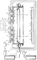
- the invention allows a wide variety of design options; one of them is shown schematically in more detail in the accompanying drawing, which shows the section through a sputtering system with two magnetron sputtering cathodes.
- the drawing shows substrates 1, 1 ', 1' 'which are each to be provided with a thin layer 2, 2', 2 '' made of an oxide (e.g. silicon dioxide or aluminum oxide). These substrates 1, 1 ', 1' 'are opposite targets 3, 3a which are to be atomized. Each target 3, 3a is connected to a cathode body 11, 11a, which receives a magnetic yoke 11b, 11c, which has three magnets 19, 19a, 19b and 19c, 19d, 19e, respectively.
- oxide e.g. silicon dioxide or aluminum oxide
- the polarities of the poles of the six magnets directed at the targets 3, 3a alternate, so that the south poles of the two outer magnets 19, 19b and 19c, 19e with the north pole of the inner magnet 19a and 19d have approximately circular magnetic fields effect through the targets 3, 3a.
- These magnetic fields compress the plasma in front of the targets so that it has its greatest density where the magnetic fields have the maximum of their arcs.
- the ions in the plasma are accelerated by electrical fields that build up due to an alternating voltage that is emitted by the current source 10.
- This AC power source 10 has two terminals 12, 13 that extend from the ends of a secondary transformer winding 25 are formed and are connected to the two cathodes 5, 5a.
- the two current conductors 8, 9 of the secondary transformer winding are connected to the two targets 3, 3a.
- the target 3 is also connected via a line 14 to a voltage-effective value detection 20 connected to earth, which in turn is connected via a further line 21 to a controller 16, which in turn is connected via a line 17 to a control valve 18 which controls the inflow of the Checked reactive gas located in the container 22 in the distribution line 24 of the vacuum chamber 15, 15a.
- the coating chamber 15, 15a is provided with an annular or frame-shaped shielding plate or an aperture 4, which has a gap or slot 6 through which the process gas can flow into the coating chamber 15 from the distributor line 24 in the direction of the arrow.
- the lower edge of the panel 4 is also surrounded by a cooling tube 7, through which a coolant flows and which prevents the panel 4 from overheating.
- the frequency of the alternating current source 10 is set during the sputtering process so that the ions can still follow the alternating field, which is the case at a frequency of approximately 1 kHz to 100 kHz.
- the discharge voltage tapped off via line 14 is fed with the aid of the voltage effective value detection 20 via line 21 as a direct voltage to a controller 16, which in turn controls the solenoid valve 18 for supplying the reactive gas via line 17, in such a way that the measured voltage supplies the required amount of reactive gas certainly.
Landscapes
- Chemical & Material Sciences (AREA)
- Engineering & Computer Science (AREA)
- Chemical Kinetics & Catalysis (AREA)
- Materials Engineering (AREA)
- Mechanical Engineering (AREA)
- Metallurgy (AREA)
- Organic Chemistry (AREA)
- Physics & Mathematics (AREA)
- Plasma & Fusion (AREA)
- Analytical Chemistry (AREA)
- Physical Vapour Deposition (AREA)
Applications Claiming Priority (2)
| Application Number | Priority Date | Filing Date | Title |
|---|---|---|---|
| DE4106770A DE4106770C2 (de) | 1991-03-04 | 1991-03-04 | Verrichtung zum reaktiven Beschichten eines Substrats |
| DE4106770 | 1991-03-04 |
Publications (3)
| Publication Number | Publication Date |
|---|---|
| EP0502242A2 true EP0502242A2 (fr) | 1992-09-09 |
| EP0502242A3 EP0502242A3 (en) | 1993-12-15 |
| EP0502242B1 EP0502242B1 (fr) | 1997-08-27 |
Family
ID=6426380
Family Applications (1)
| Application Number | Title | Priority Date | Filing Date |
|---|---|---|---|
| EP91116294A Expired - Lifetime EP0502242B1 (fr) | 1991-03-04 | 1991-09-25 | Dispositif pour pulverisation réactif |
Country Status (5)
| Country | Link |
|---|---|
| US (1) | US5169509A (fr) |
| EP (1) | EP0502242B1 (fr) |
| JP (1) | JP3363919B2 (fr) |
| KR (1) | KR100239818B1 (fr) |
| DE (2) | DE4106770C2 (fr) |
Cited By (12)
| Publication number | Priority date | Publication date | Assignee | Title |
|---|---|---|---|---|
| WO1995025828A1 (fr) * | 1994-03-19 | 1995-09-28 | Applied Vision Ltd. | Dispositif de revetement de substrat |
| EP0767483A1 (fr) * | 1995-10-06 | 1997-04-09 | Balzers und Leybold Deutschland Holding AG | Dispositif de revêtement de substrats dans le vide |
| EP0782173A2 (fr) * | 1995-10-31 | 1997-07-02 | Balzers und Leybold Deutschland Holding AG | Dispositif pour le revêtement d'un substrat utilisant un procédé de dépÔt chimique en phase vapeur |
| EP0783174A2 (fr) * | 1995-10-27 | 1997-07-09 | Balzers und Leybold Deutschland Holding AG | Dispositif pour le revêtement d'un substrat |
| EP0790326A1 (fr) | 1996-02-17 | 1997-08-20 | Leybold Systems GmbH | Procédé pour déposer une couche optique transparente et électroconductrice sur un substrat d'un matériau transparent |
| WO1997041587A1 (fr) * | 1996-04-29 | 1997-11-06 | Von Ardenne Anlagentechnik Gmbh | Installation a pulverisation cathodique a deux magnetrons longitudinaux |
| WO1998034267A1 (fr) * | 1997-02-01 | 1998-08-06 | Fraunhofer-Gesellschaft zur Förderung der angewandten Forschung e.V. | Procede de regulation de decharges lumineuses a alimentation electrique par impulsions |
| WO1998040530A1 (fr) * | 1997-03-07 | 1998-09-17 | Siemens Aktiengesellschaft | Procede de depot de couches texturees de ysz par pulverisation cathodique |
| EP0636702B1 (fr) * | 1993-07-28 | 1999-05-19 | Asahi Glass Company Ltd. | Procédé pour la formation de films fonctionnels |
| DE19756162A1 (de) * | 1997-12-17 | 1999-07-01 | Ardenne Anlagentech Gmbh | Sputtereinrichtung |
| DE19827587A1 (de) * | 1998-06-20 | 1999-12-23 | Ardenne Anlagentech Gmbh | Einrichtung zur plasmagestützten Schichtabscheidung |
| DE19919742A1 (de) * | 1999-04-30 | 2000-11-02 | Fraunhofer Ges Forschung | Verfahren zum Beschichten von Substraten aus dotiertem Silizium mit einer Antireflexschicht für Solarzellen mittels einer in einer Vakuumkammer betriebenen Zerstäubungskathode mit einem Magnetsystem |
Families Citing this family (88)
| Publication number | Priority date | Publication date | Assignee | Title |
|---|---|---|---|---|
| JPH05148634A (ja) * | 1991-11-22 | 1993-06-15 | Nec Corp | スパツタリング装置 |
| US5415757A (en) * | 1991-11-26 | 1995-05-16 | Leybold Aktiengesellschaft | Apparatus for coating a substrate with electrically nonconductive coatings |
| DE4138793C2 (de) * | 1991-11-26 | 2001-03-01 | Leybold Ag | Verfahren und Vorrichtung zum Beschichten eines Substrats, insbesondere mit elektrisch nichtleitenden Schichten |
| DE4237517A1 (de) * | 1992-11-06 | 1994-05-11 | Leybold Ag | Vorrichtung zum Beschichten eines Substrats, insbesondere mit elektrisch nichtleitenden Schichten |
| CH686747A5 (de) | 1993-04-01 | 1996-06-14 | Balzers Hochvakuum | Optisches Schichtmaterial. |
| DE4311360C2 (de) * | 1993-04-06 | 2002-10-24 | Applied Films Gmbh & Co Kg | Anordnung zum reaktiven Abscheiden von Werkstoffen als Dünnfilm durch Mittelfrequenz-Kathodenzerstäubung |
| US5346601A (en) * | 1993-05-11 | 1994-09-13 | Andrew Barada | Sputter coating collimator with integral reactive gas distribution |
| US6605198B1 (en) * | 1993-07-22 | 2003-08-12 | Sputtered Films, Inc. | Apparatus for, and method of, depositing a film on a substrate |
| DE4326100B4 (de) * | 1993-08-04 | 2006-03-23 | Unaxis Deutschland Holding Gmbh | Verfahren und Vorrichtung zum Beschichten von Substraten in einer Vakuumkammer, mit einer Einrichtung zur Erkennung und Unterdrückung von unerwünschten Lichtbögen |
| US5698082A (en) * | 1993-08-04 | 1997-12-16 | Balzers Und Leybold | Method and apparatus for coating substrates in a vacuum chamber, with a system for the detection and suppression of undesirable arcing |
| IL108677A (en) * | 1994-02-17 | 1997-11-20 | Thin Films Ltd | Sputtering method and apparatus for depositing a coating onto a substrate |
| DE4413655A1 (de) * | 1994-04-20 | 1995-10-26 | Leybold Ag | Beschichtungsanlage |
| US6033483A (en) * | 1994-06-30 | 2000-03-07 | Applied Materials, Inc. | Electrically insulating sealing structure and its method of use in a high vacuum physical vapor deposition apparatus |
| DE4438463C1 (de) * | 1994-10-27 | 1996-02-15 | Fraunhofer Ges Forschung | Verfahren und Schaltung zur bipolaren pulsförmigen Energieeinspeisung in Niederdruckplasmen |
| DE19506515C1 (de) * | 1995-02-24 | 1996-03-07 | Fraunhofer Ges Forschung | Verfahren zur reaktiven Beschichtung |
| DE19508406A1 (de) * | 1995-03-09 | 1996-09-12 | Leybold Ag | Kathodenanordnung für eine Vorrichtung zum Zerstäuben eines Target-Paares |
| US5849162A (en) * | 1995-04-25 | 1998-12-15 | Deposition Sciences, Inc. | Sputtering device and method for reactive for reactive sputtering |
| CA2218279A1 (fr) * | 1995-04-25 | 1996-10-31 | The Boc Group, Inc. | Systeme de pulverisation au moyen de magnetrons cylindriques rotatifs alimentes par courant alternatif |
| US5812405A (en) * | 1995-05-23 | 1998-09-22 | Viratec Thin Films, Inc. | Three variable optimization system for thin film coating design |
| DE19540794A1 (de) | 1995-11-02 | 1997-05-07 | Leybold Ag | Vorrichtung zum Beschichten eines Substrats von einem elektrisch leitfähigen Target |
| DE19604454A1 (de) * | 1996-02-08 | 1997-08-14 | Balzers Prozes System Gmbh | Vorrichtung zum Beschichten von flachen Substraten mit zwei Sputterkathoden |
| US6013155A (en) * | 1996-06-28 | 2000-01-11 | Lam Research Corporation | Gas injection system for plasma processing |
| WO1998000576A1 (fr) | 1996-06-28 | 1998-01-08 | Lam Research Corporation | Appareil et procede pour le depot en phase vapeur par procede chimique au plasma haute densite |
| TW335504B (en) * | 1996-07-09 | 1998-07-01 | Applied Materials Inc | A method for providing full-face high density plasma deposition |
| DE19644752A1 (de) * | 1996-10-28 | 1998-04-30 | Leybold Systems Gmbh | Interferenzschichtensystem |
| DE19651378A1 (de) * | 1996-12-11 | 1998-06-18 | Leybold Systems Gmbh | Vorrichtung zum Aufstäuben von dünnen Schichten auf flache Substrate |
| US6184158B1 (en) | 1996-12-23 | 2001-02-06 | Lam Research Corporation | Inductively coupled plasma CVD |
| DE19715647C2 (de) * | 1997-04-15 | 2001-03-08 | Ardenne Anlagentech Gmbh | Verfahren und Vorrichtung zur Regelung der reaktiven Schichtabscheidung auf Substraten mittels längserstreckten Magnetrons |
| US6217720B1 (en) * | 1997-06-03 | 2001-04-17 | National Research Council Of Canada | Multi-layer reactive sputtering method with reduced stabilization time |
| DE19726966C1 (de) | 1997-06-25 | 1999-01-28 | Flachglas Ag | Verfahren zur Herstellung einer transparenten Silberschicht mit hoher spezifischer elektrischer Leitfähigkeit , Glasscheibe mit einem Dünnschichtsystem mit einer solchen Silberschicht und deren Verwendung |
| US6042687A (en) * | 1997-06-30 | 2000-03-28 | Lam Research Corporation | Method and apparatus for improving etch and deposition uniformity in plasma semiconductor processing |
| EP0896481B1 (fr) * | 1997-08-05 | 2006-08-23 | Micronas Semiconductor Holding AG | Filtre adaptatif |
| DE19740793C2 (de) | 1997-09-17 | 2003-03-20 | Bosch Gmbh Robert | Verfahren zur Beschichtung von Oberflächen mittels einer Anlage mit Sputterelektroden und Verwendung des Verfahrens |
| DE29717418U1 (de) * | 1997-09-26 | 1998-01-22 | Leybold Systems GmbH, 63450 Hanau | Vorrichtung zum Aufbringen dünner Schichten auf ein Substrat |
| US5976334A (en) * | 1997-11-25 | 1999-11-02 | Applied Materials, Inc. | Reliable sustained self-sputtering |
| DE19825056C1 (de) * | 1998-06-04 | 2000-01-13 | Fraunhofer Ges Forschung | Schaltungsanordnung und Verfahren zum Einspeisen von Elektroenergie in ein Plasma |
| JP2000017457A (ja) * | 1998-07-03 | 2000-01-18 | Shincron:Kk | 薄膜形成装置および薄膜形成方法 |
| US6365010B1 (en) | 1998-11-06 | 2002-04-02 | Scivac | Sputtering apparatus and process for high rate coatings |
| US6488824B1 (en) | 1998-11-06 | 2002-12-03 | Raycom Technologies, Inc. | Sputtering apparatus and process for high rate coatings |
| US6499425B1 (en) * | 1999-01-22 | 2002-12-31 | Micron Technology, Inc. | Quasi-remote plasma processing method and apparatus |
| JP2001003166A (ja) * | 1999-04-23 | 2001-01-09 | Nippon Sheet Glass Co Ltd | 基体表面に被膜を被覆する方法およびその方法による基体 |
| US6537428B1 (en) * | 1999-09-02 | 2003-03-25 | Veeco Instruments, Inc. | Stable high rate reactive sputtering |
| US6258217B1 (en) * | 1999-09-29 | 2001-07-10 | Plasma-Therm, Inc. | Rotating magnet array and sputter source |
| DE10015244C2 (de) * | 2000-03-28 | 2002-09-19 | Fraunhofer Ges Forschung | Verfahren und Schaltungsanordnung zur pulsförmigen Energieeinspeisung in Magnetronentladungen |
| US6733642B2 (en) | 2001-04-30 | 2004-05-11 | David A. Glocker | System for unbalanced magnetron sputtering with AC power |
| DE10122431A1 (de) * | 2001-05-09 | 2002-11-28 | Fraunhofer Ges Forschung | Elektrodenanordnung für die magnetfeldgeführte plasmagestützte Abscheidung dünner Schichten im Vakuum |
| DE10154229B4 (de) | 2001-11-07 | 2004-08-05 | Applied Films Gmbh & Co. Kg | Einrichtung für die Regelung einer Plasmaimpedanz |
| US20040149575A1 (en) * | 2002-04-29 | 2004-08-05 | Isoflux, Inc. | System for unbalanced magnetron sputtering with AC power |
| JP3866615B2 (ja) | 2002-05-29 | 2007-01-10 | 株式会社神戸製鋼所 | 反応性スパッタリング方法及び装置 |
| DE10224128A1 (de) * | 2002-05-29 | 2003-12-18 | Schmid Rhyner Ag Adliswil | Verfahren zum Auftrag von Beschichtungen auf Oberflächen |
| US7967957B2 (en) | 2002-08-09 | 2011-06-28 | Kobe Steel, Ltd. | Method for preparing alumna coating film having alpha-type crystal structure as primary structure |
| US20040182701A1 (en) * | 2003-01-29 | 2004-09-23 | Aashi Glass Company, Limited | Sputtering apparatus, a mixed film produced by the sputtering apparatus and a multilayer film including the mixed film |
| DE10306347A1 (de) * | 2003-02-15 | 2004-08-26 | Hüttinger Elektronik GmbH & Co. KG | Leistungszufuhrregeleinheit |
| DE10323258A1 (de) | 2003-05-23 | 2004-12-23 | Applied Films Gmbh & Co. Kg | Magnetron-Sputter-Kathode |
| JP4904165B2 (ja) * | 2004-01-15 | 2012-03-28 | デポジッション サイエンス インク | 堆積工程中に薄膜の光学的特性を監視する方法および装置 |
| DE102004014855A1 (de) * | 2004-03-26 | 2004-10-21 | Applied Films Gmbh & Co. Kg | Einrichtung zum reaktiven Sputtern |
| US20050224343A1 (en) * | 2004-04-08 | 2005-10-13 | Richard Newcomb | Power coupling for high-power sputtering |
| JP2006045611A (ja) * | 2004-08-04 | 2006-02-16 | Nippon Telegr & Teleph Corp <Ntt> | スパッタ成膜装置 |
| US20060065524A1 (en) * | 2004-09-30 | 2006-03-30 | Richard Newcomb | Non-bonded rotatable targets for sputtering |
| CN101044586B (zh) * | 2004-10-18 | 2010-06-16 | 贝卡尔特先进涂层公司 | 一种用于可转动靶材溅射设备的端块 |
| US20060096855A1 (en) * | 2004-11-05 | 2006-05-11 | Richard Newcomb | Cathode arrangement for atomizing a rotatable target pipe |
| US20060278521A1 (en) * | 2005-06-14 | 2006-12-14 | Stowell Michael W | System and method for controlling ion density and energy using modulated power signals |
| US20060278524A1 (en) * | 2005-06-14 | 2006-12-14 | Stowell Michael W | System and method for modulating power signals to control sputtering |
| US7842355B2 (en) * | 2005-11-01 | 2010-11-30 | Applied Materials, Inc. | System and method for modulation of power and power related functions of PECVD discharge sources to achieve new film properties |
| US20070095281A1 (en) * | 2005-11-01 | 2007-05-03 | Stowell Michael W | System and method for power function ramping of microwave liner discharge sources |
| EP1978127A4 (fr) * | 2006-01-25 | 2012-06-20 | Ulvac Inc | Dispositif de projection et procede de formation de film |
| US20100140083A1 (en) * | 2006-10-26 | 2010-06-10 | Hauzer Techno Coating Bv | Dual Magnetron Sputtering Power Supply And Magnetron Sputtering Apparatus |
| WO2009052874A1 (fr) * | 2007-10-26 | 2009-04-30 | Hauzer Techno Coating Bv | Alimentation électrique de pulvérisation à double magnétron et appareil de pulvérisation à magnétron |
| US8137463B2 (en) * | 2007-12-19 | 2012-03-20 | Applied Materials, Inc. | Dual zone gas injection nozzle |
| US8182662B2 (en) * | 2009-03-27 | 2012-05-22 | Sputtering Components, Inc. | Rotary cathode for magnetron sputtering apparatus |
| KR20120014571A (ko) | 2009-04-27 | 2012-02-17 | 오씨 외를리콘 발처스 악티엔게젤샤프트 | 복수의 스퍼터 소스를 구비한 반응성 스퍼터링 |
| DE102009041184A1 (de) * | 2009-09-14 | 2011-09-15 | Solarworld Innovations Gmbh | Beschichtungs-Vorrichtung und -Verfahren |
| KR20130041105A (ko) * | 2010-06-17 | 2013-04-24 | 울박, 인크 | 스퍼터 성막 장치 및 방착부재 |
| JP5743266B2 (ja) * | 2010-08-06 | 2015-07-01 | キヤノンアネルバ株式会社 | 成膜装置及びキャリブレーション方法 |
| JP5256475B2 (ja) * | 2011-02-10 | 2013-08-07 | 株式会社ユーテック | 対向ターゲット式スパッタ装置及び対向ターゲット式スパッタ方法 |
| US9941100B2 (en) | 2011-12-16 | 2018-04-10 | Taiwan Semiconductor Manufacturing Company, Ltd. | Adjustable nozzle for plasma deposition and a method of controlling the adjustable nozzle |
| US9790596B1 (en) * | 2013-01-30 | 2017-10-17 | Kyocera Corporation | Gas nozzle and plasma device employing same |
| JP6101533B2 (ja) * | 2013-03-27 | 2017-03-22 | 株式会社Screenホールディングス | 酸化アルミニウムの成膜方法 |
| CN105555990B (zh) | 2013-07-17 | 2018-01-09 | 先进能源工业公司 | 在脉冲双磁控管溅射(dms)工艺中平衡靶消耗的系统和方法 |
| US10465288B2 (en) * | 2014-08-15 | 2019-11-05 | Applied Materials, Inc. | Nozzle for uniform plasma processing |
| US10208380B2 (en) * | 2015-12-04 | 2019-02-19 | Applied Materials, Inc. | Advanced coating method and materials to prevent HDP-CVD chamber arcing |
| KR102553629B1 (ko) * | 2016-06-17 | 2023-07-11 | 삼성전자주식회사 | 플라즈마 처리 장치 |
| DE102016118799B4 (de) | 2016-10-05 | 2022-08-11 | VON ARDENNE Asset GmbH & Co. KG | Verfahren zum Magnetronsputtern |
| WO2019004192A1 (fr) * | 2017-06-27 | 2019-01-03 | キヤノンアネルバ株式会社 | Dispositif de traitement par plasma |
| EP3648550B1 (fr) | 2017-06-27 | 2021-06-02 | Canon Anelva Corporation | Dispositif de traitement au plasma |
| PL3648551T3 (pl) | 2017-06-27 | 2021-12-06 | Canon Anelva Corporation | Urządzenie do obróbki plazmowej |
| KR102257134B1 (ko) | 2017-06-27 | 2021-05-26 | 캐논 아네르바 가부시키가이샤 | 플라스마 처리 장치 |
| KR102439024B1 (ko) | 2018-06-26 | 2022-09-02 | 캐논 아네르바 가부시키가이샤 | 플라스마 처리 장치, 플라스마 처리 방법, 프로그램, 및 메모리 매체 |
Citations (5)
| Publication number | Priority date | Publication date | Assignee | Title |
|---|---|---|---|---|
| GB1172106A (en) * | 1967-06-29 | 1969-11-26 | Edwards High Vacuum Int Ltd | Improvements in or relating to Pressure Control in Vacuum Apparatus |
| US4166784A (en) * | 1978-04-28 | 1979-09-04 | Applied Films Lab, Inc. | Feedback control for vacuum deposition apparatus |
| DD252205A1 (de) * | 1986-09-01 | 1987-12-09 | Ardenne Forschungsinst | Zerstaeubungseinrichtung |
| DE3802852A1 (de) * | 1988-02-01 | 1989-08-03 | Leybold Ag | Einrichtung fuer die beschichtung eines substrats mit einem material, das aus einem plasma gewonnen wird |
| EP0411359A2 (fr) * | 1989-08-02 | 1991-02-06 | Leybold Aktiengesellschaft | Dispositif pour mesurer l'épaisseur de fines couches |
Family Cites Families (5)
| Publication number | Priority date | Publication date | Assignee | Title |
|---|---|---|---|---|
| FR95311E (fr) * | 1967-03-24 | 1970-08-21 | Varian Associates | Appareil de pulvérisation cathodique pour déposer des pellicules minces sur des surfaces a revetir. |
| US3860507A (en) * | 1972-11-29 | 1975-01-14 | Rca Corp | Rf sputtering apparatus and method |
| JPS61179864A (ja) * | 1985-02-06 | 1986-08-12 | Hitachi Ltd | スパツタ装置 |
| US4738761A (en) * | 1986-10-06 | 1988-04-19 | Microelectronics Center Of North Carolina | Shared current loop, multiple field apparatus and process for plasma processing |
| JPH01268869A (ja) * | 1988-04-20 | 1989-10-26 | Fuji Photo Film Co Ltd | スパッタリング装置 |
-
1991
- 1991-03-04 DE DE4106770A patent/DE4106770C2/de not_active Expired - Lifetime
- 1991-05-09 US US07/697,712 patent/US5169509A/en not_active Expired - Lifetime
- 1991-09-25 EP EP91116294A patent/EP0502242B1/fr not_active Expired - Lifetime
- 1991-09-25 DE DE59108836T patent/DE59108836D1/de not_active Expired - Lifetime
- 1991-10-14 KR KR1019910018055A patent/KR100239818B1/ko not_active IP Right Cessation
-
1992
- 1992-03-03 JP JP04517592A patent/JP3363919B2/ja not_active Expired - Lifetime
Patent Citations (5)
| Publication number | Priority date | Publication date | Assignee | Title |
|---|---|---|---|---|
| GB1172106A (en) * | 1967-06-29 | 1969-11-26 | Edwards High Vacuum Int Ltd | Improvements in or relating to Pressure Control in Vacuum Apparatus |
| US4166784A (en) * | 1978-04-28 | 1979-09-04 | Applied Films Lab, Inc. | Feedback control for vacuum deposition apparatus |
| DD252205A1 (de) * | 1986-09-01 | 1987-12-09 | Ardenne Forschungsinst | Zerstaeubungseinrichtung |
| DE3802852A1 (de) * | 1988-02-01 | 1989-08-03 | Leybold Ag | Einrichtung fuer die beschichtung eines substrats mit einem material, das aus einem plasma gewonnen wird |
| EP0411359A2 (fr) * | 1989-08-02 | 1991-02-06 | Leybold Aktiengesellschaft | Dispositif pour mesurer l'épaisseur de fines couches |
Cited By (19)
| Publication number | Priority date | Publication date | Assignee | Title |
|---|---|---|---|---|
| US6468403B1 (en) | 1993-07-28 | 2002-10-22 | Asahi Glass Company Ltd. | Methods for producing functional films |
| EP0636702B1 (fr) * | 1993-07-28 | 1999-05-19 | Asahi Glass Company Ltd. | Procédé pour la formation de films fonctionnels |
| WO1995025828A1 (fr) * | 1994-03-19 | 1995-09-28 | Applied Vision Ltd. | Dispositif de revetement de substrat |
| EP0767483A1 (fr) * | 1995-10-06 | 1997-04-09 | Balzers und Leybold Deutschland Holding AG | Dispositif de revêtement de substrats dans le vide |
| EP0783174A3 (fr) * | 1995-10-27 | 1999-02-17 | Balzers und Leybold Deutschland Holding AG | Dispositif pour le revêtement d'un substrat |
| US6168698B1 (en) | 1995-10-27 | 2001-01-02 | Balzers Und Leybold Deutschland Holding Ag | Apparatus for coating a substrate |
| EP0783174A2 (fr) * | 1995-10-27 | 1997-07-09 | Balzers und Leybold Deutschland Holding AG | Dispositif pour le revêtement d'un substrat |
| EP0782173A3 (fr) * | 1995-10-31 | 1999-02-17 | Balzers und Leybold Deutschland Holding AG | Dispositif pour le revêtement d'un substrat utilisant un procédé de dépÔt chimique en phase vapeur |
| EP0782173A2 (fr) * | 1995-10-31 | 1997-07-02 | Balzers und Leybold Deutschland Holding AG | Dispositif pour le revêtement d'un substrat utilisant un procédé de dépÔt chimique en phase vapeur |
| DE19605932A1 (de) * | 1996-02-17 | 1997-08-21 | Leybold Systems Gmbh | Verfahren zum Ablagern einer optisch transparenten und elektrisch leitenden Schicht auf einem Substrat aus durchscheinendem Werkstoff |
| EP0790326A1 (fr) | 1996-02-17 | 1997-08-20 | Leybold Systems GmbH | Procédé pour déposer une couche optique transparente et électroconductrice sur un substrat d'un matériau transparent |
| WO1997041587A1 (fr) * | 1996-04-29 | 1997-11-06 | Von Ardenne Anlagentechnik Gmbh | Installation a pulverisation cathodique a deux magnetrons longitudinaux |
| US6361668B1 (en) | 1996-04-29 | 2002-03-26 | Von Ardenne Anlagentechnik Gmbh | Sputtering installation with two longitudinally placed magnetrons |
| WO1998034267A1 (fr) * | 1997-02-01 | 1998-08-06 | Fraunhofer-Gesellschaft zur Förderung der angewandten Forschung e.V. | Procede de regulation de decharges lumineuses a alimentation electrique par impulsions |
| WO1998040530A1 (fr) * | 1997-03-07 | 1998-09-17 | Siemens Aktiengesellschaft | Procede de depot de couches texturees de ysz par pulverisation cathodique |
| DE19756162C2 (de) * | 1997-12-17 | 1999-10-14 | Ardenne Anlagentech Gmbh | Sputtereinrichtung |
| DE19756162A1 (de) * | 1997-12-17 | 1999-07-01 | Ardenne Anlagentech Gmbh | Sputtereinrichtung |
| DE19827587A1 (de) * | 1998-06-20 | 1999-12-23 | Ardenne Anlagentech Gmbh | Einrichtung zur plasmagestützten Schichtabscheidung |
| DE19919742A1 (de) * | 1999-04-30 | 2000-11-02 | Fraunhofer Ges Forschung | Verfahren zum Beschichten von Substraten aus dotiertem Silizium mit einer Antireflexschicht für Solarzellen mittels einer in einer Vakuumkammer betriebenen Zerstäubungskathode mit einem Magnetsystem |
Also Published As
| Publication number | Publication date |
|---|---|
| US5169509A (en) | 1992-12-08 |
| EP0502242B1 (fr) | 1997-08-27 |
| KR100239818B1 (ko) | 2000-01-15 |
| KR930008185A (ko) | 1993-05-21 |
| DE4106770C2 (de) | 1996-10-17 |
| JP3363919B2 (ja) | 2003-01-08 |
| DE4106770A1 (de) | 1992-09-10 |
| JPH04325680A (ja) | 1992-11-16 |
| EP0502242A3 (en) | 1993-12-15 |
| DE59108836D1 (de) | 1997-10-02 |
Similar Documents
| Publication | Publication Date | Title |
|---|---|---|
| EP0502242B1 (fr) | Dispositif pour pulverisation réactif | |
| DE4042287C2 (de) | Vorrichtung zum reaktiven Aufstäuben von elektrisch isolierendem Werkstoff | |
| EP0416241B1 (fr) | Dispositif pour le revêtement d'un substrat | |
| EP0958195B1 (fr) | Procede de revetement de surfaces au moyen d'une installation dotee d'electrodes de depot par pulverisation | |
| EP0782173A2 (fr) | Dispositif pour le revêtement d'un substrat utilisant un procédé de dépÔt chimique en phase vapeur | |
| EP0755461A1 (fr) | Procede et dispositif de revetement par evaporation sous vide par voie ionique | |
| DE4042288A1 (de) | Verfahren und vorrichtung zum reaktiven beschichten eines substrats | |
| DE2513216B2 (de) | Verfahren und Vorrichtung zur Beschichtung eines Substrats durch reaktive Kathodenzerstäubung | |
| DE69329161T2 (de) | Verbesserungen von Verfahren der physikalischen Dampfphasen-Abscheidung | |
| DE4237517A1 (de) | Vorrichtung zum Beschichten eines Substrats, insbesondere mit elektrisch nichtleitenden Schichten | |
| DE19651811A1 (de) | Vorrichtung zum Belegen eines Substrats mit dünnen Schichten | |
| DE4042289A1 (de) | Verfahren und vorrichtung zum reaktiven beschichten eines substrats | |
| EP0422323B1 (fr) | Utilisation d'helium comme gaz pour revêtir un substrat de polyméthylméthacrylate avec une couche mince de l'aluminium | |
| EP0772223B1 (fr) | Dispositif pour revêtir un substrat à partir de cibles conductrices d'électricité | |
| WO2011160766A1 (fr) | Source d'évaporation par arc présentant un champ électrique défini | |
| EP0767483B1 (fr) | Dispositif de revêtement de substrats dans le vide | |
| DE4239218C2 (de) | Anordnung zum Verhindern von Überschlägen in einem Plasma-Prozeßraum | |
| WO1996026533A1 (fr) | Dispositif de pulverisation reactive | |
| DE3880275T2 (de) | Anlage und Verfahren zur Ablagerung einer dünnen Schicht auf ein durchsichtiges Substrat, insbesondere zur Herstellung von Glasscheiben. | |
| DE4136655C2 (de) | Vorrichtung zum reaktiven Beschichten eines Substrats | |
| DE69403538T2 (de) | Vorrichtung zur reaktiven Plasmagasphasenabscheidung eines elektrisch nichtleitenden Materials unter Verwendung einer abgeschirmten Sekundäranode | |
| EP0776987B1 (fr) | Appareillage de revêtement sous vide avec un creuset pour recevoir le matériau à évaporer dans la chambre à vide | |
| DE4138793C2 (de) | Verfahren und Vorrichtung zum Beschichten eines Substrats, insbesondere mit elektrisch nichtleitenden Schichten | |
| DE19605932A1 (de) | Verfahren zum Ablagern einer optisch transparenten und elektrisch leitenden Schicht auf einem Substrat aus durchscheinendem Werkstoff | |
| DE102009018912A1 (de) | Verfahren zur Erzeugung eines Plasmastrahls sowie Plasmaquelle |
Legal Events
| Date | Code | Title | Description |
|---|---|---|---|
| PUAI | Public reference made under article 153(3) epc to a published international application that has entered the european phase |
Free format text: ORIGINAL CODE: 0009012 |
|
| AK | Designated contracting states |
Kind code of ref document: A2 Designated state(s): CH DE FR GB LI NL |
|
| 17P | Request for examination filed |
Effective date: 19920818 |
|
| PUAL | Search report despatched |
Free format text: ORIGINAL CODE: 0009013 |
|
| AK | Designated contracting states |
Kind code of ref document: A3 Designated state(s): CH DE FR GB LI NL |
|
| 17Q | First examination report despatched |
Effective date: 19950313 |
|
| RAP1 | Party data changed (applicant data changed or rights of an application transferred) |
Owner name: BALZERS UND LEYBOLD DEUTSCHLAND HOLDING AKTIENGESE |
|
| GRAG | Despatch of communication of intention to grant |
Free format text: ORIGINAL CODE: EPIDOS AGRA |
|
| GRAH | Despatch of communication of intention to grant a patent |
Free format text: ORIGINAL CODE: EPIDOS IGRA |
|
| GRAH | Despatch of communication of intention to grant a patent |
Free format text: ORIGINAL CODE: EPIDOS IGRA |
|
| GRAA | (expected) grant |
Free format text: ORIGINAL CODE: 0009210 |
|
| AK | Designated contracting states |
Kind code of ref document: B1 Designated state(s): CH DE FR GB LI NL |
|
| REG | Reference to a national code |
Ref country code: CH Ref legal event code: NV Representative=s name: PATENTANWALTSBUERO FELDMANN AG Ref country code: CH Ref legal event code: EP |
|
| GBT | Gb: translation of ep patent filed (gb section 77(6)(a)/1977) |
Effective date: 19970901 |
|
| REF | Corresponds to: |
Ref document number: 59108836 Country of ref document: DE Date of ref document: 19971002 |
|
| ET | Fr: translation filed | ||
| PLBE | No opposition filed within time limit |
Free format text: ORIGINAL CODE: 0009261 |
|
| STAA | Information on the status of an ep patent application or granted ep patent |
Free format text: STATUS: NO OPPOSITION FILED WITHIN TIME LIMIT |
|
| 26N | No opposition filed | ||
| REG | Reference to a national code |
Ref country code: GB Ref legal event code: IF02 |
|
| REG | Reference to a national code |
Ref country code: CH Ref legal event code: PFA Owner name: BALZERS UND LEYBOLD DEUTSCHLAND HOLDING AKTIENGES Free format text: BALZERS UND LEYBOLD DEUTSCHLAND HOLDING AKTIENGESELLSCHAFT#WILHELM-ROHN-STRASSE 25#63450 HANAU (DE) -TRANSFER TO- BALZERS UND LEYBOLD DEUTSCHLAND HOLDING AKTIENGESELLSCHAFT#WILHELM-ROHN-STRASSE 25#63450 HANAU (DE) |
|
| PGFP | Annual fee paid to national office [announced via postgrant information from national office to epo] |
Ref country code: CH Payment date: 20100923 Year of fee payment: 20 |
|
| PGFP | Annual fee paid to national office [announced via postgrant information from national office to epo] |
Ref country code: FR Payment date: 20101005 Year of fee payment: 20 |
|
| PGFP | Annual fee paid to national office [announced via postgrant information from national office to epo] |
Ref country code: GB Payment date: 20100921 Year of fee payment: 20 |
|
| PGFP | Annual fee paid to national office [announced via postgrant information from national office to epo] |
Ref country code: NL Payment date: 20100916 Year of fee payment: 20 |
|
| PGFP | Annual fee paid to national office [announced via postgrant information from national office to epo] |
Ref country code: DE Payment date: 20100922 Year of fee payment: 20 |
|
| REG | Reference to a national code |
Ref country code: DE Ref legal event code: R071 Ref document number: 59108836 Country of ref document: DE |
|
| REG | Reference to a national code |
Ref country code: DE Ref legal event code: R071 Ref document number: 59108836 Country of ref document: DE |
|
| REG | Reference to a national code |
Ref country code: CH Ref legal event code: PL |
|
| REG | Reference to a national code |
Ref country code: NL Ref legal event code: V4 Effective date: 20110925 |
|
| REG | Reference to a national code |
Ref country code: GB Ref legal event code: PE20 Expiry date: 20110924 |
|
| PG25 | Lapsed in a contracting state [announced via postgrant information from national office to epo] |
Ref country code: GB Free format text: LAPSE BECAUSE OF EXPIRATION OF PROTECTION Effective date: 20110924 |
|
| PG25 | Lapsed in a contracting state [announced via postgrant information from national office to epo] |
Ref country code: NL Free format text: LAPSE BECAUSE OF EXPIRATION OF PROTECTION Effective date: 20110925 |
|
| PG25 | Lapsed in a contracting state [announced via postgrant information from national office to epo] |
Ref country code: DE Free format text: LAPSE BECAUSE OF EXPIRATION OF PROTECTION Effective date: 20110926 |