EP0502242A2 - Process and apparatus for reactive coating of a substrate - Google Patents
Process and apparatus for reactive coating of a substrate Download PDFInfo
- Publication number
- EP0502242A2 EP0502242A2 EP91116294A EP91116294A EP0502242A2 EP 0502242 A2 EP0502242 A2 EP 0502242A2 EP 91116294 A EP91116294 A EP 91116294A EP 91116294 A EP91116294 A EP 91116294A EP 0502242 A2 EP0502242 A2 EP 0502242A2
- Authority
- EP
- European Patent Office
- Prior art keywords
- cathodes
- voltage
- substrate
- coating chamber
- targets
- Prior art date
- Legal status (The legal status is an assumption and is not a legal conclusion. Google has not performed a legal analysis and makes no representation as to the accuracy of the status listed.)
- Granted
Links
Images
Classifications
-
- C—CHEMISTRY; METALLURGY
- C23—COATING METALLIC MATERIAL; COATING MATERIAL WITH METALLIC MATERIAL; CHEMICAL SURFACE TREATMENT; DIFFUSION TREATMENT OF METALLIC MATERIAL; COATING BY VACUUM EVAPORATION, BY SPUTTERING, BY ION IMPLANTATION OR BY CHEMICAL VAPOUR DEPOSITION, IN GENERAL; INHIBITING CORROSION OF METALLIC MATERIAL OR INCRUSTATION IN GENERAL
- C23C—COATING METALLIC MATERIAL; COATING MATERIAL WITH METALLIC MATERIAL; SURFACE TREATMENT OF METALLIC MATERIAL BY DIFFUSION INTO THE SURFACE, BY CHEMICAL CONVERSION OR SUBSTITUTION; COATING BY VACUUM EVAPORATION, BY SPUTTERING, BY ION IMPLANTATION OR BY CHEMICAL VAPOUR DEPOSITION, IN GENERAL
- C23C14/00—Coating by vacuum evaporation, by sputtering or by ion implantation of the coating forming material
- C23C14/22—Coating by vacuum evaporation, by sputtering or by ion implantation of the coating forming material characterised by the process of coating
- C23C14/34—Sputtering
- C23C14/35—Sputtering by application of a magnetic field, e.g. magnetron sputtering
-
- H—ELECTRICITY
- H01—ELECTRIC ELEMENTS
- H01J—ELECTRIC DISCHARGE TUBES OR DISCHARGE LAMPS
- H01J37/00—Discharge tubes with provision for introducing objects or material to be exposed to the discharge, e.g. for the purpose of examination or processing thereof
- H01J37/32—Gas-filled discharge tubes
- H01J37/32431—Constructional details of the reactor
- H01J37/3244—Gas supply means
- H01J37/32449—Gas control, e.g. control of the gas flow
-
- C—CHEMISTRY; METALLURGY
- C23—COATING METALLIC MATERIAL; COATING MATERIAL WITH METALLIC MATERIAL; CHEMICAL SURFACE TREATMENT; DIFFUSION TREATMENT OF METALLIC MATERIAL; COATING BY VACUUM EVAPORATION, BY SPUTTERING, BY ION IMPLANTATION OR BY CHEMICAL VAPOUR DEPOSITION, IN GENERAL; INHIBITING CORROSION OF METALLIC MATERIAL OR INCRUSTATION IN GENERAL
- C23C—COATING METALLIC MATERIAL; COATING MATERIAL WITH METALLIC MATERIAL; SURFACE TREATMENT OF METALLIC MATERIAL BY DIFFUSION INTO THE SURFACE, BY CHEMICAL CONVERSION OR SUBSTITUTION; COATING BY VACUUM EVAPORATION, BY SPUTTERING, BY ION IMPLANTATION OR BY CHEMICAL VAPOUR DEPOSITION, IN GENERAL
- C23C14/00—Coating by vacuum evaporation, by sputtering or by ion implantation of the coating forming material
- C23C14/0021—Reactive sputtering or evaporation
- C23C14/0036—Reactive sputtering
- C23C14/0063—Reactive sputtering characterised by means for introducing or removing gases
-
- C—CHEMISTRY; METALLURGY
- C23—COATING METALLIC MATERIAL; COATING MATERIAL WITH METALLIC MATERIAL; CHEMICAL SURFACE TREATMENT; DIFFUSION TREATMENT OF METALLIC MATERIAL; COATING BY VACUUM EVAPORATION, BY SPUTTERING, BY ION IMPLANTATION OR BY CHEMICAL VAPOUR DEPOSITION, IN GENERAL; INHIBITING CORROSION OF METALLIC MATERIAL OR INCRUSTATION IN GENERAL
- C23C—COATING METALLIC MATERIAL; COATING MATERIAL WITH METALLIC MATERIAL; SURFACE TREATMENT OF METALLIC MATERIAL BY DIFFUSION INTO THE SURFACE, BY CHEMICAL CONVERSION OR SUBSTITUTION; COATING BY VACUUM EVAPORATION, BY SPUTTERING, BY ION IMPLANTATION OR BY CHEMICAL VAPOUR DEPOSITION, IN GENERAL
- C23C14/00—Coating by vacuum evaporation, by sputtering or by ion implantation of the coating forming material
- C23C14/0021—Reactive sputtering or evaporation
- C23C14/0036—Reactive sputtering
- C23C14/0068—Reactive sputtering characterised by means for confinement of gases or sputtered material, e.g. screens, baffles
-
- C—CHEMISTRY; METALLURGY
- C23—COATING METALLIC MATERIAL; COATING MATERIAL WITH METALLIC MATERIAL; CHEMICAL SURFACE TREATMENT; DIFFUSION TREATMENT OF METALLIC MATERIAL; COATING BY VACUUM EVAPORATION, BY SPUTTERING, BY ION IMPLANTATION OR BY CHEMICAL VAPOUR DEPOSITION, IN GENERAL; INHIBITING CORROSION OF METALLIC MATERIAL OR INCRUSTATION IN GENERAL
- C23C—COATING METALLIC MATERIAL; COATING MATERIAL WITH METALLIC MATERIAL; SURFACE TREATMENT OF METALLIC MATERIAL BY DIFFUSION INTO THE SURFACE, BY CHEMICAL CONVERSION OR SUBSTITUTION; COATING BY VACUUM EVAPORATION, BY SPUTTERING, BY ION IMPLANTATION OR BY CHEMICAL VAPOUR DEPOSITION, IN GENERAL
- C23C14/00—Coating by vacuum evaporation, by sputtering or by ion implantation of the coating forming material
- C23C14/22—Coating by vacuum evaporation, by sputtering or by ion implantation of the coating forming material characterised by the process of coating
- C23C14/34—Sputtering
- C23C14/35—Sputtering by application of a magnetic field, e.g. magnetron sputtering
- C23C14/352—Sputtering by application of a magnetic field, e.g. magnetron sputtering using more than one target
-
- H—ELECTRICITY
- H01—ELECTRIC ELEMENTS
- H01J—ELECTRIC DISCHARGE TUBES OR DISCHARGE LAMPS
- H01J37/00—Discharge tubes with provision for introducing objects or material to be exposed to the discharge, e.g. for the purpose of examination or processing thereof
- H01J37/32—Gas-filled discharge tubes
- H01J37/34—Gas-filled discharge tubes operating with cathodic sputtering
- H01J37/3402—Gas-filled discharge tubes operating with cathodic sputtering using supplementary magnetic fields
- H01J37/3405—Magnetron sputtering
- H01J37/3408—Planar magnetron sputtering
-
- H—ELECTRICITY
- H01—ELECTRIC ELEMENTS
- H01J—ELECTRIC DISCHARGE TUBES OR DISCHARGE LAMPS
- H01J37/00—Discharge tubes with provision for introducing objects or material to be exposed to the discharge, e.g. for the purpose of examination or processing thereof
- H01J37/32—Gas-filled discharge tubes
- H01J37/34—Gas-filled discharge tubes operating with cathodic sputtering
- H01J37/3411—Constructional aspects of the reactor
- H01J37/3414—Targets
- H01J37/3426—Material
- H01J37/3429—Plural materials
Definitions
- the invention relates to a device for the reactive coating of a substrate with an electrically insulating material, for example with silicon dioxide (SiO2), consisting of an alternating current source which is connected to an electrode which is arranged in an evacuable coating chamber and which is electrically connected to targets which are atomized and their atomized particles are deposited on the substrate, a process gas and a reactive gas being able to be introduced into the coating chamber.
- an electrically insulating material for example with silicon dioxide (SiO2)
- a sputtering device working with radio frequency - preferably at 13.56 MHz - is already known (US Pat. No. 3,860,507), in which two diametrically opposed targets are provided in the process chamber, each of which is connected via electrodes to the two outputs of the secondary winding of an AC transformer are, wherein the secondary winding has a center tap, which is electrically connected to the wall of the process chamber, such that a glow discharge is formed between the two targets.
- a device for coating a substrate with a material which is obtained from a plasma is known (DE-OS 38 02 852), the substrate being located between a first and a second electrode and in which the first electrode is connected to one first connection of an AC power source and the second electrode is connected to a second connection of the AC power source.
- the alternating current source is designed as a stray field transformer, which is fed from a protective gas welding system or a similar regulated alternating current supply.
- the two electrodes can optionally be connected to a direct current supply.
- a sputtering device consisting of a magnet system and at least two electrodes arranged above it, which consist of the material to be sputtered and are connected so that they are alternately cathode and anode of a gas discharge, the electrodes being connected to one sinusoidal AC voltage of preferably 50 Hz are connected.
- An independent magnet system is assigned to each electrode, a pole of one magnet system being a pole of the adjacent magnet system and the electrodes being arranged in one plane.
- the present invention is therefore based on the object to provide a device for sputtering materials with a high affinity for a reactive gas, which enables a uniform or stable process and works smoothly and in particular without flashing even during long operating times, and this with the deposition of insulating layers, such as e.g. B. SiO2, Al2O3, NiSi2 oxide, ZrO2, TiO2, ZnO, SnO2, Si3N4, these layers should adhere particularly firmly to the substrate.
- insulating layers such as e.g. B. SiO2, Al2O3, NiSi2 oxide, ZrO2, TiO2, ZnO, SnO2, Si3N4, these layers should adhere particularly firmly to the substrate.
- electrodes which are electrically separated from one another and from the sputtering chamber but are arranged next to one another and are designed as magnetron cathodes, in each of which the cathode body and the material of the targets are electrically connected to the floating outputs of an AC power source, for which the power supply has an output has two connections, which are formed, for example, from the two ends of a secondary transformer winding.
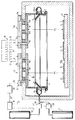
- the invention allows a wide variety of design options; one of them is shown schematically in more detail in the accompanying drawing, which shows the section through a sputtering system with two magnetron sputtering cathodes.
- the drawing shows substrates 1, 1 ', 1' 'which are each to be provided with a thin layer 2, 2', 2 '' made of an oxide (e.g. silicon dioxide or aluminum oxide). These substrates 1, 1 ', 1' 'are opposite targets 3, 3a which are to be atomized. Each target 3, 3a is connected to a cathode body 11, 11a, which receives a magnetic yoke 11b, 11c, which has three magnets 19, 19a, 19b and 19c, 19d, 19e, respectively.
- oxide e.g. silicon dioxide or aluminum oxide
- the polarities of the poles of the six magnets directed at the targets 3, 3a alternate, so that the south poles of the two outer magnets 19, 19b and 19c, 19e with the north pole of the inner magnet 19a and 19d have approximately circular magnetic fields effect through the targets 3, 3a.
- These magnetic fields compress the plasma in front of the targets so that it has its greatest density where the magnetic fields have the maximum of their arcs.
- the ions in the plasma are accelerated by electrical fields that build up due to an alternating voltage that is emitted by the current source 10.
- This AC power source 10 has two terminals 12, 13 that extend from the ends of a secondary transformer winding 25 are formed and are connected to the two cathodes 5, 5a.
- the two current conductors 8, 9 of the secondary transformer winding are connected to the two targets 3, 3a.
- the target 3 is also connected via a line 14 to a voltage-effective value detection 20 connected to earth, which in turn is connected via a further line 21 to a controller 16, which in turn is connected via a line 17 to a control valve 18 which controls the inflow of the Checked reactive gas located in the container 22 in the distribution line 24 of the vacuum chamber 15, 15a.
- the coating chamber 15, 15a is provided with an annular or frame-shaped shielding plate or an aperture 4, which has a gap or slot 6 through which the process gas can flow into the coating chamber 15 from the distributor line 24 in the direction of the arrow.
- the lower edge of the panel 4 is also surrounded by a cooling tube 7, through which a coolant flows and which prevents the panel 4 from overheating.
- the frequency of the alternating current source 10 is set during the sputtering process so that the ions can still follow the alternating field, which is the case at a frequency of approximately 1 kHz to 100 kHz.
- the discharge voltage tapped off via line 14 is fed with the aid of the voltage effective value detection 20 via line 21 as a direct voltage to a controller 16, which in turn controls the solenoid valve 18 for supplying the reactive gas via line 17, in such a way that the measured voltage supplies the required amount of reactive gas certainly.
Landscapes
- Chemical & Material Sciences (AREA)
- Engineering & Computer Science (AREA)
- Chemical Kinetics & Catalysis (AREA)
- Materials Engineering (AREA)
- Mechanical Engineering (AREA)
- Metallurgy (AREA)
- Organic Chemistry (AREA)
- Physics & Mathematics (AREA)
- Plasma & Fusion (AREA)
- Analytical Chemistry (AREA)
- Physical Vapour Deposition (AREA)
Abstract
Description
Die Erfindung betrifft eine Vorrichtung zum reaktiven Beschichten eines Substrats mit einem elektrisch isolierenden Werkstoff, beispielsweise mit Siliziumdioxid (SiO₂), bestehend aus einer Wechselstromquelle, die mit in einer evakuierbaren Beschichtungskammer angeordneten Elektrode verbunden ist, die elektrisch mit Targets in Verbindung steht, die zerstäubt werden und deren zerstäubte Teilchen sich auf dem Substrat niederschlagen, wobei in die Beschichtungskammer ein Prozeßgas und ein Reaktivgas einbringbar sind.The invention relates to a device for the reactive coating of a substrate with an electrically insulating material, for example with silicon dioxide (SiO₂), consisting of an alternating current source which is connected to an electrode which is arranged in an evacuable coating chamber and which is electrically connected to targets which are atomized and their atomized particles are deposited on the substrate, a process gas and a reactive gas being able to be introduced into the coating chamber.
Bei bekannten Verfahren zum Beschichten von Substraten mit Hilfe von Kathodenzerstäubung und Materialien mit einer hohen Affinität zum Reaktivgas besteht das Problem, daß neben dem Substrat selbst auch Teile der Vorrichtung - wie die Innenwand der Prozeßkammer oder Teile von Blenden oder die Targetoberfläche - mit elektrisch nicht- oder schlechtleitenden Materialien beschichtet werden, was die häufige Änderung der Prozeßparameter zur Folge hat und insbesondere auch zu elektrischen Überschlägen führt, so daß eine häufige Unterbrechung des Prozesses und auch eine häufige Reinigung oder ein Austausch von Teilen der Vorrichtung erforderlich wird.In known methods for coating substrates using cathode sputtering and materials with a high affinity for the reactive gas, there is the problem that in addition to the substrate itself, parts of the device - such as the inner wall of the process chamber or parts of diaphragms or the target surface - are coated with electrically non-conductive or poorly conductive materials, which results in frequent changes in the process parameters and in particular also leads to electrical flashovers, so that frequent interruption of the process and also frequent cleaning or replacement of parts of the device is required.
Es ist bereits eine mit Radiofrequenz - vorzugsweise mit 13,56 MHz - arbeitende Sputtervorrichtung bekannt (US-PS 3,860,507), bei der in der Prozeßkammer zwei einander diametral gegenüberliegende Targets vorgesehen sind, die jeweils über Elektroden mit den beiden Ausgängen der Sekundärwicklung eines Wechselstromtransformators verbunden sind, wobei die Sekundärwicklung eine Mittenanzapfung aufweist, die elektrisch an die Wandung der Prozeßkammer angeschlossen ist, derart, daß sich zwischen den beiden Targets eine Glimmentladung ausbildet.A sputtering device working with radio frequency - preferably at 13.56 MHz - is already known (US Pat. No. 3,860,507), in which two diametrically opposed targets are provided in the process chamber, each of which is connected via electrodes to the two outputs of the secondary winding of an AC transformer are, wherein the secondary winding has a center tap, which is electrically connected to the wall of the process chamber, such that a glow discharge is formed between the two targets.
Weiterhin ist eine Einrichtung für die Beschichtung eines Substrats mit einem Material, das aus einem Plasma gewonnen wird, bekannt (DE-OS 38 02 852), wobei sich das Substrat zwischen einer ersten und einer zweiten Elektrode befindet und bei der die erste Elektrode an einem ersten Anschluß einer Wechselstromquelle und die zweite Elektrode an einem zweiten Anschluß der Wechselstromquelle liegt. Die Wechselstromquelle ist in diesem Falle als Streufeldtransformator ausgebildet, der aus einer Schutzgasschweißanlage oder einer ähnlichen geregelten Wechselstromversorgung gespeist wird. Darüberhinaus sind die beiden Elektroden wahlweise auch mit einer Gleichstromversorgung verbindbar.Furthermore, a device for coating a substrate with a material which is obtained from a plasma is known (DE-OS 38 02 852), the substrate being located between a first and a second electrode and in which the first electrode is connected to one first connection of an AC power source and the second electrode is connected to a second connection of the AC power source. In this case, the alternating current source is designed as a stray field transformer, which is fed from a protective gas welding system or a similar regulated alternating current supply. In addition, the two electrodes can optionally be connected to a direct current supply.
Schließlich ist eine Zerstäubungseinrichtung bekannt (DD 252 205 A1), bestehend aus einem Magnetsystem und mindestens zwei darüber angeordneten Elektroden, die aus dem zu zerstäubenden Material bestehen und so geschaltet sind, daß sie wechselweise Kathode und Anode einer Gasentladung sind, wobei die Elektroden an eine sinusförmige Wechselspannung von vorzugsweise 50 Hz angeschlossen sind. Jeder Elektrode ist dabei ein unabhängiges Magnetsystem zugeordnet, wobei ein Pol des einen Magnetsystems zugleich ein Pol des benachbarten Magnetsystems ist und die Elektroden in einer Ebene angeordnet sind.Finally, a sputtering device is known (DD 252 205 A1), consisting of a magnet system and at least two electrodes arranged above it, which consist of the material to be sputtered and are connected so that they are alternately cathode and anode of a gas discharge, the electrodes being connected to one sinusoidal AC voltage of preferably 50 Hz are connected. An independent magnet system is assigned to each electrode, a pole of one magnet system being a pole of the adjacent magnet system and the electrodes being arranged in one plane.
Der vorliegenden Erfindung liegt deshalb die Aufgabe zugrunde, eine Vorrichtung zum Sputtern von Materialien mit hoher Affinität zu einem Reaktivgas zu schaffen, die einen gleichmäßigen bzw. stabilen Prozeß ermöglicht und auch bei langen Betriebszeiten störungsfrei und insbesondere überschlagsfrei arbeitet und dies bei Abscheidung isolierender Schichten, wie z. B. SiO₂, Al₂O₃, NiSi₂-Oxid, ZrO₂, TiO₂, ZnO, SnO₂, Si₃N₄, wobei diese Schichten besonders fest auf dem Substrat haften sollen.The present invention is therefore based on the object to provide a device for sputtering materials with a high affinity for a reactive gas, which enables a uniform or stable process and works smoothly and in particular without flashing even during long operating times, and this with the deposition of insulating layers, such as e.g. B. SiO₂, Al₂O₃, NiSi₂ oxide, ZrO₂, TiO₂, ZnO, SnO₂, Si₃N₄, these layers should adhere particularly firmly to the substrate.
Diese Aufgabe wird erfindungsgemäß durch elektrisch voneinander und von der Sputterkammer getrennte, jedoch nebeneinander angeordnete Elektroden erreicht, die als Magnetronkathoden ausgebildet sind, bei denen jeweils die Kathodenkörper und das Material der Targets elektrisch mit den erdfreien Ausgängen einer Wechselstromquelle verbunden sind, wozu die Stromversorgung einen Ausgang mit zwei Anschlüssen aufweist, die beispielsweise aus den beiden Enden einer sekundären Transformatorwicklung gebildet sind.This object is achieved according to the invention by electrodes which are electrically separated from one another and from the sputtering chamber but are arranged next to one another and are designed as magnetron cathodes, in each of which the cathode body and the material of the targets are electrically connected to the floating outputs of an AC power source, for which the power supply has an output has two connections, which are formed, for example, from the two ends of a secondary transformer winding.
Weitere Einzelheiten und Merkmale sind in den Patentansprüchen näher charakterisiert und gekennzeichnet.Further details and features are characterized and characterized in more detail in the claims.
Die Erfindung läßt die verschiedensten Ausführungsmöglichkeiten zu; eine davon ist in der anhängenden Zeichnung schematisch näher dargestellt, die den Schnitt durch eine Sputteranlage mit zwei Magnetron-Sputterkathoden zeigt.The invention allows a wide variety of design options; one of them is shown schematically in more detail in the accompanying drawing, which shows the section through a sputtering system with two magnetron sputtering cathodes.
In der Zeichnung sind Substrate 1, 1', 1'' dargestellt, die jeweils mit einer dünnen Schicht 2, 2', 2'' aus einem Oxid (z. B. Siliziumdioxid oder Aluminiumoxid) versehen werden sollen. Diesen Substraten 1, 1', 1'' liegen Targets 3, 3a gegenüber, die zu zerstäuben sind. Jedes Target 3, 3a ist mit einem Kathodenkörper 11, 11a verbunden, der ein Magnetjoch 11b, 11c aufnimmt, das jeweils drei Magnete 19, 19a, 19b bzw. 19c, 19d, 19e aufweist.The drawing shows
Die auf die Targets 3, 3a gerichteten Polaritäten der Pole der sechs Magnete wechseln sich ab, so daß jeweils die Südpole der beiden jeweils äußeren Magnete 19, 19b bzw. 19c, 19e mit dem Nordpol des jeweils innenliegenden Magneten 19a bzw. 19d etwa kreisbogenförmige Magnetfelder durch die Targets 3, 3a bewirken. Diese Magnetfelder verdichten das Plasma vor den Targets, so daß es jeweils dort, wo die Magnetfelder das Maximum ihrer Kreisbögen aufweisen, seine größte Dichte hat. Die Ionen im Plasma werden durch elektrische Felder beschleunigt, die sich aufgrund einer Wechselspannung aufbauen, die von der Stromquelle 10 abgegeben wird.The polarities of the poles of the six magnets directed at the
Diese Wechselstromquelle 10 weist zwei Anschlüsse 12, 13 auf, die von den Enden einer sekundären Transformatorwicklung 25 gebildet sind und an die beiden Kathoden 5, 5a angeschlossen sind. Die beiden Stromleiter 8, 9 der sekundären Transformatorwicklung sind mit den beiden Targets 3, 3a verbunden.This
Das Target 3 ist außerdem über eine Leitung 14 mit einer gegen Erde geschalteten Spannungseffektivwerterfassung 20 verbunden, die wiederum über eine weitere Leitung 21 an einen Regler 16 angeschlossen ist, der seinerseits über eine Leitung 17 mit einem Regelventil 18 in Verbindung steht, das den Zufluß des im Behälter 22 befindlichen Reaktivgases in die Verteilerleitung 24 der Vakuumkammer 15, 15a kontrolliert.The
Die Beschichtungskammer 15, 15a ist mit einem ring- oder rahmenförmigen Abschirmblech bzw. einer Blende 4 versehen, die einen Spalt oder Schlitz 6 aufweist, durch die das Prozeßgas aus der Verteilerleitung 24 in Pfeilrichtung in die Beschichtungskammer 15 einströmen kann. Der untere Rand der Blende 4 ist außerdem von einem Kühlrohr 7 umgriffen, das von einem Kühlmittel durchströmt ist und ein Überhitzen der Blende 4 verhindert.The
Die Frequenz der Wechselstromquelle 10 ist während des Sputterprozesses so eingestellt, daß die Ionen dem Wechselfeld noch folgen können, was bei einer Frequenz von etwa 1 KHz - 100 KHz der Fall ist. Die über die Leitung 14 abgegriffene Entladespannung wird mit Hilfe der Spannungseffektivwerterfassung 20 über die Leitung 21 als Gleichspannung einem Regler 16 zugeführt, der wiederum über die Leitung 17 das Magnetventil 18 für die Zuführung des Reaktivgases ansteuert und zwar derart, daß die gemessene Spannung die erforderliche Reaktivgasmenge bestimmt.The frequency of the alternating
- 1, 1', 1''1, 1 ', 1' '
- SubstratSubstrate
- 2, 2', 2''2, 2 ', 2' '
- Schichtlayer
- 3, 3a3, 3a
- TargetsTargets
- 44th
- Blendecover
- 5, 5a5, 5a
- Kathodecathode
- 66
- Schlitzslot
- 77
- KühlrohrCooling pipe
- 88th
- StromleiterConductor
- 99
- StromleiterConductor
- 1010th
- Wechselstromquelle, WechselstromspannungsversorgungAC power source, AC power supply
- 11, 11a11, 11a
- KathodenkörperCathode body
- 11b, 11c11b, 11c
- MagnetjochMagnetic yoke
- 1212
- StromanschlußPower connection
- 1313
- StromanschlußPower connection
- 1414
- Leitungmanagement
- 1515
- PlasmaraumPlasma room
- 15a15a
- Beschichtungskammer, RezipientCoating chamber, recipient
- 1616
- ReglerRegulator
- 1717th
- Leitungmanagement
- 1818th
- RegelventilControl valve
-
19, 19a, 19b 19c, 19d, 19e19, 19a,
19b - Magnetmagnet
- 2020th
- SpannungseffektivwerterfassungRMS voltage detection
- 2121
- Leitungmanagement
- 2222
- Behälter für ReaktivgasReactive gas container
- 2323
- Behälter für Inertgas (z. B. Argon)Inert gas container (e.g. argon)
- 2424th
- VerteilerleitungDistribution line
- 2525th
- Sekundäre TransformatorwicklungSecondary transformer winding
- 2626
- VakuumkammerVacuum chamber
- 2727th
- Substrat-CarrierSubstrate carrier
- 2828
- Flow-ReglerFlow regulator
Claims (6)
Applications Claiming Priority (2)
| Application Number | Priority Date | Filing Date | Title |
|---|---|---|---|
| DE4106770A DE4106770C2 (en) | 1991-03-04 | 1991-03-04 | Performing reactive coating of a substrate |
| DE4106770 | 1991-03-04 |
Publications (3)
| Publication Number | Publication Date |
|---|---|
| EP0502242A2 true EP0502242A2 (en) | 1992-09-09 |
| EP0502242A3 EP0502242A3 (en) | 1993-12-15 |
| EP0502242B1 EP0502242B1 (en) | 1997-08-27 |
Family
ID=6426380
Family Applications (1)
| Application Number | Title | Priority Date | Filing Date |
|---|---|---|---|
| EP91116294A Expired - Lifetime EP0502242B1 (en) | 1991-03-04 | 1991-09-25 | Reactive sputtering apparatus |
Country Status (5)
| Country | Link |
|---|---|
| US (1) | US5169509A (en) |
| EP (1) | EP0502242B1 (en) |
| JP (1) | JP3363919B2 (en) |
| KR (1) | KR100239818B1 (en) |
| DE (2) | DE4106770C2 (en) |
Cited By (12)
| Publication number | Priority date | Publication date | Assignee | Title |
|---|---|---|---|---|
| WO1995025828A1 (en) * | 1994-03-19 | 1995-09-28 | Applied Vision Ltd. | Apparatus for coating substrates |
| EP0767483A1 (en) * | 1995-10-06 | 1997-04-09 | Balzers und Leybold Deutschland Holding AG | Device for coating substrates in vacuum |
| EP0782173A2 (en) * | 1995-10-31 | 1997-07-02 | Balzers und Leybold Deutschland Holding AG | Apparatus for coating a substrate by means of a chemical vapour deposition process |
| EP0783174A2 (en) * | 1995-10-27 | 1997-07-09 | Balzers und Leybold Deutschland Holding AG | Apparatus for coating a substrate |
| EP0790326A1 (en) | 1996-02-17 | 1997-08-20 | Leybold Systems GmbH | Process for depositing an optical transparent and electrical conductive layer on a substrate of transparent material |
| WO1997041587A1 (en) * | 1996-04-29 | 1997-11-06 | Von Ardenne Anlagentechnik Gmbh | Sputtering installation with two longitudinally placed magnetrons |
| WO1998034267A1 (en) * | 1997-02-01 | 1998-08-06 | Fraunhofer-Gesellschaft zur Förderung der angewandten Forschung e.V. | Automatic control of glow discharges with pulsed electrical supply |
| WO1998040530A1 (en) * | 1997-03-07 | 1998-09-17 | Siemens Aktiengesellschaft | Method for depositing texturized ysz layers through cathodic sputtering |
| EP0636702B1 (en) * | 1993-07-28 | 1999-05-19 | Asahi Glass Company Ltd. | Methods for producing functional films |
| DE19756162A1 (en) * | 1997-12-17 | 1999-07-01 | Ardenne Anlagentech Gmbh | Sputtering unit |
| DE19827587A1 (en) * | 1998-06-20 | 1999-12-23 | Ardenne Anlagentech Gmbh | Double-magnetron sputtering unit for large area reactive plasma-enhanced deposition of e.g. light absorbing layers on metal strips for solar absorbers or heat reflective layers on window glass |
| DE19919742A1 (en) * | 1999-04-30 | 2000-11-02 | Fraunhofer Ges Forschung | Doped silicon substrates are coated with an anti-reflection layer, especially of silicon nitride for solar cells, by sputter deposition using silicon electrodes alternately connected as cathode and anode |
Families Citing this family (88)
| Publication number | Priority date | Publication date | Assignee | Title |
|---|---|---|---|---|
| JPH05148634A (en) * | 1991-11-22 | 1993-06-15 | Nec Corp | Sputtering apparatus |
| US5415757A (en) * | 1991-11-26 | 1995-05-16 | Leybold Aktiengesellschaft | Apparatus for coating a substrate with electrically nonconductive coatings |
| DE4138793C2 (en) * | 1991-11-26 | 2001-03-01 | Leybold Ag | Method and device for coating a substrate, in particular with electrically non-conductive layers |
| DE4237517A1 (en) * | 1992-11-06 | 1994-05-11 | Leybold Ag | Reactive magnetron sputtering appts. - esp. for coating substrate with electrically non-conductibe layers |
| CH686747A5 (en) | 1993-04-01 | 1996-06-14 | Balzers Hochvakuum | An optical layer material. |
| DE4311360C2 (en) * | 1993-04-06 | 2002-10-24 | Applied Films Gmbh & Co Kg | Arrangement for the reactive deposition of materials as a thin film by medium frequency sputtering |
| US5346601A (en) * | 1993-05-11 | 1994-09-13 | Andrew Barada | Sputter coating collimator with integral reactive gas distribution |
| US6605198B1 (en) * | 1993-07-22 | 2003-08-12 | Sputtered Films, Inc. | Apparatus for, and method of, depositing a film on a substrate |
| DE4326100B4 (en) * | 1993-08-04 | 2006-03-23 | Unaxis Deutschland Holding Gmbh | Method and apparatus for coating substrates in a vacuum chamber, with means for detecting and suppressing unwanted arcing |
| US5698082A (en) * | 1993-08-04 | 1997-12-16 | Balzers Und Leybold | Method and apparatus for coating substrates in a vacuum chamber, with a system for the detection and suppression of undesirable arcing |
| IL108677A (en) * | 1994-02-17 | 1997-11-20 | Thin Films Ltd | Sputtering method and apparatus for depositing a coating onto a substrate |
| DE4413655A1 (en) * | 1994-04-20 | 1995-10-26 | Leybold Ag | Coating system |
| US6033483A (en) * | 1994-06-30 | 2000-03-07 | Applied Materials, Inc. | Electrically insulating sealing structure and its method of use in a high vacuum physical vapor deposition apparatus |
| DE4438463C1 (en) * | 1994-10-27 | 1996-02-15 | Fraunhofer Ges Forschung | Method and circuit for bipolar pulsed energy feed to low-pressure plasmas |
| DE19506515C1 (en) * | 1995-02-24 | 1996-03-07 | Fraunhofer Ges Forschung | Reactive coating process using a magnetron vaporisation source |
| DE19508406A1 (en) * | 1995-03-09 | 1996-09-12 | Leybold Ag | Cathode arrangement for a device for atomizing a target pair |
| US5849162A (en) * | 1995-04-25 | 1998-12-15 | Deposition Sciences, Inc. | Sputtering device and method for reactive for reactive sputtering |
| CA2218279A1 (en) * | 1995-04-25 | 1996-10-31 | The Boc Group, Inc. | Sputtering system using cylindrical rotating magnetron electrically powered using alternating current |
| US5812405A (en) * | 1995-05-23 | 1998-09-22 | Viratec Thin Films, Inc. | Three variable optimization system for thin film coating design |
| DE19540794A1 (en) | 1995-11-02 | 1997-05-07 | Leybold Ag | Device for coating a substrate from an electrically conductive target |
| DE19604454A1 (en) * | 1996-02-08 | 1997-08-14 | Balzers Prozes System Gmbh | Apparatus with two sputter cathodes for coating planar substrates |
| US6013155A (en) * | 1996-06-28 | 2000-01-11 | Lam Research Corporation | Gas injection system for plasma processing |
| WO1998000576A1 (en) | 1996-06-28 | 1998-01-08 | Lam Research Corporation | Apparatus and method for high density plasma chemical vapor deposition |
| TW335504B (en) * | 1996-07-09 | 1998-07-01 | Applied Materials Inc | A method for providing full-face high density plasma deposition |
| DE19644752A1 (en) * | 1996-10-28 | 1998-04-30 | Leybold Systems Gmbh | Interference layer system |
| DE19651378A1 (en) * | 1996-12-11 | 1998-06-18 | Leybold Systems Gmbh | Insulating thin film sputter deposition apparatus |
| US6184158B1 (en) | 1996-12-23 | 2001-02-06 | Lam Research Corporation | Inductively coupled plasma CVD |
| DE19715647C2 (en) * | 1997-04-15 | 2001-03-08 | Ardenne Anlagentech Gmbh | Method and device for regulating the reactive layer deposition on substrates by means of elongated magnetrons |
| US6217720B1 (en) * | 1997-06-03 | 2001-04-17 | National Research Council Of Canada | Multi-layer reactive sputtering method with reduced stabilization time |
| DE19726966C1 (en) | 1997-06-25 | 1999-01-28 | Flachglas Ag | Process for the production of a transparent silver layer with a high specific electrical conductivity, glass pane with a thin layer system with such a silver layer and its use |
| US6042687A (en) * | 1997-06-30 | 2000-03-28 | Lam Research Corporation | Method and apparatus for improving etch and deposition uniformity in plasma semiconductor processing |
| EP0896481B1 (en) * | 1997-08-05 | 2006-08-23 | Micronas Semiconductor Holding AG | Adaptive filter |
| DE19740793C2 (en) | 1997-09-17 | 2003-03-20 | Bosch Gmbh Robert | Process for coating surfaces by means of a system with sputter electrodes and use of the process |
| DE29717418U1 (en) * | 1997-09-26 | 1998-01-22 | Leybold Systems GmbH, 63450 Hanau | Device for applying thin layers on a substrate |
| US5976334A (en) * | 1997-11-25 | 1999-11-02 | Applied Materials, Inc. | Reliable sustained self-sputtering |
| DE19825056C1 (en) * | 1998-06-04 | 2000-01-13 | Fraunhofer Ges Forschung | Circuit for supplying electrical energy to plasma can feed high power to unipolar or bipolar pulsed plasma with switching region in range 20 to 100 kHz with conventional IGBT switch |
| JP2000017457A (en) * | 1998-07-03 | 2000-01-18 | Shincron:Kk | Thin film forming apparatus and thin film forming method |
| US6365010B1 (en) | 1998-11-06 | 2002-04-02 | Scivac | Sputtering apparatus and process for high rate coatings |
| US6488824B1 (en) | 1998-11-06 | 2002-12-03 | Raycom Technologies, Inc. | Sputtering apparatus and process for high rate coatings |
| US6499425B1 (en) * | 1999-01-22 | 2002-12-31 | Micron Technology, Inc. | Quasi-remote plasma processing method and apparatus |
| JP2001003166A (en) * | 1999-04-23 | 2001-01-09 | Nippon Sheet Glass Co Ltd | Method for coating surface of substrate with coating film and substrate by using the method |
| US6537428B1 (en) * | 1999-09-02 | 2003-03-25 | Veeco Instruments, Inc. | Stable high rate reactive sputtering |
| US6258217B1 (en) * | 1999-09-29 | 2001-07-10 | Plasma-Therm, Inc. | Rotating magnet array and sputter source |
| DE10015244C2 (en) * | 2000-03-28 | 2002-09-19 | Fraunhofer Ges Forschung | Method and circuit arrangement for pulsed energy feed in magnetron discharges |
| US6733642B2 (en) | 2001-04-30 | 2004-05-11 | David A. Glocker | System for unbalanced magnetron sputtering with AC power |
| DE10122431A1 (en) * | 2001-05-09 | 2002-11-28 | Fraunhofer Ges Forschung | Electrode arrangement for the magnetic field-guided plasma-assisted deposition of thin layers in a vacuum |
| DE10154229B4 (en) | 2001-11-07 | 2004-08-05 | Applied Films Gmbh & Co. Kg | Device for the regulation of a plasma impedance |
| US20040149575A1 (en) * | 2002-04-29 | 2004-08-05 | Isoflux, Inc. | System for unbalanced magnetron sputtering with AC power |
| JP3866615B2 (en) | 2002-05-29 | 2007-01-10 | 株式会社神戸製鋼所 | Reactive sputtering method and apparatus |
| DE10224128A1 (en) * | 2002-05-29 | 2003-12-18 | Schmid Rhyner Ag Adliswil | Method of applying coatings to surfaces |
| US7967957B2 (en) | 2002-08-09 | 2011-06-28 | Kobe Steel, Ltd. | Method for preparing alumna coating film having alpha-type crystal structure as primary structure |
| US20040182701A1 (en) * | 2003-01-29 | 2004-09-23 | Aashi Glass Company, Limited | Sputtering apparatus, a mixed film produced by the sputtering apparatus and a multilayer film including the mixed film |
| DE10306347A1 (en) * | 2003-02-15 | 2004-08-26 | Hüttinger Elektronik GmbH & Co. KG | Controlling supply of power from AC supply to two consumers in plasma process, by adjusting supplied power if actual power deviates from set value |
| DE10323258A1 (en) | 2003-05-23 | 2004-12-23 | Applied Films Gmbh & Co. Kg | Magnetron sputter cathode has cooling plate on vacuum side located between substrate plate and sputter target |
| JP4904165B2 (en) * | 2004-01-15 | 2012-03-28 | デポジッション サイエンス インク | Method and apparatus for monitoring optical properties of thin films during a deposition process |
| DE102004014855A1 (en) * | 2004-03-26 | 2004-10-21 | Applied Films Gmbh & Co. Kg | Device for reactive sputtering comprises a controllable valve to control the total gas flow into a sputtering chamber, and a control unit for keeping the ratio of the partial pressures of at least two gases constant |
| US20050224343A1 (en) * | 2004-04-08 | 2005-10-13 | Richard Newcomb | Power coupling for high-power sputtering |
| JP2006045611A (en) * | 2004-08-04 | 2006-02-16 | Nippon Telegr & Teleph Corp <Ntt> | Sputter film deposition apparatus |
| US20060065524A1 (en) * | 2004-09-30 | 2006-03-30 | Richard Newcomb | Non-bonded rotatable targets for sputtering |
| CN101044586B (en) * | 2004-10-18 | 2010-06-16 | 贝卡尔特先进涂层公司 | An end-block for a rotatable target sputtering apparatus |
| US20060096855A1 (en) * | 2004-11-05 | 2006-05-11 | Richard Newcomb | Cathode arrangement for atomizing a rotatable target pipe |
| US20060278521A1 (en) * | 2005-06-14 | 2006-12-14 | Stowell Michael W | System and method for controlling ion density and energy using modulated power signals |
| US20060278524A1 (en) * | 2005-06-14 | 2006-12-14 | Stowell Michael W | System and method for modulating power signals to control sputtering |
| US7842355B2 (en) * | 2005-11-01 | 2010-11-30 | Applied Materials, Inc. | System and method for modulation of power and power related functions of PECVD discharge sources to achieve new film properties |
| US20070095281A1 (en) * | 2005-11-01 | 2007-05-03 | Stowell Michael W | System and method for power function ramping of microwave liner discharge sources |
| EP1978127A4 (en) * | 2006-01-25 | 2012-06-20 | Ulvac Inc | Spattering device and film forming method |
| US20100140083A1 (en) * | 2006-10-26 | 2010-06-10 | Hauzer Techno Coating Bv | Dual Magnetron Sputtering Power Supply And Magnetron Sputtering Apparatus |
| WO2009052874A1 (en) * | 2007-10-26 | 2009-04-30 | Hauzer Techno Coating Bv | Dual magnetron sputtering power supply and magnetron sputtering apparatus |
| US8137463B2 (en) * | 2007-12-19 | 2012-03-20 | Applied Materials, Inc. | Dual zone gas injection nozzle |
| US8182662B2 (en) * | 2009-03-27 | 2012-05-22 | Sputtering Components, Inc. | Rotary cathode for magnetron sputtering apparatus |
| KR20120014571A (en) | 2009-04-27 | 2012-02-17 | 오씨 외를리콘 발처스 악티엔게젤샤프트 | Reactive sputtering with multiple sputter source |
| DE102009041184A1 (en) * | 2009-09-14 | 2011-09-15 | Solarworld Innovations Gmbh | Coating apparatus and method |
| KR20130041105A (en) * | 2010-06-17 | 2013-04-24 | 울박, 인크 | Sputtering film forming device, and adhesion preventing member |
| JP5743266B2 (en) * | 2010-08-06 | 2015-07-01 | キヤノンアネルバ株式会社 | Film forming apparatus and calibration method |
| JP5256475B2 (en) * | 2011-02-10 | 2013-08-07 | 株式会社ユーテック | Opposing target type sputtering apparatus and opposing target type sputtering method |
| US9941100B2 (en) | 2011-12-16 | 2018-04-10 | Taiwan Semiconductor Manufacturing Company, Ltd. | Adjustable nozzle for plasma deposition and a method of controlling the adjustable nozzle |
| US9790596B1 (en) * | 2013-01-30 | 2017-10-17 | Kyocera Corporation | Gas nozzle and plasma device employing same |
| JP6101533B2 (en) * | 2013-03-27 | 2017-03-22 | 株式会社Screenホールディングス | Aluminum oxide film formation method |
| CN105555990B (en) | 2013-07-17 | 2018-01-09 | 先进能源工业公司 | The system and method that target consumption is balanced in pulse dual magnetron sputters (DMS) technique |
| US10465288B2 (en) * | 2014-08-15 | 2019-11-05 | Applied Materials, Inc. | Nozzle for uniform plasma processing |
| US10208380B2 (en) * | 2015-12-04 | 2019-02-19 | Applied Materials, Inc. | Advanced coating method and materials to prevent HDP-CVD chamber arcing |
| KR102553629B1 (en) * | 2016-06-17 | 2023-07-11 | 삼성전자주식회사 | Plasma processing apparatus |
| DE102016118799B4 (en) | 2016-10-05 | 2022-08-11 | VON ARDENNE Asset GmbH & Co. KG | Magnetron sputtering process |
| WO2019004192A1 (en) * | 2017-06-27 | 2019-01-03 | キヤノンアネルバ株式会社 | Plasma processing device |
| EP3648550B1 (en) | 2017-06-27 | 2021-06-02 | Canon Anelva Corporation | Plasma treatment device |
| PL3648551T3 (en) | 2017-06-27 | 2021-12-06 | Canon Anelva Corporation | Plasma treatment device |
| KR102257134B1 (en) | 2017-06-27 | 2021-05-26 | 캐논 아네르바 가부시키가이샤 | Plasma treatment device |
| KR102439024B1 (en) | 2018-06-26 | 2022-09-02 | 캐논 아네르바 가부시키가이샤 | Plasma processing apparatus, plasma processing method, program, and memory medium |
Citations (5)
| Publication number | Priority date | Publication date | Assignee | Title |
|---|---|---|---|---|
| GB1172106A (en) * | 1967-06-29 | 1969-11-26 | Edwards High Vacuum Int Ltd | Improvements in or relating to Pressure Control in Vacuum Apparatus |
| US4166784A (en) * | 1978-04-28 | 1979-09-04 | Applied Films Lab, Inc. | Feedback control for vacuum deposition apparatus |
| DD252205A1 (en) * | 1986-09-01 | 1987-12-09 | Ardenne Forschungsinst | atomizing |
| DE3802852A1 (en) * | 1988-02-01 | 1989-08-03 | Leybold Ag | Device for coating a substrate with a material obtained from a plasma |
| EP0411359A2 (en) * | 1989-08-02 | 1991-02-06 | Leybold Aktiengesellschaft | Device for measuring the thickness of thin layers |
Family Cites Families (5)
| Publication number | Priority date | Publication date | Assignee | Title |
|---|---|---|---|---|
| FR95311E (en) * | 1967-03-24 | 1970-08-21 | Varian Associates | Cathode sputtering apparatus for depositing thin films on surfaces to be coated. |
| US3860507A (en) * | 1972-11-29 | 1975-01-14 | Rca Corp | Rf sputtering apparatus and method |
| JPS61179864A (en) * | 1985-02-06 | 1986-08-12 | Hitachi Ltd | Sputtering device |
| US4738761A (en) * | 1986-10-06 | 1988-04-19 | Microelectronics Center Of North Carolina | Shared current loop, multiple field apparatus and process for plasma processing |
| JPH01268869A (en) * | 1988-04-20 | 1989-10-26 | Fuji Photo Film Co Ltd | Sputtering device |
-
1991
- 1991-03-04 DE DE4106770A patent/DE4106770C2/en not_active Expired - Lifetime
- 1991-05-09 US US07/697,712 patent/US5169509A/en not_active Expired - Lifetime
- 1991-09-25 EP EP91116294A patent/EP0502242B1/en not_active Expired - Lifetime
- 1991-09-25 DE DE59108836T patent/DE59108836D1/en not_active Expired - Lifetime
- 1991-10-14 KR KR1019910018055A patent/KR100239818B1/en not_active IP Right Cessation
-
1992
- 1992-03-03 JP JP04517592A patent/JP3363919B2/en not_active Expired - Lifetime
Patent Citations (5)
| Publication number | Priority date | Publication date | Assignee | Title |
|---|---|---|---|---|
| GB1172106A (en) * | 1967-06-29 | 1969-11-26 | Edwards High Vacuum Int Ltd | Improvements in or relating to Pressure Control in Vacuum Apparatus |
| US4166784A (en) * | 1978-04-28 | 1979-09-04 | Applied Films Lab, Inc. | Feedback control for vacuum deposition apparatus |
| DD252205A1 (en) * | 1986-09-01 | 1987-12-09 | Ardenne Forschungsinst | atomizing |
| DE3802852A1 (en) * | 1988-02-01 | 1989-08-03 | Leybold Ag | Device for coating a substrate with a material obtained from a plasma |
| EP0411359A2 (en) * | 1989-08-02 | 1991-02-06 | Leybold Aktiengesellschaft | Device for measuring the thickness of thin layers |
Cited By (19)
| Publication number | Priority date | Publication date | Assignee | Title |
|---|---|---|---|---|
| US6468403B1 (en) | 1993-07-28 | 2002-10-22 | Asahi Glass Company Ltd. | Methods for producing functional films |
| EP0636702B1 (en) * | 1993-07-28 | 1999-05-19 | Asahi Glass Company Ltd. | Methods for producing functional films |
| WO1995025828A1 (en) * | 1994-03-19 | 1995-09-28 | Applied Vision Ltd. | Apparatus for coating substrates |
| EP0767483A1 (en) * | 1995-10-06 | 1997-04-09 | Balzers und Leybold Deutschland Holding AG | Device for coating substrates in vacuum |
| EP0783174A3 (en) * | 1995-10-27 | 1999-02-17 | Balzers und Leybold Deutschland Holding AG | Apparatus for coating a substrate |
| US6168698B1 (en) | 1995-10-27 | 2001-01-02 | Balzers Und Leybold Deutschland Holding Ag | Apparatus for coating a substrate |
| EP0783174A2 (en) * | 1995-10-27 | 1997-07-09 | Balzers und Leybold Deutschland Holding AG | Apparatus for coating a substrate |
| EP0782173A3 (en) * | 1995-10-31 | 1999-02-17 | Balzers und Leybold Deutschland Holding AG | Apparatus for coating a substrate by means of a chemical vapour deposition process |
| EP0782173A2 (en) * | 1995-10-31 | 1997-07-02 | Balzers und Leybold Deutschland Holding AG | Apparatus for coating a substrate by means of a chemical vapour deposition process |
| DE19605932A1 (en) * | 1996-02-17 | 1997-08-21 | Leybold Systems Gmbh | Method for depositing an optically transparent and electrically conductive layer on a substrate made of translucent material |
| EP0790326A1 (en) | 1996-02-17 | 1997-08-20 | Leybold Systems GmbH | Process for depositing an optical transparent and electrical conductive layer on a substrate of transparent material |
| WO1997041587A1 (en) * | 1996-04-29 | 1997-11-06 | Von Ardenne Anlagentechnik Gmbh | Sputtering installation with two longitudinally placed magnetrons |
| US6361668B1 (en) | 1996-04-29 | 2002-03-26 | Von Ardenne Anlagentechnik Gmbh | Sputtering installation with two longitudinally placed magnetrons |
| WO1998034267A1 (en) * | 1997-02-01 | 1998-08-06 | Fraunhofer-Gesellschaft zur Förderung der angewandten Forschung e.V. | Automatic control of glow discharges with pulsed electrical supply |
| WO1998040530A1 (en) * | 1997-03-07 | 1998-09-17 | Siemens Aktiengesellschaft | Method for depositing texturized ysz layers through cathodic sputtering |
| DE19756162C2 (en) * | 1997-12-17 | 1999-10-14 | Ardenne Anlagentech Gmbh | Sputtering device |
| DE19756162A1 (en) * | 1997-12-17 | 1999-07-01 | Ardenne Anlagentech Gmbh | Sputtering unit |
| DE19827587A1 (en) * | 1998-06-20 | 1999-12-23 | Ardenne Anlagentech Gmbh | Double-magnetron sputtering unit for large area reactive plasma-enhanced deposition of e.g. light absorbing layers on metal strips for solar absorbers or heat reflective layers on window glass |
| DE19919742A1 (en) * | 1999-04-30 | 2000-11-02 | Fraunhofer Ges Forschung | Doped silicon substrates are coated with an anti-reflection layer, especially of silicon nitride for solar cells, by sputter deposition using silicon electrodes alternately connected as cathode and anode |
Also Published As
| Publication number | Publication date |
|---|---|
| US5169509A (en) | 1992-12-08 |
| EP0502242B1 (en) | 1997-08-27 |
| KR100239818B1 (en) | 2000-01-15 |
| KR930008185A (en) | 1993-05-21 |
| DE4106770C2 (en) | 1996-10-17 |
| JP3363919B2 (en) | 2003-01-08 |
| DE4106770A1 (en) | 1992-09-10 |
| JPH04325680A (en) | 1992-11-16 |
| EP0502242A3 (en) | 1993-12-15 |
| DE59108836D1 (en) | 1997-10-02 |
Similar Documents
| Publication | Publication Date | Title |
|---|---|---|
| EP0502242B1 (en) | Reactive sputtering apparatus | |
| DE4042287C2 (en) | Device for reactive dusting of electrically insulating material | |
| EP0416241B1 (en) | Apparatus for coating a substrate | |
| EP0958195B1 (en) | Method for coating surfaces using an installation with sputter electrodes | |
| EP0782173A2 (en) | Apparatus for coating a substrate by means of a chemical vapour deposition process | |
| EP0755461A1 (en) | Process and device for ion-supported vacuum coating | |
| DE4042288A1 (en) | METHOD AND DEVICE FOR REACTIVELY COATING A SUBSTRATE | |
| DE2513216B2 (en) | Method and device for coating a substrate by reactive cathode sputtering | |
| DE69329161T2 (en) | Improvements in physical vapor deposition processes | |
| DE4237517A1 (en) | Reactive magnetron sputtering appts. - esp. for coating substrate with electrically non-conductibe layers | |
| DE19651811A1 (en) | Large area thin film deposition apparatus | |
| DE4042289A1 (en) | METHOD AND DEVICE FOR REACTIVELY COATING A SUBSTRATE | |
| EP0422323B1 (en) | Use of helium as process gas for coating polymethylmethacrylat substrates with a thin aluminium layer | |
| EP0772223B1 (en) | Device for coating a substrate from electrically conductive targets | |
| WO2011160766A1 (en) | Arc deposition source having a defined electric field | |
| EP0767483B1 (en) | Device for coating substrates in vacuum | |
| DE4239218C2 (en) | Arrangement for preventing flashovers in a plasma process room | |
| WO1996026533A1 (en) | Reactive sputtering device | |
| DE3880275T2 (en) | Plant and method for depositing a thin layer on a transparent substrate, in particular for the production of glass panes. | |
| DE4136655C2 (en) | Device for reactive coating of a substrate | |
| DE69403538T2 (en) | Device for reactive plasma gas phase deposition of an electrically non-conductive material using a shielded secondary anode | |
| EP0776987B1 (en) | Vacuum coating apparatus with a crucible located in the vacuum chamber to receive the evaporation material | |
| DE4138793C2 (en) | Method and device for coating a substrate, in particular with electrically non-conductive layers | |
| DE19605932A1 (en) | Method for depositing an optically transparent and electrically conductive layer on a substrate made of translucent material | |
| DE102009018912A1 (en) | Method for generating a plasma jet and plasma source |
Legal Events
| Date | Code | Title | Description |
|---|---|---|---|
| PUAI | Public reference made under article 153(3) epc to a published international application that has entered the european phase |
Free format text: ORIGINAL CODE: 0009012 |
|
| AK | Designated contracting states |
Kind code of ref document: A2 Designated state(s): CH DE FR GB LI NL |
|
| 17P | Request for examination filed |
Effective date: 19920818 |
|
| PUAL | Search report despatched |
Free format text: ORIGINAL CODE: 0009013 |
|
| AK | Designated contracting states |
Kind code of ref document: A3 Designated state(s): CH DE FR GB LI NL |
|
| 17Q | First examination report despatched |
Effective date: 19950313 |
|
| RAP1 | Party data changed (applicant data changed or rights of an application transferred) |
Owner name: BALZERS UND LEYBOLD DEUTSCHLAND HOLDING AKTIENGESE |
|
| GRAG | Despatch of communication of intention to grant |
Free format text: ORIGINAL CODE: EPIDOS AGRA |
|
| GRAH | Despatch of communication of intention to grant a patent |
Free format text: ORIGINAL CODE: EPIDOS IGRA |
|
| GRAH | Despatch of communication of intention to grant a patent |
Free format text: ORIGINAL CODE: EPIDOS IGRA |
|
| GRAA | (expected) grant |
Free format text: ORIGINAL CODE: 0009210 |
|
| AK | Designated contracting states |
Kind code of ref document: B1 Designated state(s): CH DE FR GB LI NL |
|
| REG | Reference to a national code |
Ref country code: CH Ref legal event code: NV Representative=s name: PATENTANWALTSBUERO FELDMANN AG Ref country code: CH Ref legal event code: EP |
|
| GBT | Gb: translation of ep patent filed (gb section 77(6)(a)/1977) |
Effective date: 19970901 |
|
| REF | Corresponds to: |
Ref document number: 59108836 Country of ref document: DE Date of ref document: 19971002 |
|
| ET | Fr: translation filed | ||
| PLBE | No opposition filed within time limit |
Free format text: ORIGINAL CODE: 0009261 |
|
| STAA | Information on the status of an ep patent application or granted ep patent |
Free format text: STATUS: NO OPPOSITION FILED WITHIN TIME LIMIT |
|
| 26N | No opposition filed | ||
| REG | Reference to a national code |
Ref country code: GB Ref legal event code: IF02 |
|
| REG | Reference to a national code |
Ref country code: CH Ref legal event code: PFA Owner name: BALZERS UND LEYBOLD DEUTSCHLAND HOLDING AKTIENGES Free format text: BALZERS UND LEYBOLD DEUTSCHLAND HOLDING AKTIENGESELLSCHAFT#WILHELM-ROHN-STRASSE 25#63450 HANAU (DE) -TRANSFER TO- BALZERS UND LEYBOLD DEUTSCHLAND HOLDING AKTIENGESELLSCHAFT#WILHELM-ROHN-STRASSE 25#63450 HANAU (DE) |
|
| PGFP | Annual fee paid to national office [announced via postgrant information from national office to epo] |
Ref country code: CH Payment date: 20100923 Year of fee payment: 20 |
|
| PGFP | Annual fee paid to national office [announced via postgrant information from national office to epo] |
Ref country code: FR Payment date: 20101005 Year of fee payment: 20 |
|
| PGFP | Annual fee paid to national office [announced via postgrant information from national office to epo] |
Ref country code: GB Payment date: 20100921 Year of fee payment: 20 |
|
| PGFP | Annual fee paid to national office [announced via postgrant information from national office to epo] |
Ref country code: NL Payment date: 20100916 Year of fee payment: 20 |
|
| PGFP | Annual fee paid to national office [announced via postgrant information from national office to epo] |
Ref country code: DE Payment date: 20100922 Year of fee payment: 20 |
|
| REG | Reference to a national code |
Ref country code: DE Ref legal event code: R071 Ref document number: 59108836 Country of ref document: DE |
|
| REG | Reference to a national code |
Ref country code: DE Ref legal event code: R071 Ref document number: 59108836 Country of ref document: DE |
|
| REG | Reference to a national code |
Ref country code: CH Ref legal event code: PL |
|
| REG | Reference to a national code |
Ref country code: NL Ref legal event code: V4 Effective date: 20110925 |
|
| REG | Reference to a national code |
Ref country code: GB Ref legal event code: PE20 Expiry date: 20110924 |
|
| PG25 | Lapsed in a contracting state [announced via postgrant information from national office to epo] |
Ref country code: GB Free format text: LAPSE BECAUSE OF EXPIRATION OF PROTECTION Effective date: 20110924 |
|
| PG25 | Lapsed in a contracting state [announced via postgrant information from national office to epo] |
Ref country code: NL Free format text: LAPSE BECAUSE OF EXPIRATION OF PROTECTION Effective date: 20110925 |
|
| PG25 | Lapsed in a contracting state [announced via postgrant information from national office to epo] |
Ref country code: DE Free format text: LAPSE BECAUSE OF EXPIRATION OF PROTECTION Effective date: 20110926 |