EP0772223B1 - Device for coating a substrate from electrically conductive targets - Google Patents
Device for coating a substrate from electrically conductive targets Download PDFInfo
- Publication number
- EP0772223B1 EP0772223B1 EP96111817A EP96111817A EP0772223B1 EP 0772223 B1 EP0772223 B1 EP 0772223B1 EP 96111817 A EP96111817 A EP 96111817A EP 96111817 A EP96111817 A EP 96111817A EP 0772223 B1 EP0772223 B1 EP 0772223B1
- Authority
- EP
- European Patent Office
- Prior art keywords
- substrate
- plane
- cathode
- targets
- compartments
- Prior art date
- Legal status (The legal status is an assumption and is not a legal conclusion. Google has not performed a legal analysis and makes no representation as to the accuracy of the status listed.)
- Expired - Lifetime
Links
Images


Classifications
-
- H—ELECTRICITY
- H01—ELECTRIC ELEMENTS
- H01J—ELECTRIC DISCHARGE TUBES OR DISCHARGE LAMPS
- H01J9/00—Apparatus or processes specially adapted for the manufacture, installation, removal, maintenance of electric discharge tubes, discharge lamps, or parts thereof; Recovery of material from discharge tubes or lamps
- H01J9/20—Manufacture of screens on or from which an image or pattern is formed, picked up, converted or stored; Applying coatings to the vessel
-
- H—ELECTRICITY
- H01—ELECTRIC ELEMENTS
- H01J—ELECTRIC DISCHARGE TUBES OR DISCHARGE LAMPS
- H01J37/00—Discharge tubes with provision for introducing objects or material to be exposed to the discharge, e.g. for the purpose of examination or processing thereof
- H01J37/32—Gas-filled discharge tubes
- H01J37/32431—Constructional details of the reactor
- H01J37/32458—Vessel
-
- H—ELECTRICITY
- H01—ELECTRIC ELEMENTS
- H01J—ELECTRIC DISCHARGE TUBES OR DISCHARGE LAMPS
- H01J37/00—Discharge tubes with provision for introducing objects or material to be exposed to the discharge, e.g. for the purpose of examination or processing thereof
- H01J37/32—Gas-filled discharge tubes
- H01J37/34—Gas-filled discharge tubes operating with cathodic sputtering
- H01J37/3402—Gas-filled discharge tubes operating with cathodic sputtering using supplementary magnetic fields
- H01J37/3405—Magnetron sputtering
- H01J37/3408—Planar magnetron sputtering
-
- H—ELECTRICITY
- H01—ELECTRIC ELEMENTS
- H01J—ELECTRIC DISCHARGE TUBES OR DISCHARGE LAMPS
- H01J37/00—Discharge tubes with provision for introducing objects or material to be exposed to the discharge, e.g. for the purpose of examination or processing thereof
- H01J37/32—Gas-filled discharge tubes
- H01J37/34—Gas-filled discharge tubes operating with cathodic sputtering
- H01J37/3411—Constructional aspects of the reactor
- H01J37/3414—Targets
- H01J37/3426—Material
-
- H—ELECTRICITY
- H01—ELECTRIC ELEMENTS
- H01J—ELECTRIC DISCHARGE TUBES OR DISCHARGE LAMPS
- H01J2237/00—Discharge tubes exposing object to beam, e.g. for analysis treatment, etching, imaging
- H01J2237/02—Details
- H01J2237/0203—Protection arrangements
- H01J2237/0206—Extinguishing, preventing or controlling unwanted discharges
Definitions
- the invention relates to a device for coating a substrate of an electrically conductive target, comprising an AC power source which is connected to two magnetron cathodes, which cooperate electrically with the targets, wherein the one pole of the AC power source to the one cathode and the other pole the other cathode is connected via supply lines.
- triode assembly Li-voltage triode sputtering with a confined plasma; TC Tisone, JB Bindell, J. of Vacuum Science a., Technology, Vol. 11, 1974, pages 519 to 527) the plasma in front of the sputtered target by the use of an additional low-voltage gas discharge with a thermal cathode as an electron source is reinforced. The electrons in this case flow across the main discharge plasma, thereby increasing the charge carrier density and increasing gas ionization.
- this known device has the disadvantage that the possible current density is limited and in particular has a poor long-term stability.
- DD 252 205 It is also a sputtering device for producing thin layers known (DD 252 205), consisting of a magnetic system and at least two electrodes arranged above it from the material to be sputtered, these electrodes are electrically designed so that they are alternately cathode and anode of a gas discharge.
- the electrodes are connected for this purpose to a sinusoidal AC voltage of preferably 50 Hz.
- This known sputtering device should be particularly suitable for the deposition of dielectric layers by reactive sputtering. By operating the device at about 50 Hz to avoid that it comes to tinsel formation at the anode and in the case of metal coating to electrical short circuits (so-called arcs).
- an arrangement for depositing a metal alloy by means of RF cathode sputtering is known (DE 35 41 621) in which two targets are driven alternately, the targets containing the metal components of the metal alloy to be deposited but with different proportions.
- the substrates are arranged for this purpose on a substrate carrier, which is rotated by a drive unit during the sputtering process in rotation.
- a method and a device are described (DE 41 06 770) for the reactive coating of a substrate with an electrically insulating material, for example with silicon dioxide (SiO 2 ) consisting of an AC source, which is connected to enclosing arranged in a coating chamber magnets enclosing cathodes interact with targets, with two floating outputs of the AC power source with each a cathode carrying a target are connected, wherein both cathodes are provided in the coating chamber adjacent to each other in a plasma chamber and each have about the same spatial distance to the opposite substrate.
- silicon dioxide SiO 2
- the rms value of the discharge voltage is measured by a connected via a line to the cathode voltage RMS and fed as a DC voltage to a controller via a line which controls the reactive gas flow from the container into the distribution line via a control valve so that the measured voltage matches a target voltage.
- an apparatus for coating a substrate, in particular with non-conductive layers of electrically conductive targets in a reactive atmosphere consisting of a power source which is connected to arranged in an evacuatable coating chamber, magnets enclosing cathodes, which electrically cooperate with the targets, wherein two electrically separate from each other and from the sputtering chamber anodes are arranged, which are provided in a plane between the cathode and the substrate, wherein the two outputs of the secondary winding of a connected to a medium frequency generator transformer are each connected to a cathode via supply lines , wherein the first and the second supply line are connected to one another via a branch line, in which a resonant circuit, preferably a coil and a capacitor, turned on and wherein each of the two supply lines is connected both via a DC voltage potential to earth adjusting first electrical member with the coating chamber and via a corresponding second electrical member to the respective anode and via a branch line with the capacitor switched
- the object of the present invention is not only intended to increase the long-term stability and deposition rate of the sputtering process, but also to ensure high target utilization and uniformity.
- each of the two magnetron cathodes is arranged in a separate compartment within the vacuum chamber and both compartments are connected via gaps or openings in their partitions with a third compartment, wherein in the third compartment a diode Cathode is provided with a sputtering target, which is connected via a line to its own DC power supply, and wherein in the space between the diode cathode and the substrate opposite this gas lines open, via which the process gas in this area between the target of the diode cathode and the substrate is einlleanedbar.
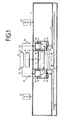
- the device shown in Figure 1 consists of a vacuum chamber 2, in which a substrate 3 is held and guided longitudinally displaceable, wherein above the substrate 3, a diaphragm 4 is provided with aperture 5, the precipitate of the atomized from the target 6 of the cathode 7 material the surface of the moving in the direction of arrow A substrate 3 is allowed.
- the cathode 7 is connected via a line 9 to a DC power source 8 and is otherwise separated by means of a cup-shaped housing 10 of the compartments 11 and 12, in each of which cathodes 13,14 are arranged, whose targets 15,16 respectively to the lower Wall portion 17 and 18 of the compartments 11,12 are aligned.
- the cathodes 13, 14 are each connected to a pole 20 or 21 of the alternating current source 19 via a respective current conductor 22, 23.
- gas supply lines 24,25 with nozzles 26,27 via the process gas into the gap 28, which is bounded by the target 6 on the one hand and the substrate 3 on the other hand, flows.
- the electrical conductors 22,23 are each connected via a resistor with diode 29,30 with the vacuum chamber 2 and the vacuum chamber 2 is also connected to vacuum pumps 31,32, and that in the plane of the target. 6 the diode cathode 7 gaps or openings 33 and 34 are provided, which connect the compartments 11,12 with the space 35 immediately in front of the target 6, so that the plasma generated by the magnetron cathodes 13,14 uniformly in front of the target Diode cathode (the cathode without magnet assembly) 7 in the room 35 burns. Further openings 35,36 in the outer walls of the compartments 11,12 allow the rapid evacuation of these compartments.
- the embodiment according to Figure 2 differs from that of Figure 1 in that the magnetron cathodes 13,14 are aligned so that their targets 15,16 the outer walls 37,38 of the compartments 11,12 are opposite.
- FIG. 3 differs from that of Figure 1 essentially in that the compartments 11,12 via rear openings or channels 39,40 in the walls 41,42, which face each other, communicate with each other.
- the TwinMag cathodes 13, 14 (arrangement of two magnetron cathodes) are equipped with a target 15, 16 made of carbon in order to obtain the lowest possible sputtering rate, because in this arrangement the sputtering effect of the magnetron discharge is undesirable.
- the diode cathode 7 is covered with a target 6, which contains the material to be sputtered. All three cathodes are in a vacuum chamber 2. The three cathodes each have a dark space shield. The dark space shields of the TwinMag cathodes are floating while the dark space shield of the diode cathode is grounded.
- the diode cathode 7 is connected to a DC power supply, wherein the positive pole of the power supply is connected to the vacuum chamber, that is grounded.
- the AC voltage (AC line voltage or center frequency or a frequency in between) is applied to the two TwinMag cathodes 13,14. Due to the alternating voltage, a plasma band develops between the two cathodes 13, 14. The spread of the plasma band is limited by the shielding of the device, so that the plasma band passes over the target of the diode cathode.
- the gas inlet is located below said shield so that the targets can not be struck directly by a gas jet.
Description
Die Erfindung betrifft eine Vorrichtung zum Beschichten eines Substrats von einem elektrisch leitfähigen Target, umfassend eine Wechselstromquelle, die mit zwei Magnetron-Kathoden verbunden ist, die elektrisch mit den Targets zusammenwirken, wobei der eine Pol der Wechselstromquelle an die eine Kathode und der andere Pol an die andere Kathode über Versorgungsleitungen angeschlossen ist.The invention relates to a device for coating a substrate of an electrically conductive target, comprising an AC power source which is connected to two magnetron cathodes, which cooperate electrically with the targets, wherein the one pole of the AC power source to the one cathode and the other pole the other cathode is connected via supply lines.
Bekannt ist eine Sputteranordnung, die als Triodenanordnung bezeichnet wird (low-voltage triode sputtering with a confined plasma; T. C. Tisone a. J. B. Bindell, J. of Vacuum Science a. Technology, Vol. 11, 1974, Seiten 519 bis 527), bei der das Plasma vor dem abzusputternden Target durch den Einsatz einer zusätzlichen Niedervolt-Gasentladung mit einer thermischen Kathode als Elektronenquelle verstärkt wird. Die Elektronen fließen in diesem Falle quer durch das Hauptentladungsplasma, wodurch die Ladungsträgerdichte erhöht und die Gasionisation verstärkt wird. Diese bekannte Vorrichtung hat jedoch den Nachteil, daß die mögliche Stromdichte begrenzt ist und insbesondere eine schlechte Langzeitstabilität aufweist.Known is a sputtering arrangement, referred to as triode assembly (Low-voltage triode sputtering with a confined plasma; TC Tisone, JB Bindell, J. of Vacuum Science a., Technology, Vol. 11, 1974, pages 519 to 527) the plasma in front of the sputtered target by the use of an additional low-voltage gas discharge with a thermal cathode as an electron source is reinforced. The electrons in this case flow across the main discharge plasma, thereby increasing the charge carrier density and increasing gas ionization. However, this known device has the disadvantage that the possible current density is limited and in particular has a poor long-term stability.
Es ist auch eine Zerstäubungseinrichtung zur Herstellung dünner Schichten bekannt (DD 252 205), bestehend aus einem Magnetsystem und mindestens zwei darüber angeordneten Elektroden aus dem zu zerstäubenden Material, wobei diese Elektroden elektrisch so gestaltet sind, daß sie wechselweise Kathode und Anode einer Gasentladung sind. Die Elektroden sind zu diesem Zwecke an eine sinusförmige Wechselspannung von vorzugweise 50 Hz angeschlossen.It is also a sputtering device for producing thin layers known (DD 252 205), consisting of a magnetic system and at least two electrodes arranged above it from the material to be sputtered, these electrodes are electrically designed so that they are alternately cathode and anode of a gas discharge. The electrodes are connected for this purpose to a sinusoidal AC voltage of preferably 50 Hz.
Diese bekannte Zerstäubungseinrichtung soll besonders für die Abscheidung dielektrischer Schichten durch reaktive Zerstäubung geeignet sein. Durch den Betrieb der Einrichtung mit etwa 50 Hz soll vermieden werden, daß es zur Flitterbildung an der Anode und im Falle von Metallbeschichtung zu elektrischen Kurzschlüssen (sogenannten Arcs) kommt.This known sputtering device should be particularly suitable for the deposition of dielectric layers by reactive sputtering. By operating the device at about 50 Hz to avoid that it comes to tinsel formation at the anode and in the case of metal coating to electrical short circuits (so-called arcs).
Bei einer anderen bereits bekannten Vorrichtung zum Aufstäuben eines dünnen Films, bei der die Geschwindigkeit des Niederbringens von Schichten unterschiedlicher Materialien regelbar ist (DE 39 12 572), um so zu extrem dünnen Schichtpaketen zu gelangen, sind mindestens zwei unterschiedliche Arten von kathodenseitig vorgesehenen Gegenelektroden angeordnet.In another already known device for sputtering a thin film, in which the speed of the deposition of layers of different materials is controllable (DE 39 12 572), so as to arrive at extremely thin layer packages are at least two different Types of counter-electrodes provided on the cathode side are arranged.
Weiterhin ist eine Anordnung zum Abscheiden einer Metalllegierung mit Hilfe von HF-Kathodenzerstäubung bekannt (DE 35 41 621), bei der abwechselnd zwei Targets angesteuert werden, wobei die Targets die Metallkomponenten der abzuscheidenden Metallegierung jedoch mit unterschiedlichen Anteilen enthalten. Die Substrate sind zu diesem Zweck auf einem Substratträger angeordnet, der von einer Antriebseinheit während des Zerstäubungsvorgangs in Rotation versetzt wird.Furthermore, an arrangement for depositing a metal alloy by means of RF cathode sputtering is known (
Durch eine vorveröffentlichte Druckschrift (DE 38 02 852) ist es außerdem bekannt, bei einer Einrichtung für die Beschichtung eines Substrats mit zwei Elektroden und wenigstens einem zu zerstäubenden Material das zu beschichtende Substrat zwischen den beiden Elektroden in einem räumlichen Abstand anzuordnen und die Wechselstrom-Halbwellen als niederfrequente Halbwellen mit im wesentlichen gleichen Amplituden zu wählen.By a previously published document (
Weiterhin sind ein Verfahren und eine Vorrichtung beschrieben (DE 41 06 770) zum reaktiven Beschichten eines Substrats mit einem elektrisch isolierenden Werkstoff, beispielsweise mit Siliziumdioxid (SiO2) bestehend aus einer Wechselstromquelle, die mit in einer Beschichtungskammer angeordneten Magnete einschließende Kathoden verbunden ist, die mit Targets zusammenwirken, wobei zwei erdfreie Ausgänge der Wechselstromquelle mit je einer ein Target tragenden Kathode verbunden sind, wobei beide Kathoden in der Beschichtungskammer nebeneinanderliegend in einem Plasmaraum vorgesehen sind und zum gegenüberliegenden Substrat jeweils etwa den gleichen räumlichen Abstand aufweisen. Der Effektivwert der Entladespannung wird dabei von einer über eine Leitung an die Kathode angeschlossenen Spannungseffektivwerterfassung gemessen und als Gleichspannung einem Regler über eine Leitung zugeführt, der über ein Regelventil den Reaktivgasfluß vom Behälter in die Verteilerleitung so steuert, daß die gemessene Spannung mit einer Sollspannung übereinstimmt.Furthermore, a method and a device are described (
Schließlich ist eine Vorrichtung zum Beschichten eines Substrats, insbesondere mit nichtleitenden Schichten von elektrisch leitfähigen Targets in reaktiver Atmosphäre bekannt (DE 42 04 999), bestehend aus einer Stromquelle, die mit in einer evakuierbaren Beschichtungskammer angeordneten, Magnete einschließenden Kathoden verbunden ist, die elektrisch mit den Targets zusammenwirken, wobei zwei elektrisch voneinander und von der Sputterkammer getrennte Anoden angeordnet sind, die in einer Ebene zwischen den Kathoden und dem Substrat vorgesehen sind, wobei die beiden Ausgänge der Sekundärwicklung eines mit einem Mittelfrequenzgenerator verbundenen Transformators jeweils an eine Kathode über Versorgungsleitungen angeschlossen sind, wobei die erste und die zweite Versorgungsleitung über eine Zweigleitung untereinander verbunden sind, in die ein Schwingkreis, vorzugsweise eine Spule und ein Kondensator, eingeschaltet sind, und wobei jede der beiden Versorgungsleitungen jeweils sowohl über ein das Gleichspannungspotential gegenüber Erde einstellendes erstes elektrisches Glied mit der Beschichtungskammer als auch über ein entsprechendes zweites elektrisches Glied mit der jeweiligen Anode und über jeweils eine Zweigleitung mit eingeschaltetem Kondensator mit der Beschichtungskammer verbunden ist und wobei eine Drosselspule in den den Schwingkreis mit dem zweiten Sekundäranschluß verbindenen Abschnitt der ersten Versorgungsleitung eingeschaltet ist.Finally, an apparatus for coating a substrate, in particular with non-conductive layers of electrically conductive targets in a reactive atmosphere is known (
Während die bekannten Vorrichtungen sich damit befassen, das "Arcing", d.h. die Bildung unerwünschter Lichtbögen zu verhindern und die Oberfläche der Targets vor der Bildung isolierender Schichten zu bewahren, soll der Gegenstand der vorliegenden Erfindung nicht nur die Langzeitstabilität und die Depositionsrate des Sputterprozesses erhöhen, sondern auch eine hohe Targetausnutzung und Gleichmäßigkeit gewährleisten.While the known devices are concerned with "arcing", i. To prevent the formation of unwanted arcing and to protect the surface of the targets from the formation of insulating layers, the object of the present invention is not only intended to increase the long-term stability and deposition rate of the sputtering process, but also to ensure high target utilization and uniformity.
Gemäß der vorliegenden Erfindung wird diese Aufgabe dadurch gelöst, daß jede der beiden Magnetron-Kathoden in einem eigenen Abteil innerhalb der Vakuumkammer angeordnet ist und beide Abteile über Spalte oder Öffnungen in ihren Trennwänden mit einem dritten Abteil verbunden sind, wobei im dritten Abteil eine Dioden-Kathode mit Sputtertarget vorgesehen ist, die über eine Leitung an eine eigene Gleichstrom-Versorgung angeschlossen ist, und wobei in den Raum zwischen Diodenkathode und dem dieser gegenüberliegenden Substrat Gasleitungen einmünden, über die das Prozeßgas in diesen Bereich zwischen dem Target der Dioden-Kathode und dem Substrat einlaßbar ist.According to the present invention, this object is achieved in that each of the two magnetron cathodes is arranged in a separate compartment within the vacuum chamber and both compartments are connected via gaps or openings in their partitions with a third compartment, wherein in the third compartment a diode Cathode is provided with a sputtering target, which is connected via a line to its own DC power supply, and wherein in the space between the diode cathode and the substrate opposite this gas lines open, via which the process gas in this area between the target of the diode cathode and the substrate is einlaßbar.
Weitere Einzelheiten und Merkmale sind in den Patentansprüchen näher erläutert und gekennzeichnet.Further details and features are explained in more detail in the claims and characterized.
Die Erfindung läßt die verschiedensten Ausführungsmöglichkeiten zu; drei davon sind in den anliegenden Zeichnungen schematisch dargestellt.The invention allows a variety of execution options; three of them are shown schematically in the accompanying drawings.
Die in Figur 1 dargestellte Vorrichtung besteht aus einer Vakuumkammer 2, in der ein Substrat 3 längsverschiebbar gehalten und geführt ist, wobei oberhalb des Substrats 3 eine Blende 4 mit Blendenöffnung 5 vorgesehen ist, die den Niederschlag des vom Target 6 der Kathode 7 abgestäubten Materials auf der Oberfläche des sich in Pfeilrichtung A bewegenden Substrats 3 gestattet. Die Kathode 7 ist über eine Leitung 9 an eine Gleichstromquelle 8 angeschlossen und ist im übrigen mit Hilfe eines topfförmigen Gehäuses 10 von den Abteilen 11 und 12 abgetrennt, in denen jeweils Kathoden 13,14 angeordnet sind, deren Targets 15,16 jeweils auf das untere Wandteil 17 bzw. 18 der Abteile 11,12 ausgerichtet sind. Die Kathoden 13,14 sind jeweils an einen Pol 20 bzw. 21 der Wechselstromquelle 19 über jeweils einen Stromleiter 22,23 angeschlossen. Unterhalb der Bodenteile 17,18 der Abteile 11,12 befinden sich Gaszufuhrleitungen 24,25 mit Düsen 26,27, über die Prozeßgas in den Zwischenraum 28, der von dem Target 6 einerseits und dem Substrat 3 andererseits begrenzt wird, einströmt.The device shown in Figure 1 consists of a
Es sei noch erwähnt, daß als Zündhilfe die elektrischen Stromleiter 22,23 jeweils über einen Widerstand mit Diode 29,30 mit der Vakuumkammer 2 verbunden sind und die Vakuumkammer 2 außerdem an Vakuumpumpen 31,32 angeschlossen ist, und daß in der Ebene des Targets 6 der Dioden-Kathode 7 Spalte oder Öffnungen 33 bzw. 34 vorgesehen sind, die die Abteile 11,12 mit dem Raum 35 unmittelbar vor dem Target 6 verbinden, so daß das von den Magnetron-Kathoden 13,14 erzeugte Plasma gleichmäßig vor dem Target der Dioden-Kathode (der Kathode ohne Magnetanordnung) 7 im Raum 35 brennt. Weitere Öffnungen 35,36 in den Außenwänden der Abteile 11,12 ermöglichen das rasche Evakuieren dieser Abteile.It should be noted that as a starting aid, the
Die Ausführungsform gemäß Figur 2 unterscheidet sich von derjenigen nach Figur 1 dadurch, daß die Magnetron-Kathoden 13,14 so ausgerichtet sind, daß ihre Targets 15,16 den Außenwänden 37,38 der Abteile 11,12 gegenüberliegen.The embodiment according to Figure 2 differs from that of Figure 1 in that the
Die Ausführungsform gemäß Figur 3 unterscheidet sich von derjenigen nach Figur 1 im Wesentlichen dadurch, daß die Abteile 11,12 über rückwärtige Öffnungen oder Kanäle 39,40 in den Wänden 41,42, die einander zugekehrt sind, miteinander in Verbindung stehen.The embodiment according to Figure 3 differs from that of Figure 1 essentially in that the
Ein Vorteil der erfindungsgemäßen Anordnung im Vergleich zu bekannten Anordnungen ist, daß mit Einsatz der auseinandergerückten Magnetron-Kathoden als zusätzliche Plasmaquelle (Elektronen und Ionen) die Plasmadichte direkt vor der genannten Dioden-Kathode wesentlich höher ist als in bekannten Anordnungen. Damit erreicht man:
- 1. höhere Depositionsrate,
- 2. gute Gleichmäßigkeit,
- 3. hohe Targetausnutzung,
- 4. hohe Langzeitstabilität,
- 5. großflächig statisches Sputtern mit guter Gleichmäßigkeit.
- 1. higher deposition rate,
- 2. good uniformity,
- 3. high target utilization,
- 4. high long-term stability,
- 5. large area static sputtering with good uniformity.
Die TwinMag-Kathoden 13,14 (Anordnung von zwei Magnetron-Kathoden) sind mit einem Target 15,16 aus Kohlenstoff bestückt, um eine möglichst geringe Sputterrate zu erhalten, weil bei dieser Anordnung der Sputtereffekt der Magnetronentladung unerwünscht ist. Die Dioden-Kathode 7 ist mit einem Target 6 belegt, das das zu sputternde Material enthält. Alle drei Kathoden befinden sich in einer Vakuumkammer 2. Die drei Kathoden haben jeweils eine Dunkelraumabschirmung. Die Dunkelraumabschirmungen der TwinMag-Kathoden sind floatend, während die Dunkelraumabschirmung der Dioden-Kathode geerdet ist. Die Dioden-Kathode 7 wird an eine Gleichspannungsstromversorgung angeschlossen, wobei der Pluspol der Stromversorgung mit der Vakuumkammer verbunden ist, d.h. geerdet ist. Die Wechselspannung (Netzwechselspannung oder Mittelfrequenz oder eine Frequenz dazwischen) wird an die beiden TwinMag-Kathoden 13,14 angelegt. Durch die Wechselspannung entwickelt sich ein Plasmaband zwischen beiden Kathoden 13,14. Die Ausbreitung des Plasmabandes wird durch die Abschirmung der Anordnung begrenzt, so daß das Plasmaband über das Target der Dioden-Kathode streicht. Der Gaseinlaß befindet sich unterhalb der genannten Abschirmung, so daß die Targets nicht direkt durch einen Gasstrahl getroffen werden können.The TwinMag
- 11
- Abteilcompartment
- 22
- Vakuumkammervacuum chamber
- 33
- Substratsubstratum
- 44
- Blendecover
- 55
- Blendenöffnungaperture
- 66
- Targettarget
- 77
- Kathodecathode
- 88th
- GleichstromquelleDC power source
- 99
- Leitung, StromleiterCable, conductor
- 1010
- topfförmiges Gehäusepot-shaped housing
- 1111
- Abteilcompartment
- 1212
- Abteilcompartment
- 1313
- Kathodecathode
- 1414
- Kathodecathode
- 1515
- Targettarget
- 1616
- Targettarget
- 1717
- Wandteilwall part
- 1818
- Wandteilwall part
- 1919
- WechselstromquelleAC power source
- 2020
- Pol, AnschlußPol, connection
- 2121
- Pol, AnschlußPol, connection
- 2222
- Stromleiterconductor
- 2323
- Stromleiterconductor
- 2424
- Gas-ZuleitungGas supply line
- 2525
- Gas-ZuleitungGas supply line
- 2626
- Düsejet
- 2727
- Düsejet
- 2828
- Zwischenraumgap
- 2929
- Widerstand mit DiodeResistor with diode
- 3030
- Widerstand mit DiodeResistor with diode
- 3131
- Vakuumpumpevacuum pump
- 3232
- Vakuumpumpevacuum pump
- 3333
- Spalt, Schlitz, ÖffnungGap, slot, opening
- 3434
- Spalt, Schlitz, ÖffnungGap, slot, opening
- 3535
- Öffnung, DurchbruchOpening, breakthrough
- 3636
- Öffnung, DurchbruchOpening, breakthrough
- 3737
- Außenwandouter wall
- 3838
- Außenwandouter wall
- 3939
- Kanalchannel
- 4040
- Kanalchannel
- 4141
- Wandteilwall part
- 4242
- Wandteilwall part
Claims (3)
- Apparatus for coating a substrate (3) from electrically conductive targets (15, 16), comprising an alternating current power source (19) connected with two magnetron cathodes (13, 14) that co-operate electrically with the targets (15, 16), the one pole (20) of the alternating current source (19) being connected to the one cathode (13) and the other pole (21) to the other cathode (14) via supply lines (22, 23), characterised in that each of the two magnetron cathodes (13, 14) is arranged in its own compartment (11, 12) within the vacuum chamber (2) and the two compartments (11, 12) are connected via gaps (33, 34) or openings in their partition walls with a third compartment (1) or with an area (25) immediately in front of this third compartment (1), where in the third compartment (1) is arranged a diode cathode (7) with sputter target (6) that is connected via a line (9) to its own direct current source (8), and where in the space (28) between the diode cathode (7) and the substrate plane (3) arranged opposite this open gas lines (24, 25) via which the process gas can be introduced into this area (28) between the target (6) of the diode cathode (7) and the substrate (3).
- Apparatus according to claim 1, further characterised in that the magnetron cathodes (13, 14) are aligned such that the plane of their targets (15, 16) extends parallel to the floor parts (17, 18) opposite the substrate plane or that the planes of their targets (15, 16) are parallel to the side walls (37, 48) limiting the compartments (11, 12) to the outside.
- Apparatus according to claims 1 and 2, further characterised in that the two compartments (11, 12) containing the magnetron cathodes (13, 14) are surrounded by the vacuum chamber (2) and the floor parts (17, 18) of the compartments (11, 12) extend in a plane which runs parallel to the plane of the targets (6) of the diode cathode (7) and parallel to the substrate plane (3) and the two slots or openings (33, 34) for outlet of the plasma current are diametrically opposed in the mutually facing side walls (41, 42) of the compartments and in a plane below the plane of the target (6) of the diode cathode (7).
Applications Claiming Priority (2)
| Application Number | Priority Date | Filing Date | Title |
|---|---|---|---|
| DE19540794 | 1995-11-02 | ||
| DE19540794A DE19540794A1 (en) | 1995-11-02 | 1995-11-02 | Device for coating a substrate from an electrically conductive target |
Publications (3)
| Publication Number | Publication Date |
|---|---|
| EP0772223A2 EP0772223A2 (en) | 1997-05-07 |
| EP0772223A3 EP0772223A3 (en) | 2004-11-10 |
| EP0772223B1 true EP0772223B1 (en) | 2007-01-03 |
Family
ID=7776415
Family Applications (1)
| Application Number | Title | Priority Date | Filing Date |
|---|---|---|---|
| EP96111817A Expired - Lifetime EP0772223B1 (en) | 1995-11-02 | 1996-07-23 | Device for coating a substrate from electrically conductive targets |
Country Status (6)
| Country | Link |
|---|---|
| US (1) | US5718815A (en) |
| EP (1) | EP0772223B1 (en) |
| JP (1) | JP3995062B2 (en) |
| KR (1) | KR100210268B1 (en) |
| DE (2) | DE19540794A1 (en) |
| TW (1) | TW328608B (en) |
Families Citing this family (19)
| Publication number | Priority date | Publication date | Assignee | Title |
|---|---|---|---|---|
| DE19506515C1 (en) * | 1995-02-24 | 1996-03-07 | Fraunhofer Ges Forschung | Reactive coating process using a magnetron vaporisation source |
| DE59611403D1 (en) * | 1995-10-27 | 2007-01-25 | Applied Materials Gmbh & Co Kg | Device for coating a substrate |
| DE19644752A1 (en) * | 1996-10-28 | 1998-04-30 | Leybold Systems Gmbh | Interference layer system |
| DE19651378A1 (en) * | 1996-12-11 | 1998-06-18 | Leybold Systems Gmbh | Insulating thin film sputter deposition apparatus |
| DE19733940C2 (en) * | 1997-08-06 | 2001-03-01 | Leybold Systems Gmbh | Device for coating plate-shaped substrates with thin layers by means of cathode sputtering |
| DE19741708A1 (en) * | 1997-09-22 | 1999-04-01 | Leybold Systems Gmbh | Apparatus for coating a substrate with thin layers |
| DE29717418U1 (en) * | 1997-09-26 | 1998-01-22 | Leybold Systems Gmbh | Device for applying thin layers on a substrate |
| DE19813075A1 (en) * | 1998-03-25 | 1999-09-30 | Leybold Ag | Device for coating a substrate |
| US6620298B1 (en) * | 1999-04-23 | 2003-09-16 | Matsushita Electric Industrial Co., Ltd. | Magnetron sputtering method and apparatus |
| US7411352B2 (en) * | 2002-09-19 | 2008-08-12 | Applied Process Technologies, Inc. | Dual plasma beam sources and method |
| DE10362259B4 (en) * | 2003-11-04 | 2011-03-17 | Von Ardenne Anlagentechnik Gmbh | Long-stretched vacuum system for one or two-sided coating of flat substrates |
| KR200377696Y1 (en) * | 2004-12-03 | 2005-03-11 | 동 호 김 | a flash remocon |
| JP2012518894A (en) * | 2009-02-02 | 2012-08-16 | リンデール インコーポレイテッド | Method of manufacturing a mechanical device having a high density capacitor or other microscopic layer |
| JP6092721B2 (en) * | 2013-06-21 | 2017-03-08 | 株式会社アルバック | Deposition equipment |
| CN114373669A (en) | 2017-06-27 | 2022-04-19 | 佳能安内华股份有限公司 | Plasma processing apparatus |
| KR102257134B1 (en) | 2017-06-27 | 2021-05-26 | 캐논 아네르바 가부시키가이샤 | Plasma treatment device |
| PL3648550T3 (en) | 2017-06-27 | 2021-11-22 | Canon Anelva Corporation | Plasma treatment device |
| SG11201912564VA (en) | 2017-06-27 | 2020-01-30 | Canon Anelva Corp | Plasma processing apparatus |
| WO2020003557A1 (en) * | 2018-06-26 | 2020-01-02 | キヤノンアネルバ株式会社 | Plasma treatment device, plasma treatment method, program, and memory medium |
Family Cites Families (14)
| Publication number | Priority date | Publication date | Assignee | Title |
|---|---|---|---|---|
| DE252205C (en) | ||||
| US4629548A (en) * | 1985-04-03 | 1986-12-16 | Varian Associates, Inc. | Planar penning magnetron sputtering device |
| DE3541621A1 (en) * | 1985-11-25 | 1987-05-27 | Siemens Ag | Arrangement for depositing a metal alloy |
| JPH01158644A (en) * | 1987-12-14 | 1989-06-21 | Matsushita Electric Ind Co Ltd | Producing device for magneto-optical recording carrier |
| DE3802852A1 (en) * | 1988-02-01 | 1989-08-03 | Leybold Ag | Device for coating a substrate with a material obtained from a plasma |
| US4911814A (en) * | 1988-02-08 | 1990-03-27 | Nippon Telegraph And Telephone Corporation | Thin film forming apparatus and ion source utilizing sputtering with microwave plasma |
| JPH01268869A (en) | 1988-04-20 | 1989-10-26 | Fuji Photo Film Co Ltd | Sputtering device |
| JPH0826453B2 (en) * | 1988-12-26 | 1996-03-13 | 富士写真フイルム株式会社 | Sputtering equipment |
| DE4106770C2 (en) * | 1991-03-04 | 1996-10-17 | Leybold Ag | Performing reactive coating of a substrate |
| DE4120690A1 (en) * | 1991-06-22 | 1992-12-24 | Leybold Ag | Ferromagnetic target for magnetron electrode - has first part between north and south poles of permanent magnet and second part opposite poles |
| US5415757A (en) * | 1991-11-26 | 1995-05-16 | Leybold Aktiengesellschaft | Apparatus for coating a substrate with electrically nonconductive coatings |
| DE4204999A1 (en) * | 1991-11-26 | 1993-08-26 | Leybold Ag | METHOD AND DEVICE FOR COATING A SUBSTRATE, ESPECIALLY WITH ELECTRICALLY NON-CONDUCTING LAYERS |
| DE4237517A1 (en) * | 1992-11-06 | 1994-05-11 | Leybold Ag | Reactive magnetron sputtering appts. - esp. for coating substrate with electrically non-conductibe layers |
| DE4326100B4 (en) * | 1993-08-04 | 2006-03-23 | Unaxis Deutschland Holding Gmbh | Method and apparatus for coating substrates in a vacuum chamber, with means for detecting and suppressing unwanted arcing |
-
1995
- 1995-11-02 DE DE19540794A patent/DE19540794A1/en not_active Withdrawn
-
1996
- 1996-07-23 DE DE59611407T patent/DE59611407D1/en not_active Expired - Lifetime
- 1996-07-23 EP EP96111817A patent/EP0772223B1/en not_active Expired - Lifetime
- 1996-08-10 TW TW085109722A patent/TW328608B/en not_active IP Right Cessation
- 1996-09-12 US US08/711,885 patent/US5718815A/en not_active Expired - Lifetime
- 1996-10-23 KR KR1019960047632A patent/KR100210268B1/en not_active IP Right Cessation
- 1996-11-01 JP JP29167796A patent/JP3995062B2/en not_active Expired - Lifetime
Also Published As
| Publication number | Publication date |
|---|---|
| JP3995062B2 (en) | 2007-10-24 |
| TW328608B (en) | 1998-03-21 |
| EP0772223A2 (en) | 1997-05-07 |
| DE19540794A1 (en) | 1997-05-07 |
| KR100210268B1 (en) | 1999-07-15 |
| KR970030004A (en) | 1997-06-26 |
| JPH09170078A (en) | 1997-06-30 |
| DE59611407D1 (en) | 2007-02-15 |
| US5718815A (en) | 1998-02-17 |
| EP0772223A3 (en) | 2004-11-10 |
Similar Documents
| Publication | Publication Date | Title |
|---|---|---|
| EP0772223B1 (en) | Device for coating a substrate from electrically conductive targets | |
| EP0782173B1 (en) | Apparatus for coating a substrate by means of a chemical vapour deposition process | |
| DE19651811B4 (en) | Device for covering a substrate with thin layers | |
| EP0593924B1 (en) | Device for producing plasma using cathodic sputtering | |
| DE3920835C2 (en) | Device for coating substrates | |
| EP0783174B1 (en) | Apparatus for coating a substrate | |
| EP0502242B1 (en) | Reactive sputtering apparatus | |
| EP3309815B1 (en) | Plasma treatment device with two microwave plasma sources coupled together and method for operating such a plasma treatment device | |
| EP0958195B1 (en) | Method for coating surfaces using an installation with sputter electrodes | |
| DE3521053A1 (en) | DEVICE FOR APPLYING THIN LAYERS TO A SUBSTRATE | |
| DE2608415A1 (en) | METHOD OF COATING A SUBSTRATE WITH A LAYER OF POLYMERIC MATERIAL | |
| DE19651378A1 (en) | Insulating thin film sputter deposition apparatus | |
| EP0755461A1 (en) | Process and device for ion-supported vacuum coating | |
| DE3802852C2 (en) | ||
| DE19939040B4 (en) | Magnetronsputtergerät | |
| EP2585622A1 (en) | Arc deposition source having a defined electric field | |
| DE4336830A1 (en) | Plasma sputtering installation with microwave assistance | |
| WO2000039355A1 (en) | Method and device for coating substrates by means of bipolar pulse magnetron sputtering and the use thereof | |
| EP0775758A1 (en) | Vacuum coating apparatus with a crucible located in the vacuum chamber to receive the evaporation material | |
| DE3226717C2 (en) | ||
| EP0544107B1 (en) | Method and apparatus for coating a substrate, in particular for electrical insulating layers | |
| DE4230291A1 (en) | Microwave-assisted sputtering appts. - comprises vacuum chamber, target, magnetic appts., microwave, and electromagnet | |
| EP0811238B1 (en) | Reactive sputtering device | |
| EP0776987B1 (en) | Vacuum coating apparatus with a crucible located in the vacuum chamber to receive the evaporation material | |
| DE4138793C2 (en) | Method and device for coating a substrate, in particular with electrically non-conductive layers |
Legal Events
| Date | Code | Title | Description |
|---|---|---|---|
| PUAI | Public reference made under article 153(3) epc to a published international application that has entered the european phase |
Free format text: ORIGINAL CODE: 0009012 |
|
| AK | Designated contracting states |
Kind code of ref document: A2 Designated state(s): BE CH DE ES FR GB IT LI LU NL SE |
|
| PUAL | Search report despatched |
Free format text: ORIGINAL CODE: 0009013 |
|
| AK | Designated contracting states |
Kind code of ref document: A3 Designated state(s): BE CH DE ES FR GB IT LI LU NL SE |
|
| RAP1 | Party data changed (applicant data changed or rights of an application transferred) |
Owner name: UNAXIS DEUTSCHLAND HOLDING GMBH |
|
| 17P | Request for examination filed |
Effective date: 20050504 |
|
| GRAP | Despatch of communication of intention to grant a patent |
Free format text: ORIGINAL CODE: EPIDOSNIGR1 |
|
| RTI1 | Title (correction) |
Free format text: DEVICE FOR COATING A SUBSTRATE FROM ELECTRICALLY CONDUCTIVE TARGETS |
|
| GRAS | Grant fee paid |
Free format text: ORIGINAL CODE: EPIDOSNIGR3 |
|
| RAP1 | Party data changed (applicant data changed or rights of an application transferred) |
Owner name: UNAXIS DEUTSCHLAND HOLDING GMBH |
|
| RAP1 | Party data changed (applicant data changed or rights of an application transferred) |
Owner name: OERLIKON DEUTSCHLAND HOLDING GMBH |
|
| GRAA | (expected) grant |
Free format text: ORIGINAL CODE: 0009210 |
|
| AK | Designated contracting states |
Kind code of ref document: B1 Designated state(s): BE CH DE ES FR GB IT LI LU NL SE |
|
| REG | Reference to a national code |
Ref country code: GB Ref legal event code: FG4D Free format text: NOT ENGLISH |
|
| GBT | Gb: translation of ep patent filed (gb section 77(6)(a)/1977) |
Effective date: 20070105 |
|
| REF | Corresponds to: |
Ref document number: 59611407 Country of ref document: DE Date of ref document: 20070215 Kind code of ref document: P |
|
| PG25 | Lapsed in a contracting state [announced via postgrant information from national office to epo] |
Ref country code: SE Free format text: LAPSE BECAUSE OF FAILURE TO SUBMIT A TRANSLATION OF THE DESCRIPTION OR TO PAY THE FEE WITHIN THE PRESCRIBED TIME-LIMIT Effective date: 20070403 |
|
| PG25 | Lapsed in a contracting state [announced via postgrant information from national office to epo] |
Ref country code: ES Free format text: LAPSE BECAUSE OF FAILURE TO SUBMIT A TRANSLATION OF THE DESCRIPTION OR TO PAY THE FEE WITHIN THE PRESCRIBED TIME-LIMIT Effective date: 20070414 |
|
| ET | Fr: translation filed | ||
| PLBE | No opposition filed within time limit |
Free format text: ORIGINAL CODE: 0009261 |
|
| STAA | Information on the status of an ep patent application or granted ep patent |
Free format text: STATUS: NO OPPOSITION FILED WITHIN TIME LIMIT |
|
| 26N | No opposition filed |
Effective date: 20071005 |
|
| BERE | Be: lapsed |
Owner name: OERLIKON DEUTSCHLAND HOLDING G.M.B.H. Effective date: 20070731 |
|
| PG25 | Lapsed in a contracting state [announced via postgrant information from national office to epo] |
Ref country code: BE Free format text: LAPSE BECAUSE OF NON-PAYMENT OF DUE FEES Effective date: 20070731 |
|
| PG25 | Lapsed in a contracting state [announced via postgrant information from national office to epo] |
Ref country code: LU Free format text: LAPSE BECAUSE OF NON-PAYMENT OF DUE FEES Effective date: 20070723 |
|
| REG | Reference to a national code |
Ref country code: FR Ref legal event code: PLFP Year of fee payment: 20 |
|
| PGFP | Annual fee paid to national office [announced via postgrant information from national office to epo] |
Ref country code: FR Payment date: 20150626 Year of fee payment: 20 |
|
| PGFP | Annual fee paid to national office [announced via postgrant information from national office to epo] |
Ref country code: NL Payment date: 20150721 Year of fee payment: 20 |
|
| PGFP | Annual fee paid to national office [announced via postgrant information from national office to epo] |
Ref country code: CH Payment date: 20150721 Year of fee payment: 20 Ref country code: DE Payment date: 20150721 Year of fee payment: 20 Ref country code: GB Payment date: 20150721 Year of fee payment: 20 |
|
| PGFP | Annual fee paid to national office [announced via postgrant information from national office to epo] |
Ref country code: IT Payment date: 20150729 Year of fee payment: 20 |
|
| REG | Reference to a national code |
Ref country code: DE Ref legal event code: R071 Ref document number: 59611407 Country of ref document: DE |
|
| REG | Reference to a national code |
Ref country code: NL Ref legal event code: MK Effective date: 20160722 |
|
| REG | Reference to a national code |
Ref country code: CH Ref legal event code: PL |
|
| REG | Reference to a national code |
Ref country code: GB Ref legal event code: PE20 Expiry date: 20160722 |
|
| PG25 | Lapsed in a contracting state [announced via postgrant information from national office to epo] |
Ref country code: GB Free format text: LAPSE BECAUSE OF EXPIRATION OF PROTECTION Effective date: 20160722 |