JP4904165B2 - Method and apparatus for monitoring optical properties of thin films during a deposition process - Google Patents
Method and apparatus for monitoring optical properties of thin films during a deposition process Download PDFInfo
- Publication number
- JP4904165B2 JP4904165B2 JP2006549694A JP2006549694A JP4904165B2 JP 4904165 B2 JP4904165 B2 JP 4904165B2 JP 2006549694 A JP2006549694 A JP 2006549694A JP 2006549694 A JP2006549694 A JP 2006549694A JP 4904165 B2 JP4904165 B2 JP 4904165B2
- Authority
- JP
- Japan
- Prior art keywords
- substrate
- coating
- electromagnetic wave
- wave beam
- monitoring
- Prior art date
- Legal status (The legal status is an assumption and is not a legal conclusion. Google has not performed a legal analysis and makes no representation as to the accuracy of the status listed.)
- Expired - Fee Related
Links
- 230000003287 optical effect Effects 0.000 title claims description 78
- 238000012544 monitoring process Methods 0.000 title claims description 65
- 238000000034 method Methods 0.000 title claims description 62
- 239000010409 thin film Substances 0.000 title description 14
- 238000005137 deposition process Methods 0.000 title description 13
- 239000000758 substrate Substances 0.000 claims description 191
- 238000000576 coating method Methods 0.000 claims description 81
- 239000011248 coating agent Substances 0.000 claims description 76
- 238000000151 deposition Methods 0.000 claims description 55
- 230000008021 deposition Effects 0.000 claims description 44
- 239000000463 material Substances 0.000 claims description 34
- 238000004544 sputter deposition Methods 0.000 claims description 18
- 238000002834 transmittance Methods 0.000 claims description 5
- 230000032258 transport Effects 0.000 claims description 5
- 230000008859 change Effects 0.000 claims description 3
- 239000010410 layer Substances 0.000 description 54
- 230000008569 process Effects 0.000 description 29
- 230000005540 biological transmission Effects 0.000 description 11
- 238000004886 process control Methods 0.000 description 9
- 238000009501 film coating Methods 0.000 description 8
- 238000006243 chemical reaction Methods 0.000 description 7
- 238000012937 correction Methods 0.000 description 7
- 239000010408 film Substances 0.000 description 6
- 238000010521 absorption reaction Methods 0.000 description 5
- 230000008901 benefit Effects 0.000 description 4
- 238000010586 diagram Methods 0.000 description 4
- 238000004519 manufacturing process Methods 0.000 description 4
- 230000008020 evaporation Effects 0.000 description 3
- 238000001704 evaporation Methods 0.000 description 3
- 239000002356 single layer Substances 0.000 description 3
- VYPSYNLAJGMNEJ-UHFFFAOYSA-N Silicium dioxide Chemical compound O=[Si]=O VYPSYNLAJGMNEJ-UHFFFAOYSA-N 0.000 description 2
- 230000004907 flux Effects 0.000 description 2
- 238000005259 measurement Methods 0.000 description 2
- 239000012788 optical film Substances 0.000 description 2
- 238000005546 reactive sputtering Methods 0.000 description 2
- 238000000427 thin-film deposition Methods 0.000 description 2
- 230000004913 activation Effects 0.000 description 1
- 238000013459 approach Methods 0.000 description 1
- 238000010923 batch production Methods 0.000 description 1
- 230000015572 biosynthetic process Effects 0.000 description 1
- 238000004891 communication Methods 0.000 description 1
- 230000003750 conditioning effect Effects 0.000 description 1
- 239000000835 fiber Substances 0.000 description 1
- 238000001914 filtration Methods 0.000 description 1
- 238000012986 modification Methods 0.000 description 1
- 230000004048 modification Effects 0.000 description 1
- 230000035699 permeability Effects 0.000 description 1
- 230000004044 response Effects 0.000 description 1
- 238000012552 review Methods 0.000 description 1
- 239000000377 silicon dioxide Substances 0.000 description 1
- 229910052715 tantalum Inorganic materials 0.000 description 1
- GUVRBAGPIYLISA-UHFFFAOYSA-N tantalum atom Chemical compound [Ta] GUVRBAGPIYLISA-UHFFFAOYSA-N 0.000 description 1
Images


Classifications
-
- H—ELECTRICITY
- H01—ELECTRIC ELEMENTS
- H01J—ELECTRIC DISCHARGE TUBES OR DISCHARGE LAMPS
- H01J37/00—Discharge tubes with provision for introducing objects or material to be exposed to the discharge, e.g. for the purpose of examination or processing thereof
- H01J37/32—Gas-filled discharge tubes
- H01J37/32917—Plasma diagnostics
- H01J37/32935—Monitoring and controlling tubes by information coming from the object and/or discharge
-
- C—CHEMISTRY; METALLURGY
- C23—COATING METALLIC MATERIAL; COATING MATERIAL WITH METALLIC MATERIAL; CHEMICAL SURFACE TREATMENT; DIFFUSION TREATMENT OF METALLIC MATERIAL; COATING BY VACUUM EVAPORATION, BY SPUTTERING, BY ION IMPLANTATION OR BY CHEMICAL VAPOUR DEPOSITION, IN GENERAL; INHIBITING CORROSION OF METALLIC MATERIAL OR INCRUSTATION IN GENERAL
- C23C—COATING METALLIC MATERIAL; COATING MATERIAL WITH METALLIC MATERIAL; SURFACE TREATMENT OF METALLIC MATERIAL BY DIFFUSION INTO THE SURFACE, BY CHEMICAL CONVERSION OR SUBSTITUTION; COATING BY VACUUM EVAPORATION, BY SPUTTERING, BY ION IMPLANTATION OR BY CHEMICAL VAPOUR DEPOSITION, IN GENERAL
- C23C14/00—Coating by vacuum evaporation, by sputtering or by ion implantation of the coating forming material
- C23C14/22—Coating by vacuum evaporation, by sputtering or by ion implantation of the coating forming material characterised by the process of coating
- C23C14/54—Controlling or regulating the coating process
- C23C14/542—Controlling the film thickness or evaporation rate
- C23C14/545—Controlling the film thickness or evaporation rate using measurement on deposited material
- C23C14/547—Controlling the film thickness or evaporation rate using measurement on deposited material using optical methods
-
- G—PHYSICS
- G01—MEASURING; TESTING
- G01B—MEASURING LENGTH, THICKNESS OR SIMILAR LINEAR DIMENSIONS; MEASURING ANGLES; MEASURING AREAS; MEASURING IRREGULARITIES OF SURFACES OR CONTOURS
- G01B11/00—Measuring arrangements characterised by the use of optical techniques
- G01B11/02—Measuring arrangements characterised by the use of optical techniques for measuring length, width or thickness
- G01B11/06—Measuring arrangements characterised by the use of optical techniques for measuring length, width or thickness for measuring thickness ; e.g. of sheet material
- G01B11/0616—Measuring arrangements characterised by the use of optical techniques for measuring length, width or thickness for measuring thickness ; e.g. of sheet material of coating
- G01B11/0625—Measuring arrangements characterised by the use of optical techniques for measuring length, width or thickness for measuring thickness ; e.g. of sheet material of coating with measurement of absorption or reflection
-
- G—PHYSICS
- G01—MEASURING; TESTING
- G01B—MEASURING LENGTH, THICKNESS OR SIMILAR LINEAR DIMENSIONS; MEASURING ANGLES; MEASURING AREAS; MEASURING IRREGULARITIES OF SURFACES OR CONTOURS
- G01B11/00—Measuring arrangements characterised by the use of optical techniques
- G01B11/02—Measuring arrangements characterised by the use of optical techniques for measuring length, width or thickness
- G01B11/06—Measuring arrangements characterised by the use of optical techniques for measuring length, width or thickness for measuring thickness ; e.g. of sheet material
- G01B11/0616—Measuring arrangements characterised by the use of optical techniques for measuring length, width or thickness for measuring thickness ; e.g. of sheet material of coating
- G01B11/0683—Measuring arrangements characterised by the use of optical techniques for measuring length, width or thickness for measuring thickness ; e.g. of sheet material of coating measurement during deposition or removal of the layer
Description
(関連出願)
本出願は、2004年1月15日出願の米国特許仮出願第60/536,500号の優先権を主張するものであり、その全体を参照により本明細書に組み込まれている。
(Related application)
This application claims priority from US Provisional Application No. 60 / 536,500, filed Jan. 15, 2004, which is incorporated herein by reference in its entirety.
本発明は、全体的に薄膜被覆に関する。さらに詳細には、本発明は、堆積工程中に薄膜被覆の選択された特性を監視し、それに応答して堆積工程を制御する方法および装置に関する。 The present invention relates generally to thin film coatings. More particularly, the present invention relates to a method and apparatus for monitoring selected properties of a thin film coating during a deposition process and controlling the deposition process in response thereto.
薄膜、特に多層膜を含む光学フィルターは多くの商業的な用途を有する。例えば、精密光学フィルターは、高密度波長分割多重送信(「DWDM」)におけるファイバー光通信産業に広い用途が見出された。多層薄膜被覆は、多層被覆を形成する個別の層の厚さを正確に制御することによって向上できることはよく知られている。 Optical filters including thin films, particularly multilayer films, have many commercial applications. For example, precision optical filters have found wide application in the fiber optic communications industry in Dense Wavelength Division Multiplexing (“DWDM”). It is well known that multilayer thin film coatings can be improved by precisely controlling the thickness of the individual layers that form the multilayer coating.
DWDMフィルターの実施例において、フィルターは、対応する波長帯域内の実質上全ての光を透過し、チャンネル外側の実質上全ての光を反射するように形成される。対応する波長帯内の実質上全ての光を透過し、帯域外側の実質上全ての光を反射する望ましい特性を満足する光学フィルターは、厚い空洞層を挿入した一連の四分の一波スタック(「QWS」)から形成できることは周知である。QWSフィルターは異なる屈折率を有する材料の交互層を堆積することによって形成することができる。典型的に、シリカなどの1種の材料(L)は比較的低い屈折率を有し、四酸化タンタルなどの他の材料(H)は比較的高い屈折率を有する。QWSはH材料を堆積し、次いでL材料の層、次いでH材料の層等、フィルターが望ましい光学特性に達するまで堆積することによって形成される。 In the embodiment of the DWDM filter, the filter is configured to transmit substantially all light within the corresponding wavelength band and reflect substantially all light outside the channel. An optical filter that satisfies the desirable property of transmitting substantially all light in the corresponding wavelength band and reflecting substantially all light outside the band is a series of quarter wave stacks with a thick cavity layer inserted ( It is well known that it can be formed from “QWS”). QWS filters can be formed by depositing alternating layers of materials having different refractive indices. Typically, one material (L) such as silica has a relatively low refractive index and another material (H) such as tantalum tetroxide has a relatively high refractive index. QWS is formed by depositing H material and then depositing a layer of L material, then a layer of H material, etc., until the filter reaches the desired optical properties.
多層薄膜被覆を形成するとき、被覆の光学的性能は個々の層の厚さを正確に制御することによって大きく改善することができる。交互層の望ましい厚さを数学的に計算することが可能であり、したがって、各層の「中断(cut−off)」点を各材料の既知の堆積速度から求めることができる。しかし、薄膜堆積の既知の方法は、完全に数学的計算に依存して堆積工程を制御するほど十分正確ではない。有用な被覆を得るために堆積工程の不正確さを克服するひとつの既知の方法は、堆積された被覆の光学的特性の関数として堆積工程を制御することである。 When forming a multilayer thin film coating, the optical performance of the coating can be greatly improved by precisely controlling the thickness of the individual layers. The desired thickness of the alternating layers can be calculated mathematically, so that the “cut-off” point of each layer can be determined from the known deposition rate of each material. However, known methods of thin film deposition are not accurate enough to control the deposition process completely relying on mathematical calculations. One known method of overcoming inaccuracies in the deposition process to obtain a useful coating is to control the deposition process as a function of the optical properties of the deposited coating.
例えば、正確な光学フィルターを作るひとつの既知の方法は、イオン銃を援用したe−ビーム蒸着工程で薄膜被覆を形成することによる。図1を参照すれば、堆積室10はH材料およびL材料の点源12、14と、塗工すべき基板16を収容する。典型的に、基板16は直径約3インチの円であり、基板表面の被覆の均一性を改善するために約1000rpmで回転させることができる。材料は、材料源の起動を交互に行うことによって交互層に堆積することができる。各層の厚さは、光源20から対象波長(λc)の光18のビームを導き、検出器22で光ビーム18の強度を測定することによって、塗工された基板16の波長λcでの透過率を監視することによって制御することができる。堆積している材料の厚さが「中断」点に達したことを監視器が示すとき、各材料の堆積を「中断」することができる。典型的にe−ビーム蒸着工程における堆積工程は各層あたり約5分間かかる。
For example, one known method of making an accurate optical filter is by forming a thin film coating in an e-beam evaporation process with the aid of an ion gun. Referring to FIG. 1, a deposition chamber 10 contains H and L
しかし、図示したように、それらの光学的監視システムは基板の光源に対する位置が固定されているシステム(基板をその軸の周りに回転させることができるが)において見出される。アレーを形成する多数の基板が堆積すべき材料源を過ぎて移動する「バッチ」工程において、薄膜被覆を形成することがしばしば望まれる。それらのバッチ工程において、静止状態の参考基板を光学的に監視することが知られている。しかし、堆積室内の塗工フラックスの空間的変動のため、塗工している基板のアレーはアレー中の他の基板および参考基板とは異なる塗工フラックスに露出され、従ってアレー中の異なる基板には異なる速度で被覆が形成される。これは基板のアレー中の被覆の変動を招く。基板アレー内の被覆の均一性は基板を室全体に動かすことによって改善することができるが、参考基板は静止状態に留まる。塗工材料源を過ぎて移動する基板を光学的に監視し、アレー中の複数の基板を光学的に監視する方法および装置が必要である。さらに、基板がビーム源を過ぎて移動する際に監視ビームの入射角が変化する場合、基板を光学的に監視する必要がある。 However, as shown, these optical monitoring systems are found in systems where the position of the substrate relative to the light source is fixed (although the substrate can be rotated about its axis). It is often desirable to form a thin film coating in a “batch” process in which a large number of substrates forming the array move past the source of material to be deposited. It is known to optically monitor a stationary reference substrate during these batch processes. However, due to the spatial variation of the coating flux within the deposition chamber, the array of substrates being coated is exposed to a different coating flux than the other substrates in the array and the reference substrate, and therefore on different substrates in the array. The coatings are formed at different rates. This leads to coating variations in the array of substrates. The uniformity of the coating within the substrate array can be improved by moving the substrate throughout the chamber, but the reference substrate remains stationary. What is needed is a method and apparatus for optically monitoring a substrate moving past a source of coating material and optically monitoring a plurality of substrates in the array. Furthermore, if the angle of incidence of the monitoring beam changes as the substrate moves past the beam source, the substrate must be optically monitored.
したがって、本発明の目的は、従来技術の上記欠点の多くを回避し、堆積工程中に基板上に形成された被覆の選択された光学特性を監視する新規な方法および装置を提供することである。
本発明の他の目的は、塗工材料源を過ぎて移動する基板上に形成された被覆の選択された光学特性を監視する新規な方法および装置を提供することである。
本発明のさらに他の目的は、アレー中の複数の基板上に形成された被覆の選択された光学特性を監視する新規な方法および装置を提供することである。
本発明のさらに他の目的は、基板がビーム源を過ぎて移動する際に監視ビームの入射角度が変化する場合、基板上に形成された被覆の選択された光学特性を監視する新規な方法および装置を提供することである。
本発明のさらに他の目的は、スパッタ堆積工程で基板上に形成された被覆の選択された光学特性を監視する新規な方法および装置を提供することである。
本発明のさらに他の目的は、基板が回転ドラムで搬送されるスパッタ堆積工程で基板上に形成された被覆の選択された光学特性を監視する新規な方法および装置を提供することである。
本発明のさらに他の目的は、基板上に形成された被覆の選択された光学特性を監視するシステムにおいて、信号対ノイズ比を改善する新規な方法および装置を提供することである。
本発明のさらに他の目的は、基板上に形成された被覆の選択された光学特性を監視するシステムにおいて、構成要素を配列する新規な方法および装置を提供することである。
Accordingly, it is an object of the present invention to provide a novel method and apparatus that avoids many of the above disadvantages of the prior art and monitors selected optical properties of a coating formed on a substrate during the deposition process. .
Another object of the present invention is to provide a novel method and apparatus for monitoring selected optical properties of a coating formed on a substrate moving past a coating material source.
Yet another object of the present invention is to provide a novel method and apparatus for monitoring selected optical properties of coatings formed on a plurality of substrates in an array.
Yet another object of the present invention is to provide a novel method and method for monitoring selected optical properties of a coating formed on a substrate when the angle of incidence of the monitoring beam changes as the substrate moves past the beam source. Is to provide a device.
Yet another object of the present invention is to provide a novel method and apparatus for monitoring selected optical properties of a coating formed on a substrate in a sputter deposition process.
Yet another object of the present invention is to provide a novel method and apparatus for monitoring selected optical properties of a coating formed on a substrate in a sputter deposition process in which the substrate is conveyed on a rotating drum.
Yet another object of the present invention is to provide a novel method and apparatus for improving the signal-to-noise ratio in a system for monitoring selected optical properties of a coating formed on a substrate.
Yet another object of the present invention is to provide a novel method and apparatus for arranging components in a system for monitoring selected optical properties of a coating formed on a substrate.
本発明のこれらの目的、および多くの他の目的および利点は、当業者であれば、請求項、添付図面、および以下の好ましい実施形態の詳細な説明を熟読することによって、容易に明らかになるであろう。 These and many other objects and advantages of the present invention will be readily apparent to one of ordinary skill in the art upon reading the claims, the accompanying drawings, and the following detailed description of the preferred embodiments. Will.
材料の交互層を含む精密光学フィルターの製造において、堆積工程中、層の厚さが正確に制御されることは重要である。上で論じたように、堆積された被覆の光学特性を監視して、堆積された被覆の光学特性の関数として各層の堆積を制御することができる。
本発明の一態様によれば、堆積工程中の薄膜堆積を実時間工程制御する方法および装置が開示される。工程制御は、電磁波ビームが堆積された被覆を透過しまたは反射された後に、その1種または複数の光学特性を光学的に監視し、その測定値を用いて、堆積された層の単一層または複数層について所望の光学特性が得られる堆積工程点を求めることによって行うことができ、各層の堆積をこれに従って停止することができる。
In the manufacture of precision optical filters that include alternating layers of material, it is important that the layer thickness be accurately controlled during the deposition process. As discussed above, the optical properties of the deposited coating can be monitored to control the deposition of each layer as a function of the optical properties of the deposited coating.
In accordance with one aspect of the present invention, a method and apparatus for real-time process control of thin film deposition during a deposition process is disclosed. Process control involves optically monitoring the one or more optical properties after the electromagnetic wave beam is transmitted or reflected through the deposited coating and using the measurements to determine a single layer of the deposited layer or This can be done by determining the deposition process point at which the desired optical properties are obtained for multiple layers, and the deposition of each layer can be stopped accordingly.
代りに、層の厚さに加えて、堆積層の終点を定めるいくつかの他の因子を選択し、堆積している被覆の実時間の光学特性を測定して、工程が所望の終点に達するように制御することができる。例えば、層あたり5分間の堆積時間を選択することができ、その層の堆積の終点が5分間で完了するように、因子の実時間測定の関数として堆積工程因子を制御することができる。 Instead, in addition to the layer thickness, select several other factors that define the endpoint of the deposited layer and measure the real-time optical properties of the deposited coating to reach the desired endpoint Can be controlled. For example, a deposition time of 5 minutes per layer can be selected and the deposition process factor can be controlled as a function of the real time measurement of the factor such that the endpoint of deposition of that layer is completed in 5 minutes.
多層薄膜被覆を形成する周知の方法のひとつは、スパッタ堆積によるものであり、例えば、その内容が参照により本明細書に組み込まれ本発明の譲り受け人によって所有される、Bartolomeiらの米国特許第5,849,162号は、反応性スパッタ堆積工程の方法および装置を開示する。他の既知の反応性スパッタ堆積システムは、塗工材料源を過ぎて基板を搬送する回転円板上に搭載された基板のアレーを含む。スパッタ堆積工程で精密光学フィルターを製造するひとつの利点は、現在使用されているスパッタ工程に比べて処理量が増加することである。基板のアレーが直径1メートルの回転可能なドラム上に搭載されるスパッタ堆積工程において、2インチの間隔を置く約32インチ基板、または1インチの間隔を置く約42インチ基板をドラムの周辺周りに単一列で搭載することができる。基板のアレーを塗工する時間は、いかに多くの基板がアレー中にあっても同じである。したがって、塗工工程を基板のアレー上に行うことによって、工程の処理量、したがって生産高は大きく改善される。 One well-known method of forming a multilayer thin film coating is by sputter deposition, for example, US Pat. No. 5, Bartolomei et al., The contents of which are incorporated herein by reference and owned by the assignee of the present invention. , 849,162 disclose a method and apparatus for a reactive sputter deposition process. Other known reactive sputter deposition systems include an array of substrates mounted on a rotating disk that transports the substrate past the source of coating material. One advantage of manufacturing a precision optical filter in a sputter deposition process is an increased throughput compared to the currently used sputter processes. In a sputter deposition process in which an array of substrates is mounted on a 1 meter diameter rotatable drum, about 32 inch substrates spaced 2 inches or about 42 inch substrates spaced 1 inch around the periphery of the drum Can be mounted in a single row. The time to apply the array of substrates is the same no matter how many substrates are in the array. Therefore, by performing the coating process on the array of substrates, the process throughput, and hence the yield, is greatly improved.
しかし、スパッタ堆積工程において、基板アレーの工程制御は1個だけの基板を塗工する工程よりも複雑である。塗工された各基板の光学特性の関数として工程を制御するひとつの選択肢は、アレー中の各基板を監視し、その特定の基板の光学特性の関数として各特定の基板について工程を制御することである。
制御方法は変化することができる。ひとつの選択肢は各基板について個別に堆積を停止することである。各基板を遮蔽する物理的手段(例えばシャッター)を提供して、その基板の被覆が堆積されている層の中断点に達するとき、個々の基板上の各層の堆積を停止することができる。その材料のスパッタ堆積は、アレー中の基板の全てがその層の中断点に達するまで継続されであろう。
However, in the sputter deposition process, the process control of the substrate array is more complicated than the process of coating only one substrate. One option to control the process as a function of the optical properties of each coated substrate is to monitor each substrate in the array and control the process for each specific substrate as a function of the optical properties of that particular substrate. It is.
The control method can vary. One option is to stop the deposition for each substrate individually. Physical means (eg, a shutter) that shields each substrate can be provided to stop the deposition of each layer on an individual substrate when the substrate coating reaches the breakpoint of the layer being deposited. Sputter deposition of the material will continue until all of the substrates in the array have reached the breakpoint of the layer.
代りに、アレー中の全ての基板が同時に中断点に達するように各個々の基板の堆積速度を制御することができる。例えば、特定の基板上の層の堆積が他よりも遅れているならば、ターゲットを通過したその基板の次の通過の堆積量は、その基板がターゲットを通過する際にターゲット電圧を高めることによって、またはドラムを遅らせることによって増加させることができる。ターゲットからの基板の距離、またはターゲットもしくは基板の遮蔽など、通過中に堆積された材料の量に影響を与える他の任意の因子も制御することができる。 Instead, the deposition rate of each individual substrate can be controlled so that all the substrates in the array reach the break point at the same time. For example, if the deposition of a layer on a particular substrate is later than the others, the amount of deposition on the next pass of that substrate that has passed through the target can be increased by increasing the target voltage as that substrate passes through the target. Or by delaying the drum. Any other factor that affects the amount of material deposited during transit, such as the distance of the substrate from the target, or shielding of the target or substrate, can also be controlled.
スパッタ堆積工程の他の利点は、堆積速度の均一性が改善されることであり、堆積速度および時間に基づく堆積層の厚さの予測精度を向上させる。スパッタ堆積工程におけるQWSの形成において、これらの層の各々の中断点を「予測する」ための予期した堆積速度と時間に基づく、予測した層厚さだけに依存した数層の塗工中に発生した誤差は、単一層を監視し、堆積された被覆の光学特性の関数として中断点を決定することによって補正できることが見出された。したがって、いくつかの監視されない層を堆積し、次に「補正層」を堆積して、監視しない層の堆積から生じる誤差を補償することができる。この工程は、基板アレーを塗工するとき、監視の量を低減する。上述の技術のいずれも補正層の堆積中の工程制御に用いることができる。数層を堆積し、次いで補正層を堆積するこの堆積工程は、フィルターが完成されるまで繰り返すことができる。 Another advantage of the sputter deposition process is that the deposition rate uniformity is improved, which improves the predicted accuracy of the deposited layer thickness based on the deposition rate and time. In the formation of QWS in the sputter deposition process, it occurs during the application of several layers depending only on the predicted layer thickness, based on the expected deposition rate and time to "predict" the breakpoint of each of these layers It has been found that this error can be corrected by monitoring a single layer and determining the breakpoint as a function of the optical properties of the deposited coating. Thus, several unsupervised layers can be deposited and then a “correction layer” can be deposited to compensate for errors resulting from the deposition of unsupervised layers. This process reduces the amount of monitoring when applying the substrate array. Any of the techniques described above can be used for process control during deposition of the correction layer. This deposition process of depositing several layers and then depositing the correction layer can be repeated until the filter is complete.
例えば、各層の堆積中、補正層が5番目の基板に堆積されるように、補正層は5層おきに堆積することができる。40個の基板のアレーにおいて、これらの基板上に補正層を堆積する間、8個の基板だけ監視する必要があり、残りの32個の基板は監視されない層を受容するであろう。工程は、補正層の堆積を各層ごとに8個の異なる基板群に逐次的に移動することを繰り返す。このようにして、アレー中の基板の一部だけを同時に監視することによって工程制御を単純化することができる。 For example, every five layers of correction layers can be deposited such that during each layer deposition, the correction layer is deposited on a fifth substrate. In an array of 40 substrates, only 8 substrates need to be monitored while depositing correction layers on these substrates, and the remaining 32 substrates will accept unmonitored layers. The process repeats sequentially moving the deposition of the correction layer to eight different substrate groups for each layer. In this way, process control can be simplified by simultaneously monitoring only a portion of the substrates in the array.
本発明の一態様において、スパッタ堆積工程で基板のアレー上に薄膜を堆積する装置および方法が開示され、その基板上に堆積されている膜の光学特性の関数として各基板の堆積が停止される。一実施形態において、薄膜を通る望ましい波長を有する電磁波ビームの透過性を測定して、膜の望ましい厚さが求められる。
他の態様において、基板がスパッタターゲットを通過する間に各基板上に堆積される材料の量は、アレー中の他の基板の光学特性と対比した各基板の光学特性の関数として制御される。工程は、
(a)基板のアレーをドラムまたは円板に搭載するステップと、
(b)ドラムまたは円板を回転することによって、1個または複数のスパッタターゲットを過ぎて基板のアレーを搬送するステップと、
(c)各基板およびその表面上に堆積された被覆を通して、好ましくはドラムまたは円板の各回転中少なくとも1回電磁波ビームを導くステップと、
(d)各基板および被覆を通してビームの透過率を測定するステップと、
(e)各基板および被覆を通して測定したビームの透過率の関数として、各基板上に材料の堆積を停止するステップと、または替りに、
(e)次に1個または複数のターゲットを通過する間、各基板および被覆を通して測定したビームの透過率の関数として基板上に堆積された材料の量を制御するステップとを含むことができる。
In one aspect of the present invention, an apparatus and method for depositing a thin film on an array of substrates in a sputter deposition process is disclosed wherein deposition of each substrate is stopped as a function of the optical properties of the film being deposited on the substrate. . In one embodiment, the transmission of an electromagnetic beam having a desired wavelength through the thin film is measured to determine the desired thickness of the film.
In other embodiments, the amount of material deposited on each substrate as it passes through the sputter target is controlled as a function of the optical properties of each substrate relative to the optical properties of the other substrates in the array. The process is
(A) mounting an array of substrates on a drum or disc;
(B) transporting an array of substrates past one or more sputter targets by rotating a drum or disk;
(C) directing the electromagnetic wave beam through each substrate and the coating deposited on its surface, preferably at least once during each rotation of the drum or disc;
(D) measuring the transmittance of the beam through each substrate and coating;
(E) stopping the deposition of material on each substrate as a function of beam transmission measured through each substrate and coating, or alternatively,
(E) then controlling the amount of material deposited on the substrate as a function of the transmission of the beam measured through each substrate and the coating while passing through one or more targets.
基板上に堆積された材料の量は、(i)ターゲットに加えるエネルギーを変化させること、(ii)ドラムまたは円板の速度を変化させること、(iii)ターゲットから基板への距離を変化させること、および(iv)ターゲットまたは基板の遮蔽を変化させることを含むいくつかの手段のひとつまたはそれ以上によって制御することができる。 The amount of material deposited on the substrate (i) changes the energy applied to the target, (ii) changes the speed of the drum or disc, (iii) changes the distance from the target to the substrate. And (iv) can be controlled by one or more of several means including changing the shielding of the target or substrate.
他の実施形態において、基板のアレー上に複数のQWSを形成する方法は、
基板アレー中の基板の一部上のQWS中の材料層の堆積を、層の堆積中、基板の部分の光学特性の関数として制御すること、
基板のアレーの異なる部分を監視することによって次の層を堆積する間、ステップ(a)を繰り返すこととを含むことができる。
他の実施形態において、スパッタ装堆積置は、
1個または複数のスパッタターゲットを過ぎてその円筒状表面の周りで基板のアレーを搬送するようにされた回転可能なドラム(またはその平坦な表面上で基板のアレーを搬送するようにされた回転可能な円板)と、
ドラム(円板)によって搬送される基板のアレーの光学特性を測定するようにされた光学監視器と、
基板の光学特性の関数として、選択的に配備して各個々の基板上の材料の堆積を遮蔽することのできる基板遮蔽とを含むことができる。
代りに、装置は、
(c)基板がスパッタターゲットを通過する間に、基板の光学特性の関数として個々の各基板上に堆積された材料の量に影響を与えるひとつまたは複数の因子を制御するための手段を含むことができる。因子は、ターゲット電圧、ドラム(円板)回転速度、ターゲットと基板間の距離、ターゲットまたは基板の遮蔽のひとつまたは複数を含むことができるが制限されない。
他の実施形態において、スパッタ堆積方法は、一層の堆積についてアレーの各選択された部分を監視し終えるまで、(i)アレー全体の第1層の堆積中に基板アレーの第1の選択された部分、(ii)アレー全体の第2層の堆積中に基板アレーの第2の選択された部分、(iii)アレー全体の第3層の堆積中に基板アレーの第3の選択された部分等の光学特性の関数として工程制御することを含むことができる。工程は、塗工が完了するまで繰り返される。
In another embodiment, a method for forming a plurality of QWSs on an array of substrates comprises:
Controlling the deposition of the material layer in the QWS on a portion of the substrate in the substrate array as a function of the optical properties of the portion of the substrate during the deposition of the layer;
Repeating step (a) while depositing the next layer by monitoring different portions of the array of substrates.
In other embodiments, the sputter deposition apparatus comprises:
A rotatable drum adapted to convey an array of substrates past its cylindrical surface past one or more sputter targets (or rotation adapted to convey an array of substrates on a flat surface thereof. Possible disc), and
An optical monitor adapted to measure the optical properties of an array of substrates conveyed by a drum (disc);
Substrate shielding that can be selectively deployed to shield the deposition of material on each individual substrate as a function of the optical properties of the substrate.
Instead, the device
(C) including means for controlling one or more factors that affect the amount of material deposited on each individual substrate as a function of the optical properties of the substrate as it passes through the sputter target. Can do. Factors can include, but are not limited to, one or more of target voltage, drum (disk) rotation speed, target-to-substrate distance, target or substrate shielding.
In other embodiments, the sputter deposition method includes: (i) the first selected of the substrate array during the deposition of the first layer of the entire array until it has monitored each selected portion of the array for a single layer of deposition. (Ii) a second selected portion of the substrate array during deposition of the second layer of the entire array, (iii) a third selected portion of the substrate array during deposition of the third layer of the entire array, etc. Process control as a function of the optical properties of The process is repeated until the coating is complete.
バッチ式塗工システムおよび方法(例えば、Bartolomeiらの米国特許第5,849,162号に開示されたシステムおよび方法)に適用される本発明の一実施形態において、実時間工程制御のための光学監視を組み込んだ、可能な塗工装置構成のいくつかは、図2および3に示される。図2および3を参照すれば、入射電磁波ビーム32は監視すべき基板34に導かれ、透過したビーム36または反射したビーム38を測定して、堆積されている層の堆積を停止する最適点を求めることができる。監視工程において、単一波長のレーザーを使用することができ、または同じレーザー源を用いて異なる波長で異なる基板を監視することができるように、短時間の調整レーザーを用いることができる。白色光源も使用することができる。
In one embodiment of the invention applied to a batch coating system and method (eg, the system and method disclosed in US Pat. No. 5,849,162 to Bartolomei et al.), Optics for real-time process control Some of the possible coater configurations that incorporate monitoring are shown in FIGS. Referring to FIGS. 2 and 3, the incident
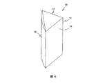
図4は本発明の他の実施形態を示す。図4を参照すれば、電磁波ビーム42の光源41はビーム42を基板46上に形成された被覆44へ導く。反射光学系40は、被覆44と基板46を透過した監視ビーム45を反射し、基板および被覆を通って検出器48へ戻るように配置される。
FIG. 4 shows another embodiment of the present invention. Referring to FIG. 4, the
このシステムのひとつの利点は、検出器48によって受け取られた反射ビーム47の信号対ノイズ特性が改善されることである。監視ビームは、ビームの所望の特性を測定する前に被覆と基板を通って2度透過することにより、総透過率は二乗され、ノイズは一定に近く維持される。したがって、被覆の光学特性の変化による透過率の実際の変化をシステムの中でノイズから識別することが容易である。
One advantage of this system is that the signal to noise characteristics of the reflected
一実施形態において、反射光学系は逆反射体、すなわち反射された光線が入射光線の方向とは実質上反対方向に戻される反射器を含む。図5を参照すれば、逆反射体50は、直角プリズムの斜辺を形成する実質上垂直な面52、54、56を有する、細長い直角プリズム51を含むことができる。逆反射体は被覆と基板を透過した監視ビームが面56に入射し、実質上垂直な面52および54によって逆反射されるように配置される。入射ビームの逆反射は、面52、54の内部反射に完全に依存することができる。代りに、反射被覆を面52、54に塗工することができる。
In one embodiment, the reflective optics includes a retroreflector, i.e., a reflector in which the reflected light beam is returned in a direction substantially opposite to the direction of the incident light beam. Referring to FIG. 5, the
図6を参照すれば、平凸レンズ58を面56に隣接して配置することができる。レンズの焦点距離は、入射ビームが面56をプリズム中に通過するとき平行になるように選択される。
Referring to FIG. 6, a plano-
図7を参照すれば、図6に示した逆反射体50を用いる本発明の一実施形態において、光源60および検出器62の軸は実質上同一平面上にあり、軸を含む面は、直角プリズム51の実質上垂直な面52、54で形成される縁部53に実質上平行である。それらの構成において、光源と検出器の軸を含む面に垂直方向の構成要素の光学的配列は逆反射体の逆反射特性のため自動的である。したがって、構成要素の光学配列は光源と検出器の軸の面内でのみ重要である。それらのシステムの光学配列は、逆反射器を用いないシステムよりも単純化され、検出器での監視信号の損失によって塗工工程が妨げられる可能性を最小にする。
Referring to FIG. 7, in one embodiment of the present invention using the
本発明の光学監視システムは、基板がビーム源を過ぎて移動する際に監視ビームの入射角度が変化する塗工システムの光学的監視の改善に特に有益である。それらのシステムのひとつは、Bartolomeiらが開示したドラム式スパッタ塗工システムである。Bartolomeiらが開示した装置および工程などのスパッタ堆積装置および工程に、堆積された被覆の光学特性の関数として工程制御を組み込むためには、いくつかの要因を考慮しなければならない。層を堆積してBartolomeiらが開示したような多層薄膜被覆を形成する典型的な塗工工程において、ドラムは約0.6から1メートルの直径を有し、約1rpmで回転する。基板サイズが約2インチであると仮定すれば、基板は静止した監視ビームの前を約20msで通過するであろう。したがって、通過ごとに光学データを集めるには非常に僅かな時間しかない。工程は、基板を横断する被覆の不均一性のため、および通過中約3°から4°であるドラムの湾曲によって通過中に監視ビームの基板への入射角度が変化するため、さらに複雑である。 The optical monitoring system of the present invention is particularly useful for improving the optical monitoring of coating systems in which the angle of incidence of the monitoring beam changes as the substrate moves past the beam source. One of those systems is the drum-type sputter coating system disclosed by Bartolomei et al. In order to incorporate process control as a function of the optical properties of the deposited coating into a sputter deposition apparatus and process, such as the apparatus and process disclosed by Bartolomei et al., Several factors must be considered. In a typical coating process where the layers are deposited to form a multilayer thin film coating as disclosed by Bartolomei et al., The drum has a diameter of about 0.6 to 1 meter and rotates at about 1 rpm. Assuming the substrate size is about 2 inches, the substrate will pass in front of a stationary monitoring beam in about 20 ms. Therefore, there is very little time to collect optical data for each pass. The process is more complicated because of the non-uniformity of the coating across the substrate and because the angle of incidence of the monitoring beam on the substrate changes during the passage due to the curvature of the drum, which is about 3 ° to 4 ° during the passage. .
それらのシステムにおいて、被覆の特性を測定するために監視ビームの入射角度は基板の面に垂直である必要はないので、逆反射体を使用すると、基板が監視点を通過する各通過中に基板上の被覆の光学特性を測定するために用いられる時間が最大化される。図8を参照すれば、基板搬送器70は、光源74と検出器76の位置が固定されている監視点71を過ぎて基板72を搬送する。光源74と検出器76の軸は同一平面上にあり、軸を含む面は実質上逆反射器50の長軸に平行であり、監視点を過ぎて移動する基板72の速度に実質上垂直である。図示したように、監視ビーム75は、基板72が監視点71を過ぎて矢方向に移動する際、実質上基板72に垂直である。全体的に円筒状の基板搬送器70(すなわちドラム)の湾曲(図示されない)のため、基板がビーム源を通過する際、基板へのビームの入射角度は変化する。しかし、逆反射体50の逆反射特性のため、システムは、基板に対してビームが垂直である位置に基板が接近し離れる際に、基板に対して直角以外の角度で基板を透過した、逆反射されたビームを受け取ることが可能である。したがって、基板上に形成された被覆の光学特性を監視するために用いられる時間は逆反射体の使用によって増加する。
In these systems, the angle of incidence of the monitoring beam need not be perpendicular to the plane of the substrate in order to measure the properties of the coating, so using a retroreflector allows the substrate to pass through each pass through the monitoring point. The time used to measure the optical properties of the top coating is maximized. Referring to FIG. 8, the
一実施形態において、反射光学系は反射器の位置が基板に対して固定されるように、基板搬送器(例えば、ドラムまたは円板)によって搬送することができる。この実施形態において、必要に応じて多くの基板をアレー中で測定し、工程制御とアレー中の被覆の均一性を改善することができる。 In one embodiment, the reflective optics can be transported by a substrate transporter (eg, a drum or disc) such that the position of the reflector is fixed relative to the substrate. In this embodiment, as many substrates as required can be measured in the array to improve process control and coating uniformity in the array.
本発明の一態様において、堆積されている膜の光学特性の関数として堆積が停止されおよび/または制御されるスパッタ堆積工程で基板上に薄膜を堆積する装置および方法が開示される。一実施形態において、膜の望ましい厚さを求めるために、所望の波長を有する電磁波ビームの薄膜を通る透過性が測定される。工程は、
基板をドラム表面に搭載するステップと、
ドラムを回転し、それによって基板のアレーを1個または複数の堆積すべき材料源を過ぎて搬送し、それによって基板上の材料の堆積を実施するステップと、
基板およびその表面上に堆積された被覆を通して、ドラムの各回転中少なくとも1回電磁波ビームを導くステップと、
基板と被覆を通ったビームの透過率を測定するステップと、
基板と被覆を通ったビームの透過率の関数として材料の堆積を停止するステップとを含むことができる。
In one aspect of the invention, an apparatus and method for depositing a thin film on a substrate in a sputter deposition process in which deposition is stopped and / or controlled as a function of the optical properties of the deposited film is disclosed. In one embodiment, the permeability of an electromagnetic beam having a desired wavelength through a thin film is measured to determine the desired thickness of the film. The process is
Mounting the substrate on the drum surface;
Rotating the drum, thereby transporting the array of substrates past the source of material or materials to be deposited, thereby performing the deposition of material on the substrate;
Directing the electromagnetic beam through the substrate and the coating deposited on its surface at least once during each rotation of the drum;
Measuring the transmittance of the beam through the substrate and the coating;
Stopping deposition of the material as a function of the transmittance of the beam through the substrate and the coating.
一実施形態は、予め選択された波長λcの反射、吸収、または透過率を有する光学フィルター中の層を製造する装置であり、装置は、
その上に基板を搭載した回転可能なドラム(円板)と、
1個または複数のスパッタターゲットと、
ドラムの一方の側に配置され、ドラムの回転中に基板を通過するように配置された、所望の波長を有するレーザー(レーザーは所望の波長または白光源に調整した短時間調整レーザーとすることができる)と、
レーザーの反対側のドラム(円板)側部に配置され、基板を通るレーザーの透過率を測定するように配置された監視器と、
材料の堆積を停止する工程中の望ましい点を求めるためのコンピュータであって、
基板の通過ごとに監視器のデータ出力を集合し集積すること、
統計的なノイズをフィルターで除去すること、
監視器のビームの入射角度、表面のスピン、回転、または不均一性、基板の揺れまたは他の動き、入射角度および反射され透過したまたは吸収された波長の変動、基板および膜スタックの温度変化を補正しまたは補償すること、
強度カーブを数学的にモデル化すること、
λもしくは他の波長で所望の透過率に到達する時間、サイクル数、または監視レベルを計算すること、
基板の各通過または選択された通過ごとに、監視器を通してAからFの繰り返しに基づいてモデル化されたカーブを再計算すること、のひとつまたは複数を実行することができるコンピュータと、
所望の予め選択された光学特性が得られたときに堆積を終了する手段、または、
最適堆積のために予測した時間、サイクル数、または監視器の読み取りに達したときに堆積を終了する手段、または、
予め選択された反応終点で所望の光学特性が得られるように、反応因子を調節して堆積速度を変更する手段とを含むことができる。
One embodiment is an apparatus for producing a layer in an optical filter having reflection, absorption, or transmission at a preselected wavelength λc, the apparatus comprising:
A rotatable drum (disc) with a substrate mounted on it,
One or more sputter targets;
A laser with a desired wavelength placed on one side of the drum and passing through the substrate during the rotation of the drum (the laser may be a short-time tuned laser adjusted to the desired wavelength or white light source) Can)
A monitor located on the drum (disc) side opposite the laser and arranged to measure the transmission of the laser through the substrate;
A computer for determining a desired point in the process of stopping material deposition,
Collecting and accumulating the data output of the monitor as each board passes,
Filtering out statistical noise,
Monitor beam incidence angle, surface spin, rotation, or inhomogeneity, substrate shaking or other movement, incidence angle and reflected or absorbed wavelength variation, substrate and film stack temperature changes Correct or compensate,
Mathematically modeling the intensity curve,
calculating the time to reach the desired transmission at λ or other wavelengths, the number of cycles, or the monitoring level;
A computer capable of performing one or more of recalculating the modeled curve based on the iterations of A to F through the monitor for each or each selected pass of the substrate;
Means for terminating the deposition when the desired preselected optical properties are obtained, or
Means to terminate deposition when the estimated time, cycle number, or monitor reading for optimal deposition is reached, or
Means for adjusting the reaction factors to change the deposition rate so that the desired optical properties are obtained at a preselected reaction endpoint.
堆積反応の終点の実時間計算を用いて、予め選択された波長λcの反射、吸収、または透過率を有する光学フィルター中の層を製造する方法は、
(f)波長λcのレーザー(または短時間調整レーザー)を反応性スパッタ塗工工程の間基板に導くこと、
(g)ビームが光学膜を通過しまたは反射された後に、光学監視器でビームの強度を測定すること、
(h)監視器のデータ出力を用いて、層の最大または最小の透過、反射または吸収を数学的にモデル化すること、
(i)最大または最小の透過、反射または吸収に達したとき堆積を停止し、またはその光学膜の厚さについて予測した時間に達したとき堆積を停止することとを含むことができる。
代りに、白色光を基板に導き、対象の波長で光の強度を測定することができる。
堆積反応の終点の実時間監視および実時間フィードバック反応条件調節を用いて、予め選択された波長λの反射、吸収、または透過率を有する光学フィルター中の層を製造するさらに他の方法は、
(a)基板を周期的に1種または複数種のスパッタターゲットを通過させることによって基板上に1種または複数種の材料をスパッタ堆積すること、
(b)所望波長または複数の所望波長の電磁波ビームを提供すること、
(c)ビームが実質上基板表面に垂直になるように、ビームに基板を通過させること、
(d)基板およびその上の被覆によって反射され、吸収され、または透過したビームのエネルギーを測定し記録すること、
(e)監視器によって集められたデータを解析しモデル化して、被覆された基板の所望の光学特性を得るために調節すべき、
A)ターゲット電圧、
B)ターゲットと基板間の距離、
C)ドラム(円板)の回転速度とを含むが制限されない反応因子または複数の因子を求めること、
(f)フィードバック系によってモデルを連続的に更新し、反応条件を調節することとを含むことができる。
Using a real-time calculation of the endpoint of the deposition reaction, a method for producing a layer in an optical filter having reflection, absorption, or transmission at a preselected wavelength λc is as follows:
(F) directing a laser of wavelength λc (or a short-time tuning laser) to the substrate during the reactive sputter coating process;
(G) measuring the intensity of the beam with an optical monitor after the beam has passed or reflected through the optical film;
(H) mathematically modeling the maximum or minimum transmission, reflection or absorption of the layer using the data output of the monitor;
(I) stopping the deposition when maximum or minimum transmission, reflection or absorption is reached, or stopping the deposition when the expected time for the thickness of the optical film is reached.
Alternatively, white light can be directed to the substrate and the light intensity measured at the wavelength of interest.
Yet another method of producing a layer in an optical filter having a reflection, absorption, or transmission of a preselected wavelength λ using real-time monitoring of the endpoint of the deposition reaction and real-time feedback reaction condition adjustment includes:
(A) sputter depositing one or more materials on the substrate by periodically passing the substrate through one or more sputter targets;
(B) providing an electromagnetic beam having a desired wavelength or a plurality of desired wavelengths;
(C) passing the beam through the substrate so that the beam is substantially perpendicular to the substrate surface;
(D) measuring and recording the energy of the beam reflected, absorbed or transmitted by the substrate and the coating thereon;
(E) the data collected by the monitor should be analyzed and modeled to adjust to obtain the desired optical properties of the coated substrate;
A) Target voltage,
B) Distance between target and substrate,
C) determining a reaction factor or factors including but not limited to the rotational speed of the drum (disk);
(F) continuously updating the model with a feedback system and adjusting the reaction conditions.
本発明の好ましい実施形態を説明したが、説明した実施形態は例示のためだけであり、本発明の範囲は、等価のものの全範囲に一致するとき、添付された請求項によって完全に定義され、当業者であれば、その吟味から多くの変形と修正を自然に想起するであろうことを理解すべきである。 While preferred embodiments of the invention have been described, the described embodiments are for illustration purposes only, the scope of the invention is fully defined by the appended claims, and is consistent with the full scope of equivalents, It should be understood that those skilled in the art will naturally recall many variations and modifications from their review.
Claims (18)
前記基板搬送器に、前記基板の被覆の反対側に位置されるように前記反射器が固定されている請求項1〜6のいずれか1項に記載の光学特性監視システム。The optical property monitoring system according to any one of claims 1 to 6, wherein the reflector is fixed to the substrate transporter so as to be positioned on an opposite side of the coating of the substrate.
電磁波ビームを前記基板及び前記被覆を透過するように前記基板に入射させるステップと、 Incident an electromagnetic wave beam on the substrate so as to pass through the substrate and the coating;
前記基板及び前記被覆を透過した電磁波ビームを逆反射させてこの前記基板及び前記被覆を再度透過するように導く逆反射のステップと、 Retroreflecting a step of retroreflecting an electromagnetic wave beam transmitted through the substrate and the coating to guide the electromagnetic beam again through the substrate and the coating;
逆反射して前記基板及び前記被覆を透過した電磁波ビームの選択された特性を測定するステップと、 Measuring selected characteristics of an electromagnetic wave beam that is retroreflected and transmitted through the substrate and the coating;
前記被覆の選択された光学特性を求めるステップとを備えたことを特徴とする監視方法。 Determining a selected optical property of the coating.
Applications Claiming Priority (3)
| Application Number | Priority Date | Filing Date | Title |
|---|---|---|---|
| US53650004P | 2004-01-15 | 2004-01-15 | |
| US60/536,500 | 2004-01-15 | ||
| PCT/US2005/001666 WO2005071134A1 (en) | 2004-01-15 | 2005-01-18 | Method and apparatus for monitoring optical characteristics of thin films in a deposition process |
Publications (2)
| Publication Number | Publication Date |
|---|---|
| JP2007522342A JP2007522342A (en) | 2007-08-09 |
| JP4904165B2 true JP4904165B2 (en) | 2012-03-28 |
Family
ID=34807015
Family Applications (1)
| Application Number | Title | Priority Date | Filing Date |
|---|---|---|---|
| JP2006549694A Expired - Fee Related JP4904165B2 (en) | 2004-01-15 | 2005-01-18 | Method and apparatus for monitoring optical properties of thin films during a deposition process |
Country Status (4)
| Country | Link |
|---|---|
| US (1) | US7008518B2 (en) |
| EP (1) | EP1711645B1 (en) |
| JP (1) | JP4904165B2 (en) |
| WO (1) | WO2005071134A1 (en) |
Families Citing this family (21)
| Publication number | Priority date | Publication date | Assignee | Title |
|---|---|---|---|---|
| US7068430B1 (en) * | 2003-05-06 | 2006-06-27 | Semrock, Inc. | Method of making highly discriminating optical edge filters and resulting products |
| US7119960B1 (en) * | 2003-05-06 | 2006-10-10 | Semrock, Inc. | Method of making high performance optical edge and laser-line filters and resulting products |
| US7889346B2 (en) | 2003-12-31 | 2011-02-15 | University Of South Carolina | Thin-layer porous optical sensors for gases and other fluids |
| US20070201136A1 (en) * | 2004-09-13 | 2007-08-30 | University Of South Carolina | Thin Film Interference Filter and Bootstrap Method for Interference Filter Thin Film Deposition Process Control |
| US8345234B2 (en) | 2005-11-28 | 2013-01-01 | Halliburton Energy Services, Inc. | Self calibration methods for optical analysis system |
| WO2007061437A1 (en) | 2005-11-28 | 2007-05-31 | University Of South Carolina | Optical analysis system for dynamic, real-time detection and measurement |
| EP1969326B1 (en) | 2005-11-28 | 2020-06-10 | Ometric Corporation | Optical analysis system and method for real time multivariate optical computing |
| US20070166245A1 (en) | 2005-11-28 | 2007-07-19 | Leonard Mackles | Propellant free foamable toothpaste composition |
| WO2008002903A2 (en) | 2006-06-26 | 2008-01-03 | University Of South Carolina | Data validation and classification in optical analysis systems |
| US9182282B2 (en) | 2006-11-02 | 2015-11-10 | Halliburton Energy Services, Inc. | Multi-analyte optical computing system |
| US20080121513A1 (en) * | 2006-11-24 | 2008-05-29 | Tdk Corporation | Processing condition obtaining method and thin-film forming method |
| WO2008121684A1 (en) * | 2007-03-30 | 2008-10-09 | University Of South Carolina | Novel multi-analyte optical computing system |
| US8212216B2 (en) | 2007-03-30 | 2012-07-03 | Halliburton Energy Services, Inc. | In-line process measurement systems and methods |
| US8184295B2 (en) | 2007-03-30 | 2012-05-22 | Halliburton Energy Services, Inc. | Tablet analysis and measurement system |
| US8283633B2 (en) * | 2007-11-30 | 2012-10-09 | Halliburton Energy Services, Inc. | Tuning D* with modified thermal detectors |
| US8212213B2 (en) | 2008-04-07 | 2012-07-03 | Halliburton Energy Services, Inc. | Chemically-selective detector and methods relating thereto |
| KR20090109375A (en) * | 2008-04-15 | 2009-10-20 | 삼성전자주식회사 | Method for controling thin film forming velocity, thin film forming method having the method and thin film forming system for performing the thin film forming method |
| CN102152541B (en) * | 2010-12-10 | 2013-11-20 | 厦门建霖工业有限公司 | Method for preparing composite interlayer coating film on surface of engineering plastics |
| CN103384811B (en) * | 2012-02-15 | 2014-11-26 | 株式会社新柯隆 | Optical film thickness measurement apparatus and thin-film forming apparatus using optical film thickness measurement apparatus |
| JP6243660B2 (en) * | 2013-08-21 | 2017-12-06 | Hoya株式会社 | Mask blank manufacturing method and transfer mask manufacturing method |
| US20220349088A1 (en) * | 2021-04-28 | 2022-11-03 | Applied Materials, Inc. | In-situ film growth rate monitoring apparatus, systems, and methods for substrate processing |
Citations (6)
| Publication number | Priority date | Publication date | Assignee | Title |
|---|---|---|---|---|
| JPS54119948A (en) * | 1978-03-10 | 1979-09-18 | Asahi Dow Ltd | Method and device for measuring thickness of infrared multilayer film |
| JPS6189542A (en) * | 1984-09-24 | 1986-05-07 | コルモーゲン コーポレイション | Method of simultaneously measuring thickness and orientationof polymerized film |
| US5546179A (en) * | 1994-10-07 | 1996-08-13 | Cheng; David | Method and apparatus for mapping the edge and other characteristics of a workpiece |
| JPH08315432A (en) * | 1995-05-15 | 1996-11-29 | Nippondenso Co Ltd | Apparatus for producing optical information recording medium and production method therefor |
| WO2002050501A1 (en) * | 2000-12-19 | 2002-06-27 | Kla-Tencor Corporation | Parametric profiling using optical spectroscopic systems |
| WO2002063064A1 (en) * | 2001-02-07 | 2002-08-15 | Asahi Glass Company, Limited | Spatter device and spatter film forming method |
Family Cites Families (10)
| Publication number | Priority date | Publication date | Assignee | Title |
|---|---|---|---|---|
| GB2016678B (en) * | 1978-03-10 | 1982-09-15 | Asahi Dow Ltd | Infrared multilayer film thickness measuring method and apparatus |
| DE3378508D1 (en) | 1982-09-10 | 1988-12-22 | Nippon Telegraph & Telephone | Plasma deposition method and apparatus |
| US4851095A (en) | 1988-02-08 | 1989-07-25 | Optical Coating Laboratory, Inc. | Magnetron sputtering apparatus and process |
| DE3920835C2 (en) | 1989-06-24 | 1997-12-18 | Leybold Ag | Device for coating substrates |
| DE4106770C2 (en) | 1991-03-04 | 1996-10-17 | Leybold Ag | Performing reactive coating of a substrate |
| ES2093133T3 (en) | 1991-04-12 | 1996-12-16 | Balzers Hochvakuum | PROCEDURE AND INSTALLATION FOR THE COATING OF AT LEAST ONE OBJECT. |
| US5849162A (en) | 1995-04-25 | 1998-12-15 | Deposition Sciences, Inc. | Sputtering device and method for reactive for reactive sputtering |
| US5756369A (en) * | 1996-07-11 | 1998-05-26 | Lsi Logic Corporation | Rapid thermal processing using a narrowband infrared source and feedback |
| FR2796462B1 (en) * | 1999-07-15 | 2001-09-07 | Eastman Kodak Co | METHOD AND DEVICE FOR DETECTING A DEFECT IN A LIQUID TABLECLOTH |
| US6911349B2 (en) * | 2001-02-16 | 2005-06-28 | Boxer Cross Inc. | Evaluating sidewall coverage in a semiconductor wafer |
-
2005
- 2005-01-18 EP EP05722465.1A patent/EP1711645B1/en not_active Not-in-force
- 2005-01-18 US US11/036,326 patent/US7008518B2/en active Active
- 2005-01-18 JP JP2006549694A patent/JP4904165B2/en not_active Expired - Fee Related
- 2005-01-18 WO PCT/US2005/001666 patent/WO2005071134A1/en active Application Filing
Patent Citations (6)
| Publication number | Priority date | Publication date | Assignee | Title |
|---|---|---|---|---|
| JPS54119948A (en) * | 1978-03-10 | 1979-09-18 | Asahi Dow Ltd | Method and device for measuring thickness of infrared multilayer film |
| JPS6189542A (en) * | 1984-09-24 | 1986-05-07 | コルモーゲン コーポレイション | Method of simultaneously measuring thickness and orientationof polymerized film |
| US5546179A (en) * | 1994-10-07 | 1996-08-13 | Cheng; David | Method and apparatus for mapping the edge and other characteristics of a workpiece |
| JPH08315432A (en) * | 1995-05-15 | 1996-11-29 | Nippondenso Co Ltd | Apparatus for producing optical information recording medium and production method therefor |
| WO2002050501A1 (en) * | 2000-12-19 | 2002-06-27 | Kla-Tencor Corporation | Parametric profiling using optical spectroscopic systems |
| WO2002063064A1 (en) * | 2001-02-07 | 2002-08-15 | Asahi Glass Company, Limited | Spatter device and spatter film forming method |
Also Published As
| Publication number | Publication date |
|---|---|
| JP2007522342A (en) | 2007-08-09 |
| WO2005071134A1 (en) | 2005-08-04 |
| US20050167264A1 (en) | 2005-08-04 |
| EP1711645B1 (en) | 2013-12-25 |
| EP1711645A1 (en) | 2006-10-18 |
| US7008518B2 (en) | 2006-03-07 |
| EP1711645A4 (en) | 2007-12-19 |
Similar Documents
| Publication | Publication Date | Title |
|---|---|---|
| JP4904165B2 (en) | Method and apparatus for monitoring optical properties of thin films during a deposition process | |
| US7123416B1 (en) | Method of making high performance optical edge and notch filters and resulting products | |
| US10522375B2 (en) | Monitoring system for deposition and method of operation thereof | |
| US4582431A (en) | Optical monitor for direct thickness control of transparent films | |
| US7345765B2 (en) | Optical monitoring of thin films using fiber optics | |
| US7068430B1 (en) | Method of making highly discriminating optical edge filters and resulting products | |
| CN113403601B (en) | Optical control device and method for coating thickness | |
| CN102472611B (en) | Optical film thickness meter and thin film forming apparatus provided with optical film thickness meter | |
| EP0585883B1 (en) | Method of measuring refractive index of thin film | |
| Starke et al. | Rapid prototyping of optical thin film filters | |
| US11466362B2 (en) | Apparatus and methods for depositing durable optical coatings | |
| US8200448B2 (en) | Optical monitor for rugate filter deposition | |
| EP1148149B1 (en) | Method for the production of multi-layer systems | |
| US7176474B2 (en) | Method and apparatus for measuring and monitoring coatings | |
| JP2021031693A (en) | Optical film thickness control device, thin film formation device, optical film thickness control method, and thin film formation method | |
| JP7240321B2 (en) | Methods of assembling optical systems and minimizing distortion due to retardance in optical assemblies | |
| JPH11162954A (en) | Method and equipment for measuring thin film by optical means and film formation equipment | |
| US20070019204A1 (en) | Spectrometer based multiband optical monitoring of thin films | |
| RU2158897C1 (en) | Method testing thickness of film in process of its deposition and device for its realization | |
| CN117248178A (en) | Film plating device and film plating method for monitoring surface shape of lens in real time | |
| RU2075727C1 (en) | Method of measurement of angles of turn of several objects and device for its implementation | |
| US20080151245A1 (en) | method and a device for processing birefringent and/or optically active materials and phase plate | |
| CN117305796A (en) | Film plating device and film plating method for monitoring refractive index in real time | |
| Vol'pyan et al. | Analysis of errors in the photometric monitoring of layer thickness | |
| Zoeller et al. | Direct optical monitoring enables high performance applications in mass production |
Legal Events
| Date | Code | Title | Description |
|---|---|---|---|
| A621 | Written request for application examination |
Free format text: JAPANESE INTERMEDIATE CODE: A621 Effective date: 20080110 |
|
| A131 | Notification of reasons for refusal |
Free format text: JAPANESE INTERMEDIATE CODE: A131 Effective date: 20110426 |
|
| A521 | Request for written amendment filed |
Free format text: JAPANESE INTERMEDIATE CODE: A523 Effective date: 20110719 |
|
| TRDD | Decision of grant or rejection written | ||
| A01 | Written decision to grant a patent or to grant a registration (utility model) |
Free format text: JAPANESE INTERMEDIATE CODE: A01 Effective date: 20111220 |
|
| A01 | Written decision to grant a patent or to grant a registration (utility model) |
Free format text: JAPANESE INTERMEDIATE CODE: A01 |
|
| A61 | First payment of annual fees (during grant procedure) |
Free format text: JAPANESE INTERMEDIATE CODE: A61 Effective date: 20120106 |
|
| R150 | Certificate of patent or registration of utility model |
Free format text: JAPANESE INTERMEDIATE CODE: R150 |
|
| FPAY | Renewal fee payment (event date is renewal date of database) |
Free format text: PAYMENT UNTIL: 20150113 Year of fee payment: 3 |
|
| LAPS | Cancellation because of no payment of annual fees |