EP0585883B1 - Method of measuring refractive index of thin film - Google Patents
Method of measuring refractive index of thin film Download PDFInfo
- Publication number
- EP0585883B1 EP0585883B1 EP93113919A EP93113919A EP0585883B1 EP 0585883 B1 EP0585883 B1 EP 0585883B1 EP 93113919 A EP93113919 A EP 93113919A EP 93113919 A EP93113919 A EP 93113919A EP 0585883 B1 EP0585883 B1 EP 0585883B1
- Authority
- EP
- European Patent Office
- Prior art keywords
- thin film
- refractive index
- substrate
- light
- measuring
- Prior art date
- Legal status (The legal status is an assumption and is not a legal conclusion. Google has not performed a legal analysis and makes no representation as to the accuracy of the status listed.)
- Expired - Lifetime
Links
Images


Classifications
-
- G—PHYSICS
- G01—MEASURING; TESTING
- G01N—INVESTIGATING OR ANALYSING MATERIALS BY DETERMINING THEIR CHEMICAL OR PHYSICAL PROPERTIES
- G01N21/00—Investigating or analysing materials by the use of optical means, i.e. using sub-millimetre waves, infrared, visible or ultraviolet light
- G01N21/17—Systems in which incident light is modified in accordance with the properties of the material investigated
- G01N21/41—Refractivity; Phase-affecting properties, e.g. optical path length
-
- G—PHYSICS
- G01—MEASURING; TESTING
- G01N—INVESTIGATING OR ANALYSING MATERIALS BY DETERMINING THEIR CHEMICAL OR PHYSICAL PROPERTIES
- G01N21/00—Investigating or analysing materials by the use of optical means, i.e. using sub-millimetre waves, infrared, visible or ultraviolet light
- G01N21/84—Systems specially adapted for particular applications
- G01N21/8422—Investigating thin films, e.g. matrix isolation method
Definitions
- the present invention relates to a method of measuring the refractive index of a dielectric film, and more particularly to a method of measuring the refractive index of a dielectric thin film during the formation thereof in a thin film formation apparatus such as a vacuum deposition apparatus and a sputtering apparatus.
- the refractive index of a thin film formed is not necessarily the same as the refractive index of a bulk of the thin film, and usually varies depending upon the deposition conditions and other conditions in the deposition atmosphere during the formation thereof.
- optical constants such as the thickness of a thin film formed by vacuum deposition on the spot during the formation of the thin film, by an optical film thickness meter, until a maximum interference value of the thin film is obtained after starting the deposition of the thin film.
- the film thickness that can be measured is the optical film thickness (nd), so that it is impossible to measure optical constants of an extremely thin film, particularly on the spot during the formation thereof.
- the object of the present invention can be attained by a method comprising the steps of (a) forming a dielectric thin film which is transparent, uniform and geometrically and optically identical, on each of a first substrate and a second substrate, with the refractive indexes of the first substrate and the second substrate being different; and (b) measuring the reflectivities of the first and second substrates, each bearing the dielectric thin film thereon, with the application of a light with an identical wavelength to the two substrates, thereby measuring the refractive index of the dielectric thin film on the spot during the formation of the dielectric thin film.
- the method of the present invention can be carried out employing a refractive index measuring apparatus which comprises a thickness measuring optical system for sequentially guiding a luminous flux emitted from a light source to a first monitor substrate and a second monitor substrate on both of which a dielectric thin film is to be formed, and then guiding two light rays respectively reflected by the first and second monitor substrates to light receiving means; and operation means for calculating the refractive index of the dielectric thin film from two intensity signals from the light receiving means.
- a refractive index measuring apparatus which comprises a thickness measuring optical system for sequentially guiding a luminous flux emitted from a light source to a first monitor substrate and a second monitor substrate on both of which a dielectric thin film is to be formed, and then guiding two light rays respectively reflected by the first and second monitor substrates to light receiving means; and operation means for calculating the refractive index of the dielectric thin film from two intensity signals from the light receiving means.
- the refractive index measuring apparatus if a reference light for correcting the intensity of the light flux from the light source, and a dark light for correcting a stray light which enters the light receiving means, and also for correcting the circuits for the light receiving means are led to the light receiving means while the light reflected by the first monitor substrate and the light reflected by the second monitor substrate are sequentially measured, the refractive index of the thin film can be easily measured and controlled on the spot during the fabrication of the thin film.
- a thin film with a refractive index n and a geometrical film thickness d i.e., a thin film with an optical film thickness nd
- the reflectivity Rg 1 of one of the two monitor substrates and the reflectivity Rg 2 of the other monitor substrate are measured by applying a light with an identical wavelength ⁇
- the refractive index n and the geometrical film thickness d of the thin film can be obtained.
- the refractive index n and the geometrical film thickness d of the thin film can be obtained from the following Equation (2) by measuring the two reflectivities Rg 1 and Rg 2 :
- X 2 ⁇ G 1 ⁇ G 2 ( G 2 ⁇ E 1 ⁇ D 2 - G 1 ⁇ D 1 ⁇ E 2 )+ D 1 ⁇ D 2 ( G 2 2 - G 2 1 ) 2( G 1 ⁇ E 1 ⁇ D 2 - G 2 ⁇ D 1 ⁇ E 2 )- D 1 ⁇ D 2 ( G 2 2 - G 2 1 )
- X is n 2 , wherein n is the refractive index of the thin film, G 1 is the refractive index ns 1 of the first substrate, G 2 is the refractive index ns 2 of the second substrate, Rg 1 is the refractivity of the first substrate when a thin film with an optical film thickness nd is deposited thereon, Rg 2 is the refractivity of the second substrate when a thin film with an optical film
- the reflectivity Rg 1 and the reflectivity Rg 2 be respectively determined as an absolute intensity in the form of a ratio of incident light intensity/reflected light intensity.
- a reference substrate with a known refractive index, which is chemically stable, such as a quartz substrate it is necessary to use a reference substrate with a known refractive index, which is chemically stable, such as a quartz substrate, and to obtain the correlation between the reflected light quantity and the reflectivity thereof to be measured.
- a dielectric thin film is deposited, for instance, by vacuum deposition, on the surface of each of two transparent substrates made of an optical glass with a known refractive index serving as the first and second monitor substrates, so that the reflectivity of the back side of each substrate can be measured during the formation of the dielectric thin film by vacuum deposition.
- a thin film with a predetermined refractive index can be formed by controlling the conditions for the film formation, such as the deposition (sputtering) rate, the temperature of the substrates, and partial gas pressures in the atmosphere for the deposition (in the case of reactive deposition, and reactive sputtering), so as to make up for the deviation of the predetermined value of the refractive index.
- Equation (2) The calculation of the refractive index of a thin film by use of the previously mentioned Equation (2) will now be explained more specifically.
- Fig. 1 is a diagram in explanation of an example of a refractive index measuring apparatus according to the present invention.
- a deposition source 17 for controlling the ejection of a deposition material to be deposited from the deposition source 17, a substrate holder 13 for holding a substrate onto which the deposition material is to be deposited, and a heater 15 for heating the substrate.
- a monitor glass which is composed of a monitor glass substrate 51A and a monitor glass substrate 53B for monitoring the refractive index and thickness of a thin film to be formed on the substrate by vacuum deposition.
- Fig. 3 is a plain view of the monitor glass substrate which is composed of the monitor glass substrate 51A and the monitor glass substrate 53B.
- the refractive indexes of the two monitor glass substrates 51A and 53B are different.
- the vacuum chamber 11 is also provided with a gas cylinder 21 for introducing a gas such as oxygen into the vacuum chamber 11, a variable valve 23 for controlling the amount of the gas to be introduced into the vacuum chamber 11, and a transparent monitoring window 12 made of a glass.
- a collimator luminous flux emitted from the light source 31 is reflected by the scanning mirror 35, passes through the half-mirror 41, the lens 43, and the monitoring window 12, and projected in the shape of a spot on the monitor glass substrate 51A or 53B.
- the light is then reflected by the monitor glass substrate 51A or 53B, passes through the monitoring window 12 and the lens 43, and is then reflected by the half-mirror 41.
- the light reflected by the half-mirror 41 is then led to a light receiving unit 47 through the interference filter 45 with a transmission center wavelength ⁇ , so that the intensity of the reflected light is measured.
- the luminous flux from the light source 31 passes through the scanning mirror 35 and directly enters the light receiving unit 47 through mirrors 37, 39 and the half-mirror 41.
- the wavelength ⁇ of the light for the measurement of the light can be set as desired by the interference filter 45.
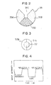
- the scanning mirror 35 is segmented into four zones as illustrated in a plain view thereof in Fig. 2. More specifically, the scanning mirror 35 is composed of high reflection mirror sections 35A and 35B with an aluminum film deposited thereon, an opaque, non-reflecting section 35D which minimizes the reflection and transmission of the luminous flux emitted from the light source 31, for instance, by applying thereto a back coating, and a cut-away section 35C, which is cut away from the scanning mirror 35 in order to prevent any and all reflection by the scanning mirror 35.
- the reflection characteristics of the high reflection mirror sections 35A and 35B are made identical.
- a transparent section without any deposition thereon or with an antireflection film can be formed in the scanning mirror 35.
- the scanning mirror 35 is fixed to a rotary shaft of a scanning motor 33, with an angle deviating from a right angle to the rotary shaft.
- the angle between the scanning mirror 35 and the luminous flux emitted from the light source 31 varies during the rotation of the scanning mirror 35, so that a light spot 32 formed on the monitor glass substrates 51A and 53B by the light reflected from the scanning mirror 35 makes a circular motion as shown by the arrow in Fig. 3.
- the luminous flux reflected by the high reflection mirror section 35A of the rotating scanning mirror 35 is projected on the monitor glass substrate 51A, while the luminous flux reflected by the high reflection mirror section 35B is projected on the monitor glass 53B.
- the monitor glass substrates 51A and 53B are stationary.
- signals are input to the light receiving unit 47 in the order of (a) reference (a luminous flux passed through the cut-away portion 35C), (b) reflection A (reflection light from the monitor glass 51A), (c) dark (light which is inevitably reflected by the opaque, non-reflecting section 35D, and reflected by an intermediate area between the monitor glass substrate 51A and the monitor glass substrate 53B, which is an extremely slight reflection light, ideally with a zero input signal), and (d) reflection B (reflection light from the monitor glass 53B).
- the intensity of the reference is determined depending upon the reflectivities of the mirrors 37 and 39, and the transmittance of the half-mirror 41. Therefore, the reference can be used as a reference light with a fixed intensity for correcting the intensity of the light from the light source 31. Furthermore, the reference can be used as a signal light for distinguishing between the reflection A and the reflection B.
- the dark with a substantially zero input signal can be used to correct the stray light and the circuits of the light receiving unit.
- the dark is also used as a signal light for distinguishing between the reflection A and the reflection B.
- n is the refractive index
- d is the geometrical thickness
- the refractive index n of the dielectric thin film can be calculated on the spot by a computer 25 (arithmetic unit), and the calculated refractive index n can be displayed on a display unit 27.
- the refractive index When the refractive index is to be determined, it is necessary to obtain the absolute values (not relative values) of the reflectivities of the monitor glass substrates 51A and 53B. In order to do this, it is necessary to set up a measurement system provided with a chemically stable reference substrate, with the refractive index thereof at the wavelength of the light for the measurement being known.
- a quartz substrate is used as such a reference substrate, since it is the most stable substrate.
- the reflectivity of the quartz substrate is calculated based on the refractive index of the quartz substrate, so that the correlation between the quantity of the reflection light and the reflectivity of the quartz substrate in this optical system can be established.
- the reflectivity of each monitor substrate is determined as the absolute intensity.
- the deposition conditions of the deposition source 17, the substrate heating conditions by the heater 15, the gas introducing conditions by the variable valve 23 are adjusted in accordance with the properties of the deposited material for the dielectric thin film 71, and when the above conditions exceed the respective predetermined ranges, the deposition is stopped by closing a shutter 19.
- Fig. 5 is a diagram in explanation of another example of a refractive index measuring apparatus for use in the present invention, in which like reference numerals designate identical or substantially identically modified parts to Fig. 1.
- Fig. 6 is a plan view of a monitor glass substrate with a holder 61 therefor.
- a parallel luminous flux emitted from a light source 31 is projected in the form of a light spot onto a monitor glass substrate 51A through a mirror 36, a half-mirror 41, a lens 43, and a monitoring window 12.
- the light reflected from the monitor glass substrate 51A is returned through the same path as mentioned above and is then reflected by the half mirror 41 and enters a light receiving unit 47 through an interference filter 45.
- the monitor glass substrate holder 61 there are incorporated two monitor glass substrates 51A and 53B with different refractive indexes, an opaque reflection mirror 55C provided with a mirror film at an upper surface thereof (refer to Fig. 5), and an opaque, non-reflecting board 57D.
- an opaque reflection mirror 55C provided with a mirror film at an upper surface thereof (refer to Fig. 5)
- an opaque, non-reflecting board 57D By rotating the monitor glass substrate holder 61 through a driving shaft 63, the light from the light source 31 is sequentially reflected by the reflection mirror 55C, the monitor glass substrate 51A, the opaque non-reflecting board 57D, and the monitor glass substrate 53B.
- the reflectivities of the reflection mirror 55C and the opaque, non-reflecting board 57D are not changed by the formation of the thin film, so that the reflection light from the reflection mirror 55C can be used as the reference shown in Fig. 4, and the light signal at the incidence of the light on the opaque, non-reflecting board 57D can be used as the dark.
- the reflectivities of the monitor glass substrates 51A and 53B with different refractive indexes are changed by the formation of the thin film, so that the refractive index n of the formed dielectric thin film can be measured by utilizing the respective signals of the reflection A and reflection B as shown in Fig. 4.
- the refractive index n of a thin film can be measured.
- the refractive index of a thin film which is being formed by a film formation method such as vacuum deposition or sputtering can be measured on the spot during the formation of the thin film, so that the conditions for the formation of the thin film can be easily monitored and controlled.
Description
- The present invention relates to a method of measuring the refractive index of a dielectric film, and more particularly to a method of measuring the refractive index of a dielectric thin film during the formation thereof in a thin film formation apparatus such as a vacuum deposition apparatus and a sputtering apparatus.
- When a thin film is formed in a vacuum thin film formation apparatus such as a vacuum deposition apparatus and a sputtering apparatus, the refractive index of a thin film formed is not necessarily the same as the refractive index of a bulk of the thin film, and usually varies depending upon the deposition conditions and other conditions in the deposition atmosphere during the formation thereof.
- In particular, in the case of a reactive vacuum deposition or reactive sputtering, the above-mentioned variations in the refractive index are evident. Therefore, the variation of the refractive index of a thin film formed is inevitable even if there are slight changes in the film deposition conditions. For this reason, it is most desirable to monitor and control the deposition conditions during the formation of a thin film. Such monitoring and controlling of the film deposition conditions are extremely important particularly when optical thin films such as an anti-reflection film and a dichroic mirror are fabricated.
- Furthermore, conventionally, it is impossible to measure optical constants such as the thickness of a thin film formed by vacuum deposition on the spot during the formation of the thin film, by an optical film thickness meter, until a maximum interference value of the thin film is obtained after starting the deposition of the thin film.
- Moreover, conventionally, no technique has been known for measuring the refractive index of a thin film with any thickness on the spot during the formation of the thin film. In the formation of an optical dielectric thin film, the deposited dielectric thin film exhibits a maximum value of interference for every one fourth of the wavelength (λ) of a light for measurement of the thickness, that is, λ/4. Thus, the thickness of an optical dielectric thin film is conventionally controlled during the formation thereof by utilizing this phenomenon, with a unit of λ/4. In addition, it has been reported in Japanese Laid-Open Patent Application 63-28862 that the thickness of such a thin film is controlled as desired by a certain sampling operation.
- However, in each of the above-mentioned measurement methods, the film thickness that can be measured is the optical film thickness (nd), so that it is impossible to measure optical constants of an extremely thin film, particularly on the spot during the formation thereof.
- It is therefore an object of the present invention to provide a method of measuring the refractive index of a thin film on the spot during the formation of the thin film.
- The object of the present invention can be attained by a method comprising the steps of (a) forming a dielectric thin film which is transparent, uniform and geometrically and optically identical, on each of a first substrate and a second substrate, with the refractive indexes of the first substrate and the second substrate being different; and (b) measuring the reflectivities of the first and second substrates, each bearing the dielectric thin film thereon, with the application of a light with an identical wavelength to the two substrates, thereby measuring the refractive index of the dielectric thin film on the spot during the formation of the dielectric thin film.
- The method of the present invention can be carried out employing a refractive index measuring apparatus which comprises a thickness measuring optical system for sequentially guiding a luminous flux emitted from a light source to a first monitor substrate and a second monitor substrate on both of which a dielectric thin film is to be formed, and then guiding two light rays respectively reflected by the first and second monitor substrates to light receiving means; and operation means for calculating the refractive index of the dielectric thin film from two intensity signals from the light receiving means.
- In the above refractive index measuring apparatus, if a reference light for correcting the intensity of the light flux from the light source, and a dark light for correcting a stray light which enters the light receiving means, and also for correcting the circuits for the light receiving means are led to the light receiving means while the light reflected by the first monitor substrate and the light reflected by the second monitor substrate are sequentially measured, the refractive index of the thin film can be easily measured and controlled on the spot during the fabrication of the thin film.
- A more complete appreciation of the invention and many of the attendant advantages thereof will be readily obtained as the same becomes better understood by reference to the following detailed description when considered in connection with the accompanying drawings, wherein:
- Fig. 1 is a diagram in explanation of an example of a refractive index measuring apparatus employed in the present invention;
- Fig. 2 is a plan view of a scanning mirror for use in the present invention;
- Fig. 3 is a plan view of an example of a monitor glass substrate, with an illustration of a locus of a light spot;
- Fig. 4 is a graph showing an input state of a reflection signal light;
- Fig. 5 is a partial diagram in explanation of another example of a refractive index measuring apparatus employed in the present invention; and
- Fig. 6 is a plain view of another example of a monitor glass substrate for use in the present invention.
-
- The reflectivity R of a monitor substrate on which a dielectric thin film with a refractive index n and a geometrical film thickness d is formed can be provided by the following function (1):
- When a thin film with a refractive index n and a geometrical film thickness d (i.e., a thin film with an optical film thickness nd) is provided by deposition on each of two monitor substrates with different refractive indexes, and the reflectivity Rg1 of one of the two monitor substrates and the reflectivity Rg2 of the other monitor substrate are measured by applying a light with an identical wavelength λ, the refractive index n and the geometrical film thickness d of the thin film can be obtained.
- More specifically, the refractive index n and the geometrical film thickness d of the thin film can be obtained from the following Equation (2) by measuring the two reflectivities Rg1 and Rg2:
- It is necessary that the reflectivity Rg1 and the reflectivity Rg2 be respectively determined as an absolute intensity in the form of a ratio of incident light intensity/reflected light intensity. In order to do this, it is necessary to use a reference substrate with a known refractive index, which is chemically stable, such as a quartz substrate, and to obtain the correlation between the reflected light quantity and the reflectivity thereof to be measured.
- In the above method, a dielectric thin film is deposited, for instance, by vacuum deposition, on the surface of each of two transparent substrates made of an optical glass with a known refractive index serving as the first and second monitor substrates, so that the reflectivity of the back side of each substrate can be measured during the formation of the dielectric thin film by vacuum deposition. Thus, a thin film with a predetermined refractive index can be formed by controlling the conditions for the film formation, such as the deposition (sputtering) rate, the temperature of the substrates, and partial gas pressures in the atmosphere for the deposition (in the case of reactive deposition, and reactive sputtering), so as to make up for the deviation of the predetermined value of the refractive index.
- The calculation of the refractive index of a thin film by use of the previously mentioned Equation (2) will now be explained more specifically.
- When an incident light with a wavelength λ is caused to perpendicularly strike a non-light-absorbing, uniform, thin film, which has a refractive index n and a geometrical film thickness d, and is deposited on a transparent substrate with a refractive index ns, the optical characteristics of the substrate deposited with the thin film are shown by the following matrix:wherein

- When two substrates with different refractive indexes ns1 and ns2 are prepared, functions R1 and R2 are as follows:
When Equations (5-1) and (5-2) are solved with respect to X, Equation (3) can be derived. - Fig. 1 is a diagram in explanation of an example of a refractive index measuring apparatus according to the present invention. In a vacuum chamber 11 of this refractive index measuring apparatus, there are provided a
deposition source 17, ashutter 19 for controlling the ejection of a deposition material to be deposited from thedeposition source 17, asubstrate holder 13 for holding a substrate onto which the deposition material is to be deposited, and aheater 15 for heating the substrate. Furthermore, there is provided a monitor glass, which is composed of amonitor glass substrate 51A and amonitor glass substrate 53B for monitoring the refractive index and thickness of a thin film to be formed on the substrate by vacuum deposition. - Fig. 3 is a plain view of the monitor glass substrate which is composed of the
monitor glass substrate 51A and themonitor glass substrate 53B. The refractive indexes of the twomonitor glass substrates - The vacuum chamber 11 is also provided with a
gas cylinder 21 for introducing a gas such as oxygen into the vacuum chamber 11, avariable valve 23 for controlling the amount of the gas to be introduced into the vacuum chamber 11, and atransparent monitoring window 12 made of a glass. - The refractive index measuring apparatus for use in the present invention comprises a
computer 25, alight source 31, ascanning motor 33, ascanning mirror 35, a highreflection mirror section 35A, a highreflection mirror section 35B, a cut-away section 35C, an opaque, non-reflecting section 35D,mirrors mirror 41, alens 43, a narrowband interference filter 45 and alight receiving unit 47. In this refractive index measuring apparatus, a collimator luminous flux emitted from thelight source 31 is reflected by thescanning mirror 35, passes through the half-mirror 41, thelens 43, and themonitoring window 12, and projected in the shape of a spot on themonitor glass substrate monitor glass substrate monitoring window 12 and thelens 43, and is then reflected by the half-mirror 41. The light reflected by the half-mirror 41 is then led to alight receiving unit 47 through theinterference filter 45 with a transmission center wavelength λ, so that the intensity of the reflected light is measured. - Depending upon a rotated posture of the
scanning mirror 35, the luminous flux from thelight source 31 passes through thescanning mirror 35 and directly enters thelight receiving unit 47 throughmirrors mirror 41. The wavelength λ of the light for the measurement of the light can be set as desired by theinterference filter 45. - The
scanning mirror 35 is segmented into four zones as illustrated in a plain view thereof in Fig. 2. More specifically, thescanning mirror 35 is composed of highreflection mirror sections light source 31, for instance, by applying thereto a back coating, and a cut-away section 35C, which is cut away from thescanning mirror 35 in order to prevent any and all reflection by thescanning mirror 35. - The reflection characteristics of the high
reflection mirror sections away section 35C, a transparent section without any deposition thereon or with an antireflection film can be formed in thescanning mirror 35. - The
scanning mirror 35 is fixed to a rotary shaft of a scanningmotor 33, with an angle deviating from a right angle to the rotary shaft. Thus, as shown by the solid line and the broken line in Fig. 1, the angle between thescanning mirror 35 and the luminous flux emitted from thelight source 31 varies during the rotation of thescanning mirror 35, so that alight spot 32 formed on themonitor glass substrates scanning mirror 35 makes a circular motion as shown by the arrow in Fig. 3. More specifically, the luminous flux reflected by the highreflection mirror section 35A of the rotatingscanning mirror 35 is projected on themonitor glass substrate 51A, while the luminous flux reflected by the highreflection mirror section 35B is projected on themonitor glass 53B. Themonitor glass substrates - Therefore, as shown in Fig. 4, in synchronization with the rotation of the
scanning mirror 35, signals are input to thelight receiving unit 47 in the order of (a) reference (a luminous flux passed through the cut-awayportion 35C), (b) reflection A (reflection light from themonitor glass 51A), (c) dark (light which is inevitably reflected by the opaque, non-reflecting section 35D, and reflected by an intermediate area between themonitor glass substrate 51A and themonitor glass substrate 53B, which is an extremely slight reflection light, ideally with a zero input signal), and (d) reflection B (reflection light from themonitor glass 53B). - The intensity of the reference is determined depending upon the reflectivities of the
mirrors mirror 41. Therefore, the reference can be used as a reference light with a fixed intensity for correcting the intensity of the light from thelight source 31. Furthermore, the reference can be used as a signal light for distinguishing between the reflection A and the reflection B. - The dark with a substantially zero input signal can be used to correct the stray light and the circuits of the light receiving unit. The dark is also used as a signal light for distinguishing between the reflection A and the reflection B.
- When a dielectric
thin film 71 is provided by deposition on the transparentmonitor glass substrates monitor glass substrates monitor glass substrates monitor glass substrates display unit 27. - When the refractive index is to be determined, it is necessary to obtain the absolute values (not relative values) of the reflectivities of the
monitor glass substrates - When the refractive index n of the dielectric
thin film 71 formed by deposition varies, the deposition conditions of thedeposition source 17, the substrate heating conditions by theheater 15, the gas introducing conditions by thevariable valve 23 are adjusted in accordance with the properties of the deposited material for the dielectricthin film 71, and when the above conditions exceed the respective predetermined ranges, the deposition is stopped by closing ashutter 19. - Fig. 5 is a diagram in explanation of another example of a refractive index measuring apparatus for use in the present invention, in which like reference numerals designate identical or substantially identically modified parts to Fig. 1.
- Fig. 6 is a plan view of a monitor glass substrate with a
holder 61 therefor. - A parallel luminous flux emitted from a
light source 31 is projected in the form of a light spot onto amonitor glass substrate 51A through amirror 36, a half-mirror 41, alens 43, and amonitoring window 12. The light reflected from themonitor glass substrate 51A is returned through the same path as mentioned above and is then reflected by thehalf mirror 41 and enters alight receiving unit 47 through aninterference filter 45. - In the monitor
glass substrate holder 61, there are incorporated twomonitor glass substrates opaque reflection mirror 55C provided with a mirror film at an upper surface thereof (refer to Fig. 5), and an opaque,non-reflecting board 57D. By rotating the monitorglass substrate holder 61 through a drivingshaft 63, the light from thelight source 31 is sequentially reflected by thereflection mirror 55C, themonitor glass substrate 51A, the opaquenon-reflecting board 57D, and themonitor glass substrate 53B. The reflectivities of thereflection mirror 55C and the opaque,non-reflecting board 57D are not changed by the formation of the thin film, so that the reflection light from thereflection mirror 55C can be used as the reference shown in Fig. 4, and the light signal at the incidence of the light on the opaque,non-reflecting board 57D can be used as the dark. - On the other hand, the reflectivities of the
monitor glass substrates - According to the present invention, the refractive index n of a thin film can be measured. In particular, the refractive index of a thin film which is being formed by a film formation method such as vacuum deposition or sputtering can be measured on the spot during the formation of the thin film, so that the conditions for the formation of the thin film can be easily monitored and controlled.
Claims (5)
- A method of measuring the refractive index of a thin film comprising the steps of;(a) forming a dielectric thin film which is transparent, uniform and geometrically and optically identical, on each of a first substrate (51A) and a second substrate (53B), with the refractive indexes of said first substrate and said second substrate being different; and(b) measuring the reflectivities of said first and second substrates, each bearing said dielectric thin film thereon, with the application of a light with an identical wavelength to said two substrates, thereby measuring the refractive index of said dielectric thin film.
- The method of measuring the refractive index of a thin film as claimed in Claim 1, wherein the refractive index of said dielectric thin film is calculated and measured in accordance with the following Equation:
- The method of measuring the refractive index of a thin film as claimed in Claim 1 or Claim 2, wherein the refractive index of said dielectric thin film is measured on the spot during the formation of said dielectric thin film.
- The method of measuring the refractive index of a thin film as claimed in any one of claims 1 to 3, wherein a refractive index measuring apparatus is employed which comprises:a thickness measuring optical system for sequentially guiding a luminous flux emitted from a light source (31) to a first monitor substrate (51A) and a second monitor substrate (53B) on both of which a dielectric thin film is to be formed, and then guiding two light rays respectively reflected by said first and second monitor substrates to light receiving means (47); andoperation means for calculating the refractive index of a dielectric thin film from two intensity signals from said light receiving means.
- The method of measuring the refractive index of a thin film as claimed in Claim 4, wherein while the light reflected by said first monitor substrate and the light reflected by said second monitor substrate are sequentially measured, a reference light for correcting the intensity of the light flux from said light source, and a dark light for correcting a stray light which enters said light receiving means, and also for correcting the circuits for said light receiving unit are led to said light receiving means.
Applications Claiming Priority (3)
| Application Number | Priority Date | Filing Date | Title |
|---|---|---|---|
| JP257463/92 | 1992-08-31 | ||
| JP25746392A JP3309101B2 (en) | 1992-08-31 | 1992-08-31 | Method and apparatus for measuring refractive index of thin film |
| JP25746392 | 1992-08-31 |
Publications (2)
| Publication Number | Publication Date |
|---|---|
| EP0585883A1 EP0585883A1 (en) | 1994-03-09 |
| EP0585883B1 true EP0585883B1 (en) | 1999-11-03 |
Family
ID=17306670
Family Applications (1)
| Application Number | Title | Priority Date | Filing Date |
|---|---|---|---|
| EP93113919A Expired - Lifetime EP0585883B1 (en) | 1992-08-31 | 1993-08-31 | Method of measuring refractive index of thin film |
Country Status (4)
| Country | Link |
|---|---|
| US (1) | US5414506A (en) |
| EP (1) | EP0585883B1 (en) |
| JP (1) | JP3309101B2 (en) |
| DE (1) | DE69326928T2 (en) |
Families Citing this family (18)
| Publication number | Priority date | Publication date | Assignee | Title |
|---|---|---|---|---|
| JPH074922A (en) * | 1993-06-21 | 1995-01-10 | Jasco Corp | Apparatus and method for measurement of film thickness of semiconductor multilayer thin film |
| EP0712942B1 (en) * | 1994-05-31 | 2001-08-22 | Toray Industries, Inc. | Method and apparatus for producing a coated substrate |
| US5870185A (en) * | 1996-10-21 | 1999-02-09 | C.F.C. Technology, Inc. | Apparatus and method for fluid analysis |
| US6020957A (en) * | 1998-04-30 | 2000-02-01 | Kla-Tencor Corporation | System and method for inspecting semiconductor wafers |
| US6649208B2 (en) * | 2001-04-17 | 2003-11-18 | Wayne E. Rodgers | Apparatus and method for thin film deposition onto substrates |
| JP3723845B2 (en) * | 2002-03-26 | 2005-12-07 | 国立大学法人富山大学 | Method and apparatus for measuring film thickness of organic thin film used in organic electroluminescence device |
| US6985222B2 (en) * | 2003-04-25 | 2006-01-10 | Taiwan Semiconductor Manufacturing Company, Ltd. | Chamber leakage detection by measurement of reflectivity of oxidized thin film |
| US6972136B2 (en) * | 2003-05-23 | 2005-12-06 | Optima, Inc. | Ultra low residual reflection, low stress lens coating and vacuum deposition method for making the same |
| US7248350B2 (en) * | 2004-04-27 | 2007-07-24 | E. I. Du Pont De Nemours And Company | Non-destructive method of determining the refractive index of clear coats |
| CN1320352C (en) * | 2004-11-18 | 2007-06-06 | 上海交通大学 | Method for simultaneously measuring refractive index and thickness of polymer film using precision reflectometer |
| EA008187B1 (en) * | 2005-06-07 | 2007-04-27 | Владимир Яковлевич ШИРИПОВ | Method of cleaning shadow masks in display production and device therefor |
| CN105738379B (en) * | 2014-12-12 | 2018-10-19 | 上海和辉光电有限公司 | A kind of detection device and detection method of polysilicon membrane |
| US10916462B2 (en) * | 2017-10-25 | 2021-02-09 | Kla-Tencor Corporation | Laser marking focus feedback system having an intensity indication of reflected radiation passed through an objective lens, a beam splitter and a pinhole |
| US10475710B1 (en) | 2018-07-13 | 2019-11-12 | Uchicago Argonne, Llc | Method of characterizing the anisotropic, complex dielectric constant for materials with small dimensions |
| US11154828B2 (en) | 2018-09-14 | 2021-10-26 | Uchicago Argonne, Llc | Turbulent mixing by microscopic self-assembled spinners |
| DE102018124175A1 (en) * | 2018-10-01 | 2020-04-02 | Sikora Ag | Method and device for controlling a production plant for plate-like or strand-like bodies |
| CN111487470B (en) * | 2020-03-18 | 2022-05-31 | 山东国瓷功能材料股份有限公司 | Device and method for testing dielectric property of material |
| CN111239498B (en) * | 2020-03-18 | 2022-05-31 | 山东国瓷功能材料股份有限公司 | Device and method for testing dielectric property of material |
Family Cites Families (4)
| Publication number | Priority date | Publication date | Assignee | Title |
|---|---|---|---|---|
| FR1555706A (en) * | 1967-11-15 | 1969-01-31 | ||
| US3744916A (en) * | 1971-06-08 | 1973-07-10 | Us Navy | Optical film thickness monitor |
| JPS57158373A (en) * | 1981-03-26 | 1982-09-30 | Canon Inc | Method and device for controlling film thickness of vacuum deposited film |
| US4707611A (en) * | 1986-12-08 | 1987-11-17 | Rockwell International Corporation | Incremental monitoring of thin films |
-
1992
- 1992-08-31 JP JP25746392A patent/JP3309101B2/en not_active Expired - Fee Related
-
1993
- 1993-08-31 EP EP93113919A patent/EP0585883B1/en not_active Expired - Lifetime
- 1993-08-31 US US08/113,910 patent/US5414506A/en not_active Expired - Lifetime
- 1993-08-31 DE DE69326928T patent/DE69326928T2/en not_active Expired - Lifetime
Also Published As
| Publication number | Publication date |
|---|---|
| DE69326928D1 (en) | 1999-12-09 |
| DE69326928T2 (en) | 2000-02-17 |
| EP0585883A1 (en) | 1994-03-09 |
| JP3309101B2 (en) | 2002-07-29 |
| JPH0682369A (en) | 1994-03-22 |
| US5414506A (en) | 1995-05-09 |
Similar Documents
| Publication | Publication Date | Title |
|---|---|---|
| EP0585883B1 (en) | Method of measuring refractive index of thin film | |
| US4582431A (en) | Optical monitor for direct thickness control of transparent films | |
| US5425964A (en) | Deposition of multiple layer thin films using a broadband spectral monitor | |
| US4837044A (en) | Rugate optical filter systems | |
| US4906844A (en) | Phase sensitive optical monitor for thin film deposition | |
| US4707611A (en) | Incremental monitoring of thin films | |
| US7008518B2 (en) | Method and apparatus for monitoring optical characteristics of thin films in a deposition process | |
| US6110337A (en) | Sputtering method and apparatus with optical monitoring | |
| RU2324763C2 (en) | Lenses antireflection coating having low internal stress and ultralow residual reflection power | |
| US7182976B2 (en) | Process for forming a thin film and apparatus therefor | |
| JPS5844961B2 (en) | Film thickness control or monitoring equipment | |
| US7068430B1 (en) | Method of making highly discriminating optical edge filters and resulting products | |
| US5034617A (en) | Method and apparatus for measuring refractive index and thickness of film | |
| Raine et al. | Beam-splitter coatings for producing phase quadrature interferometer outputs | |
| Zoeller et al. | Substantial progress in optical monitoring by intermittent measurement technique | |
| JPH0439004B2 (en) | ||
| US5028136A (en) | Rugate optical filter systems | |
| JP2005154804A (en) | Apparatus and method for forming optical thin film | |
| RU2690232C1 (en) | Method of applying multilayer coating on optical substrates and apparatus for realizing the method | |
| US20070019204A1 (en) | Spectrometer based multiband optical monitoring of thin films | |
| US4838628A (en) | Process and apparatus for production of an optical element | |
| RU2158897C1 (en) | Method testing thickness of film in process of its deposition and device for its realization | |
| Cali et al. | Use of a scanning laser beam for thin film control and characterization | |
| JP3578620B2 (en) | Optical constant measuring method and optical constant measuring device | |
| JPH01172569A (en) | Process for controlling thickness of vapor deposition film |
Legal Events
| Date | Code | Title | Description |
|---|---|---|---|
| PUAI | Public reference made under article 153(3) epc to a published international application that has entered the european phase |
Free format text: ORIGINAL CODE: 0009012 |
|
| AK | Designated contracting states |
Kind code of ref document: A1 Designated state(s): DE FR GB IT |
|
| 17P | Request for examination filed |
Effective date: 19940909 |
|
| 17Q | First examination report despatched |
Effective date: 19980102 |
|
| GRAG | Despatch of communication of intention to grant |
Free format text: ORIGINAL CODE: EPIDOS AGRA |
|
| GRAG | Despatch of communication of intention to grant |
Free format text: ORIGINAL CODE: EPIDOS AGRA |
|
| GRAH | Despatch of communication of intention to grant a patent |
Free format text: ORIGINAL CODE: EPIDOS IGRA |
|
| GRAG | Despatch of communication of intention to grant |
Free format text: ORIGINAL CODE: EPIDOS AGRA |
|
| GRAH | Despatch of communication of intention to grant a patent |
Free format text: ORIGINAL CODE: EPIDOS IGRA |
|
| GRAH | Despatch of communication of intention to grant a patent |
Free format text: ORIGINAL CODE: EPIDOS IGRA |
|
| GRAA | (expected) grant |
Free format text: ORIGINAL CODE: 0009210 |
|
| AK | Designated contracting states |
Kind code of ref document: B1 Designated state(s): DE FR GB IT |
|
| ET | Fr: translation filed | ||
| REF | Corresponds to: |
Ref document number: 69326928 Country of ref document: DE Date of ref document: 19991209 |
|
| ITF | It: translation for a ep patent filed |
Owner name: SAMA PATENTS |
|
| PLBE | No opposition filed within time limit |
Free format text: ORIGINAL CODE: 0009261 |
|
| STAA | Information on the status of an ep patent application or granted ep patent |
Free format text: STATUS: NO OPPOSITION FILED WITHIN TIME LIMIT |
|
| 26N | No opposition filed | ||
| REG | Reference to a national code |
Ref country code: GB Ref legal event code: IF02 |
|
| PGFP | Annual fee paid to national office [announced via postgrant information from national office to epo] |
Ref country code: IT Payment date: 20100826 Year of fee payment: 18 Ref country code: FR Payment date: 20100901 Year of fee payment: 18 Ref country code: DE Payment date: 20100902 Year of fee payment: 18 |
|
| PGFP | Annual fee paid to national office [announced via postgrant information from national office to epo] |
Ref country code: GB Payment date: 20100823 Year of fee payment: 18 |
|
| GBPC | Gb: european patent ceased through non-payment of renewal fee |
Effective date: 20110831 |
|
| REG | Reference to a national code |
Ref country code: FR Ref legal event code: ST Effective date: 20120430 |
|
| PG25 | Lapsed in a contracting state [announced via postgrant information from national office to epo] |
Ref country code: IT Free format text: LAPSE BECAUSE OF NON-PAYMENT OF DUE FEES Effective date: 20110831 |
|
| REG | Reference to a national code |
Ref country code: DE Ref legal event code: R119 Ref document number: 69326928 Country of ref document: DE Effective date: 20120301 |
|
| PG25 | Lapsed in a contracting state [announced via postgrant information from national office to epo] |
Ref country code: FR Free format text: LAPSE BECAUSE OF NON-PAYMENT OF DUE FEES Effective date: 20110831 Ref country code: GB Free format text: LAPSE BECAUSE OF NON-PAYMENT OF DUE FEES Effective date: 20110831 |
|
| PG25 | Lapsed in a contracting state [announced via postgrant information from national office to epo] |
Ref country code: DE Free format text: LAPSE BECAUSE OF NON-PAYMENT OF DUE FEES Effective date: 20120301 |