EP0488303B1 - Speisespannungsleitungsanordnung in einer Halbleiterspeicheranordnung - Google Patents
Speisespannungsleitungsanordnung in einer Halbleiterspeicheranordnung Download PDFInfo
- Publication number
- EP0488303B1 EP0488303B1 EP91120419A EP91120419A EP0488303B1 EP 0488303 B1 EP0488303 B1 EP 0488303B1 EP 91120419 A EP91120419 A EP 91120419A EP 91120419 A EP91120419 A EP 91120419A EP 0488303 B1 EP0488303 B1 EP 0488303B1
- Authority
- EP
- European Patent Office
- Prior art keywords
- power source
- potential
- source line
- circuit
- memory
- Prior art date
- Legal status (The legal status is an assumption and is not a legal conclusion. Google has not performed a legal analysis and makes no representation as to the accuracy of the status listed.)
- Expired - Lifetime
Links
- 239000004065 semiconductor Substances 0.000 title claims description 32
- 238000003491 array Methods 0.000 claims description 8
- XAGFODPZIPBFFR-UHFFFAOYSA-N aluminium Chemical compound [Al] XAGFODPZIPBFFR-UHFFFAOYSA-N 0.000 claims description 5
- 229910052782 aluminium Inorganic materials 0.000 claims description 5
- 230000002093 peripheral effect Effects 0.000 description 37
- 230000015556 catabolic process Effects 0.000 description 3
- 238000009413 insulation Methods 0.000 description 3
- 230000010354 integration Effects 0.000 description 3
- 230000015572 biosynthetic process Effects 0.000 description 2
- 238000010276 construction Methods 0.000 description 1
- 230000000694 effects Effects 0.000 description 1
- 239000000463 material Substances 0.000 description 1
- 239000011159 matrix material Substances 0.000 description 1
- 238000000034 method Methods 0.000 description 1
- 230000003068 static effect Effects 0.000 description 1
Images

Classifications
-
- H—ELECTRICITY
- H10—SEMICONDUCTOR DEVICES; ELECTRIC SOLID-STATE DEVICES NOT OTHERWISE PROVIDED FOR
- H10D—INORGANIC ELECTRIC SEMICONDUCTOR DEVICES
- H10D84/00—Integrated devices formed in or on semiconductor substrates that comprise only semiconducting layers, e.g. on Si wafers or on GaAs-on-Si wafers
-
- G—PHYSICS
- G11—INFORMATION STORAGE
- G11C—STATIC STORES
- G11C5/00—Details of stores covered by group G11C11/00
- G11C5/14—Power supply arrangements, e.g. power down, chip selection or deselection, layout of wirings or power grids, or multiple supply levels
-
- H—ELECTRICITY
- H10—SEMICONDUCTOR DEVICES; ELECTRIC SOLID-STATE DEVICES NOT OTHERWISE PROVIDED FOR
- H10B—ELECTRONIC MEMORY DEVICES
- H10B10/00—Static random access memory [SRAM] devices
-
- H—ELECTRICITY
- H10—SEMICONDUCTOR DEVICES; ELECTRIC SOLID-STATE DEVICES NOT OTHERWISE PROVIDED FOR
- H10B—ELECTRONIC MEMORY DEVICES
- H10B12/00—Dynamic random access memory [DRAM] devices
Definitions
- This invention relates to the chip layout of a semiconductor memory device, and more particularly to the pattern layout of power source lines in a semiconductor memory device.
- the integration density of the semiconductor memory device has been markedly increased, and with the formation of the semiconductor memory device of even higher integration density, the size of memory cells has been reduced. Since the thickness of the insulation film of the miniaturized memory cell is reduced, the breakdown voltage thereof becomes lower and the reliability thereof becomes lower.
- a power source line for applying 5V to the chip a power source line applied with a voltage less than 5V and a power source line applied with a ground potential are required.
- the number of power source lines in the above device is increased in comparison with a case of the conventional device in which only a 5V power source is used.
- a useless area may be provided on the chip and the chip area may be increased unless special and careful attention is given to the arrangement of the peripheral circuits and the laying of the power source lines.
- an object of this invention is to provide a semiconductor memory device having an improved chip layout.
- Another object of this invention is to provide a semiconductor memory device having power source lines of a pattern layout which can suppress an increase in the chip area to a minimum.
- Still another object of this invention is to provide a semiconductor memory device in which three types of power source lines, a peripheral circuit used for a memory area and a peripheral circuit used for the external portion of the chip are efficiently arranged on a single chip.
- the first circuit driven by a potential difference between the first and second power source lines and the second circuit driven by a potential difference between the second and third power source lines are formed are separately provided and the second power source line can be commonly used by the first and second circuits.
- the pattern layout of the three types of power source lines, and the first and second circuits can be optimized, and the wiring length of the three types of power source lines and the degree of useless wiring extension can be reduced in comparison with a case wherein formation areas for the first and second circuits are provided in a mixed state. Therefore, a semiconductor memory device can be provided in which the three types of power source lines and the first and second circuits can be efficiently arranged on a single chip and an increase in the chip area caused by use of the three power source lines can be suppressed to a minimum.
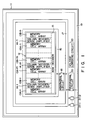
- a memory area 12 is disposed in the central portion of a chip 11 (semiconductor body).
- Memory cell arrays 13A-1, 13B-1, ---, 13A-m, 13B-m, ---, 13A-n, 13B-n, column decoders/sense amplifiers 14-1, ---14-m, ---, 14-n, and a row decoder 15 are arranged in the memory area 12.
- Memory cells are arranged in a matrix form in the respective memory cell arrays 13A-1, 13B-1, ---, 13A-m, 13B-m, ---, 13A-n, 13B-n.
- the column decoder selects the columns of the memory cell arrays 13A-1, 13B-1, ---, 13A-m, 13B-m, ---, 13A-n, 13B-n.
- the row decoder 15 selects the rows of the memory cell arrays 13A-1, 13B-1, ---, 13A-m, 13B-m, ---, 13A-n, 13B-n.
- the sense amplifier amplifies and outputs data read out from a memory cell selected by the column decoder and the row decoder 15.
- the power source line 16 applies the potential Vint to the sense amplifier, column decoder, row decoder and the like in the memory area 12 as a power source potential.
- a second power source line 17 applied with a ground potential Vss is disposed in the surrounding region of the power source line 16.
- a first peripheral circuit 18 driven by a potential difference between the power source lines 16 and 17 is provided in that area of the chip 11 which lies between the power source lines 16 and 17.
- the first peripheral circuit 18 is a circuit used for the memory area 12, for example, an address buffer circuit.
- a third power source line 19 applied with a power source potential Vext of 5V, for example, from the exterior of the chip 11 is disposed in the surrounding region of the power source line 17.
- a second peripheral circuit 20 driven by a potential difference between the power source lines 19 and 17, data output or input pads 21-1 to 21-p and a voltage lowering circuit 22 are provided in that area of the chip 11 which lies between the power source lines 19 and 17.
- the peripheral circuit 20 is a circuit used for the external portion of the chip 11, for example, an input/output buffer and an input protection circuit.
- the pads 21-1 to 21-p are provided only for the partial area in Fig. 1, but in practice, they are formed at a regular interval in the area between the power source lines 19 and 17 to surround the memory area 12.
- the voltage lowering circuit 22 creates the potential Vint by lowering the potential difference (5V) between the potential Vext applied to the power source line 19 and the potential Vss applied to the power source line 17 to a certain potential level (3.0 to 3.5V) and applies the thus created potential to the power source line 16.
- the voltage lowering circuit 22 is not necessary.
- a semiconductor memory device in which the power source lines 16, 17 and 19 and the first and second peripheral circuits 18 and 20 can be efficiently arranged on the chip 11 and an increase in the chip area caused by use of the three power source lines 16, 17 and 19 can be suppressed to a minimum.
- the peripheral circuit 18 can be efficiently arranged and the high degree of integration can be attained irrespective of the presence of the second peripheral circuit 20 even if the area for the first peripheral circuit 18 is increased with an increase in the memory capacity (4 M-bit, 16 M-bit, 64 M-bit, 256 M-bit, ---).
- the power source line 19 is disposed near the outer end portion of the chip 11, and the second peripheral circuit 20, pads 21-1 to 21-p and voltage lowering circuit 22 are arranged in the area between the power source lines 19 and 17, the degree of freedom of the pattern design can be enhanced.
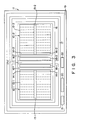
- Fig. 2 is a pattern plan view schematically showing the chip layout of a semiconductor memory device according to a second embodiment of this invention.
- a single memory area is formed in the central portion of the chip 11, but in the second embodiment, this invention is applied to a case wherein a plurality of memory areas (two in this embodiment) are provided, that is, the memory area in the pattern shown in Fig. 1 is divided into a plurality of portions (two portions).
- First and second memory areas 12-1 and 12-2 are separately disposed in the central portion of the chip 11. Like the case of Fig. 1, memory cell arrays 13-1 and 13-2, column decoders/sense amplifiers 14-1 and 14-2, and row decoders 15-1 and 15-2 are formed in the respective memory areas 12-1 and 12-2.
- a first power source line 16 applied with a potential Vint is formed around the memory areas 12-1 and 12-2.
- a portion 16X of the power source line 16 is formed to pass through substantially the central portion of an area between the memory areas 12-1 and 12-2.
- a second power source line 17 is formed to surround the first power source line 16. The power source line 17 is applied with a ground potential Vss.
- Portions 17Y and 17Z of the power source line 17 are formed on both sides of the portion 16X on an area between the memory areas 12-1 and 12-2.
- a peripheral circuit 18-1 driven by a voltage between the power source line portions 16X and 17Y is formed in an area defined by the portions 16X and 17Y of the power source lines and lying between the memory areas 12-1 and 12-2 and a peripheral circuit 18-2 driven by a voltage between the power source line portions 16X and 17Z is formed in an area defined by the portions 16X and 17Z of the power source lines.
- a third power source line 19 is formed in the surrounding region of the second power source line 17 along the outer periphery of the chip 11. The power source line 19 is applied with a potential Vext given from the exterior of the chip 11.
- a second peripheral circuit 20, pad 21 and voltage lowering circuit 22 are formed in an area between the power source lines 17 and 19.
- the voltage lowering circuit 22 lowers the potential Vext (5V) supplied to the power source line 19 from the exterior to a level (3.0 to 3.5V) and applies the lowered potential to the peripheral circuits 18-1 and 18-2 and the memory areas 12-1 and 12-2 via the first power source line 16.
- the patterns of the first and second power source lines 16 and 17 may be formed to overlap on each other as shown in Fig. 2 by using a first-level layer containing aluminum as the second power source line 17, using a second-level layer containing aluminum as the first power source line 16, and forming an insulation film between the first- and second level layers. Further, the first-level layer, second-level layer or a layer containing aluminum and formed above the first- and second-level layers may be used as the third power source line 19.
- the power source line 16 can be commonly used by the peripheral circuit 18-1 used for the memory area 12-1 and the peripheral circuit 18-2 used for the memory area 12-2 in the area between the two memory areas 12-1 and 12-2.
- the three types of power source lines 16, 17 and 19, the peripheral circuits 18-1, 18-2 and 20 driven by potential differences between the power source lines 16, 17 and 19 and the voltage lowering circuit 22 can be efficiently arranged on the chip 11.
- Fig. 3 is a pattern plan view schematically showing the chip layout of a semiconductor memory device according to a third embodiment of this invention.
- the portion 16X of the first power source line 16 is formed in the area between the memory areas 12-1 and 12-2 and the portions 17Y and 17Z of the second power source line 17 are disposed on both sides of the power source line 16, but in the third embodiment, a portion 17X of a second power source line 17 is formed in the central area of an area between the memory areas 12-1 and 12-2 and portions 16Y and 16Z of a first power source line 16 are formed on both sides of the second power source line.
- portions which are the same as those of Fig. 2 are denoted by the same reference numerals and the detail explanation therefor is omitted.
- a semiconductor memory device can be provided in which three power source lines applied with three different potentials, a first peripheral circuit driven by a power source potential supplied from the exterior and a peripheral circuit driven by a lowered power source potential can be efficiently arranged on a chip even when the power source voltage for the memory area and the peripheral circuit used for the memory area is lowered in order to suppress reduction in the breakdown voltage of the miniaturized memory cell and ensure the high reliability.
Landscapes
- Engineering & Computer Science (AREA)
- Power Engineering (AREA)
- Dram (AREA)
- Semiconductor Integrated Circuits (AREA)
- Semiconductor Memories (AREA)
Claims (19)
- Halbleiterspeichervorrichtung, in welcher ein an ein Speichergebiet angelegtes Energieversorgungspotential erniedrigt wird auf einen Pegel, welcher niedriger ist als ein von außen zugeführtesEnergieversorgungspotential, umfassend einen Halbleiterkörper (11); ein Speichergebiet (12), welches in dem Halbleiterkörper (11) vorgesehen ist;gekennzeichnet durch eine erste Energieversorgungsleitung (16), welche um das Speichergebiet (12) angeordnet ist, und an welcher ein erstes Potential anliegt; eine zweite Energieversorgungsleitung (17), welche in dem Umgebungsbereich der ersten Energieversorgungsleitung (16) angeordnet ist, und an welcher ein zweites Potential anliegt; eine erste Schaltung (18), welche in jenem Gebiet des Halbleiterkörpers (11) angeordnet ist, welches zwischen den ersten und zweiten Energieversorgungsleitungen (16 und 17) liegt, undwelche von einer Potentialdifferenz zwischen den ersten und zweiten Potentialen angetrieben wird; eine dritte Energieversorgungsleitung (19), angeordnet in dem Umgebungsbereich der zweiten Energieversorgungsleitung (17) und an welcher ein drittes Potential anliegt; undeine zweite Schaltung (20), welche in jenem Gebiet des Halbleiterkörpers (11) angeordnet ist, welches zwischen den ersten und dritten Energieversorgungsschaltungen (17 und 19) liegt, und welche von einer Potentialdifferenz zwischen den zweiten und dritten Potentialen angetrieben wird.
- Vorrichtung nach Anspruch 1,dadurch gekennzeichnet, daßsie ferner eine Spannungserniedrigungsvorrichtung (22) umfaßt, zur Schaffung des ersten Potentials durch Erniedrigung des dritten Potentials und zum Anlegen des ersten Potentials an die erste Energieversorgungsleitung (16).
- Vorrichtung nach Anspruch 2,dadurch gekennzeichnet, daßdie Spannungserniedrigungsvorrichtung (22) in jenem Gebiet des Halbleiterkörpers (11) vorgesehen ist, welches zwischen den zweiten und dritten Energieversorgungsleitungen (17 und 19) liegt.
- Vorrichtung nach Anspruch 1,dadurch gekennzeichnet, daßdas Speichergebiet (12) ein Speicherzellarray (13A-1, 13B-1, ---, 13A-m, 13B-m, ---, 13A-n, 13B-n), enthält, einen Zeilendecoder (15) zur Auswahl einer Zeile in dem Speicherzellarray (13A-1, 13B-1, ---, 13A-m, 13B-m, ---, 13A-n, 13B-n), einen Spaltendecoder zur Auswahl einer Spalte des Speicherzellarrays, und einen Leseverstärker zur Verstärkung von Daten, welche aus einer von dem Zahlendecoder (15) und dem Spaltendecoder ausgewählten Speicherzelle ausgelesen werden.
- Vorrichtung nach Anspruch 1,dadurch gekennzeichnet, daßdas dritte Potential ein Energieversorgungspotential (Vext) ist, welches von außen zugeführt wird, das zweite Potential ein Erdpotential (Vss) ist, welches von außen zugeführt wird, und das erste Potential ein Potential (Vint) ist, welches zwischen dem Energieversorgungspotential und dem Erdpotential ist.
- Vorrichtung nach Anspruch 1,dadurch gekennzeichnet, daßdie erste Schaltung (18) eine Schaltung enthält zur Übertragung von Daten bezüglich dem Speichergebiet (12).
- Vorrichtung nach Anspruch 1,dadurch gekennzeichnet, daßdie Schaltung zur Übertragung von Daten bezüglich dem Speichergebiet (12) einen Adreßpuffer enthält.
- Vorrichtung nach Anspruch 1,dadurch gekennzeichnet, daßdie zweite Schaltung (20) eine Schaltung zur Übertragung von Daten nach/von außen enthält.
- Vorrichtung nach Anspruch 8,dadurch gekennzeichnet, daßdie Schaltung zur Übertragung von Daten nach/von außen einen Eingabe/Ausgabe-Puffer enthält.
- Halbleiterspeichervorrichtung, in welcher ein an ein Speichergebiet angelegtes Energieversorgungspotential auf einen Pegel erniedrigt ist, welcher niedriger ist als ein von außen zugeführtes Energieversorgungspotential, umfassend einen Halbleiterkörper (11); gekennzeichnet durch ein erstes Speichergebiet (12-1), welches in dem Halbleiterkörper (11) vorgesehen ist; ein zweites Halbleitergebiet (12-2), welches in dem Halbleiterkörper (11) an einem von dem ersten Speichergebiet (12-1) getrennten Ort vorgesehen ist; eine erste Energieversorgungsleitung (16), welche einen Abschnitt umfaßt, der die ersten und zweiten Speichergebiete (12-1 und 12-2) umgibt und mindestens einen weiteren Abschnitt (16X oder 16Y, 16Z), welcher sich zwischen den ersten und zweiten Speichergebieten (12-1 und 12-2) befindet, und an welcher ein erstes Potential anliegt; eine zweite Energieversorgungsleitung (17), welche einen Abschnitt umfaßt, der die erste Energieversorgungsleitung (16) umgibt, und mindestens einen weiteren Abschnitt (17Y, 17Z oder 17X), welcher sich zwischen den ersten und zweiten Speichergebieten (12-1 und 12-2) befindet, und an welcher ein zweites Potential anliegt, wobei die zweite Energieversorgungsleitung (17) aus einer Schicht gebildet ist, welche sich in einem Niveau befindet, welches verschieden ist von dem einer Schicht, die die erste Energieversorgungsleitung (16) bildet;eine erste Schaltung (18-1, 18-2), welche in dem Gebiet des Halbleiterkörpers (11) angeordnet ist, welche zwischen dem zumindest weiteren Abschnitt (16X oder 16Y, 16Z) der ersten Energieversorgungsleitung (16) und dem zumindest weiteren Abschnitt (17Y, 17Z oder 17X) der zweiten Energieversorgungsleitung (17) liegt, und welche angetrieben wird von einer Potentialdifferenz zwischen dem ersten und beiden Potentialen; eine dritte Energieversorgungsleitung (19), welche in dem Umgebungsgebiet der zweiten Energieversorgungsleitung (17) angeordnet ist und an welcher ein drittes Potential anliegt; und eine zweite Schaltung (20), welche in dem Gebiet des Halbleiterkörpers (11) angeordnet ist, welches zwischen dem zweiten und dritten Energieversorgungsleitungen (17 und 19) liegt, und welches angetrieben wird von einer Potentialdifferenz zwischen den zweiten und dritten Potentialen.
- Vorrichtung nach Anspruch 10,dadurch gekennzeichnet, daßdie Spannungserniedrigungsvorrichtung (22) in jenem Gebiet des Halbleiterkörpers (11) vorgesehen ist, welches zwischen den zweiten und dritten Energieversorgungsleitungen (17 und 19) liegt.
- Vorrichtung nach Anspruch 11,dadurch gekennzeichnet, daßdie Spannungserniedrigungsvorrichtung (22) in jenem Gebiet des Halbleiterkörpers (11) vorgesehen ist, welches zwischen den zweiten und dritten Energieversorgungsleitungen (17 und 19) liegt.
- Vorrichtung nach Anspruch 10,dadurch gekennzeichnet, daßjedes der ersten und zweiten Speichergebiete (12-1 und 12-2) Speicherzellarrays (13-1, 13-2) enthält, einen Zeilendecoder (15-1, 15-2), zur Auswahl von Zeilen der Speicherzellarrays (13-1, 13-2), einen Spaltendecoder zur Auswahl von Spalten der Speicherzellarrays (13-1, 13-2), und einen Leseverstärker zur Verstärkung von Daten, welche aus von dem Zeilendecoder (15-1, 15-2) und dem Spaltendecoder ausgewählten Zellen ausgelesen werden.
- Vorrichtung nach Anspruch 10,dadurch gekennzeichnet, daßdie zweite Energieversorgungsleitung (17) aus einer ersten Schicht eines ersten Niveaus, welches Aluminium enthält, gebildet ist, und die erste Energieversorgungsleitung (16) aus einer zweiten Schicht eines zweiten Niveaus, welches Aluminium enthält, gebildet ist.
- Vorrichtung nach Anspruch 10,dadurch gekennzeichnet, daßdas dritte Potential ein von außen zugeführtes Energieversorgungspotential (Vext) ist, das zweite Potential ein von außen zugeführtes Erdpotential (Vss) ist, und das erste Potential ein Potential (Vint) zwischen dem Energieversorgungspotential und dem Erdpotential ist.
- Vorrichtung nach Anspruch 10,dadurch gekennzeichnet, daßdie erste Schaltung (18-1, 18-2) eine Schaltung enthält zur Übertragung von Daten bezüglich dem Speichergebiet (12-1, 12-2).
- Vorrichtung nach Anspruch 10,dadurch gekennzeichnet, daßdie Vorrichtung zur Übertragung von Daten bezüglich dem Speichergebiet (12-1, 12-2) einen Adreßpuffer enthält.
- Vorrichtung nach Anspruch 10,dadurch gekennzeichnet, daßdie zweite Schaltung (20) eine Schaltung enthält zur Übertragung von Daten von/nach außen.
- Vorrichtung nach Anspruch 18,dadurch gekennzeichnet, daßdie Schaltung zur Übertragung von Daten von/nach außen einen Eingabe/Ausgabe-Puffer enthält.
Applications Claiming Priority (2)
| Application Number | Priority Date | Filing Date | Title |
|---|---|---|---|
| JP2329856A JP2894635B2 (ja) | 1990-11-30 | 1990-11-30 | 半導体記憶装置 |
| JP329856/90 | 1990-11-30 |
Publications (3)
| Publication Number | Publication Date |
|---|---|
| EP0488303A2 EP0488303A2 (de) | 1992-06-03 |
| EP0488303A3 EP0488303A3 (en) | 1993-01-27 |
| EP0488303B1 true EP0488303B1 (de) | 1996-07-17 |
Family
ID=18226002
Family Applications (1)
| Application Number | Title | Priority Date | Filing Date |
|---|---|---|---|
| EP91120419A Expired - Lifetime EP0488303B1 (de) | 1990-11-30 | 1991-11-28 | Speisespannungsleitungsanordnung in einer Halbleiterspeicheranordnung |
Country Status (5)
| Country | Link |
|---|---|
| US (1) | US5293334A (de) |
| EP (1) | EP0488303B1 (de) |
| JP (1) | JP2894635B2 (de) |
| KR (1) | KR960000714B1 (de) |
| DE (1) | DE69120906T2 (de) |
Families Citing this family (12)
| Publication number | Priority date | Publication date | Assignee | Title |
|---|---|---|---|---|
| KR0137105B1 (ko) * | 1993-06-17 | 1998-04-29 | 모리시다 요이치 | 데이터 전송회로, 데이터선 구동회로, 증폭회로, 반도체 집적회로 및 반도체 기억장치 |
| KR970005691B1 (ko) * | 1993-09-06 | 1997-04-18 | 삼성전자주식회사 | 전원노이즈감소를 위한 전원라인구조를 가지는 반도체칩 |
| US6009034A (en) * | 1995-08-15 | 1999-12-28 | Micron Technology, Inc. | Memory device with distributed voltage regulation system |
| US5574697A (en) * | 1995-08-15 | 1996-11-12 | Micron Technology, Inc. | Memory device with distributed voltage regulation system |
| JP3581459B2 (ja) * | 1995-10-24 | 2004-10-27 | 株式会社ルネサステクノロジ | 半導体記憶装置 |
| JP3556388B2 (ja) * | 1996-04-23 | 2004-08-18 | 株式会社 沖マイクロデザイン | 半導体メモリ装置 |
| US5748549A (en) * | 1996-05-27 | 1998-05-05 | Mitsubishi Denki Kabushiki Kaisha | Semiconductor memory device |
| US5936877A (en) * | 1998-02-13 | 1999-08-10 | Micron Technology, Inc. | Die architecture accommodating high-speed semiconductor devices |
| JP4963144B2 (ja) * | 2000-06-22 | 2012-06-27 | ルネサスエレクトロニクス株式会社 | 半導体集積回路 |
| US20060077002A1 (en) * | 2004-10-08 | 2006-04-13 | White Richard T | Apparatus and methods for saving power and reducing noise in integrated circuits |
| JP2016092536A (ja) | 2014-10-31 | 2016-05-23 | ルネサスエレクトロニクス株式会社 | 半導体装置 |
| KR102749326B1 (ko) * | 2018-08-21 | 2025-01-03 | 엘에스엠트론 주식회사 | 자동화변속기의 유압클러치 보정 방법 |
Family Cites Families (17)
| Publication number | Priority date | Publication date | Assignee | Title |
|---|---|---|---|---|
| CH421861A (it) * | 1964-06-10 | 1966-09-30 | Monacelli Umberto | Macchina pneumatica per il fissaggio di punti metallici |
| JPS5840344B2 (ja) * | 1980-06-10 | 1983-09-05 | 富士通株式会社 | 半導体記憶装置 |
| JPS57124463A (en) * | 1981-01-26 | 1982-08-03 | Nec Corp | Semiconductor device |
| JPS58114392A (ja) * | 1981-12-07 | 1983-07-07 | Fujitsu Ltd | 半導体記憶装置 |
| JPS59135747A (ja) * | 1983-01-24 | 1984-08-04 | Mitsubishi Electric Corp | 大規模集積回路装置 |
| US4695978A (en) * | 1984-11-15 | 1987-09-22 | Fujitsu Limited | Semiconductor memory device |
| JPH0738583B2 (ja) * | 1985-01-26 | 1995-04-26 | 株式会社東芝 | 半導体集積回路 |
| JPH0789568B2 (ja) * | 1986-06-19 | 1995-09-27 | 日本電気株式会社 | 集積回路装置 |
| JPS6326893A (ja) * | 1986-07-18 | 1988-02-04 | Mitsubishi Electric Corp | 半導体メモリ装置 |
| JPS6394499A (ja) * | 1986-10-07 | 1988-04-25 | Toshiba Corp | 半導体記憶装置 |
| US4884115A (en) * | 1987-02-27 | 1989-11-28 | Siemens Aktiengesellschaft | Basic cell for a gate array arrangement in CMOS Technology |
| JPS6415948A (en) * | 1987-07-09 | 1989-01-19 | Nec Corp | Semiconductor integtated circuit |
| JPS6435934A (en) * | 1987-07-30 | 1989-02-07 | Hitachi Ltd | Semiconductor integrated circuit device |
| KR910008099B1 (ko) * | 1988-07-21 | 1991-10-07 | 삼성반도체통신주식회사 | 메모리 칩의 파워 및 시그널라인 버싱방법 |
| JPH0744223B2 (ja) * | 1988-08-17 | 1995-05-15 | 株式会社東芝 | 電源配線構造の設計方法 |
| JPH0268439A (ja) * | 1988-09-02 | 1990-03-07 | Daikin Ind Ltd | 空気調和機の制御装置 |
| JP2906148B2 (ja) * | 1988-11-01 | 1999-06-14 | 松下電器産業株式会社 | 半導体集積回路 |
-
1990
- 1990-11-30 JP JP2329856A patent/JP2894635B2/ja not_active Expired - Fee Related
-
1991
- 1991-11-27 US US07/799,078 patent/US5293334A/en not_active Expired - Lifetime
- 1991-11-28 DE DE69120906T patent/DE69120906T2/de not_active Expired - Fee Related
- 1991-11-28 EP EP91120419A patent/EP0488303B1/de not_active Expired - Lifetime
- 1991-11-29 KR KR1019910021789A patent/KR960000714B1/ko not_active Expired - Fee Related
Also Published As
| Publication number | Publication date |
|---|---|
| EP0488303A3 (en) | 1993-01-27 |
| KR920010906A (ko) | 1992-06-27 |
| US5293334A (en) | 1994-03-08 |
| KR960000714B1 (ko) | 1996-01-11 |
| DE69120906T2 (de) | 1996-12-19 |
| JPH04206659A (ja) | 1992-07-28 |
| DE69120906D1 (de) | 1996-08-22 |
| EP0488303A2 (de) | 1992-06-03 |
| JP2894635B2 (ja) | 1999-05-24 |
Similar Documents
| Publication | Publication Date | Title |
|---|---|---|
| JP4534132B2 (ja) | 積層型半導体メモリ装置 | |
| KR100268961B1 (ko) | 반도체 장치 및 그 제조 방법과 메모리 코어 칩 및 메모리 주변 회로 칩 | |
| EP0130798B1 (de) | Halbleiterspeicheranordnung | |
| US7638871B2 (en) | Semiconductor device | |
| US6094382A (en) | Integrated circuit memory devices with improved layout of fuse boxes and buses | |
| EP0488303A2 (de) | Speisespannungsleitungsanordnung in einer Halbleiterspeicheranordnung | |
| JP3374967B2 (ja) | 半導体集積回路 | |
| KR0172426B1 (ko) | 반도체 메모리장치 | |
| US6069812A (en) | Integrated circuit memory devices including rows of pads extending parallel to the short sides of the integrated circuit | |
| JPS6240760A (ja) | 半導体記憶装置 | |
| JP3154650B2 (ja) | 半導体装置 | |
| US5184321A (en) | Semiconductor memory device comprising a plurality of memory arrays with improved peripheral circuit location and interconnection arrangement | |
| US5101377A (en) | Semiconductor memory device | |
| JP4574784B2 (ja) | 半導体装置および半導体装置のレイアウト方法 | |
| KR100401320B1 (ko) | 반도체 장치 | |
| US5930166A (en) | Semiconductor memory device with triple metal layer | |
| US6104627A (en) | Semiconductor memory device | |
| JP3048963B2 (ja) | 半導体メモリ装置 | |
| KR890002888A (ko) | 반도체 집적회로장치 | |
| CN114373745B (zh) | 半导体装置中的esd放置 | |
| EP0541360B1 (de) | Halbleiterspeicheranordnung | |
| JPH03225697A (ja) | 半導体集積回路 | |
| JPS60175438A (ja) | 半導体集積回路装置 | |
| JPH0358544B2 (de) | ||
| CN120237118A (zh) | 一种三维存储器和电子设备 |
Legal Events
| Date | Code | Title | Description |
|---|---|---|---|
| PUAI | Public reference made under article 153(3) epc to a published international application that has entered the european phase |
Free format text: ORIGINAL CODE: 0009012 |
|
| 17P | Request for examination filed |
Effective date: 19911128 |
|
| AK | Designated contracting states |
Kind code of ref document: A2 Designated state(s): DE FR GB |
|
| PUAL | Search report despatched |
Free format text: ORIGINAL CODE: 0009013 |
|
| AK | Designated contracting states |
Kind code of ref document: A3 Designated state(s): DE FR GB |
|
| 17Q | First examination report despatched |
Effective date: 19951011 |
|
| GRAH | Despatch of communication of intention to grant a patent |
Free format text: ORIGINAL CODE: EPIDOS IGRA |
|
| GRAA | (expected) grant |
Free format text: ORIGINAL CODE: 0009210 |
|
| AK | Designated contracting states |
Kind code of ref document: B1 Designated state(s): DE FR GB |
|
| GRAH | Despatch of communication of intention to grant a patent |
Free format text: ORIGINAL CODE: EPIDOS IGRA |
|
| REF | Corresponds to: |
Ref document number: 69120906 Country of ref document: DE Date of ref document: 19960822 |
|
| ET | Fr: translation filed | ||
| PLBE | No opposition filed within time limit |
Free format text: ORIGINAL CODE: 0009261 |
|
| STAA | Information on the status of an ep patent application or granted ep patent |
Free format text: STATUS: NO OPPOSITION FILED WITHIN TIME LIMIT |
|
| 26N | No opposition filed | ||
| REG | Reference to a national code |
Ref country code: GB Ref legal event code: IF02 |
|
| PGFP | Annual fee paid to national office [announced via postgrant information from national office to epo] |
Ref country code: DE Payment date: 20081120 Year of fee payment: 18 |
|
| PGFP | Annual fee paid to national office [announced via postgrant information from national office to epo] |
Ref country code: FR Payment date: 20081112 Year of fee payment: 18 |
|
| PGFP | Annual fee paid to national office [announced via postgrant information from national office to epo] |
Ref country code: GB Payment date: 20081126 Year of fee payment: 18 |
|
| GBPC | Gb: european patent ceased through non-payment of renewal fee |
Effective date: 20091128 |
|
| REG | Reference to a national code |
Ref country code: FR Ref legal event code: ST Effective date: 20100730 |
|
| PG25 | Lapsed in a contracting state [announced via postgrant information from national office to epo] |
Ref country code: FR Free format text: LAPSE BECAUSE OF NON-PAYMENT OF DUE FEES Effective date: 20091130 |
|
| PG25 | Lapsed in a contracting state [announced via postgrant information from national office to epo] |
Ref country code: DE Free format text: LAPSE BECAUSE OF NON-PAYMENT OF DUE FEES Effective date: 20100601 |
|
| PG25 | Lapsed in a contracting state [announced via postgrant information from national office to epo] |
Ref country code: GB Free format text: LAPSE BECAUSE OF NON-PAYMENT OF DUE FEES Effective date: 20091128 |