EP0475709B1 - Zur Unterdrückung der Gleichstrommagnetisierung im Drehstromtransformator Wechselrichtersteuersatz - Google Patents
Zur Unterdrückung der Gleichstrommagnetisierung im Drehstromtransformator Wechselrichtersteuersatz Download PDFInfo
- Publication number
- EP0475709B1 EP0475709B1 EP91308223A EP91308223A EP0475709B1 EP 0475709 B1 EP0475709 B1 EP 0475709B1 EP 91308223 A EP91308223 A EP 91308223A EP 91308223 A EP91308223 A EP 91308223A EP 0475709 B1 EP0475709 B1 EP 0475709B1
- Authority
- EP
- European Patent Office
- Prior art keywords
- output
- current
- phase
- inverter
- control device
- Prior art date
- Legal status (The legal status is an assumption and is not a legal conclusion. Google has not performed a legal analysis and makes no representation as to the accuracy of the status listed.)
- Expired - Lifetime
Links
Images

Classifications
-
- H—ELECTRICITY
- H02—GENERATION; CONVERSION OR DISTRIBUTION OF ELECTRIC POWER
- H02M—APPARATUS FOR CONVERSION BETWEEN AC AND AC, BETWEEN AC AND DC, OR BETWEEN DC AND DC, AND FOR USE WITH MAINS OR SIMILAR POWER SUPPLY SYSTEMS; CONVERSION OF DC OR AC INPUT POWER INTO SURGE OUTPUT POWER; CONTROL OR REGULATION THEREOF
- H02M7/00—Conversion of ac power input into dc power output; Conversion of dc power input into ac power output
- H02M7/42—Conversion of dc power input into ac power output without possibility of reversal
- H02M7/44—Conversion of dc power input into ac power output without possibility of reversal by static converters
- H02M7/48—Conversion of dc power input into ac power output without possibility of reversal by static converters using discharge tubes with control electrode or semiconductor devices with control electrode
- H02M7/4803—Conversion of dc power input into ac power output without possibility of reversal by static converters using discharge tubes with control electrode or semiconductor devices with control electrode with means for reducing DC component from AC output voltage
Definitions
- This invention relates to a control device that controls a self-commutated inverter connected to an AC (alternating-current) power system via a three-phase transformer, and more particularly to an inverter control device that suppresses DC (direct-current) magnetization generated in three-phase transformer.
- a typical voltage self-commutated inverter is composed of an inverter main circuit, which contains a plurality of controllable rectifier elements and a plurality of rectifier elements, a DC capacitor connected across a DC side terminals of the inverter main circuit, and a three-phase transformer having the inverter side terminals connected to a AC side terminals of the inverter main circuit on a phase basis and the system terminals connected to the system on a phase basis.
- Such an inverter is able to control the three phase output voltages of the inverter main circuit by changing ON time of the individual controllable rectifier elements.
- the current exchanged with the AC power system via the impedance of the three-phase transformer can be controlled by regulating the phase and amplitude of the three phase output voltages from the inverter main circuit according to the phase and amplitude of the AC system voltage.
- Such inverter control is performed by an inverter control device. Based on the active current reference value and reactive current reference value, the inverter control device determines an inverter output voltage reference value that decides the three phase output voltages of the inverter main circuit and then supplies a gate signal corresponding to the inverter output voltage reference value to the inverter main circuit to control the ON time of each controllable rectifier element. This converts the DC powerfrom the DC voltage source connected to the DC side terminals of the inverter main circuit into an effective power and supplies it to the AC power system or regulates the reactive power of the AC power system.
- the above-mentioned inverter control device has the following problem: a constant generation of a small amount of DC component in the three phase output AC voltages of the inverter main circuit creates a DC component in the alternating magnetic flux in the three-phase transformer, causing an excessive exciting current to flow. That is, DC magnetization in the three-phase transformergives rise to overcurrent.
- the transformer When DC magnetization in the three-phase transformer permits a current larger than the rated value to flow in the windings of the three-phase transformer, the transformer may burn out and an excessive current may flow through the controllable rectifier elements constituting the inverter main circuit, which destroys the elements, preventing the voltage self-commutated inverter from functioning properly.
- the reason why a small amount of DC component is produced in the three phase output AC voltages of the inverter main circuit is that slight differences in characteristic between the controllable rectifier elements making up the inverter main circuit lead to differences in ON time between the controllable rectifier elements on the positive and negative polarity sides, creating a DC component in the output voltage.
- the generation of a DC component in the inverter output voltage reference value also causes DC components in the three phase output AC voltages of the inverter main circuit.
- EP-A3-0220638 discloses deleting a DC magnetic polarization amount from the AC output supplied to a load in a single phase constant voltage constant frequency power supply.
- the object of the present invention is to provide a highly reliable inverter control device capable of preventing not only the generation of overcurrent due to DC magnetization in the three-phase transformer, but also burnouts of the three-phase transformer and controllable rectifier elements.
- an inverter control device comprising: an inverter control device according to this invention, comprising: a current DC component detecting circuit for detecting the current DC components contained in at least two of the three phase output AC currents of the inverter; a DC magnetization suppressor signal generating circuit for producing two correcting signals from the current DC components, the two correcting signals being used to balance in amount the three voltage DC components contained in the three phase output AC voltages of the inverter respectively; an output reference correcting circuit for correcting two of first output references in accordance with the two correcting signals and outputting three second references including the two corrected values and one of the first output reference; and a gate control circuit for controlling the three phase output AC voltages of the inverter according to the three second output references.
- the voltage DC components for two phases are regulated so that the imbalanced components contained in the three phase output AC voltages of the inverter may become zero between phases, which causes the DC current component of each phase to be zero, thereby suppressing DC magnetization.
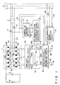
- Fig. 1 shows an overall arrangement of an embodiment of the present invention.
- a DC capacitor 2 is connected across the DC side terminals of an inverter main circuit 1, the AC side terminals of which are connected to a three-phase transformer 3 on a phase basis: R phase, S phase, and T phase.
- Those inverter main circuit 1, DC capacitor 2, and three-phase transformer 3 constitute a voltage self-commutated inverter.
- This inverter is connected to a DC voltage source 4 via the DC side terminals of the inverter main circuit 1, while connected to a three-phase power system 5 via the three-phase transformer 3.
- the inverter main circuit 1 is constructed by connecting controllable rectifier elements GU, GV, GW, GX, GY, and GZ, and rectifier elements DU, DV, DW, DX, DY, and DZ as shown in Fig. 1.
- controllable rectifier elements GU, GV, GW, GX, GY, and GZ power electronics elements with a self-extinguishing function, such as GTOs (Gate Turn Off transistors) or power transistors may be used.
- An inverter control device is composed of Hall CT circuits 11 and 12, which detect the R-phase and T-phase inverter output AC currents, respectively, a current DC component detector 13, a DC magnetization suppressor signal generating circuit 14, a synchronous phase detecting circuit 15, which detects the system voltage phase 0 of the system voltages VR, VS, and VT of the three-phase AC system 5, an active current setting unit 16 to enter the active current reference value, a reactive current setting unit 17 to enter the reactive current reference value, an inverter output-voltage reference generating circuit 18, an output reference correcting circuit 19, and PWM gate controlling circuit 20.
- the Hall CT circuits 11 and 12 are installed on the R-phase and T-phase lines L1 and L3 among the conductor wires L1 through L3 that connect the AC side terminals of the inverter main circuit 1 with the inverter side terminals of the three-phase transformer 3 on a phase basis.
- the Hall CT circuit 11 detects a Hall voltage, which is generated when the magnetic flux, caused by the current flowing through the line L1, penetrates through the Hall element, and supplies the output as an electrical signal.
- the Hall CT circuit 12 functions the same way.
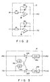
- the current DC component detector 13 is constructed as shown in Fig. 2, where reference charac- terA indicates an operational amplifier, R1 and R2 indicate resistors, and C indicates a capacitor. Here, two operational amplifier A, resistors R1 and R2, and capacitors C make up two first-order time-lag circuits.
- the current DC component detector 13 detects DC components iRd and iTd from the inverter output AC currents iR and iT supplied from the Hall CT circuits 11 and 12.
- the DC magnetization suppressor signal generating circuit 14 Based on the DC components iRd and iTd from the current DC component detector 13, the DC magnetization suppressor signal generating circuit 14, which is constructed as shown in Fig. 3, obtains the inverter output voltage correcting signals VRd and VTd that balance the DC components in the three phase inverter output AC currents, and supplies the signal VRd and VTd.
- the inverter output voltage reference generating circuit 18 receives the inverter output AC currents iR and iT, system voltage phase 0, active current reference value idc, and reactive current reference value iqc.
- the output reference correcting circuit 19 which is composed of two adders 31 and 32 as shown in Fig. 1, receives the inverter output voltage references VRC, VSC, and VTC and the inverter output voltage correcting signals VRd and VTd.
- the correcting circuit 19 corrects the inverter output voltage references VRC and VTC on a phase basis, according to the inverter output voltage correcting signals VRd and VTd, and supplies the corrected inverter output voltage references VRCC and VTCC as the two of second output references.
- the inverter output voltage reference VSC is supplied as the corrected output reference VSCC as the one of the second output reference without correction. The reason for this will be explained later.
- the PWM gate control circuit 20 compares the corrected output references VRCC, VSCC, and VTCC with a triangular wave carrier signal and supplies gate signals that determine the ON time of each of the controllable rectifier elements GU, GV, GW, GX, GY, and GZ constituting the inverter main circuit 1.
- Fig. 4 shows a circuit for explaining a DC magnetization phenomenon in the transformer during inverter operation
- Fig. 5 is a circuit for depicting the principle of suppressing DC magnetization in the three-phase transformer.
- Fig. 4 For shortness' sake, DC magnetization will be described, referring to Fig. 4. It is known that single- phase transformers have an equivalent circuit as shown in Fig. 4, where reference character Z1 indicates the leakage impedance (the winding resistance plus the leakage inductance) on the inverter main circuit side of the transformer, Z2 indicates the leakage impedance on the AC system side of the transformer, and Zm indicates the magnetizing impedance (the iron loss plus the magnetizing inductance) of the transformer.
- Z1 indicates the leakage impedance (the winding resistance plus the leakage inductance) on the inverter main circuit side of the transformer
- Z2 indicates the leakage impedance on the AC system side of the transformer
- Zm indicates the magnetizing impedance (the iron loss plus the magnetizing inductance) of the transformer.
- the inverter main circuit, transformer, and AC system will form a circuit of Fig. 4 with respect to the DC voltage component E.
- DC currents i1 and i2 will flow.
- DC current flowing through the magnetizing inductance of the transformer causes DC magnetization. That is, the DC current i1 causes DC magnetization. Since the magnetizing inductance is much larger than the leakage impedance, it will take long time for the DC current i1 to become so large that the magnetic flux in the transformer is saturated to generated an AC overcurrent.
- impedances ZmR, ZmS, and ZmT the impedances corresponding to the inductances of the transformer and AC system are combined into a single impedance for each phase: impedances ZmR, ZmS, and ZmT.
- equations (4) and (5) are calculated at the DC magnetization suppressor signal generating circuit 14 constructed as shown in Fig. 3.
- Reference character 21a and 21 b indicate amplifiers that multiply by a constant of 1/2 in equations (4) and (5), 22a and 22b adders that calculate the terms in braces in equations (4) and (5), and 23a and 23b amplifiers that calculate the term (2*Z) in equations (4) and (5).
- the inverter output voltage reference generating circuit 18 Based on the active current reference value idc from the active current setting unit 16 and the reactive current reference value iqc from the reactive current setting unit 17, the inverter output voltage reference generating circuit 18 produces the inverter output voltage references VRC, VSC, and VTC that determine the three phase voltages of the inverter main circuit 1 so that the inverter output AC currents iR and iT sensed at the Hall CT circuits 11 an 12 may be regulated.
- the system voltage phase 0 sensed at the synchronous phase detecting circuit 15 is used to determine the phases for the system voltages VR, VS, and VT of the three-phase AC system 5.
- the current DC component detector 13 receives the inverter output AC currents iR and iT sensed at the Hall CT circuits 11 and 12, and detects the DC components iRd and iTd contained in the inverter output AC currents iR and iT.
- the circuits of Fig. 2 perform a first-order time-lag operation on the inverter output AC currents iR and iT to detect DC components iRd and iTd.
- the DC magnetization suppressor signal generating circuit 14 receives the DC components iRd and iTd of the inverter output AC currents iR and iT and then produces the right sides of equations (4) and (5) as the inverter output voltage correcting signals VRd and VTd. In the generating circuit 14 of Fig. 3, if the impedance Z multiplied at the amplifiers 23a and 23b differs between R and T phases, it must be adjusted for each phase.
- the output reference correcting circuit 19 receives the inverter output voltage references VRC, VSC, and VTC from the inverter output voltage reference generating circuit 18 and the inverter output voltage correcting signals VRd and VTd from the DC magnetization suppressor signal generating circuit 14. The correcting circuit 19 then subtracts the DC component VRd from the inverter output voltage reference VRC to correct the DC component voltage ER in the R phase of the inverter output voltage on the right side of equation (4) and supplies it as the corrected output reference VRCC. The correcting circuit 19 also subtracts the DC component VRd from the inverter output voltage reference VTC to correct the DC component voltage ET in the T phase of the inverter output voltage on the right side of equation (5) and supplies it as the corrected output reference VTCC.
- the inverter output voltage reference VSC is supplied as the corrected reference VSCC.
- the PWM gate controlling circuit 20 compares the corrected output references VRCC, VSCC, and VTCC with a triangular wave carrier signal and produces gate signals that determine the ON time of the controllable rectifier elements GU, GV, GW, GX, GY, and GZ constituting the inverter main circuit 1.
- the above-described current DC component detector 13, DC magnetization suppressor signal generating circuit 14, output reference correcting circuit 19, and PWM gate controlling circuit 20 combine to control the DC component of the inverter output voltage so that equations (6) and (7) may hold, which performs control so as to fulfill equation (1). Consequently, the DC current component in each of three phases becomes zero, thereby suppressing DC magnetization.
- DC magnetization suppression of the three-phase transformer is performed by balancing the DC components of the three phase output voltages of the inverter, making use of the characteristics of the three-phase transformer, an increase in the DC magnetization suppressing response speed of the three-phase transformer can reduce the magnetizing current that saturates the iron core flux in the three-phase transformer, which suppresses overcurrent due to DC magnetization without using a large-capacity three-phase transformer with a gap in the iron core, thereby achieving a small inverter at low cost.
- DC magnetization is suppressed by detecting the current DC components of two phases for the three phase output currents of the inverter and correcting the inverter output voltages for the two phase, which makes control easier, thereby simplifying the inverter control device.
- the DC magnetization suppressor signal generating circuit 14 and output reference correcting circuit 19 are constructed using electronic circuits, theirfunctions may be programmed in software using microcomputers.
- This invention is not limited to the approach that DC magnetization suppressing control is performed by detecting only the current DC components in two phases for the three phase output currents of the inverter, but may be practiced in other ways.
- use of the current DC components in three phases may enable DC magnetization suppressing control.
Landscapes
- Engineering & Computer Science (AREA)
- Power Engineering (AREA)
- Inverter Devices (AREA)
- Supply And Distribution Of Alternating Current (AREA)
Claims (9)
Applications Claiming Priority (2)
| Application Number | Priority Date | Filing Date | Title |
|---|---|---|---|
| JP2239883A JP2774685B2 (ja) | 1990-09-12 | 1990-09-12 | 3相変圧器の直流偏磁抑制制御を備えたインバータ制御装置 |
| JP239883/90 | 1990-09-12 |
Publications (3)
| Publication Number | Publication Date |
|---|---|
| EP0475709A2 EP0475709A2 (de) | 1992-03-18 |
| EP0475709A3 EP0475709A3 (en) | 1992-06-03 |
| EP0475709B1 true EP0475709B1 (de) | 1995-04-26 |
Family
ID=17051299
Family Applications (1)
| Application Number | Title | Priority Date | Filing Date |
|---|---|---|---|
| EP91308223A Expired - Lifetime EP0475709B1 (de) | 1990-09-12 | 1991-09-09 | Zur Unterdrückung der Gleichstrommagnetisierung im Drehstromtransformator Wechselrichtersteuersatz |
Country Status (5)
| Country | Link |
|---|---|
| US (1) | US5177428A (de) |
| EP (1) | EP0475709B1 (de) |
| JP (1) | JP2774685B2 (de) |
| CA (1) | CA2051143C (de) |
| DE (1) | DE69109217T2 (de) |
Families Citing this family (25)
| Publication number | Priority date | Publication date | Assignee | Title |
|---|---|---|---|---|
| JP2903863B2 (ja) * | 1992-05-29 | 1999-06-14 | 三菱電機株式会社 | インバータ装置 |
| US5309349A (en) * | 1992-09-22 | 1994-05-03 | Industrial Technology Research Institute | Current detection method for DC to three-phase converters using a single DC sensor |
| JPH0728534A (ja) * | 1993-07-13 | 1995-01-31 | Toshiba Corp | 電力変換装置の制御装置 |
| DE4416353C2 (de) * | 1994-05-09 | 2000-02-17 | Niepenberg Dalex Werke | Lichtbogenschweißgerät mit einem transformatorlosen Netzgerät |
| JP3321298B2 (ja) * | 1994-06-27 | 2002-09-03 | 東京電力株式会社 | 電圧形自励式変換器の事故検出回路 |
| JP3167936B2 (ja) * | 1996-08-08 | 2001-05-21 | 三菱電機株式会社 | 電力変換装置 |
| DE19648696A1 (de) * | 1996-11-25 | 1998-05-28 | Asea Brown Boveri | Verfahren und Vorrichtung zur Ausregelung des DC-Offsets eines Umrichters |
| DE19734272C1 (de) * | 1997-08-07 | 1999-01-07 | Siemens Ag | Verfahren und Vorrichtung zur Ausregelung von Verzerrungen im Magnetisierungsstrom eines Transformators, der mit einem selbstgeführten Stromrichter mit abschaltbarem Leistungshalbleiterschalter verknüpft ist |
| US6331763B1 (en) * | 1998-04-15 | 2001-12-18 | Tyco Electronics Corporation | Devices and methods for protection of rechargeable elements |
| US6154379A (en) * | 1998-07-16 | 2000-11-28 | Tdk Corporation | Electric power conversion device |
| JP4491860B2 (ja) * | 1999-09-06 | 2010-06-30 | 株式会社安川電機 | Acモータ駆動装置とそのdcオフセット補正方法 |
| DE10145415A1 (de) * | 2001-09-14 | 2003-04-03 | Aloys Wobben | Messwandler, insbesondere für einen Wechselrichter einer Windenergieanlage |
| US6603675B1 (en) * | 2002-01-17 | 2003-08-05 | Abb Ab | Apparatus and a method for voltage conversion |
| DE10223977C1 (de) * | 2002-05-29 | 2003-09-04 | Siemens Ag | Messschaltung |
| JP4449882B2 (ja) * | 2005-10-14 | 2010-04-14 | 株式会社デンソー | 車両用発電制御装置 |
| JP2008048513A (ja) * | 2006-08-11 | 2008-02-28 | Toshiba Corp | 半導体電力変換制御装置 |
| FR2911226B1 (fr) * | 2007-01-08 | 2009-02-27 | Sames Technologies Soc Par Act | Generateur et procede de generation de haute tension continue, depoussiereur utilisant ce generateur. |
| ATE507605T1 (de) * | 2007-08-31 | 2011-05-15 | Abb Technology Ag | Verfahren und einrichtung zum kompensieren eines asymmetrischen gleichstrom-vorstroms in einem mit einem hochspannungsumrichter verbundenen leistungstransformator |
| EP2266198B1 (de) * | 2008-03-20 | 2017-05-31 | ABB Research Ltd. | U-umrichter |
| US8552696B2 (en) * | 2008-11-12 | 2013-10-08 | Toshiba Mitsubishi-Electric Industrial Systems Corporation | Self-excited reactive power compensation apparatus |
| US8564981B2 (en) * | 2010-04-15 | 2013-10-22 | Abb Research Ltd. | Modular multi-level power converter with second and third order harmonics reduction filter |
| JP5500141B2 (ja) * | 2011-09-01 | 2014-05-21 | 株式会社安川電機 | 電力変換装置 |
| FR2981226B1 (fr) | 2011-10-06 | 2014-08-29 | Converteam Technology Ltd | Systeme de conversion d'un courant continu en un courant alternatif comportant un organe de correction de la tension delivree comprenant un organe de mesure d'une composante basse frequence de ladite tension, et procede de commande d'un tel systeme |
| JP6246114B2 (ja) * | 2014-12-16 | 2017-12-13 | 三菱電機株式会社 | 変圧器を介して交流系統に連系するインバータ制御装置 |
| JP2016119730A (ja) * | 2014-12-18 | 2016-06-30 | 富士電機株式会社 | 交流電力系統の偏磁検出装置および編磁抑制装置 |
Family Cites Families (8)
| Publication number | Priority date | Publication date | Assignee | Title |
|---|---|---|---|---|
| JPH0642783B2 (ja) * | 1984-05-24 | 1994-06-01 | 神鋼電機株式会社 | インバータ用変圧器の偏磁防止方法 |
| DE3685190D1 (de) * | 1985-10-21 | 1992-06-11 | Mitsubishi Electric Corp | Konstante spannungs-/frequenzleistungsversorgungseinrichtung. |
| FR2609552B1 (fr) * | 1987-01-09 | 1990-11-30 | Merlin Gerin | Circuit de mesure de la composante continue du courant parcourant l'enroulement primaire du transformateur de sortie d'un onduleur |
| JPS641429A (en) * | 1987-06-23 | 1989-01-05 | Toshiba Corp | Reactive power regulator |
| JPH01152928A (ja) * | 1987-12-09 | 1989-06-15 | Toshiba Corp | 電力変換装置の制御装置 |
| JP2783555B2 (ja) * | 1988-09-26 | 1998-08-06 | 株式会社東芝 | 電力変換装置 |
| JPH0295179A (ja) * | 1988-09-30 | 1990-04-05 | Toshiba Corp | インバータの制御方法 |
| JPH02111266A (ja) * | 1988-10-20 | 1990-04-24 | Fuji Electric Co Ltd | 系統連けい用インバータの制御装置 |
-
1990
- 1990-09-12 JP JP2239883A patent/JP2774685B2/ja not_active Expired - Lifetime
-
1991
- 1991-09-09 EP EP91308223A patent/EP0475709B1/de not_active Expired - Lifetime
- 1991-09-09 DE DE69109217T patent/DE69109217T2/de not_active Expired - Lifetime
- 1991-09-10 US US07/757,213 patent/US5177428A/en not_active Expired - Fee Related
- 1991-09-11 CA CA002051143A patent/CA2051143C/en not_active Expired - Fee Related
Also Published As
| Publication number | Publication date |
|---|---|
| EP0475709A2 (de) | 1992-03-18 |
| DE69109217D1 (de) | 1995-06-01 |
| DE69109217T2 (de) | 1995-08-31 |
| CA2051143C (en) | 1998-04-28 |
| JP2774685B2 (ja) | 1998-07-09 |
| EP0475709A3 (en) | 1992-06-03 |
| CA2051143A1 (en) | 1992-03-13 |
| JPH04121062A (ja) | 1992-04-22 |
| US5177428A (en) | 1993-01-05 |
Similar Documents
| Publication | Publication Date | Title |
|---|---|---|
| EP0475709B1 (de) | Zur Unterdrückung der Gleichstrommagnetisierung im Drehstromtransformator Wechselrichtersteuersatz | |
| US4099227A (en) | Sensor circuit | |
| US5091839A (en) | Method and apparatus for supplying voltage to a three-phase voltage system having a load-carrying neutral conductor with a pulse width modulated three phase invertor | |
| JP2871681B2 (ja) | 電気的なオーバトーンを減衰する方法 | |
| EP2181499A1 (de) | Verfahren und einrichtung zum kompensieren eines asymmetrischen gleichstrom-vorstroms in einem mit einem hochspannungsumrichter verbundenen leistungstransformator | |
| EP4170890A1 (de) | Leistungswandler | |
| JPH08228480A (ja) | 直列補償されたコンバータ・ステーションの制御方法及び装置 | |
| JP2607648B2 (ja) | 電力変換装置 | |
| US4131844A (en) | Static voltage balancer | |
| EP0634833B1 (de) | Regelungssystem für einen Leistungswandler | |
| JPH09135570A (ja) | 多重整流回路 | |
| JP3763745B2 (ja) | 直流リアクトル装置及び高周波抑制制御装置 | |
| JP4320228B2 (ja) | 自励式変換器の制御装置 | |
| JP3530748B2 (ja) | 電力変換装置 | |
| JP6559907B1 (ja) | 電力変換装置、及び定数取得方法 | |
| JP2835165B2 (ja) | 3相変圧器の直流偏磁抑制制御を備えたインバータ制御装置 | |
| JPH0728538B2 (ja) | Pwmインバータの制御装置 | |
| JP3480123B2 (ja) | 発電設備を有する電源系統の無効電力等の補償方式 | |
| JP3274274B2 (ja) | 偏磁抑制制御回路 | |
| JP2518441B2 (ja) | 直列補償型電圧変動補償装置 | |
| JP6941185B2 (ja) | 電力変換システム | |
| KR910000880B1 (ko) | 유도 전동기 작동 제어 시스템 및 그 제어 방법 | |
| JPH03108011A (ja) | 静止形無効電力補償装置 | |
| CN118100614A (zh) | 一种混合变压器的励磁涌流抑制方法及混合变压器 | |
| JPS6022800Y2 (ja) | 誘導電動機制御装置 |
Legal Events
| Date | Code | Title | Description |
|---|---|---|---|
| PUAI | Public reference made under article 153(3) epc to a published international application that has entered the european phase |
Free format text: ORIGINAL CODE: 0009012 |
|
| 17P | Request for examination filed |
Effective date: 19911004 |
|
| AK | Designated contracting states |
Kind code of ref document: A2 Designated state(s): DE GB SE |
|
| PUAL | Search report despatched |
Free format text: ORIGINAL CODE: 0009013 |
|
| AK | Designated contracting states |
Kind code of ref document: A3 Designated state(s): DE GB SE |
|
| 17Q | First examination report despatched |
Effective date: 19940301 |
|
| GRAA | (expected) grant |
Free format text: ORIGINAL CODE: 0009210 |
|
| AK | Designated contracting states |
Kind code of ref document: B1 Designated state(s): DE GB SE |
|
| REF | Corresponds to: |
Ref document number: 69109217 Country of ref document: DE Date of ref document: 19950601 |
|
| PLBE | No opposition filed within time limit |
Free format text: ORIGINAL CODE: 0009261 |
|
| STAA | Information on the status of an ep patent application or granted ep patent |
Free format text: STATUS: NO OPPOSITION FILED WITHIN TIME LIMIT |
|
| 26N | No opposition filed | ||
| PGFP | Annual fee paid to national office [announced via postgrant information from national office to epo] |
Ref country code: GB Payment date: 19990908 Year of fee payment: 9 |
|
| PG25 | Lapsed in a contracting state [announced via postgrant information from national office to epo] |
Ref country code: GB Free format text: LAPSE BECAUSE OF NON-PAYMENT OF DUE FEES Effective date: 20000909 |
|
| GBPC | Gb: european patent ceased through non-payment of renewal fee |
Effective date: 20000909 |
|
| PGFP | Annual fee paid to national office [announced via postgrant information from national office to epo] |
Ref country code: SE Payment date: 20100913 Year of fee payment: 20 |
|
| PGFP | Annual fee paid to national office [announced via postgrant information from national office to epo] |
Ref country code: DE Payment date: 20100901 Year of fee payment: 20 |
|
| REG | Reference to a national code |
Ref country code: DE Ref legal event code: R071 Ref document number: 69109217 Country of ref document: DE |
|
| REG | Reference to a national code |
Ref country code: DE Ref legal event code: R071 Ref document number: 69109217 Country of ref document: DE |
|
| REG | Reference to a national code |
Ref country code: SE Ref legal event code: EUG |
|
| PG25 | Lapsed in a contracting state [announced via postgrant information from national office to epo] |
Ref country code: DE Free format text: LAPSE BECAUSE OF EXPIRATION OF PROTECTION Effective date: 20110910 |