EP0438677A2 - Appareillage pour le dopage d'impuretés - Google Patents
Appareillage pour le dopage d'impuretés Download PDFInfo
- Publication number
- EP0438677A2 EP0438677A2 EP90123274A EP90123274A EP0438677A2 EP 0438677 A2 EP0438677 A2 EP 0438677A2 EP 90123274 A EP90123274 A EP 90123274A EP 90123274 A EP90123274 A EP 90123274A EP 0438677 A2 EP0438677 A2 EP 0438677A2
- Authority
- EP
- European Patent Office
- Prior art keywords
- impurity
- gas
- semiconductor substrate
- vacuum chamber
- doping apparatus
- Prior art date
- Legal status (The legal status is an assumption and is not a legal conclusion. Google has not performed a legal analysis and makes no representation as to the accuracy of the status listed.)
- Withdrawn
Links
Images


Classifications
-
- H—ELECTRICITY
- H01—ELECTRIC ELEMENTS
- H01L—SEMICONDUCTOR DEVICES NOT COVERED BY CLASS H10
- H01L21/00—Processes or apparatus adapted for the manufacture or treatment of semiconductor or solid state devices or of parts thereof
- H01L21/02—Manufacture or treatment of semiconductor devices or of parts thereof
- H01L21/04—Manufacture or treatment of semiconductor devices or of parts thereof the devices having at least one potential-jump barrier or surface barrier, e.g. PN junction, depletion layer or carrier concentration layer
- H01L21/18—Manufacture or treatment of semiconductor devices or of parts thereof the devices having at least one potential-jump barrier or surface barrier, e.g. PN junction, depletion layer or carrier concentration layer the devices having semiconductor bodies comprising elements of Group IV of the Periodic System or AIIIBV compounds with or without impurities, e.g. doping materials
- H01L21/22—Diffusion of impurity materials, e.g. doping materials, electrode materials, into or out of a semiconductor body, or between semiconductor regions; Interactions between two or more impurities; Redistribution of impurities
-
- C—CHEMISTRY; METALLURGY
- C30—CRYSTAL GROWTH
- C30B—SINGLE-CRYSTAL GROWTH; UNIDIRECTIONAL SOLIDIFICATION OF EUTECTIC MATERIAL OR UNIDIRECTIONAL DEMIXING OF EUTECTOID MATERIAL; REFINING BY ZONE-MELTING OF MATERIAL; PRODUCTION OF A HOMOGENEOUS POLYCRYSTALLINE MATERIAL WITH DEFINED STRUCTURE; SINGLE CRYSTALS OR HOMOGENEOUS POLYCRYSTALLINE MATERIAL WITH DEFINED STRUCTURE; AFTER-TREATMENT OF SINGLE CRYSTALS OR A HOMOGENEOUS POLYCRYSTALLINE MATERIAL WITH DEFINED STRUCTURE; APPARATUS THEREFOR
- C30B31/00—Diffusion or doping processes for single crystals or homogeneous polycrystalline material with defined structure; Apparatus therefor
-
- Y—GENERAL TAGGING OF NEW TECHNOLOGICAL DEVELOPMENTS; GENERAL TAGGING OF CROSS-SECTIONAL TECHNOLOGIES SPANNING OVER SEVERAL SECTIONS OF THE IPC; TECHNICAL SUBJECTS COVERED BY FORMER USPC CROSS-REFERENCE ART COLLECTIONS [XRACs] AND DIGESTS
- Y10—TECHNICAL SUBJECTS COVERED BY FORMER USPC
- Y10S—TECHNICAL SUBJECTS COVERED BY FORMER USPC CROSS-REFERENCE ART COLLECTIONS [XRACs] AND DIGESTS
- Y10S156/00—Adhesive bonding and miscellaneous chemical manufacture
- Y10S156/913—Differential etching apparatus having a horizontal tube reactor
Definitions
- the present invention relates to an impurity doping apparatus utilized to form an impurity region having a desired conductivity type and resistivity in the fabrication process of semiconductor devices such as a bipolar transistor and a Metal-Insulator-Semiconductor(MIS) field effect transistor.
- semiconductor devices such as a bipolar transistor and a Metal-Insulator-Semiconductor(MIS) field effect transistor.
- MIS Metal-Insulator-Semiconductor
- the conventional impurity doping apparatus is typically comprised of an ion implantation device.
- the ion implantation device is composed of an ion source, a mass spectrometer and an accelerating tube.
- the ion implantation is effected such that impurity atoms are ionized by the ion source, then an objective ion species is separated by the mass filter, and further the separated ion particles are accelerated by given energy with the accelerating tube to implant the ion particles into the semiconductor surface.
- the ion implantation device has advantages such as the doping amount of the impurity is controlled accurately, and the impurity doping can be easily effected through an insulating film. Therefore, the ion implantation device is generally used in the conventional semiconductor process.
- the conventional ion implantation device has various drawbacks as follows. Namely, since impurity ions are accelerated to introduce the impurity, the semiconductor surface of a sample may receive damage due to kinetic energy of the impurity ions. Further, since the accelerated impurity ion particles fluctuate according to a Gaussian distribution having a variance determined by the accelerating energy, depth profile of the impurity atom density is rather broad in the semiconductor bulk, thereby making difficult the formation of a shallow impurity layer difficult and the formation of sharp depth profile in a deep part of the semiconductor layer. Moreover, since the ion particles are accelerated linearly, the introduction of impurity ion particles is unidirectional. Therefore, when carrying out oblique ion implantation in order to avoid channeling, asymmetricity is caused in the semiconductor device characteristics due to shadowing effect.
- an object of the invention is to provide a new impurity doping apparatus effective to dope impurity into the semiconductor surface without causing damage, to form a sharp depth profile of the doped impurity atoms, and to carry out non-directional doping of the impurities.
- the inventive impurity doping apparatus is comprised of a vacuum chamber for storing therein a semiconductor substrate, a heater for heating the semiconductor substrate in the vacuum chamber, a gas supply source for charging gases into the vacuum chamber, and a regulating valve disposed between the vacuum chamber and the gas supply source for controlling gas species and charging amount of gas. Further, the apparatus is provided with a controlling and processing unit for controlling the heater and the regulating valve according to a given sequential procedures. This controlling and processing unit operates according to the first procedure to control the heater to heat a semiconductor substrate at a given temperature for a given time interval so as to effect activation treatment of a surface of the semiconductor substrate.
- the controlling and processing unit controls the heater and the regulating valve according to the second procedure to selectively introduce a source gas containing an impurity component into the vacuum chamber for a given amount while heating the semiconductor substrate to effect adsorption treatment such that an impurity adsorption film is deposited on the active surface of the semiconductor substrate. Further, the controlling and processing unit controls the heater according to the third procedure to heat the semiconductor substrate at a given temperature for a given time interval to effect diffusion treatment of the impurity into the semiconductor substrate.
- the controlling and processing unit has a circuit operative according to the first procedure to control the regulating valve to introduce into the vacuum chamber a gas species effective to facilitate the activation treatment.
- the gas supply source contains a hydrogen gas for facilitating the activation treatment and a diborane gas containing an impurity component of boron.
- the vacuum chamber may be composed of quartz.
- the inventive impurity doping apparatus includes an evacuation system for evacuating the vacuum chamber and an analysis system for analyzing discharged gas components.
- the controlling and processing unit includes a circuit operative according to the first procedure to detect end of the activation treatment based on the analysis results.
- This analysis system is comprised of a quadrupole mass spectrometer operative to detect quantitative change of SiO released from the semiconductor substrate of silicon.
- the inventive impurity doping apparatus carries out the impurity doping based on chemical adsorption of impurity atoms on the semiconductor surface.
- the apparatus regulates the substrate temperature and the charging rate of the source gas containing the impurity component so as to control an adsorption amount of the impurity to accurately set the dose of impurity. Therefore, the apparatus can effect uniform diffusion of the impurity from the semiconductor surface into the semiconductor bulk. Moreover, the impurity is doped without causing damage on the semiconductor substrate surface. Further, the inventive apparatus can be operated to form a shallow junction because a diffusion source is deposited on the semiconductor substrate in the form of an impurity adsorption film.
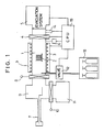
- Fig. 1 is a block diagram showing one embodiment of the inventive impurity doping apparatus.
- the apparatus comprises a vacuum chamber 1 composed of quartz.
- the vacuum chamber 1 is provided to store therein a semiconductor substrate 2 for impurity doping.
- a heating unit 3 is disposed around the vacuum chamber 1 so as to heat the semiconductor substrate 2 by an infrared rays lamp or resistance heater. The heating unit 3 is controlled to regulate a temperature of the semiconductor substrate 2.
- An efficient evacuation system 5 is connected to the vacuum chamber 1 through a gate valve 4.
- the efficient evacuation system 5 comprises a plurality of pumps including a main pump in the form of a turbo molecular pump so as to evacuate the vacuum chamber 1 at high vacuum degree.
- a pressure gauge 6 is provided to continuously monitor the vacuum degree of the chamber 1.
- the impurity doping apparatus is further provided with a transportation mechanism 7 for transporting the substrate 2.
- the transportation mechanism 7 is operated to transport the substrate 2 to the vacuum chamber 1 from a loading chamber 9 which is connected to the chamber 1 through a gate valve 8 which is held open during the transportation of the substrate.
- the loading chamber 9 is normally highly evacuated by a loading chamber evacuation system 11 while opening a gate valve 10 except during the loading of the substrate 2 into the loading chamber 9 and during the transportation of the substrate 2 to the main chamber 1.
- a gas supply source 13 is connected to the vacuum chamber 1 through a gas regulating valve 12.
- the gas supply source 13 is provided with a plurality of bottles for storing various gas species needed for the impurity doping process.
- the gas regulating valve 12 is controlled to regulate gas species, charging amount and charging time of a gas which is introduced from the gas supply source 13 to the reaction chamber 1.
- the gas supply source 13 may contain a reductive gas such as hydrogen gas effective to facilitate the activation treatment of the substrate surface and an impurity gas such as diborane gas which contains an impurity component of boron.
- An analyzer 14 is disposed between the vacuum chamber 1 and the efficient evacuation system 5 for analyzing exhaust gas components.
- the analyzer 14 may be comprised of a quadrupole mass spectrometer.
- a controlling and processing unit 15 including a CPU is connected to control the operation of the heating unit 3, regulating valve 12, gate valve 4, and evacuation system 5.
- the CPU is also connected to the pressure gage 6 and analyzer 14 to effect controlling and processing of the impurity doping apparatus according to detection results from the pressure gage and analyzer.
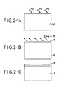
- Fig. 2 - 1 shows a step diagram illustrating an example of a doping process of the impurity boron into a semiconductor substrate 2 such as silicon, by using the inventive impurity doping apparatus.
- step A surface activation treatment is applied to the silicon substrate 2, such that hydrogen gas (H2) is utilized to remove a natural oxide film from the substrate surface by reductive reaction.
- H2 hydrogen gas
- the substrate 2 is simply heated in vacuum to activate the substrate surface.
- the hydrogen gas may be also added to efficiently remove the oxide film.
- a diborane gas 16(B2H6) having an impurity component of boron is introduced into the vacuum chamber while heating the silicon substrate 2 so as to form an impurity adsorption film 17 on the activated surface of the silicon substrate 2.
- the semiconductor substrate 2 is annealed at a given temperature for a given time interval to carry out diffusion treatment of the impurity component into
- the silicon substrate 2 to form an impurity diffusion layer 18.
- Fig. 2 - 2 is a step diagram showing another example in which a silicon substrate 2 is formed with a multi-layer of impurity adsorption film and semiconductor film so as to form an impurity diffusion layer by using the inventive impurity doping apparatus.
- step A surface activation treatment is applied to the silicon substrate 2.
- step B an impurity adsorption film 17 is deposited on the activated surface of the substrate 2.
- step C gas mixture of hydrogen and either of silane(SiH4) or dichlorosilane(SiH2Cl2) is introduced to deposit a semiconductor film 19 on the impurity adsorption film to form a double layer structure.
- the semiconductor substrate 2 is heated to form an impurity diffusion layer 20.
- Fig. 2 - 3 is a step diagram showing a further example in which a gas containing an impurity component and another gas containing a semiconductor component are concurrently applied to a semiconductor substrate 2 made of silicon to facilitate activation of doped impurity component so as to form an impurity diffusion layer having relatively small resistivity, with using the inventive impurity doping apparatus.
- step A surface activation or cleaning treatment is carried out over the silicon substrate 2.
- step B diborane gas containing an impurity component of boron and dichlorosilane containing a semiconductor component of silicon are concurrently applied to the activated surface to from an adsorption film 21 composed of the impurity component and the semiconductor component.
- the semiconductor substrate 2 is annealed to form an impurity diffusion layer 22.
- the doped boron atoms are activated at relatively high rate in the impurity diffusion layer 22 to achieve significantly low resistivity.
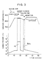
- Fig. 3 is a sequence chart of the impurity doping process showing a sequential procedure given to the controlling and processing unit 15 of the Fig. 1 apparatus to effect sequential treatments illustrated in Fig. 2 - 1.
- the controlling and processing unit 15 comprised of CPU controls the impurity doping apparatus according to the given process sequence or program so as to effect impurity doping.
- the horizontal axis indicates processing time
- the vertical axis indicates a substrate temperature and an interval pressure of the vacuum chamber.
- the substrate 2 is placed in a center of the vacuum chamber 1 which is held at less than 1 x 10 ⁇ 4 Pa of background or base pressure.
- the controlling and processing unit 15 operates according to the given program to control the heating unit 3 to set 850°C of the substrate temperature.
- the gas regulating valve 12 is controlled so that hydrogen gas is introduced from the gas supply source 13 into the vacuum chamber 1.
- the hydrogen gas is charged for a given time interval so that the internal pressure of the vacuum chamber is raised to 1 x 10 ⁇ 2 Pa.
- the internal pressure of the chamber is monitored by the pressure gage 6, and the controlling and processing unit 15 operates according to the monitored results to regulate the gas regulating valve 12.
- a natural oxide film is removed from the surface of the silicon substrate 2 to expose a chemically active silicon face. Namely, the surface of the silicon substrate is cleaned and activated.
- impurity adsorption treatment is effected according to the process sequence program. Namely, after finishing the cleaning of the silicon substrate surface, the controlling and processing unit 15 controls the gas regulating valve 12 to stop the charging of hydrogen gas, and concurrently controls the heating unit to set 825°C of the substrate temperature. After reaching stably the set temperature, the gas regulating valve 12 is controlled so that diborane gas 16 containing the impurity component of boron is charged into the chamber for a given time under the condition that the vacuum chamber pressure is raised to 1 x 10 ⁇ 2 Pa. Consequently, the activated silicon surface is covered with the adsorption film 17 containing boron element or boron compound.
- diffusion treatment is carried out according to the process sequence program. Namely, after finishing the deposition of the impurity adsorption film 17, the regulating valve 12 is controlled to stop charging of the diborane gas. Then, the high evacuation system 5 is operated to highly vacuum the inside of the chamber 1. In this state, the heating unit 3 is controlled to raise the substrate temperature to, for example, 875°C. This heating state is maintained for a given time interval to effect annealing of the substrate to carry out solid-phase diffusion of the impurity component from a diffusion source composed of the impurity adsorption film 17 to thereby form the impurity diffusion layer 18 near the surface of the silicon substrate 2. Concurrently at this treatment, the impurity atoms of boron are activated.
- adsorption amount and annealing condition such as substrate temperature and heating time interval are controlled by the controlling and processing unit 15 so as to form the impurity diffusion layer 18 having a desired impurity concentration and a desired junction depth.
- the adsorption amount of boron can be adjusted to a desired value by controlling the regulating valve 12 to regulate charging pressure and time interval of diborane gas.
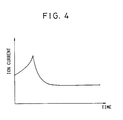
- the analyzer 14 is used to detect an end time of the surface activation or cleaning treatment in the inventive impurity doping apparatus.
- the analyzer 14 is composed, for example, of a quadrupole mass spectrometer for monitoring quantitative change in SiO or H2O contained in the exhaust gas from the vacuum chamber 1 during the course of removing of the natural oxide film on the silicon substrate 2.
- Fig.4 is a graph showing the change in ion current of the quadrupole mass spectrometer, which corresponds to the quantitative change in the exhaust component of SiO. As shown in the graph, when the removal of the natural oxide film progresses on the silicon substrate, the exhaust amount of SiO increases since SiO is released from the silicon substrate.
- the controlling and processing unit 15 can detect the end point of the silicon surface activation treatment while monitoring change in the ion current of the analyzer 14. The controlling and processing unit 15 operates in response to this detection result to control the regulating valve 12 and the heating unit 3 to thereby proceed to the next step of adsorption treatment according to the given process sequence program.
- the inventive impurity doping apparatus features basically that a chemically active semiconductor surface is formed with an adsorption film containing at least an impurity component in the form of a dopant for semiconductor material, and that the impurity doping is effected into the semiconductor from an impurity diffusion source composed of the adsorption film.
- an adsorption film is not substantially deposited on an inert film such as natural oxide film in contrast to active surface of silicon single crystal or polysilicon.
- thermal treatment is carried out after the adsorption treatment, only a trace of the adsorption film remains on the inert film in an amount less than one-tenth of that staying on the active surface.
- the inert film blocks the diffusion of the adsorbed impurity into the bulk of semiconductor. Therefore, it is quite important to carry out activation or cleaning treatment of the substrate surface prior to the adsorption treatment of the impurity.
- the inventive impurity doping apparatus is designed to operate according to a given process sequence program to carry out automatically the activation or cleaning treatment of the semiconductor substrate.
- the inventive impurity doping apparatus is utilized to dope a P type of impurity boron into a silicon substrate by applying diborane gas to the substrate.
- the inventive apparatus may utilize other source compound gases of VII ⁇ ⁇ -group elements such as trimethyl gallium (TMG) and boron trichloride (BCl3) in order to dope the P type of impurity component.
- TMG trimethyl gallium
- BCl3 boron trichloride
- the inventive apparatus can also utilize arsine (AsH3), phosphorus trichloride (PCl3), antimony pentachloride (SbCl5) and phosphine (PH3) in order to dope an N type impurity into the silicon substrate.
- AsH3 arsine
- PCl3 phosphorus trichloride
- SBCl5 antimony pentachloride
- PH3 phosphine
- the doping of impurity can be carried out automatically according to a given process sequence program by the sequential treatments of activating the semiconductor substrate surface, adsorbing the impurity on the activated surface, and diffusing the adsorbed impurity into the semiconductor bulk.
- the inventive apparatus carries out the impurity doping based on the chemical adsorption, thereby achieving advantage that the semiconductor substrate surface is not damaged in contrast to the conventional ion implantation technique. Further, the adsorption amount of impurity can be controlled accurately, thereby achieving advantage that the impurity diffusion density and the diffusion depth can be regulated quite accurately.
- the impurity doping is based on the chemical adsorption, the impurity doping is non-directional to thereby enable formation of uniform diffusion layer over the semiconductor substrate surface.
Applications Claiming Priority (2)
| Application Number | Priority Date | Filing Date | Title |
|---|---|---|---|
| JP1318555A JP2928930B2 (ja) | 1989-12-06 | 1989-12-06 | 不純物ドーピング装置 |
| JP318555/89 | 1989-12-06 |
Publications (2)
| Publication Number | Publication Date |
|---|---|
| EP0438677A2 true EP0438677A2 (fr) | 1991-07-31 |
| EP0438677A3 EP0438677A3 (en) | 1995-07-19 |
Family
ID=18100440
Family Applications (1)
| Application Number | Title | Priority Date | Filing Date |
|---|---|---|---|
| EP90123274A Withdrawn EP0438677A3 (en) | 1989-12-06 | 1990-12-05 | Impurity doping apparatus |
Country Status (5)
| Country | Link |
|---|---|
| US (1) | US5199994A (fr) |
| EP (1) | EP0438677A3 (fr) |
| JP (1) | JP2928930B2 (fr) |
| KR (1) | KR0166587B1 (fr) |
| CA (1) | CA2031418A1 (fr) |
Cited By (1)
| Publication number | Priority date | Publication date | Assignee | Title |
|---|---|---|---|---|
| WO2000039840A1 (fr) * | 1998-12-17 | 2000-07-06 | Vishay Semiconductor Itzehoe Gmbh | Procede de dopage au bore de tranches, mis en oeuvre a l'aide d'un systeme de four vertical |
Families Citing this family (16)
| Publication number | Priority date | Publication date | Assignee | Title |
|---|---|---|---|---|
| JP2892170B2 (ja) * | 1990-07-20 | 1999-05-17 | 株式会社東芝 | 熱処理成膜方法 |
| JP2750063B2 (ja) * | 1991-12-17 | 1998-05-13 | 松下電器産業株式会社 | 半導体界面形成方法 |
| JP2825172B2 (ja) * | 1992-07-10 | 1998-11-18 | 東京エレクトロン株式会社 | 減圧処理装置および減圧処理方法 |
| JPH0897147A (ja) * | 1994-09-29 | 1996-04-12 | Mitsubishi Electric Corp | エピタキシャル結晶成長装置 |
| KR19980053433A (ko) * | 1996-12-26 | 1998-09-25 | 김영환 | 반도체 소자 제조 공정에서의 이온 주입 방법 |
| US6653686B2 (en) | 1998-07-13 | 2003-11-25 | International Business Machines Corporation | Structure and method of controlling short-channel effect of very short channel MOSFET |
| US6468814B1 (en) * | 1998-07-24 | 2002-10-22 | Leybold Inficon, Inc. | Detection of nontransient processing anomalies in vacuum manufacturing process |
| KR100331273B1 (ko) * | 1999-08-07 | 2002-04-06 | 박종섭 | 반도체기판의 표면 처리 방법 |
| DE20110048U1 (de) * | 2001-06-18 | 2001-08-16 | Lambda Physik Ag | Gasentladungslaser mit Mitteln zur Entfernung von Gasverunreinigungen |
| US7238597B2 (en) * | 2002-09-27 | 2007-07-03 | Brontek Delta Corporation | Boron ion delivery system |
| DE10301244B4 (de) * | 2003-01-15 | 2005-03-17 | Infineon Technologies Ag | Verfahren zum Dotieren von Halbleiterkörpern |
| KR100827476B1 (ko) * | 2006-08-29 | 2008-05-06 | 동부일렉트로닉스 주식회사 | 반도체 소자를 제조하기 위한 디가스 챔버 및 이를 이용한디가스 공정 |
| FR2944138B1 (fr) * | 2009-04-06 | 2012-12-07 | Semco Engineering Sa | Procede de dopage au bore de plaquettes de silicium |
| WO2014182333A1 (fr) * | 2013-05-09 | 2014-11-13 | Fomani Arash Akhavan | Pompes à vide destinées à produire des surfaces exemptes d'adsorbat |
| AU2015304774B2 (en) * | 2014-08-21 | 2018-08-30 | Okinawa Institute Of Science And Technology School Corporation | System and method based on low-pressure chemical vapor deposition for fabricating perovskite film |
| US11018225B2 (en) | 2016-06-28 | 2021-05-25 | International Business Machines Corporation | III-V extension by high temperature plasma doping |
Citations (4)
| Publication number | Priority date | Publication date | Assignee | Title |
|---|---|---|---|---|
| US3805736A (en) * | 1971-12-27 | 1974-04-23 | Ibm | Apparatus for diffusion limited mass transport |
| FR2255951A1 (fr) * | 1973-12-26 | 1975-07-25 | Mitsubishi Electric Corp | |
| US4100310A (en) * | 1975-01-20 | 1978-07-11 | Hitachi, Ltd. | Method of doping inpurities |
| JPS58103125A (ja) * | 1981-12-16 | 1983-06-20 | Nec Corp | 加熱制御装置 |
Family Cites Families (5)
| Publication number | Priority date | Publication date | Assignee | Title |
|---|---|---|---|---|
| NL6501786A (fr) * | 1964-02-26 | 1965-08-27 | ||
| JPS58128728A (ja) * | 1982-01-28 | 1983-08-01 | Toshiba Mach Co Ltd | 半導体気相成長装置 |
| US4855258A (en) * | 1987-10-22 | 1989-08-08 | Ncr Corporation | Native oxide reduction for sealing nitride deposition |
| JPH01125821A (ja) * | 1987-11-10 | 1989-05-18 | Matsushita Electric Ind Co Ltd | 気相成長装置 |
| US4940505A (en) * | 1988-12-02 | 1990-07-10 | Eaton Corporation | Method for growing single crystalline silicon with intermediate bonding agent and combined thermal and photolytic activation |
-
1989
- 1989-12-06 JP JP1318555A patent/JP2928930B2/ja not_active Expired - Lifetime
-
1990
- 1990-12-04 CA CA002031418A patent/CA2031418A1/fr not_active Abandoned
- 1990-12-05 EP EP90123274A patent/EP0438677A3/en not_active Withdrawn
- 1990-12-05 KR KR1019900019891A patent/KR0166587B1/ko not_active IP Right Cessation
- 1990-12-06 US US07/623,164 patent/US5199994A/en not_active Expired - Lifetime
Patent Citations (4)
| Publication number | Priority date | Publication date | Assignee | Title |
|---|---|---|---|---|
| US3805736A (en) * | 1971-12-27 | 1974-04-23 | Ibm | Apparatus for diffusion limited mass transport |
| FR2255951A1 (fr) * | 1973-12-26 | 1975-07-25 | Mitsubishi Electric Corp | |
| US4100310A (en) * | 1975-01-20 | 1978-07-11 | Hitachi, Ltd. | Method of doping inpurities |
| JPS58103125A (ja) * | 1981-12-16 | 1983-06-20 | Nec Corp | 加熱制御装置 |
Non-Patent Citations (3)
| Title |
|---|
| PATENT ABSTRACTS OF JAPAN vol. 7 no. 204 (E-197) [1349] ,9 September 1983 & JP-A-58 103125 (NIPPON DENKI K.K.) 20 June 1983, * |
| SOLID STATE TECHNOLOGY, vol. 20,no. 7, July 1977 PORT WASHINGTON, NEW YORK, USA, pages 34-37, D.G.LANDIS ET AL 'AUTOMATIC DIFFUSION FURNACE SYSTEM USING MICROPROCESSOR CONTROL' * |
| SOLID STATE TECHNOLOGY, vol. 27,no. 12, 1984 PORT WASHINGTON, NEW YORK, USA, pages 105-109, J.C. MALIAKAL ET AL 'TRENDS IN AUTOMATED DIFFUSION FURNACE SYSTEMS FOR LARGE WAFERS' * |
Cited By (2)
| Publication number | Priority date | Publication date | Assignee | Title |
|---|---|---|---|---|
| WO2000039840A1 (fr) * | 1998-12-17 | 2000-07-06 | Vishay Semiconductor Itzehoe Gmbh | Procede de dopage au bore de tranches, mis en oeuvre a l'aide d'un systeme de four vertical |
| US6548378B1 (en) | 1998-12-17 | 2003-04-15 | Vishay Semiconductor Itzehoe Gmbh | Method of boron doping wafers using a vertical oven system |
Also Published As
| Publication number | Publication date |
|---|---|
| JP2928930B2 (ja) | 1999-08-03 |
| US5199994A (en) | 1993-04-06 |
| KR910013457A (ko) | 1991-08-08 |
| EP0438677A3 (en) | 1995-07-19 |
| JPH03178126A (ja) | 1991-08-02 |
| CA2031418A1 (fr) | 1991-06-07 |
| KR0166587B1 (ko) | 1999-02-01 |
Similar Documents
| Publication | Publication Date | Title |
|---|---|---|
| EP0438677A2 (fr) | Appareillage pour le dopage d'impuretés | |
| CA2021993C (fr) | Methode de dopage des impuretes et source de diffusion | |
| KR100739837B1 (ko) | 불순물 도입 방법 및 불순물 도입 장치 | |
| US5925574A (en) | Method of producing a bipolar transistor | |
| US6562720B2 (en) | Apparatus and method for surface finishing a silicon film | |
| US5489550A (en) | Gas-phase doping method using germanium-containing additive | |
| KR20010070961A (ko) | 텅스텐 및 텅스텐 질화물의 인 시튜 화학기상증착에 의해개선된 게이트 전극 결합 구조물 | |
| JPH07118471B2 (ja) | 固体平板状拡散源の急速熱処理による半導体ウェ−ハのド−ピング方法 | |
| US5387545A (en) | Impurity diffusion method | |
| EP0430167A2 (fr) | Méthode de fabrication d'un dispositif à jonction PN | |
| JPH11214320A (ja) | 半導体層への不純物領域形成方法及び半導体層への不純物導入装置 | |
| US6077751A (en) | Method of rapid thermal processing (RTP) of ion implanted silicon | |
| EP0430168A2 (fr) | Méthode de dopage des bords d'une tranchée d'un semi-conducteur | |
| US5874352A (en) | Method of producing MIS transistors having a gate electrode of matched conductivity type | |
| JPS6355856B2 (fr) | ||
| JP3180122B2 (ja) | 不純物ドーピングの方法 | |
| EP0684632A2 (fr) | Procédé de fabrication d'un film à basse température pour un dispositif semi-conducteur | |
| EP0430166A2 (fr) | Méthode pour doper des films semi-conducteurs et ruban semi-conducteur configuré | |
| JP2679011B2 (ja) | 不純物原子の導入方法 | |
| EP0505877A2 (fr) | Méthode de dopage à l'aide d'une source de diffusion adsorbée | |
| JPH0436454B2 (fr) | ||
| JPH01129413A (ja) | 半導体基体への不純物導入方法 | |
| JP2876414B2 (ja) | 拡散抵抗素子の製造方法 | |
| JP2926344B2 (ja) | 電界効果トランジスタの製造方法 | |
| JPH03173421A (ja) | 不純物ドーピング方法 |
Legal Events
| Date | Code | Title | Description |
|---|---|---|---|
| PUAI | Public reference made under article 153(3) epc to a published international application that has entered the european phase |
Free format text: ORIGINAL CODE: 0009012 |
|
| AK | Designated contracting states |
Kind code of ref document: A2 Designated state(s): DE FR GB NL |
|
| PUAL | Search report despatched |
Free format text: ORIGINAL CODE: 0009013 |
|
| AK | Designated contracting states |
Kind code of ref document: A3 Designated state(s): DE FR GB NL |
|
| STAA | Information on the status of an ep patent application or granted ep patent |
Free format text: STATUS: THE APPLICATION IS DEEMED TO BE WITHDRAWN |
|
| 18D | Application deemed to be withdrawn |
Effective date: 19960120 |