EP0430168A2 - Méthode de dopage des bords d'une tranchée d'un semi-conducteur - Google Patents
Méthode de dopage des bords d'une tranchée d'un semi-conducteur Download PDFInfo
- Publication number
- EP0430168A2 EP0430168A2 EP90122650A EP90122650A EP0430168A2 EP 0430168 A2 EP0430168 A2 EP 0430168A2 EP 90122650 A EP90122650 A EP 90122650A EP 90122650 A EP90122650 A EP 90122650A EP 0430168 A2 EP0430168 A2 EP 0430168A2
- Authority
- EP
- European Patent Office
- Prior art keywords
- impurity
- trench
- wall
- film
- boron
- Prior art date
- Legal status (The legal status is an assumption and is not a legal conclusion. Google has not performed a legal analysis and makes no representation as to the accuracy of the status listed.)
- Withdrawn
Links
- 239000012535 impurity Substances 0.000 title claims abstract description 96
- 239000004065 semiconductor Substances 0.000 title claims abstract description 36
- 238000000034 method Methods 0.000 title claims description 29
- 239000000758 substrate Substances 0.000 claims abstract description 57
- 238000009792 diffusion process Methods 0.000 claims description 34
- ZOXJGFHDIHLPTG-UHFFFAOYSA-N Boron Chemical compound [B] ZOXJGFHDIHLPTG-UHFFFAOYSA-N 0.000 claims description 32
- XUIMIQQOPSSXEZ-UHFFFAOYSA-N Silicon Chemical compound [Si] XUIMIQQOPSSXEZ-UHFFFAOYSA-N 0.000 claims description 30
- 229910052710 silicon Inorganic materials 0.000 claims description 30
- 239000010703 silicon Substances 0.000 claims description 30
- 229910052796 boron Inorganic materials 0.000 claims description 28
- 238000002955 isolation Methods 0.000 claims description 9
- 238000010438 heat treatment Methods 0.000 claims description 8
- 239000003990 capacitor Substances 0.000 claims description 4
- 238000001179 sorption measurement Methods 0.000 description 22
- 239000007789 gas Substances 0.000 description 21
- 238000010586 diagram Methods 0.000 description 9
- VYPSYNLAJGMNEJ-UHFFFAOYSA-N Silicium dioxide Chemical compound O=[Si]=O VYPSYNLAJGMNEJ-UHFFFAOYSA-N 0.000 description 8
- 238000004140 cleaning Methods 0.000 description 7
- 238000011068 loading method Methods 0.000 description 6
- 150000001875 compounds Chemical class 0.000 description 5
- 239000013078 crystal Substances 0.000 description 4
- 238000001020 plasma etching Methods 0.000 description 4
- UFHFLCQGNIYNRP-UHFFFAOYSA-N Hydrogen Chemical compound [H][H] UFHFLCQGNIYNRP-UHFFFAOYSA-N 0.000 description 3
- 238000000137 annealing Methods 0.000 description 3
- 238000005468 ion implantation Methods 0.000 description 3
- 235000012239 silicon dioxide Nutrition 0.000 description 3
- 229910052814 silicon oxide Inorganic materials 0.000 description 3
- IJGRMHOSHXDMSA-UHFFFAOYSA-N Atomic nitrogen Chemical compound N#N IJGRMHOSHXDMSA-UHFFFAOYSA-N 0.000 description 2
- 229910052581 Si3N4 Inorganic materials 0.000 description 2
- RBFQJDQYXXHULB-UHFFFAOYSA-N arsane Chemical compound [AsH3] RBFQJDQYXXHULB-UHFFFAOYSA-N 0.000 description 2
- 230000015572 biosynthetic process Effects 0.000 description 2
- 238000005229 chemical vapour deposition Methods 0.000 description 2
- 239000011248 coating agent Substances 0.000 description 2
- 238000000576 coating method Methods 0.000 description 2
- 238000000151 deposition Methods 0.000 description 2
- 230000010354 integration Effects 0.000 description 2
- 239000000463 material Substances 0.000 description 2
- FAIAAWCVCHQXDN-UHFFFAOYSA-N phosphorus trichloride Chemical compound ClP(Cl)Cl FAIAAWCVCHQXDN-UHFFFAOYSA-N 0.000 description 2
- 229910021420 polycrystalline silicon Inorganic materials 0.000 description 2
- 229920005591 polysilicon Polymers 0.000 description 2
- 230000001105 regulatory effect Effects 0.000 description 2
- 239000000377 silicon dioxide Substances 0.000 description 2
- HQVNEWCFYHHQES-UHFFFAOYSA-N silicon nitride Chemical compound N12[Si]34N5[Si]62N3[Si]51N64 HQVNEWCFYHHQES-UHFFFAOYSA-N 0.000 description 2
- FAQYAMRNWDIXMY-UHFFFAOYSA-N trichloroborane Chemical compound ClB(Cl)Cl FAQYAMRNWDIXMY-UHFFFAOYSA-N 0.000 description 2
- XCZXGTMEAKBVPV-UHFFFAOYSA-N trimethylgallium Chemical compound C[Ga](C)C XCZXGTMEAKBVPV-UHFFFAOYSA-N 0.000 description 2
- 229910015844 BCl3 Inorganic materials 0.000 description 1
- GRYLNZFGIOXLOG-UHFFFAOYSA-N Nitric acid Chemical compound O[N+]([O-])=O GRYLNZFGIOXLOG-UHFFFAOYSA-N 0.000 description 1
- XYFCBTPGUUZFHI-UHFFFAOYSA-N Phosphine Chemical compound P XYFCBTPGUUZFHI-UHFFFAOYSA-N 0.000 description 1
- QAOWNCQODCNURD-UHFFFAOYSA-N Sulfuric acid Chemical compound OS(O)(=O)=O QAOWNCQODCNURD-UHFFFAOYSA-N 0.000 description 1
- 230000004913 activation Effects 0.000 description 1
- VMPVEPPRYRXYNP-UHFFFAOYSA-I antimony(5+);pentachloride Chemical compound Cl[Sb](Cl)(Cl)(Cl)Cl VMPVEPPRYRXYNP-UHFFFAOYSA-I 0.000 description 1
- 229910000070 arsenic hydride Inorganic materials 0.000 description 1
- 230000004888 barrier function Effects 0.000 description 1
- 150000001638 boron Chemical class 0.000 description 1
- 239000012159 carrier gas Substances 0.000 description 1
- 230000008859 change Effects 0.000 description 1
- 230000001276 controlling effect Effects 0.000 description 1
- 238000005520 cutting process Methods 0.000 description 1
- ZOCHARZZJNPSEU-UHFFFAOYSA-N diboron Chemical compound B#B ZOCHARZZJNPSEU-UHFFFAOYSA-N 0.000 description 1
- 239000002019 doping agent Substances 0.000 description 1
- 238000005516 engineering process Methods 0.000 description 1
- 239000001257 hydrogen Substances 0.000 description 1
- 229910052739 hydrogen Inorganic materials 0.000 description 1
- 239000007943 implant Substances 0.000 description 1
- 150000002500 ions Chemical class 0.000 description 1
- 238000004519 manufacturing process Methods 0.000 description 1
- 230000007246 mechanism Effects 0.000 description 1
- 229910017604 nitric acid Inorganic materials 0.000 description 1
- 229910052757 nitrogen Inorganic materials 0.000 description 1
- 239000010453 quartz Substances 0.000 description 1
- 230000002829 reductive effect Effects 0.000 description 1
- 238000000926 separation method Methods 0.000 description 1
- 238000009751 slip forming Methods 0.000 description 1
- 235000011149 sulphuric acid Nutrition 0.000 description 1
Images


Classifications
-
- H—ELECTRICITY
- H01—ELECTRIC ELEMENTS
- H01L—SEMICONDUCTOR DEVICES NOT COVERED BY CLASS H10
- H01L29/00—Semiconductor devices specially adapted for rectifying, amplifying, oscillating or switching and having potential barriers; Capacitors or resistors having potential barriers, e.g. a PN-junction depletion layer or carrier concentration layer; Details of semiconductor bodies or of electrodes thereof ; Multistep manufacturing processes therefor
- H01L29/66—Types of semiconductor device ; Multistep manufacturing processes therefor
- H01L29/66007—Multistep manufacturing processes
- H01L29/66075—Multistep manufacturing processes of devices having semiconductor bodies comprising group 14 or group 13/15 materials
- H01L29/66083—Multistep manufacturing processes of devices having semiconductor bodies comprising group 14 or group 13/15 materials the devices being controllable only by variation of the electric current supplied or the electric potential applied, to one or more of the electrodes carrying the current to be rectified, amplified, oscillated or switched, e.g. two-terminal devices
- H01L29/66166—Resistors with PN junction
-
- H—ELECTRICITY
- H01—ELECTRIC ELEMENTS
- H01L—SEMICONDUCTOR DEVICES NOT COVERED BY CLASS H10
- H01L21/00—Processes or apparatus adapted for the manufacture or treatment of semiconductor or solid state devices or of parts thereof
- H01L21/02—Manufacture or treatment of semiconductor devices or of parts thereof
- H01L21/04—Manufacture or treatment of semiconductor devices or of parts thereof the devices having potential barriers, e.g. a PN junction, depletion layer or carrier concentration layer
- H01L21/18—Manufacture or treatment of semiconductor devices or of parts thereof the devices having potential barriers, e.g. a PN junction, depletion layer or carrier concentration layer the devices having semiconductor bodies comprising elements of Group IV of the Periodic Table or AIIIBV compounds with or without impurities, e.g. doping materials
- H01L21/22—Diffusion of impurity materials, e.g. doping materials, electrode materials, into or out of a semiconductor body, or between semiconductor regions; Interactions between two or more impurities; Redistribution of impurities
- H01L21/225—Diffusion of impurity materials, e.g. doping materials, electrode materials, into or out of a semiconductor body, or between semiconductor regions; Interactions between two or more impurities; Redistribution of impurities using diffusion into or out of a solid from or into a solid phase, e.g. a doped oxide layer
- H01L21/2251—Diffusion into or out of group IV semiconductors
- H01L21/2254—Diffusion into or out of group IV semiconductors from or through or into an applied layer, e.g. photoresist, nitrides
-
- H—ELECTRICITY
- H01—ELECTRIC ELEMENTS
- H01L—SEMICONDUCTOR DEVICES NOT COVERED BY CLASS H10
- H01L21/00—Processes or apparatus adapted for the manufacture or treatment of semiconductor or solid state devices or of parts thereof
- H01L21/70—Manufacture or treatment of devices consisting of a plurality of solid state components formed in or on a common substrate or of parts thereof; Manufacture of integrated circuit devices or of parts thereof
- H01L21/71—Manufacture of specific parts of devices defined in group H01L21/70
- H01L21/76—Making of isolation regions between components
- H01L21/762—Dielectric regions, e.g. EPIC dielectric isolation, LOCOS; Trench refilling techniques, SOI technology, use of channel stoppers
- H01L21/76224—Dielectric regions, e.g. EPIC dielectric isolation, LOCOS; Trench refilling techniques, SOI technology, use of channel stoppers using trench refilling with dielectric materials
- H01L21/76237—Dielectric regions, e.g. EPIC dielectric isolation, LOCOS; Trench refilling techniques, SOI technology, use of channel stoppers using trench refilling with dielectric materials introducing impurities in trench side or bottom walls, e.g. for forming channel stoppers or alter isolation behavior
-
- H—ELECTRICITY
- H01—ELECTRIC ELEMENTS
- H01L—SEMICONDUCTOR DEVICES NOT COVERED BY CLASS H10
- H01L29/00—Semiconductor devices specially adapted for rectifying, amplifying, oscillating or switching and having potential barriers; Capacitors or resistors having potential barriers, e.g. a PN-junction depletion layer or carrier concentration layer; Details of semiconductor bodies or of electrodes thereof ; Multistep manufacturing processes therefor
- H01L29/66—Types of semiconductor device ; Multistep manufacturing processes therefor
- H01L29/66007—Multistep manufacturing processes
- H01L29/66075—Multistep manufacturing processes of devices having semiconductor bodies comprising group 14 or group 13/15 materials
- H01L29/66083—Multistep manufacturing processes of devices having semiconductor bodies comprising group 14 or group 13/15 materials the devices being controllable only by variation of the electric current supplied or the electric potential applied, to one or more of the electrodes carrying the current to be rectified, amplified, oscillated or switched, e.g. two-terminal devices
- H01L29/66181—Conductor-insulator-semiconductor capacitors, e.g. trench capacitors
Definitions
- the present invention relates to the method of doping an impurity into a side wall of trench or groove formed on a surface of a semiconductor substrate.
- the semiconductor surface is formed with a trench, and a semiconductor resistive element or a semiconductor capacitive element is formed in the trench in order to improve integration density of the semiconductor device. Further, it is known that such trench is utilized to form a device isolation region. An impurity is diffused into side walls of a trench in order to form the semiconductor elements or device isolation region. Conventionally, such doping of impurity is carried out by ion implantation or so-called predeposition to the side walls.
- the ion implantation is effected to accelerate impurity ions to implant the same, hence the doping is necessarily directional. Therefore, the ion implantation has drawbacks that the impurity cannot be doped into the entire area of the side walls in a trench with uniform density and uniform diffusion depth.
- the conventional predeposition is effected by diffusing impurity through an inert film barrier such as silicon dioxide coated on the trench side walls, hence the predeposition has the drawbacks that it would be difficult to control the impurity density and diffusion depth.
- an object of the invention is to provide a new method of doping an impurity uniformly and continuously into side walls of the trench.
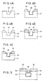
- Figs. 1A-1D are a process step diagram showing the inventive impurity doping method
- Fig. 2 is a block diagram showing a processing apparatus for use in the impurity doping
- Fig. 3 is a graph showing a peak density change of the doped boron
- Figs. 4A-4E are a process step diagram showing the method of producing a trench resistive element
- Fig. 5 is a sectional view of another trench resistive element
- Figs. 6A-6E are a process step diagram showing the method of forming a trench device isolation region.
- Fig. 7 is a sectional diagram of a trench capacitive element.
- Figs. 1A-1D are a process step diagram showing the basic method of doping an impurity into a trench wall.
- a semiconductor substrate 1 is formed thereon with a groove 2.
- the groove 2 is shaped, for example, in the form of a trench having an inner wall 3.
- the inner wall 3 includes side walls and bottom wall of the groove 2.
- the inner wall 3 is naturally covered with an inert film 4.
- the inert film is removed from a surface of the inner wall 3 to expose an active surface.
- the semiconductor substrate 1 is composed of silicon
- the inert film 4 is composed of a silicon oxide coating.
- the groove 2 or trench is generally formed by means of reactive ion etching.
- the inner wall 3 is immediately covered by an inert film after completion of the reactive ion etching treatment. Therefore, the Fig. 1B step is needed to clean the inner wall 3 of the groove 2 to expose an active surface.
- This cleaning treatment is carried out by heating the semiconductor substrate 1 in high vacuum condition.
- a reductive gas such as hydrogen may be concurrently introduced to facilitate the cleaning treatment.
- a source gas such as diborane which contains an impurity component in the form of boron atoms is applied to the exposed active surface so as to adsorb a compound composed of or containing the impurity component to form an impurity film 5.
- This adsorption treatment is carried out by introducing the diborane gas into a high vacuum chamber with a predetermined pressure. This impurity film 5 is selectively adsorbed substantially only onto the active surface.
- the semiconductor substrate 1 is heated so as to diffuse the impurity, i.e., boron which constitutes the impurity film 5 into the inner wall 3 and to activate the impurity. Consequently, the impurity diffusion layer 6 is formed along the inner wall 3.
- This impurity diffusion layer 6 has a desired electric conductivity and impurity diffusion density controlled by regulating an amount of the adsorbed impurity atoms and a heating time interval.
- Such impurity diffusion layer 6 can be utilized as a resistive layer, an electrode layer or an electrically isolating layer.
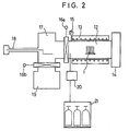
- Fig. 2 is a block diagram showing a doping apparatus for practicing the impurity doping method according to the invention.
- the apparatus is comprised of a chamber 12 made of quartz, and a silicon substrate 1 is disposed in a central portion of the chamber 12.
- the silicon substrate 1 is formed with a trench beforehand, and the substrate 1 is covered by a mask over its surface except the trench inner wall.
- the substrate temperature is regulated by a heating system 13 utilizing an infrared ray lamp heater or a resistance heater so as to maintain the substrate temperature at a predetermined degree.
- the chamber 12 can be evacuated to high vacuum degree by means of an efficient vacuum system 14 composed of plural pumps including a main vacuum pump in the form of a turbo molecular pump.
- a vacuum degree of the chamber 12 is continuously monitored by a pressure gage 15.
- the silicon substrate 1 is transported by means of a transporting mechanism 18 to the chamber 12 from a loading chamber 17 which is connected to the chamber 12 through a gate value 16a which is held open during the transportation.
- the loading chamber 17 is normally evacuated by means of a loading chamber vacuum system 19 through an opened gate value 16b except when loading the silicon substrate 1 into the loading chamber 17 and transporting the same from the loading chamber 17.
- a gas supply source 21 is connected to the chamber 12 through a gas flow control system 20.
- the gas supply source 21 contains a plurality of bottles for storing various gas materials needed for doping of the impurity.
- the gas species, charging pressure and application time interval can be controlled by the gas flow control system 20 when charging gases from the supply source 21 to the chamber 12.
- the cleaning treatment is carried out for the inner wall 3 of the trench 2 formed on the silicon substrate 1.
- the silicon substrate 1 is placed in a central portion of the vacuum chamber 12 maintained below 1 x 10 ⁇ 4 Pa of the background pressure.
- the silicon substrate 1 is heated to 850°C, and hydrogen gas is introduced for a predetermined period into the chamber 12 under the condition that the chamber pressure is raised to 1.3 x 10 ⁇ 2 Pa.
- the natural oxide film 4 is removed from the inner wall 3 formed in the silicon substrate surface to expose a chemically active surface.
- the activated inner wall is deposited with an adsorption layer composed of boron element or compound containing boron atoms.
- the hydrogen gas is stopped and the substrate temperature is lowered to, for example, 800°C.
- the chamber 12 is filled with diborane ( B2H6 )gas which contains boron and is dilluted to 5% with nitrogen carrier gas for a predetermined time interval under the chamber pressure condition of 1.3 x 10 ⁇ 2 Pa. Consequently, an adsorption layer composed of boron element or boron-containing compound is deposited on the activated inner wall 3 of the groove formed on the silicon substrate 1.
- a part of boron atoms may be diffused into the bulk of silicon substrate 1 by a certain rate determined according to the substrate temperature and diborane gas pressure during the charging of the diborane. Then, heating treatment or annealing is carried out for the silicon substrate 1.
- the diborane gas is stopped and the substrate is heated for a predetermined time in the vacuum chamber 12.
- the substrate temperature may be preferably set slightly higher than that during the impurity adsorption treatment.
- the impurity diffusion layer 6 is formed along the inner wall 3 from a diffusion source composed of the boron impurity film 5, and concurrently the diffused boron atoms are partly activated.
- the amount of adsorbed boron and the annealing condition may be controlled to form an impurity diffusion layer having a desired impurity concentration and diffusion depth.
- Fig. 3 is a graph showing the dependency of the doped boron peak density on the diborane charging time interval while the diborane charging pressure is set as a parameter.
- the greater the charging pressure of diborane gas the greater the amount of adsorbed boron, thereby increasing the peak density of the doped boron.
- the longer the charging time interval of the diborane gas the more the amount of adsorbed boron, thereby increasing the peak density of the doped boron. Therefore, by suitably setting the charging pressure and interval of the diborane, the boron peak density can be desirably controlled in the impurity diffusion layer. Consequently, the thus obtained boron diffusion layer can be applied for various uses.
- the inventive method is characterized basically in that a semiconductor trench wall is chemically activated, and then an adsorption layer composed of an impurity element acting as a dopant for the semiconductor material is formed on the activated surface of the trench wall, and thereafter the impurity doping is effected into the semiconductor trench wall from an impurity diffusion source in the form of the adsorption layer.
- an adsorption layer is not formed substantially on an inactive surface covered by the oxide film in contrast to the active surface, or the adsorbed impurity may remain on the inactive surface only one-tenth or less of that adsorbed on the active surface.
- doping of the P type impurity can be effected to the trench wall of silicon semiconductor substrate by using various source gases of compound composed of VI-group elements such as trimethyl gallium (TMG) and trichloroboron ( BCl3 ).
- TMG trimethyl gallium
- BCl3 trichloroboron
- doping of the N type impurity can be effected to the trench wall of silicon semiconductor substrate by using various source gases such as arsine ( AsH3 ), phosphorus trichloride ( PCl3 ), antimony pentachloride ( SbCl5 ) and phosphine (PH3).
- the substrate temperature should be preferably set in the range from 800°C to 1200°C dependently on the background pressure and ambient gas species for effecting cleaning treatment of the semiconductor trench wall.
- the substrate temperature should be preferably set in the range from 400°C to 950°C for carrying out the adsorption treatment.
- a silicon single crystal film may be formed on the impurity adsorption film by means of epitaxial growth method.
- an impurity adsorption film and a silicon single crystal film may be superposed with one another so as to form an impurity diffusion layer.
- the silicon single crystal film is interposed so as to advantageously facilitate activation of the impurity.
- the impurity adsorption film and the silicon single crystal film are superposed repeatedly so as to suitably control the thickness of the impurity diffusion layer.
- adsorption and diffusion of the impurity may be repeatedly carried out to form an impurity diffusion layer having desired impurity concentration, junction depth and impurity profile.
- Figs. 4A-4E are a process step diagram showing the method of producing a trench resistive element according to the inventive impurity doping method.
- a semiconductor substrate 41 is composed of silicon, and a trench 42 is formed thereon, having an inner wall 43.
- the formation of trench 42 can be carried out, for example, by reactive ion etching.
- an insulating film 44 is formed on the substrate along edges of the trench 42 so as to mask a semiconductor region other than that to be doped with impurity.
- the insulating film 44 is provided by depositing a silicon oxide film or silicon nitride film, for example, by means of chemical vapor deposition method.
- Fig. 4C cleaning treatment is carried out to exposed surface areas of the trench inner wall 43 and silicon substrate 41 so as to remove an inert film to thereby expose an active surface.
- diborane gas is applied to the active surface to selectively form an impurity adsorption film 45 containing boron.
- the adsorption of the impurity film 45 is chemically effected so that the impurity film 45 is deposited along the exposed surface areas of the trench inner wall 43 and silicon substrate 41 in uniform thickness.
- the substrate 41 is heated so that the impurity boron is diffused uniformly from the adsorption film 45 into the trench inner wall and the exposed surface of silicon substrate to thereby form an impurity diffusion layer 46.
- This impurity diffusion layer 46 is of P + type and has a desired resistivity by controlling the amount of adsorption of the impurity boron. Further, the impurity diffusion layer 46 is uniformly and continuously formed along the trench wall 43 to provide an excellent resistive layer.
- a pair of electrode layers 47 are formed opposite sides of the trench to form a so-called trench resistor.
- the resistor can be formed in the trench so as to facilitate miniaturization of a semiconductor device. If a resistive layer is formed on the trench wall by means of the conventional predeposition technology, there would be caused practical drawbacks such as cutting of the resistive film and variation of the resistive layer thickness.
- Fig. 5 shows another type of the trench resistor produced by the inventive impurity doping method.
- the trench resistor has a cavity 52 formed in a surface of a silicon semiconductor substrate 51.
- This cavity 52 has an upper neck portion and a lower enlarged portion so as to three-dimensionally and more efficiently use the semiconductor substrate area.
- An impurity diffusion layer 53 is formed along an inner wall of the cavity 52.
- a pair of electrode layers 55 are formed on opposite sides of the cavity 52 through an insulating film 54. These pair of electrodes 55 are connected at their end portions to the impurity diffusion layer 53 to constitute a trench resistor.
- Figs. 6A-6E show a fabrication step diagram of a so-called trench device isolation region formed by the inventive impurity doping method.
- a semiconductor substrate 61 composed of silicon is formed thereon with an insulating layer 62, which is composed of a silicon oxide layer or silicon nitride layer.
- the insulating layer 62 is coated by a resist film 63.
- the resist film 63 is etched with a predetermined pattern to remove a part thereof. This partly removed portion defines a device separation region.
- Fig. 6B reactive ion etching is carried out through the resist film 63 to form a trench 64 in the substrate 61. Subsequently, the resist film 63 is removed by H2SO4 or HNO3 or dry removing.
- an impurity adsorption film 65 of boron is selectively formed only on the trench inner wall.
- this boron adsorption treatment is carried out by applying diborane gas to the substrate 61 while heating the same.
- the substrate 61 is annealed so that boron atoms contained in the impurity adsorption film 65 are diffused into the semiconductor substrate 61 through the trench inner surface and are activated in the substrate. Consequently, a P type of impurity diffusion layer 66 is formed at relatively high concentration. This impurity diffusion layer 66 is provided to uniformly and completely cover the trench.
- the trench 64 is filled with an oxide layer 67, thereby completing a trench device isolation region.
- This trench device isolation region has a double layer structure composed of the filled oxide layer 67 and the impurity diffusion layer 66.
- the impurity diffusion layer 66 of high density P type is interposed between the semiconductor substrate 61 and the oxide layer 67 so as to efficiently ensure the isolation of adjacent device. Stated otherwise, the impurity diffusion layer 66 functions to avoid inversion of the semiconductor layer in the vicinity of the boundary to thereby significantly raise a threshold voltage of the trench isolation region.
- Fig. 7 shows a trench capacitor fabricated according to the inventive impurity doping method.
- the trench capacitor is formed in a silicon semiconductor substrate 71 of the N type.
- the substrate 71 has therein a trench, and a P + type of electrode layer 72 is formed along an inner wall of the trench.
- This electrode layer 72 is formed according to the inventive impurity doping method in the form of a P + type impurity diffusion layer which contains boron.
- a dielectric layer 73 is formed along the electrode layer 72.
- This dielectric layer 73 is deposited by chemical vapor deposition of silicon dioxide.
- Another electrode layer 74 is formed on the dielectric layer 73.
- This electrode layer 74 is provided by depositing a polysilicon layer and by doping heavily an impurity into the polysilicon layer. According to this embodiment, the trench capacitor can be easily formed in the surface portion of the semiconductor substrate, thereby improving integration density of a semiconductor device.
- an impurity diffusion layer can be formed uniformly and continuously along an inner wall of a trench formed in a surface portion of a semiconductor substrate by sequence of the cleaning treatment of the inner wall, the impurity adsorption treatment and the diffusion treatment. Further, impurity density and junction depth between the diffusion layer and the silicon substrate can be easily controlled in the impurity diffusion layer, so that the thus obtained impurity diffusion layer can be applied advantageously to various uses.
Landscapes
- Engineering & Computer Science (AREA)
- Power Engineering (AREA)
- Microelectronics & Electronic Packaging (AREA)
- Manufacturing & Machinery (AREA)
- Physics & Mathematics (AREA)
- Condensed Matter Physics & Semiconductors (AREA)
- General Physics & Mathematics (AREA)
- Computer Hardware Design (AREA)
- Ceramic Engineering (AREA)
- Semiconductor Integrated Circuits (AREA)
Applications Claiming Priority (2)
| Application Number | Priority Date | Filing Date | Title |
|---|---|---|---|
| JP313722/89 | 1989-12-01 | ||
| JP01313722A JP3130906B2 (ja) | 1989-12-01 | 1989-12-01 | 半導体内壁に対する不純物の注入方法 |
Publications (2)
| Publication Number | Publication Date |
|---|---|
| EP0430168A2 true EP0430168A2 (fr) | 1991-06-05 |
| EP0430168A3 EP0430168A3 (en) | 1993-05-12 |
Family
ID=18044730
Family Applications (1)
| Application Number | Title | Priority Date | Filing Date |
|---|---|---|---|
| EP19900122650 Withdrawn EP0430168A3 (en) | 1989-12-01 | 1990-11-27 | Doping method of impurity into semiconductor trench wall |
Country Status (3)
| Country | Link |
|---|---|
| EP (1) | EP0430168A3 (fr) |
| JP (1) | JP3130906B2 (fr) |
| CA (1) | CA2031252A1 (fr) |
Cited By (9)
| Publication number | Priority date | Publication date | Assignee | Title |
|---|---|---|---|---|
| EP0628213A1 (fr) * | 1992-02-25 | 1994-12-14 | Ag Associates, Inc. | Dopage en phase gazeuse et a une pression reduite d'un materiau semi-conducteur dans un reacteur a parois froides chauffe par rayonnement |
| DE4404757A1 (de) * | 1994-02-15 | 1995-08-17 | Siemens Ag | Verfahren zur Herstellung eines einem Graben benachbarten Diffusionsgebietes in einem Substrat |
| US5656511A (en) * | 1989-09-04 | 1997-08-12 | Canon Kabushiki Kaisha | Manufacturing method for semiconductor device |
| US5700712A (en) * | 1993-06-23 | 1997-12-23 | Siemens Aktiengesellschaft | Method for manufacturing an insulating trench in an SOI substrate for smartpower technologies |
| EP1979949A2 (fr) * | 2006-01-09 | 2008-10-15 | International Business Machines Corporation | Structure à semiconducteur comprenant un condensateur de tranchée et une résistance de tranchée |
| US7547619B2 (en) | 2002-09-20 | 2009-06-16 | Panasonic Corporation | Method of introducing impurity, device and element |
| WO2010003928A2 (fr) * | 2008-07-06 | 2010-01-14 | Interuniversitair Microelektronica Centrum Vzw (Imec) | Procédé de dopage de structures semi-conductrices et dispositif semi-conducteur associé |
| WO2011015397A1 (fr) * | 2009-08-05 | 2011-02-10 | Robert Bosch Gmbh | Transistor à effet de champ à diode tjbs intégrée |
| DE10112783B4 (de) * | 2000-03-16 | 2011-02-24 | DENSO CORPORATION, Kariya-shi | Halbleiteranordnung mit einem Leistungs-MOSFET und einem Widerstandselement |
Families Citing this family (1)
| Publication number | Priority date | Publication date | Assignee | Title |
|---|---|---|---|---|
| JP6564689B2 (ja) * | 2015-11-06 | 2019-08-21 | 東京エレクトロン株式会社 | 熱処理システム、熱処理方法、及び、プログラム |
Citations (5)
| Publication number | Priority date | Publication date | Assignee | Title |
|---|---|---|---|---|
| JPS63239939A (ja) * | 1987-03-27 | 1988-10-05 | Toshiba Corp | 半導体基体内への不純物導入方法及び装置 |
| US4791074A (en) * | 1986-08-29 | 1988-12-13 | Kabushiki Kaisha Toshiba | Method of manufacturing a semiconductor apparatus |
| EP0316165A2 (fr) * | 1987-11-11 | 1989-05-17 | Seiko Instruments Inc. | Procédé d'isolation par rainures |
| US4861729A (en) * | 1987-08-24 | 1989-08-29 | Matsushita Electric Industrial Co., Ltd. | Method of doping impurities into sidewall of trench by use of plasma source |
| JPH1192159A (ja) * | 1997-09-22 | 1999-04-06 | Matsushita Electric Ind Co Ltd | ガラス基板の製造方法及びその装置 |
-
1989
- 1989-12-01 JP JP01313722A patent/JP3130906B2/ja not_active Expired - Lifetime
-
1990
- 1990-11-27 EP EP19900122650 patent/EP0430168A3/en not_active Withdrawn
- 1990-11-30 CA CA 2031252 patent/CA2031252A1/fr not_active Abandoned
Patent Citations (5)
| Publication number | Priority date | Publication date | Assignee | Title |
|---|---|---|---|---|
| US4791074A (en) * | 1986-08-29 | 1988-12-13 | Kabushiki Kaisha Toshiba | Method of manufacturing a semiconductor apparatus |
| JPS63239939A (ja) * | 1987-03-27 | 1988-10-05 | Toshiba Corp | 半導体基体内への不純物導入方法及び装置 |
| US4861729A (en) * | 1987-08-24 | 1989-08-29 | Matsushita Electric Industrial Co., Ltd. | Method of doping impurities into sidewall of trench by use of plasma source |
| EP0316165A2 (fr) * | 1987-11-11 | 1989-05-17 | Seiko Instruments Inc. | Procédé d'isolation par rainures |
| JPH1192159A (ja) * | 1997-09-22 | 1999-04-06 | Matsushita Electric Ind Co Ltd | ガラス基板の製造方法及びその装置 |
Non-Patent Citations (2)
| Title |
|---|
| PATENT ABSTRACTS OF JAPAN vol. 13, no. 44 (E-710)31 January 1989 & JP-A-63 239 939 ( TOSHIBA CORP ) 5 October 1988 * |
| PATENT ABSTRACTS OF JAPAN vol. 13, no. 483 (E-839)2 November 1989 & JP-A-11 92 159 ( MITSUBISHI ELECTRIC CORP ) 2 August 1989 * |
Cited By (18)
| Publication number | Priority date | Publication date | Assignee | Title |
|---|---|---|---|---|
| US5656511A (en) * | 1989-09-04 | 1997-08-12 | Canon Kabushiki Kaisha | Manufacturing method for semiconductor device |
| EP0628213A1 (fr) * | 1992-02-25 | 1994-12-14 | Ag Associates, Inc. | Dopage en phase gazeuse et a une pression reduite d'un materiau semi-conducteur dans un reacteur a parois froides chauffe par rayonnement |
| EP0628213A4 (fr) * | 1992-02-25 | 1997-02-19 | Processing Technology Inc D B | Dopage en phase gazeuse et a une pression reduite d'un materiau semi-conducteur dans un reacteur a parois froides chauffe par rayonnement. |
| US5700712A (en) * | 1993-06-23 | 1997-12-23 | Siemens Aktiengesellschaft | Method for manufacturing an insulating trench in an SOI substrate for smartpower technologies |
| DE4404757A1 (de) * | 1994-02-15 | 1995-08-17 | Siemens Ag | Verfahren zur Herstellung eines einem Graben benachbarten Diffusionsgebietes in einem Substrat |
| US5726094A (en) * | 1994-02-15 | 1998-03-10 | Siemens Aktiengesellschaft | Process for producing a diffusion region adjacent to a recess in a substrate |
| DE4404757C2 (de) * | 1994-02-15 | 1998-08-20 | Siemens Ag | Verfahren zur Herstellung eines einem Graben benachbarten Diffusionsgebietes in einem Substrat |
| DE10112783B4 (de) * | 2000-03-16 | 2011-02-24 | DENSO CORPORATION, Kariya-shi | Halbleiteranordnung mit einem Leistungs-MOSFET und einem Widerstandselement |
| US7547619B2 (en) | 2002-09-20 | 2009-06-16 | Panasonic Corporation | Method of introducing impurity, device and element |
| EP1979949A4 (fr) * | 2006-01-09 | 2010-08-25 | Ibm | Structure à semiconducteur comprenant un condensateur de tranchée et une résistance de tranchée |
| EP1979949A2 (fr) * | 2006-01-09 | 2008-10-15 | International Business Machines Corporation | Structure à semiconducteur comprenant un condensateur de tranchée et une résistance de tranchée |
| US8110862B2 (en) | 2006-01-09 | 2012-02-07 | International Business Machines Corporation | Semiconductor structure including trench capacitor and trench resistor |
| WO2010003928A2 (fr) * | 2008-07-06 | 2010-01-14 | Interuniversitair Microelektronica Centrum Vzw (Imec) | Procédé de dopage de structures semi-conductrices et dispositif semi-conducteur associé |
| WO2010003928A3 (fr) * | 2008-07-06 | 2010-05-06 | Interuniversitair Microelektronica Centrum Vzw (Imec) | Procédé de dopage de structures semi-conductrices et dispositif semi-conducteur associé |
| US8507337B2 (en) | 2008-07-06 | 2013-08-13 | Imec | Method for doping semiconductor structures and the semiconductor device thereof |
| US8962369B2 (en) | 2008-07-06 | 2015-02-24 | Imec | Method for doping semiconductor structures and the semiconductor device thereof |
| WO2011015397A1 (fr) * | 2009-08-05 | 2011-02-10 | Robert Bosch Gmbh | Transistor à effet de champ à diode tjbs intégrée |
| CN102473725A (zh) * | 2009-08-05 | 2012-05-23 | 罗伯特·博世有限公司 | 带有集成tjbs二极管的场效应晶体管 |
Also Published As
| Publication number | Publication date |
|---|---|
| EP0430168A3 (en) | 1993-05-12 |
| JP3130906B2 (ja) | 2001-01-31 |
| JPH03173420A (ja) | 1991-07-26 |
| CA2031252A1 (fr) | 1991-06-02 |
Similar Documents
| Publication | Publication Date | Title |
|---|---|---|
| US5925574A (en) | Method of producing a bipolar transistor | |
| US5064775A (en) | Method of fabricating an improved polycrystalline silicon thin film transistor | |
| US5366922A (en) | Method for producing CMOS transistor | |
| CA2021993C (fr) | Methode de dopage des impuretes et source de diffusion | |
| US5338697A (en) | Doping method of barrier region in semiconductor device | |
| EP0329482A2 (fr) | Procédé pour fabriquer un transistor à couche mince | |
| EP0430168A2 (fr) | Méthode de dopage des bords d'une tranchée d'un semi-conducteur | |
| US5256162A (en) | Apparatus for forming shallow electrical junctions | |
| JP2928930B2 (ja) | 不純物ドーピング装置 | |
| JP3079575B2 (ja) | 半導体装置の製造方法 | |
| JP2906260B2 (ja) | Pn接合素子の製造方法 | |
| US5874352A (en) | Method of producing MIS transistors having a gate electrode of matched conductivity type | |
| EP0430166A2 (fr) | Méthode pour doper des films semi-conducteurs et ruban semi-conducteur configuré | |
| JP3263058B2 (ja) | 半導体内壁に対する不純物の注入方法 | |
| JP2926344B2 (ja) | 電界効果トランジスタの製造方法 | |
| JP3023481B2 (ja) | 半導体膜に対する不純物の注入方法 | |
| EP0431616A2 (fr) | Méthode de fabrication d'un transistor CMOS | |
| JP2928929B2 (ja) | 不純物ドーピング方法 | |
| US4373975A (en) | Method of diffusing an impurity | |
| JP2973011B2 (ja) | 半導体素子分離領域の形成方法 | |
| JP2876414B2 (ja) | 拡散抵抗素子の製造方法 | |
| JP2934665B2 (ja) | 半導体装置の製造方法 | |
| JPH03178127A (ja) | Soi基板の製造方法 | |
| JP2867046B2 (ja) | 相補型絶縁ゲート電界効果トランジスタの製法 | |
| GB2202086A (en) | Annealing gallium arsenide substrates |
Legal Events
| Date | Code | Title | Description |
|---|---|---|---|
| PUAI | Public reference made under article 153(3) epc to a published international application that has entered the european phase |
Free format text: ORIGINAL CODE: 0009012 |
|
| AK | Designated contracting states |
Kind code of ref document: A2 Designated state(s): DE FR GB |
|
| PUAL | Search report despatched |
Free format text: ORIGINAL CODE: 0009013 |
|
| AK | Designated contracting states |
Kind code of ref document: A3 Designated state(s): DE FR GB |
|
| 17P | Request for examination filed |
Effective date: 19931109 |
|
| 17Q | First examination report despatched |
Effective date: 19940830 |
|
| STAA | Information on the status of an ep patent application or granted ep patent |
Free format text: STATUS: THE APPLICATION IS DEEMED TO BE WITHDRAWN |
|
| 18D | Application deemed to be withdrawn |
Effective date: 19950929 |