JP6564689B2 - 熱処理システム、熱処理方法、及び、プログラム - Google Patents
熱処理システム、熱処理方法、及び、プログラム Download PDFInfo
- Publication number
- JP6564689B2 JP6564689B2 JP2015218054A JP2015218054A JP6564689B2 JP 6564689 B2 JP6564689 B2 JP 6564689B2 JP 2015218054 A JP2015218054 A JP 2015218054A JP 2015218054 A JP2015218054 A JP 2015218054A JP 6564689 B2 JP6564689 B2 JP 6564689B2
- Authority
- JP
- Japan
- Prior art keywords
- heat treatment
- impurity
- thin film
- diffusion
- model
- Prior art date
- Legal status (The legal status is an assumption and is not a legal conclusion. Google has not performed a legal analysis and makes no representation as to the accuracy of the status listed.)
- Active
Links
- 238000010438 heat treatment Methods 0.000 title claims description 149
- 238000000034 method Methods 0.000 title claims description 89
- 239000010408 film Substances 0.000 claims description 103
- 238000009792 diffusion process Methods 0.000 claims description 86
- 239000012535 impurity Substances 0.000 claims description 85
- 230000008569 process Effects 0.000 claims description 75
- 239000010409 thin film Substances 0.000 claims description 75
- 238000003860 storage Methods 0.000 claims description 63
- 230000008859 change Effects 0.000 claims description 45
- 238000004364 calculation method Methods 0.000 claims description 18
- 238000003672 processing method Methods 0.000 claims description 3
- 239000007789 gas Substances 0.000 description 66
- 229910021420 polycrystalline silicon Inorganic materials 0.000 description 44
- 229920005591 polysilicon Polymers 0.000 description 44
- 238000006243 chemical reaction Methods 0.000 description 39
- 235000012431 wafers Nutrition 0.000 description 31
- 238000004519 manufacturing process Methods 0.000 description 24
- 239000004065 semiconductor Substances 0.000 description 16
- 239000010410 layer Substances 0.000 description 15
- OAICVXFJPJFONN-UHFFFAOYSA-N Phosphorus Chemical compound [P] OAICVXFJPJFONN-UHFFFAOYSA-N 0.000 description 7
- 229910052698 phosphorus Inorganic materials 0.000 description 7
- 239000011574 phosphorus Substances 0.000 description 7
- 239000002344 surface layer Substances 0.000 description 7
- 239000012528 membrane Substances 0.000 description 5
- 238000004891 communication Methods 0.000 description 4
- 230000006870 function Effects 0.000 description 4
- 238000005259 measurement Methods 0.000 description 4
- 230000004913 activation Effects 0.000 description 3
- 238000000137 annealing Methods 0.000 description 3
- 230000015572 biosynthetic process Effects 0.000 description 3
- 239000000758 substrate Substances 0.000 description 3
- 229910000577 Silicon-germanium Inorganic materials 0.000 description 2
- 229910021417 amorphous silicon Inorganic materials 0.000 description 2
- 238000005457 optimization Methods 0.000 description 2
- ZOXJGFHDIHLPTG-UHFFFAOYSA-N Boron Chemical compound [B] ZOXJGFHDIHLPTG-UHFFFAOYSA-N 0.000 description 1
- OKTJSMMVPCPJKN-UHFFFAOYSA-N Carbon Chemical compound [C] OKTJSMMVPCPJKN-UHFFFAOYSA-N 0.000 description 1
- UOACKFBJUYNSLK-XRKIENNPSA-N Estradiol Cypionate Chemical compound O([C@H]1CC[C@H]2[C@H]3[C@@H](C4=CC=C(O)C=C4CC3)CC[C@@]21C)C(=O)CCC1CCCC1 UOACKFBJUYNSLK-XRKIENNPSA-N 0.000 description 1
- LEVVHYCKPQWKOP-UHFFFAOYSA-N [Si].[Ge] Chemical compound [Si].[Ge] LEVVHYCKPQWKOP-UHFFFAOYSA-N 0.000 description 1
- 229910052785 arsenic Inorganic materials 0.000 description 1
- RQNWIZPPADIBDY-UHFFFAOYSA-N arsenic atom Chemical compound [As] RQNWIZPPADIBDY-UHFFFAOYSA-N 0.000 description 1
- 230000008901 benefit Effects 0.000 description 1
- 229910052796 boron Inorganic materials 0.000 description 1
- 229910052799 carbon Inorganic materials 0.000 description 1
- 238000005260 corrosion Methods 0.000 description 1
- 230000007797 corrosion Effects 0.000 description 1
- 230000003247 decreasing effect Effects 0.000 description 1
- 229910052732 germanium Inorganic materials 0.000 description 1
- GNPVGFCGXDBREM-UHFFFAOYSA-N germanium atom Chemical compound [Ge] GNPVGFCGXDBREM-UHFFFAOYSA-N 0.000 description 1
- 239000011521 glass Substances 0.000 description 1
- BHEPBYXIRTUNPN-UHFFFAOYSA-N hydridophosphorus(.) (triplet) Chemical compound [PH] BHEPBYXIRTUNPN-UHFFFAOYSA-N 0.000 description 1
- 239000012212 insulator Substances 0.000 description 1
- 239000000463 material Substances 0.000 description 1
- 230000003647 oxidation Effects 0.000 description 1
- 238000007254 oxidation reaction Methods 0.000 description 1
- 239000010453 quartz Substances 0.000 description 1
- VYPSYNLAJGMNEJ-UHFFFAOYSA-N silicon dioxide Inorganic materials O=[Si]=O VYPSYNLAJGMNEJ-UHFFFAOYSA-N 0.000 description 1
- 230000009466 transformation Effects 0.000 description 1
Images


Classifications
-
- H—ELECTRICITY
- H01—ELECTRIC ELEMENTS
- H01L—SEMICONDUCTOR DEVICES NOT COVERED BY CLASS H10
- H01L21/00—Processes or apparatus adapted for the manufacture or treatment of semiconductor or solid state devices or of parts thereof
- H01L21/02—Manufacture or treatment of semiconductor devices or of parts thereof
- H01L21/04—Manufacture or treatment of semiconductor devices or of parts thereof the devices having at least one potential-jump barrier or surface barrier, e.g. PN junction, depletion layer or carrier concentration layer
- H01L21/18—Manufacture or treatment of semiconductor devices or of parts thereof the devices having at least one potential-jump barrier or surface barrier, e.g. PN junction, depletion layer or carrier concentration layer the devices having semiconductor bodies comprising elements of Group IV of the Periodic System or AIIIBV compounds with or without impurities, e.g. doping materials
- H01L21/22—Diffusion of impurity materials, e.g. doping materials, electrode materials, into or out of a semiconductor body, or between semiconductor regions; Interactions between two or more impurities; Redistribution of impurities
- H01L21/225—Diffusion of impurity materials, e.g. doping materials, electrode materials, into or out of a semiconductor body, or between semiconductor regions; Interactions between two or more impurities; Redistribution of impurities using diffusion into or out of a solid from or into a solid phase, e.g. a doped oxide layer
- H01L21/2251—Diffusion into or out of group IV semiconductors
- H01L21/2252—Diffusion into or out of group IV semiconductors using predeposition of impurities into the semiconductor surface, e.g. from a gaseous phase
-
- H—ELECTRICITY
- H01—ELECTRIC ELEMENTS
- H01L—SEMICONDUCTOR DEVICES NOT COVERED BY CLASS H10
- H01L22/00—Testing or measuring during manufacture or treatment; Reliability measurements, i.e. testing of parts without further processing to modify the parts as such; Structural arrangements therefor
- H01L22/20—Sequence of activities consisting of a plurality of measurements, corrections, marking or sorting steps
- H01L22/26—Acting in response to an ongoing measurement without interruption of processing, e.g. endpoint detection, in-situ thickness measurement
-
- H—ELECTRICITY
- H01—ELECTRIC ELEMENTS
- H01L—SEMICONDUCTOR DEVICES NOT COVERED BY CLASS H10
- H01L21/00—Processes or apparatus adapted for the manufacture or treatment of semiconductor or solid state devices or of parts thereof
- H01L21/02—Manufacture or treatment of semiconductor devices or of parts thereof
- H01L21/04—Manufacture or treatment of semiconductor devices or of parts thereof the devices having at least one potential-jump barrier or surface barrier, e.g. PN junction, depletion layer or carrier concentration layer
- H01L21/18—Manufacture or treatment of semiconductor devices or of parts thereof the devices having at least one potential-jump barrier or surface barrier, e.g. PN junction, depletion layer or carrier concentration layer the devices having semiconductor bodies comprising elements of Group IV of the Periodic System or AIIIBV compounds with or without impurities, e.g. doping materials
- H01L21/30—Treatment of semiconductor bodies using processes or apparatus not provided for in groups H01L21/20 - H01L21/26
- H01L21/31—Treatment of semiconductor bodies using processes or apparatus not provided for in groups H01L21/20 - H01L21/26 to form insulating layers thereon, e.g. for masking or by using photolithographic techniques; After treatment of these layers; Selection of materials for these layers
- H01L21/3205—Deposition of non-insulating-, e.g. conductive- or resistive-, layers on insulating layers; After-treatment of these layers
- H01L21/321—After treatment
- H01L21/3215—Doping the layers
- H01L21/32155—Doping polycristalline - or amorphous silicon layers
-
- H—ELECTRICITY
- H01—ELECTRIC ELEMENTS
- H01L—SEMICONDUCTOR DEVICES NOT COVERED BY CLASS H10
- H01L21/00—Processes or apparatus adapted for the manufacture or treatment of semiconductor or solid state devices or of parts thereof
- H01L21/02—Manufacture or treatment of semiconductor devices or of parts thereof
- H01L21/04—Manufacture or treatment of semiconductor devices or of parts thereof the devices having at least one potential-jump barrier or surface barrier, e.g. PN junction, depletion layer or carrier concentration layer
- H01L21/18—Manufacture or treatment of semiconductor devices or of parts thereof the devices having at least one potential-jump barrier or surface barrier, e.g. PN junction, depletion layer or carrier concentration layer the devices having semiconductor bodies comprising elements of Group IV of the Periodic System or AIIIBV compounds with or without impurities, e.g. doping materials
- H01L21/30—Treatment of semiconductor bodies using processes or apparatus not provided for in groups H01L21/20 - H01L21/26
- H01L21/324—Thermal treatment for modifying the properties of semiconductor bodies, e.g. annealing, sintering
-
- H—ELECTRICITY
- H01—ELECTRIC ELEMENTS
- H01L—SEMICONDUCTOR DEVICES NOT COVERED BY CLASS H10
- H01L21/00—Processes or apparatus adapted for the manufacture or treatment of semiconductor or solid state devices or of parts thereof
- H01L21/67—Apparatus specially adapted for handling semiconductor or electric solid state devices during manufacture or treatment thereof; Apparatus specially adapted for handling wafers during manufacture or treatment of semiconductor or electric solid state devices or components ; Apparatus not specifically provided for elsewhere
- H01L21/67005—Apparatus not specifically provided for elsewhere
- H01L21/67011—Apparatus for manufacture or treatment
- H01L21/67098—Apparatus for thermal treatment
- H01L21/67109—Apparatus for thermal treatment mainly by convection
-
- H—ELECTRICITY
- H01—ELECTRIC ELEMENTS
- H01L—SEMICONDUCTOR DEVICES NOT COVERED BY CLASS H10
- H01L21/00—Processes or apparatus adapted for the manufacture or treatment of semiconductor or solid state devices or of parts thereof
- H01L21/67—Apparatus specially adapted for handling semiconductor or electric solid state devices during manufacture or treatment thereof; Apparatus specially adapted for handling wafers during manufacture or treatment of semiconductor or electric solid state devices or components ; Apparatus not specifically provided for elsewhere
- H01L21/67005—Apparatus not specifically provided for elsewhere
- H01L21/67242—Apparatus for monitoring, sorting or marking
- H01L21/67253—Process monitoring, e.g. flow or thickness monitoring
-
- H—ELECTRICITY
- H01—ELECTRIC ELEMENTS
- H01L—SEMICONDUCTOR DEVICES NOT COVERED BY CLASS H10
- H01L22/00—Testing or measuring during manufacture or treatment; Reliability measurements, i.e. testing of parts without further processing to modify the parts as such; Structural arrangements therefor
- H01L22/20—Sequence of activities consisting of a plurality of measurements, corrections, marking or sorting steps
-
- H—ELECTRICITY
- H01—ELECTRIC ELEMENTS
- H01L—SEMICONDUCTOR DEVICES NOT COVERED BY CLASS H10
- H01L22/00—Testing or measuring during manufacture or treatment; Reliability measurements, i.e. testing of parts without further processing to modify the parts as such; Structural arrangements therefor
- H01L22/10—Measuring as part of the manufacturing process
Description
被処理体に形成された薄膜に不純物をドープするドープ処理および前記薄膜にドープされた不純物を拡散する拡散処理により被処理体に不純物ドープ薄膜を形成する熱処理システムであって、
前記ドープ処理および前記拡散処理に関する熱処理条件を記憶する熱処理条件記憶手段と、
前記熱処理条件記憶手段に記憶された前記ドープ処理に関する熱処理条件の変化と、前記ドープ処理における前記不純物ドープ薄膜の膜中不純物濃度の変化との関係を示すドープ処理モデルと、前記熱処理条件記憶手段に記憶された前記拡散処理に関する熱処理条件の変化と、前記拡散処理における前記不純物ドープ薄膜の膜中不純物濃度の変化との関係を示す拡散処理モデルと、を記憶するモデル記憶手段と、
前記熱処理条件記憶手段により記憶された熱処理条件で前記不純物ドープ薄膜を形成する熱処理手段と、
前記熱処理手段により形成された不純物ドープ薄膜の膜中不純物濃度が所望の範囲に含まれるか否かを判別し、前記所望の範囲に含まれないと判別すると、当該不純物ドープ薄膜の膜中不純物濃度と前記モデル記憶手段により記憶された前記ドープ処理モデル及び前記拡散処理モデルとに基づいて、前記膜中不純物濃度が所望の範囲に含まれるような前記ドープ処理および前記拡散処理の熱処理条件を算出する算出手段と、
前記熱処理条件記憶手段により記憶された熱処理条件を前記算出手段により算出された熱処理条件に変更し、変更した熱処理条件でドープ処理および拡散処理を行うことにより、前記所望の範囲に含まれる不純物ドープ薄膜の膜中不純物濃度に調整する調整手段と、
を、備えることを特徴とする。
前記処理室内にドープ用ガスを供給する複数のガス供給手段と、
前記処理室内の圧力を制御する圧力制御手段と、を、さらに備え、
前記モデル記憶手段に記憶された前記ドープ処理モデルは、前記ドープ処理における前記加熱手段により加熱される処理室内の温度、前記圧力制御手段により制御される処理室内の圧力、前記ガス供給手段により供給させるドープ用ガスの流量、および前記ドープ処理の時間の変化と、前記不純物ドープ薄膜の膜中不純物濃度の変化との関係を示すモデルであり、前記モデル記憶手段に記憶された前記拡散処理モデルは、前記拡散処理における前記加熱手段により加熱される処理室内の温度、および、前記拡散処理の時間の変化と、前記不純物ドープ薄膜の膜中不純物濃度の変化との関係を示すモデルであり、
前記算出手段は、前記膜中不純物濃度が所望の範囲に含まれるような前記ドープ処理における前記加熱手段により加熱される処理室内の温度、前記圧力制御手段により制御される処理室内の圧力、前記ガス供給手段により供給させるドープ用ガスの流量、前記ドープ処理の時間、前記拡散処理における前記加熱手段により加熱される処理室内の温度、および、前記拡散処理の時間を算出してもよい。
前記モデル記憶手段に記憶された前記ドープ処理モデルは、ゾーンごとの処理室内の温度およびドープ用ガスの流量の変化と、ゾーンごとの不純物ドープ薄膜の膜中不純物濃度の変化との関係を示し、前記モデル記憶手段に記憶された前記拡散処理モデルは、ゾーンごとの処理室内の温度の変化と、ゾーンごとの不純物ドープ薄膜の膜中不純物濃度の変化との関係を示し、
前記加熱手段は、前記処理室内のゾーンごとに温度設定可能であり、
前記ガス供給手段は、前記処理室内のゾーンごとにドープ用ガスの流量を設定可能であってもよい。
前記算出手段は、前記膜中不純物濃度が、前記薄膜の深さ方向に均一となるように、前記ドープ処理および前記拡散処理の熱処理条件を算出してもよい。
被処理体に形成された薄膜に不純物をドープするドープ処理および前記薄膜にドープされた不純物を拡散する拡散処理により被処理体に不純物ドープ薄膜を形成する熱処理方法であって、
前記ドープ処理および前記拡散処理に関する熱処理条件を記憶する熱処理条件記憶工程と、
前記熱処理条件記憶工程で記憶された前記ドープ処理に関する熱処理条件の変化と、前記ドープ処理における前記不純物ドープ薄膜の膜中不純物濃度の変化との関係を示すドープ処理モデルと、前記熱処理条件記憶工程で記憶された前記拡散処理に関する熱処理条件の変化と、前記拡散処理における前記不純物ドープ薄膜の膜中不純物濃度の変化との関係を示す拡散処理モデルと、を記憶するモデル記憶工程と、
前記熱処理条件記憶工程で記憶された熱処理条件で前記不純物ドープ薄膜を形成する熱処理工程と、
前記熱処理工程により形成された不純物ドープ薄膜の膜中不純物濃度が所望の範囲に含まれるか否かを判別し、前記所望の範囲に含まれないと判別すると、当該不純物ドープ薄膜の膜中不純物濃度と前記モデル記憶工程で記憶された前記ドープ処理モデル及び前記拡散処理モデルとに基づいて、前記膜中不純物濃度が所望の範囲に含まれるような前記ドープ処理および前記拡散処理の熱処理条件を算出する算出工程と、
前記熱処理条件記憶工程で記憶された熱処理条件を前記算出工程で算出された熱処理条件に変更し、変更した熱処理条件でドープ処理および拡散処理を行うことにより、前記所望の範囲に含まれる不純物ドープ薄膜の膜中不純物濃度に調整する調整工程と、
を、備えることを特徴とする。
被処理体に形成された薄膜に不純物をドープするドープ処理および前記薄膜にドープされた不純物を拡散する拡散処理により被処理体に不純物ドープ薄膜を形成する熱処理システムとして機能させるプログラムであって、
コンピュータを、
前記ドープ処理および前記拡散処理に関する熱処理条件を記憶する熱処理条件記憶手段、
前記熱処理条件記憶手段に記憶された前記ドープ処理に関する熱処理条件の変化と、前記ドープ処理における前記不純物ドープ薄膜の膜中不純物濃度の変化との関係を示すドープ処理モデルと、前記熱処理条件記憶工程で記憶された前記拡散処理に関する熱処理条件の変化と、前記拡散処理における前記不純物ドープ薄膜の膜中不純物濃度の変化との関係を示す拡散処理モデルと、を記憶するモデル記憶手段、
前記熱処理条件記憶手段により記憶された熱処理条件で前記不純物ドープ薄膜を形成する熱処理手段、
前記熱処理手段により形成された不純物ドープ薄膜の膜中不純物濃度が所望の範囲に含まれるか否かを判別し、前記所望の範囲に含まれないと判別すると、当該不純物ドープ薄膜の膜中不純物濃度と前記モデル記憶手段により記憶された前記ドープ処理モデル及び前記拡散処理モデルとに基づいて、前記膜中不純物濃度が所望の範囲に含まれるような前記ドープ処理および前記拡散処理の熱処理条件を算出する算出手段、
前記熱処理条件記憶手段により記憶された熱処理条件を前記算出手段により算出された熱処理条件に変更し、変更した熱処理条件でドープ処理および拡散処理を行うことにより、前記所望の範囲に含まれる不純物ドープ薄膜の膜中不純物濃度に調整する調整手段、
として機能させることを特徴とする。
RAM54は、CPU56のワークエリアなどとして機能する。
バス57は、各部の間で情報を伝達する。
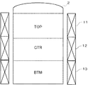
2 反応管
3 マニホールド
6 蓋体
9 ウエハボート
10 ヒータ部
11〜13 ヒータ
16〜18 電力コントローラ
21〜23 PH3ガス供給管
24〜26 流量調整部
50 制御部
51 モデル記憶部
52 レシピ記憶部
53 ROM
54 RAM
56 CPU
W 半導体ウエハ
Claims (7)
- 被処理体に形成された薄膜に不純物をドープするドープ処理および前記薄膜にドープされた不純物を拡散する拡散処理により被処理体に不純物ドープ薄膜を形成する熱処理システムであって、
前記ドープ処理および前記拡散処理に関する熱処理条件を記憶する熱処理条件記憶手段と、
前記熱処理条件記憶手段に記憶された前記ドープ処理に関する熱処理条件の変化と、前記ドープ処理における前記不純物ドープ薄膜の膜中不純物濃度の変化との関係を示すドープ処理モデルと、前記熱処理条件記憶手段に記憶された前記拡散処理に関する熱処理条件の変化と、前記拡散処理における前記不純物ドープ薄膜の膜中不純物濃度の変化との関係を示す拡散処理モデルと、を記憶するモデル記憶手段と、
前記熱処理条件記憶手段により記憶された熱処理条件で前記不純物ドープ薄膜を形成する熱処理手段と、
前記熱処理手段により形成された不純物ドープ薄膜の膜中不純物濃度が所望の範囲に含まれるか否かを判別し、前記所望の範囲に含まれないと判別すると、当該不純物ドープ薄膜の膜中不純物濃度と前記モデル記憶手段により記憶された前記ドープ処理モデル及び前記拡散処理モデルとに基づいて、前記膜中不純物濃度が所望の範囲に含まれるような前記ドープ処理および前記拡散処理の熱処理条件を算出する算出手段と、
前記熱処理条件記憶手段により記憶された熱処理条件を前記算出手段により算出された熱処理条件に変更し、変更した熱処理条件でドープ処理および拡散処理を行うことにより、前記所望の範囲に含まれる不純物ドープ薄膜の膜中不純物濃度に調整する調整手段と、
を、備えることを特徴とする熱処理システム。 - 複数枚の前記薄膜が形成された被処理体を収容する処理室内を加熱する加熱手段と、
前記処理室内にドープ用ガスを供給する複数のガス供給手段と、
前記処理室内の圧力を制御する圧力制御手段と、を、さらに備え、
前記モデル記憶手段に記憶された前記ドープ処理モデルは、前記ドープ処理における前記加熱手段により加熱される処理室内の温度、前記圧力制御手段により制御される処理室内の圧力、前記ガス供給手段により供給させるドープ用ガスの流量、および前記ドープ処理の時間の変化と、前記不純物ドープ薄膜の膜中不純物濃度の変化との関係を示すモデルであり、前記モデル記憶手段に記憶された前記拡散処理モデルは、前記拡散処理における前記加熱手段により加熱される処理室内の温度、および、前記拡散処理の時間の変化と、前記不純物ドープ薄膜の膜中不純物濃度の変化との関係を示すモデルであり、
前記算出手段は、前記膜中不純物濃度が所望の範囲に含まれるような前記ドープ処理における前記加熱手段により加熱される処理室内の温度、前記圧力制御手段により制御される処理室内の圧力、前記ガス供給手段により供給させるドープ用ガスの流量、前記ドープ処理の時間、前記拡散処理における前記加熱手段により加熱される処理室内の温度、および、前記拡散処理の時間を算出する、
ことを特徴とする請求項1に記載の熱処理システム。 - 前記処理室は複数のゾーンに区分けされ、
前記モデル記憶手段に記憶された前記ドープ処理モデルは、ゾーンごとの処理室内の温度およびドープ用ガスの流量の変化と、ゾーンごとの不純物ドープ薄膜の膜中不純物濃度の変化との関係を示し、前記モデル記憶手段に記憶された前記拡散処理モデルは、ゾーンごとの処理室内の温度の変化と、ゾーンごとの不純物ドープ薄膜の膜中不純物濃度の変化との関係を示し、
前記加熱手段は、前記処理室内のゾーンごとに温度設定可能であり、
前記ガス供給手段は、前記処理室内のゾーンごとにドープ用ガスの流量を設定可能である、ことを特徴とする請求項2に記載の熱処理システム。 - 前記モデル記憶手段に記憶された前記ドープ処理モデル及び前記拡散処理モデルは、前記薄膜の深さごとの膜中不純物濃度の変化と、前記熱処理条件の変化との関係を示すモデルが記憶されている、ことを特徴とする請求項1乃至3のいずれか1項に記載の熱処理システム。
- 前記算出手段は、前記膜中不純物濃度が、前記薄膜の深さ方向に均一となるように、前記ドープ処理および前記拡散処理の熱処理条件を算出する、ことを特徴とする請求項1乃至4のいずれか1項に記載の熱処理システム。
- 被処理体に形成された薄膜に不純物をドープするドープ処理および前記薄膜にドープされた不純物を拡散する拡散処理により被処理体に不純物ドープ薄膜を形成する熱処理方法であって、
前記ドープ処理および前記拡散処理に関する熱処理条件を記憶する熱処理条件記憶工程と、
前記熱処理条件記憶工程で記憶された前記ドープ処理に関する熱処理条件の変化と、前記ドープ処理における前記不純物ドープ薄膜の膜中不純物濃度の変化との関係を示すドープ処理モデルと、前記熱処理条件記憶工程で記憶された前記拡散処理に関する熱処理条件の変化と、前記拡散処理における前記不純物ドープ薄膜の膜中不純物濃度の変化との関係を示す拡散処理モデルと、を記憶するモデル記憶工程と、
前記熱処理条件記憶工程で記憶された熱処理条件で前記不純物ドープ薄膜を形成する熱処理工程と、
前記熱処理工程により形成された不純物ドープ薄膜の膜中不純物濃度が所望の範囲に含まれるか否かを判別し、前記所望の範囲に含まれないと判別すると、当該不純物ドープ薄膜の膜中不純物濃度と前記モデル記憶工程で記憶された前記ドープ処理モデル及び前記拡散処理モデルとに基づいて、前記膜中不純物濃度が所望の範囲に含まれるような前記ドープ処理および前記拡散処理の熱処理条件を算出する算出工程と、
前記熱処理条件記憶工程で記憶された熱処理条件を前記算出工程で算出された熱処理条件に変更し、変更した熱処理条件でドープ処理および拡散処理を行うことにより、前記所望の範囲に含まれる不純物ドープ薄膜の膜中不純物濃度に調整する調整工程と、
を、備えることを特徴とする熱処理方法。 - 被処理体に形成された薄膜に不純物をドープするドープ処理および前記薄膜にドープされた不純物を拡散する拡散処理により被処理体に不純物ドープ薄膜を形成する熱処理システムとして機能させるプログラムであって、
コンピュータを、
前記ドープ処理および前記拡散処理に関する熱処理条件を記憶する熱処理条件記憶手段、
前記熱処理条件記憶手段に記憶された前記ドープ処理に関する熱処理条件の変化と、前記ドープ処理における前記不純物ドープ薄膜の膜中不純物濃度の変化との関係を示すドープ処理モデルと、前記熱処理条件記憶工程で記憶された前記拡散処理に関する熱処理条件の変化と、前記拡散処理における前記不純物ドープ薄膜の膜中不純物濃度の変化との関係を示す拡散処理モデルと、を記憶するモデル記憶手段、
前記熱処理条件記憶手段により記憶された熱処理条件で前記不純物ドープ薄膜を形成する熱処理手段、
前記熱処理手段により形成された不純物ドープ薄膜の膜中不純物濃度が所望の範囲に含まれるか否かを判別し、前記所望の範囲に含まれないと判別すると、当該不純物ドープ薄膜の膜中不純物濃度と前記モデル記憶手段により記憶された前記ドープ処理モデル及び前記拡散処理モデルとに基づいて、前記膜中不純物濃度が所望の範囲に含まれるような前記ドープ処理および前記拡散処理の熱処理条件を算出する算出手段、
前記熱処理条件記憶手段により記憶された熱処理条件を前記算出手段により算出された熱処理条件に変更し、変更した熱処理条件でドープ処理および拡散処理を行うことにより、前記所望の範囲に含まれる不純物ドープ薄膜の膜中不純物濃度に調整する調整手段、
として機能させることを特徴とするプログラム。
Priority Applications (2)
| Application Number | Priority Date | Filing Date | Title |
|---|---|---|---|
| JP2015218054A JP6564689B2 (ja) | 2015-11-06 | 2015-11-06 | 熱処理システム、熱処理方法、及び、プログラム |
| US15/342,242 US9799577B2 (en) | 2015-11-06 | 2016-11-03 | Heat treatment system, heat treatment method, and program |
Applications Claiming Priority (1)
| Application Number | Priority Date | Filing Date | Title |
|---|---|---|---|
| JP2015218054A JP6564689B2 (ja) | 2015-11-06 | 2015-11-06 | 熱処理システム、熱処理方法、及び、プログラム |
Publications (2)
| Publication Number | Publication Date |
|---|---|
| JP2017092159A JP2017092159A (ja) | 2017-05-25 |
| JP6564689B2 true JP6564689B2 (ja) | 2019-08-21 |
Family
ID=58668180
Family Applications (1)
| Application Number | Title | Priority Date | Filing Date |
|---|---|---|---|
| JP2015218054A Active JP6564689B2 (ja) | 2015-11-06 | 2015-11-06 | 熱処理システム、熱処理方法、及び、プログラム |
Country Status (2)
| Country | Link |
|---|---|
| US (1) | US9799577B2 (ja) |
| JP (1) | JP6564689B2 (ja) |
Families Citing this family (1)
| Publication number | Priority date | Publication date | Assignee | Title |
|---|---|---|---|---|
| JP6999410B2 (ja) * | 2017-12-25 | 2022-01-18 | 東京エレクトロン株式会社 | 基板処理方法 |
Family Cites Families (6)
| Publication number | Priority date | Publication date | Assignee | Title |
|---|---|---|---|---|
| JP3130906B2 (ja) * | 1989-12-01 | 2001-01-31 | セイコーインスツルメンツ株式会社 | 半導体内壁に対する不純物の注入方法 |
| JPH04333239A (ja) * | 1991-05-08 | 1992-11-20 | Seiko Instr Inc | 不純物拡散領域の形成方法 |
| JPH11121389A (ja) * | 1997-10-13 | 1999-04-30 | Nec Kyushu Ltd | 縦型拡散炉および拡散方法 |
| JP4464979B2 (ja) * | 2007-03-05 | 2010-05-19 | 東京エレクトロン株式会社 | 処理システム、処理方法、及び、プログラム |
| JP5766647B2 (ja) * | 2012-03-28 | 2015-08-19 | 東京エレクトロン株式会社 | 熱処理システム、熱処理方法、及び、プログラム |
| JP5774532B2 (ja) | 2012-03-28 | 2015-09-09 | 東京エレクトロン株式会社 | 連続処理システム、連続処理方法、及び、プログラム |
-
2015
- 2015-11-06 JP JP2015218054A patent/JP6564689B2/ja active Active
-
2016
- 2016-11-03 US US15/342,242 patent/US9799577B2/en active Active
Also Published As
| Publication number | Publication date |
|---|---|
| US9799577B2 (en) | 2017-10-24 |
| JP2017092159A (ja) | 2017-05-25 |
| US20170133285A1 (en) | 2017-05-11 |
Similar Documents
| Publication | Publication Date | Title |
|---|---|---|
| JP5766647B2 (ja) | 熱処理システム、熱処理方法、及び、プログラム | |
| JP5788355B2 (ja) | 熱処理システム、熱処理方法、及び、プログラム | |
| US8664013B2 (en) | Continuous processing system, continuous processing method, and program | |
| JP5049303B2 (ja) | 熱処理装置、熱処理装置の温度調整方法、及び、プログラム | |
| US9798317B2 (en) | Substrate processing method and control apparatus | |
| JP6066847B2 (ja) | 基板処理方法及び制御装置 | |
| US10096499B2 (en) | Substrate processing method, program, control apparatus, film forming apparatus, and substrate processing system | |
| KR101149170B1 (ko) | 열처리 장치, 열처리 장치의 온도 조정 방법, 및 컴퓨터 프로그램을 기록한 기록 매체 | |
| US10395934B2 (en) | Control device, substrate processing system, substrate processing method, and program | |
| JP6512860B2 (ja) | 熱処理システム、熱処理方法、及び、プログラム | |
| JP6596316B2 (ja) | 熱処理システム、熱処理方法、及び、プログラム | |
| JP5049302B2 (ja) | 熱処理装置、熱処理装置の温度調整方法、及び、プログラム | |
| KR101689925B1 (ko) | 실리콘막의 형성 방법 및 그 형성 장치 | |
| JP2013207255A (ja) | 熱処理システム、熱処理方法、及び、プログラム | |
| JP6353802B2 (ja) | 処理システム、処理方法、及び、プログラム | |
| JP6564689B2 (ja) | 熱処理システム、熱処理方法、及び、プログラム | |
| JP6267881B2 (ja) | 基板処理方法及び制御装置 | |
| JP6378639B2 (ja) | 処理システム、処理方法、及び、プログラム | |
| JP6335128B2 (ja) | 熱処理システム、熱処理方法、及び、プログラム |
Legal Events
| Date | Code | Title | Description |
|---|---|---|---|
| A621 | Written request for application examination |
Free format text: JAPANESE INTERMEDIATE CODE: A621 Effective date: 20180413 |
|
| A977 | Report on retrieval |
Free format text: JAPANESE INTERMEDIATE CODE: A971007 Effective date: 20181113 |
|
| A131 | Notification of reasons for refusal |
Free format text: JAPANESE INTERMEDIATE CODE: A131 Effective date: 20190108 |
|
| A521 | Request for written amendment filed |
Free format text: JAPANESE INTERMEDIATE CODE: A523 Effective date: 20190308 |
|
| TRDD | Decision of grant or rejection written | ||
| A01 | Written decision to grant a patent or to grant a registration (utility model) |
Free format text: JAPANESE INTERMEDIATE CODE: A01 Effective date: 20190702 |
|
| A61 | First payment of annual fees (during grant procedure) |
Free format text: JAPANESE INTERMEDIATE CODE: A61 Effective date: 20190729 |
|
| R150 | Certificate of patent or registration of utility model |
Ref document number: 6564689 Country of ref document: JP Free format text: JAPANESE INTERMEDIATE CODE: R150 |
|
| R250 | Receipt of annual fees |
Free format text: JAPANESE INTERMEDIATE CODE: R250 |
|
| R250 | Receipt of annual fees |
Free format text: JAPANESE INTERMEDIATE CODE: R250 |