EP0421395B2 - Anordnung zur Umwandlung einer elektrischen Eingangsgrösse in ein dazu proportionales elektrisches Gleichsignal - Google Patents
Anordnung zur Umwandlung einer elektrischen Eingangsgrösse in ein dazu proportionales elektrisches Gleichsignal Download PDFInfo
- Publication number
- EP0421395B2 EP0421395B2 EP90118995A EP90118995A EP0421395B2 EP 0421395 B2 EP0421395 B2 EP 0421395B2 EP 90118995 A EP90118995 A EP 90118995A EP 90118995 A EP90118995 A EP 90118995A EP 0421395 B2 EP0421395 B2 EP 0421395B2
- Authority
- EP
- European Patent Office
- Prior art keywords
- pulse
- pulse duration
- quantization
- signal
- value
- Prior art date
- Legal status (The legal status is an assumption and is not a legal conclusion. Google has not performed a legal analysis and makes no representation as to the accuracy of the status listed.)
- Expired - Lifetime
Links
Images


Classifications
-
- H—ELECTRICITY
- H03—ELECTRONIC CIRCUITRY
- H03M—CODING; DECODING; CODE CONVERSION IN GENERAL
- H03M1/00—Analogue/digital conversion; Digital/analogue conversion
- H03M1/66—Digital/analogue converters
- H03M1/68—Digital/analogue converters with conversions of different sensitivity, i.e. one conversion relating to the more significant digital bits and another conversion to the less significant bits
-
- H—ELECTRICITY
- H03—ELECTRONIC CIRCUITRY
- H03M—CODING; DECODING; CODE CONVERSION IN GENERAL
- H03M1/00—Analogue/digital conversion; Digital/analogue conversion
- H03M1/66—Digital/analogue converters
- H03M1/82—Digital/analogue converters with intermediate conversion to time interval
- H03M1/822—Digital/analogue converters with intermediate conversion to time interval using pulse width modulation
Definitions
- the invention relates to an arrangement for converting a electrical input variable into a proportional electrical DC signal, with a first digital pulse duration modulator limited resolution, which is a first periodic Pulse train delivers that with that of the limited resolution corresponding quantization value of the input variable under Neglect of the quantization remainder modulated with pulse duration is a second pulse duration module of limited resolution, which provides a second periodic pulse train, which in Dependence on the quantization remainder is pulse duration modulated, and with an averaging circuit for forming an average signal value from the pulse duration modulated pulse trains.
- a first digital pulse duration modulator limited resolution which is a first periodic Pulse train delivers that with that of the limited resolution corresponding quantization value of the input variable under Neglect of the quantization remainder modulated with pulse duration is a second pulse duration module of limited resolution, which provides a second periodic pulse train, which in Dependence on the quantization remainder is pulse duration modulated, and with an averaging circuit for forming an average signal value from the pulse duration modulated pulse trains.
- Such an arrangement is e.g. B. is known from US-A-3 823 396.
- EP-A-0 280 321 describes an arrangement for converting a digital electrical variable into a proportional signal proportional to it, in which the digital input variable represented by m + n bits likewise has a resolution corresponding to a limited resolution and consists of the m higher-order bits Quantization value and a quantization residue consisting of the n least significant bits is divided.
- pulse duration modulation is not used, but the quantization value and the quantization residue are supplied to two separate digital-to-analog converters, which are constructed in a conventional manner with resistance networks.
- One digital-to-analog converter supplies a direct current that corresponds to the quantization value
- the other digital-to-analog converter supplies a direct current that corresponds to the quantization residue multiplied by a factor of 2 n .
- the two direct currents are summed by an analog adder which is weighted in such a way that the overweighting of the quantization residue is compensated for.
- a correction value is added to the quantization residue before its digital-to-analog conversion, which depends on the quantization value.
- the various correction values are stored, for example, in a read-only memory from which they are read out with addressing by the quantization value.
- the object of the invention is to provide an arrangement of the initially specified type, in which the by an analog Difficulties arising from signal processing avoided are.
- this object is achieved in that the second supplied by the second pulse duration modulator periodic pulse train with the sum of that of the limited Resolution corresponding quantization value and with a quantization residue multiplied by a predetermined factor is pulse width modulated, and that a switching arrangement is provided which the pulses of the two pulse sequences turns through to the averaging circuit that the ratio of the switched pulses of the second Pulse train for the total number of switched pulses is equal to the reciprocal of the predetermined factor.
- the sum formation takes place with compensation the overweighting of the quantization residue Counting and alternating switching of impulses, so with purely digital means.
- the result is a new one Pulse train, whose DC signal mean of the total electrical Input variable including the quantization residue is proportional. From the new pulse train by the averaging circuit in the same way as in one supplied by a single pulse duration modulator Pulse train of the DC signal mean are formed without that here a different weighting through resistors or other similar means must be done.
- Fig. 1 shows schematically the known principle of converting an electrical used in the invention
- Input variable E in an analog output signal A which is proportional to the input variable electrical DC signal is formed.
- a "direct signal” here is a direct current or a direct voltage to understand.
- the input variable E is fed as a modulation signal to a pulse duration modulator 10, which emits a pulse train I at the output, the pulses of which follow one another with a constant period and one Duration that is proportional to the value of the input variable E.
- the duty cycle is also the Pulses, i.e. the ratio of the pulse duration to the period, proportional to the value of the input variable E.
- the repetition frequency of the pulse train I is, for example, by a clock signal supplied by a clock generator 12 certainly.
- the pulse duration modulated pulse sequence 1 is fed to an averaging circuit 14, which is on Output emits a signal that the DC signal average, that is, the DC average or the DC voltage average corresponds to the pulse duration modulated pulses.
- the averaging circuit 14 can, for example be formed by a low-pass filter.
- the average signal value obtained from the averaging circuit 14 is proportional to the duty cycle of the pulse duration modulated pulse train I, and since this Duty cycle is proportional to the value of the input variable E, the mean signal value is also the value proportional to the input variable E.
- the DC mean value thus represents the desired output signal A. represents.
- Fig. 2 shows a conversion circuit which maintains the principle of a limited resolution performed pulse duration modulation results in a conversion with much higher accuracy.
- the input variable E is an analog variable.
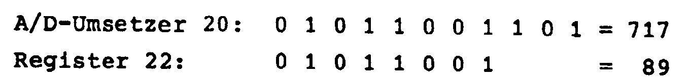
- the analog input variable E is fed to an analog-to-digital converter 20 with the relatively high resolution of 11 bits.
- the analog-to-digital converter 20 outputs an eleven-digit binary code group at eleven outputs, which reproduces the quantized value of the analog input variable as a binary number.
- the lowest output of the analog-to-digital converter 20 is assigned to the dual position with the lowest place value and the top output of the dual place with the highest place value.
- the eight outputs of the highest place values are connected to the inputs of an eight-stage register 22, into which a binary code group is thus entered, which consists of the eight binary digits of the highest place value of the binary code group supplied by the analog-to-digital converter 20.
- the outputs of the register 22 are connected to the modulation signal inputs of a digital pulse duration modulator 24, which has the same 8-bit resolution as the register 22.
- the pulse duration modulator 24 corresponds to the pulse duration modulator 10 of FIG. 1 and outputs at the output a pulse duration modulated pulse train I 1 , the pulse period of which is determined by a clock signal supplied by a clock generator 26 and the pulses of which have a duration which is proportional to the digital numerical value in the register 22 is.
- the output of the pulse duration modulator 24 is connected to the signal input of a gate circuit 28, the control input of which is connected to the output of a control circuit 30 synchronized by the clock generator 26, so that the gate circuit 28 is opened or closed by a control signal S supplied by the control circuit 30.
- the output of the gate circuit 28 is connected via an OR circuit 32 to an averaging circuit 34, which corresponds to the averaging circuit 14 of FIG. 1 and can be formed, for example, by a low-pass filter.
- an averaging circuit 34 which corresponds to the averaging circuit 14 of FIG. 1 and can be formed, for example, by a low-pass filter.
- a second eight-stage register 36 is provided, the three inputs of which are assigned the lowest value with the three outputs of the analog-digital converter 20 assigned to the lowest value are connected while the other inputs of register 36 are not connected.
- Register 36 says hence an eight-digit binary number, the first five digits of which have the value "0" and the last three digits the binary digits of the last three digits of the eleven-digit dual number are those from the analog-to-digital converter 20 is issued.
- the outputs of the register 36 are with an assigned group of inputs of an adder 38 connected, the second input group of which is connected to the outputs of the register 22.
- the adder 38 forms the sum of the two eight-digit dual numbers that are in registers 22 and 36, and gives one this sum corresponds to the eight-digit dual number at its outputs.
- the outputs of the adder 38 are connected to the modulation signal inputs of a digital pulse duration modulator 40, which is of the same type as the pulse duration modulator 24, that is to say has the same limited resolution of 8 bits.
- the pulse duration modulator 40 also receives the clock signal supplied by the clock generator 26 and emits a pulse duration modulated pulse sequence I 2 at the output, the pulses of which have the same constant period as determined by the clock generator 26 as the pulses of the pulse sequence I 1 and the duration of which corresponds to the numerical value of the adder 38 given dual number is proportional.
- the output of the pulse duration modulator 40 is connected to the signal input of a gate circuit 42, which receives at its control input the control signal S supplied by the control circuit 30 via an inverter 44 so that the gate circuit 42 is opened and closed in the opposite direction to the gate circuit 28.
- the output of the gate circuit 42 is connected to the averaging circuit 34 via the OR circuit 32.
- the binary digits of the last three digits of the binary number in the register 36 are added with the same digits as the binary digits of the last three digits of the dual number in the register 22.
- the addition follows the following scheme:
- the dual number in register 22 corresponds to a quantization value of input variable E with the resolution limited to 8 bits, the quantization remainder being disregarded.
- the quantization residue is only zero if the value of the input variable E happens to correspond exactly to the quantization value. If the quantization residue is different from zero, the pulse duration of the pulse duration-modulated pulse train I 1 is smaller by an amount proportional to the quantization residue than the pulse duration, which would correspond to the exact value of the input variable E.
- the dual number output by the adder 38 corresponds to the sum of the quantization value taken into account in the pulse duration modulator 24 and the quantization residue multiplied by a factor of 8, this sum also being represented with a resolution of 8 bits. If the quantization residue is different from zero, the pulse duration of the pulse duration-modulated pulse train I 2 is 7 times greater than the quantization residue than the pulse duration, which would correspond to the exact value of the input variable E.
- pulse sequences I 1 and I 2 are shown in the diagrams from FIG. 3 provided with the same designations. 3 show the time profile of the control signal S supplied by the control circuit 30 and the total pulse sequence I G obtained at the output of the OR circuit 32.
- control signal S When the control signal S has the high signal level, the gate circuit 28 is open and the gate circuit 42 closed. When the control signal S has the low signal level, the gate circuit 42 is open and the gate circuit 28 closed.
- the control circuit 30 is designed such that the control signal S has the high signal level for seven consecutive pulse periods of the pulse trains I 1 and I 2 and then the low signal level for one pulse period.
- the total pulse train I G transmitted to the averaging circuit 34 thus contains seven pulses of the pulse train I 1 and one pulse of the pulse train I 2 in eight successive pulses.
- the average signal value formed by the averaging circuit 34 is proportional to this average pulse duration D M.
- the term D 8R / 8 corresponds to a portion of the pulse duration proportional to the simple quantization residue.
- the measures described above for increasing the accuracy therefore exist in the general case in that for the pulse duration modulation of the second pulse sequence the sum of that for the modulation of the first pulse sequence used quantization value and from the quantization residue multiplied by a factor n is used and that the pulse sequence used for averaging is made up of pulses of two pulse sequences is composed that n consecutive pulses each a pulse of the second Pulse train and (n-1) pulses of the first pulse train included. Then the pulse in the second pulse train additionally contained n-fold quantization residue on average divided into n pulse periods.
- the ratio of the number of Pulses of the second pulse sequence for the total number of pulses correspond to the reciprocal of the factor with which the quantization residue is multiplied.
- the measures described can be carried out with little additional circuitry the use of 8 bit circuits limits a significant increase in the accuracy of the conversion an input variable into a proportional signal proportional to it, which corresponds to the 8 bit resolution Accuracy can be achieved.
- the solution described proves to be particularly useful advantageous because integrated circuits are commercially available which contain two 8-bit permanent modulators. It is therefore possible to use the second pulse duration modulator to increase the accuracy.
- the invention is not limited to the case where the input variable is available as an analog signal, as taken as an example in the above description.
- the input variable can by any electrical signal can be represented, for example by a digital signal, a frequency or similar. If, for example, the input variable is represented by a parallel binary code group 2 can be replaced by a register in which the code group is stored, or the parallel transmission lines over which the code group is transmitted can be connected directly to the inputs of registers 22 and 36.
- the changes required in any case the circuit is familiar to the person skilled in the art.
Landscapes
- Engineering & Computer Science (AREA)
- Theoretical Computer Science (AREA)
- Analogue/Digital Conversion (AREA)
Description
- Fig. 1
- das Prinzipschema der bei der Erfindung angewendeten Umwandlung einer Eingangsgröße in ein dazu proportionales Gleichsignal durch digitale Pulsdauermodulation,
- Fig. 2
- das Blockschaltbild einer Ausführungsform der erfindungsgemäßen Anordnung und
- Fig. 3
- Diagramme von Signalen, die in der Anordnuna von Fig. 2 auftreten.

Claims (1)
- Anordnung zur Umwandlung einer elektrischen Eingangsgröße (E) in ein dazu proportionales elektrisches Gleichsignal (A), mit einem ersten digitalen Pulsdauermodulator (24) begrenzter Auflösung, der eine erste periodische Impulsfolge (I1) liefert, die mit dem der begrenzten Auflösung entsprechenden Quantisierungswert der Eingangsgröße unter Vernachlässigung des Quantisierungsrestes pulsdauermoduliert ist, einem zweiten Pulsdauermodulator (40) begrenzter Auflösung, der eine zweite periodische Impulsfolge (I2) liefert, die in Abhängigkeit vom Quantisierungsrest pulsdauermoduliert ist, und mit einer Mittelungsschaltung (34) zur Bildung eines Gleichsignalmittelwerts aus den pulsdauermodulierten Impulsfolgen, dadurch gekennzeichnet, daß die von dem zweiten Pulsdauermodulator (40) gelieferte zweite periodische Impulsfolge mit der Summe aus dem der begrenzten Auflösung entsprechenden Quantisierungswert und dem mit einem vorbestimmten Faktor multiplizierten Quantisierungsrest pulsdauermoduliert ist, und daß eine Umschaltanordnung (28, 30, 42, 44) vorgesehen ist, die die Impulse der beiden Impulsfolgen derart abwechselnd zur Mittelungsschaltung (34) durchschaltet, daß das Verhältnis der Anzahl der durchgeschalteten Impulse der zweiten Impulsfolge (I2) zur Gesamtzahl der durchgeschalteten Impulse gleich dem Kehrwert des vorbestimmten Faktors ist.
Applications Claiming Priority (2)
| Application Number | Priority Date | Filing Date | Title |
|---|---|---|---|
| DE3933491 | 1989-10-06 | ||
| DE3933491A DE3933491A1 (de) | 1989-10-06 | 1989-10-06 | Anordnung zur umwandlung einer elektrischen eingangsgroesse in ein dazu proportionales elektrisches gleichsignal |
Publications (4)
| Publication Number | Publication Date |
|---|---|
| EP0421395A2 EP0421395A2 (de) | 1991-04-10 |
| EP0421395A3 EP0421395A3 (en) | 1993-04-21 |
| EP0421395B1 EP0421395B1 (de) | 1995-12-20 |
| EP0421395B2 true EP0421395B2 (de) | 1998-11-11 |
Family
ID=6391003
Family Applications (1)
| Application Number | Title | Priority Date | Filing Date |
|---|---|---|---|
| EP90118995A Expired - Lifetime EP0421395B2 (de) | 1989-10-06 | 1990-10-04 | Anordnung zur Umwandlung einer elektrischen Eingangsgrösse in ein dazu proportionales elektrisches Gleichsignal |
Country Status (5)
| Country | Link |
|---|---|
| US (1) | US5103462A (de) |
| EP (1) | EP0421395B2 (de) |
| JP (1) | JPH0783267B2 (de) |
| DE (2) | DE3933491A1 (de) |
| FI (1) | FI99179C (de) |
Families Citing this family (14)
| Publication number | Priority date | Publication date | Assignee | Title |
|---|---|---|---|---|
| JP2777291B2 (ja) * | 1991-04-30 | 1998-07-16 | 株式会社東芝 | アナログ・ディジタル混在集積回路 |
| FR2682768A1 (fr) * | 1991-10-21 | 1993-04-23 | Otic Fischer & Porter | Methodes de conversion de rapports d'impedances applicables aux appareils de mesure, notamment aux transmetteurs de pression industriels, et leurs dispositifs de mise en óoeuvre. |
| US5471505A (en) * | 1993-10-01 | 1995-11-28 | Elsag International N.V. | Method and apparatus for increasing the resolution of a digital to analog converted pulse width modulated signal |
| EP0892500B1 (de) | 1997-07-17 | 2003-02-26 | STMicroelectronics S.r.l. | System zur Auflösungserhöhung bei der Umwandlung von digitalen Daten in PWM-Signale zur Steuerung einer Vollbrückenausgangsstufe |
| JP3601315B2 (ja) * | 1997-11-05 | 2004-12-15 | セイコーエプソン株式会社 | ステップモータの制御装置、制御方法および計時装置 |
| US5959501A (en) * | 1998-01-14 | 1999-09-28 | Harris Corporation | Class D amplifier with scaled clock and related methods |
| JP2900153B1 (ja) * | 1998-02-10 | 1999-06-02 | セイコーインスツルメンツ株式会社 | アナログ電子時計 |
| AT409731B (de) * | 1998-10-16 | 2002-10-25 | Fronius Schweissmasch Prod | Regelvorrichtung für ein schweissgerät |
| WO2001071914A1 (en) * | 2000-03-23 | 2001-09-27 | Marconi Communications Limited | Method and apparatus for generating a pulse width modulated signal and optical attenuator controlled by a pulse width modulated signal |
| JP4260478B2 (ja) * | 2000-10-25 | 2009-04-30 | コーニンクレッカ フィリップス エレクトロニクス エヌ ヴィ | 回路装置 |
| US6714770B2 (en) * | 2001-11-16 | 2004-03-30 | Aleksander Maksimov | Method and apparatus for prevention of the concurrence of modes condition during operation of electronic device |
| CN1310427C (zh) * | 2004-02-25 | 2007-04-11 | 凌阳科技股份有限公司 | 脉波宽度调变电路与方法 |
| US8902089B2 (en) * | 2012-05-02 | 2014-12-02 | Qualcomm Incorporated | Systems and methods for performing digital modulation |
| FR2999836B1 (fr) * | 2012-12-18 | 2018-11-09 | Safran Electronics & Defense | Procede de conversion numerique analogique a modulation de largeur d'implulsion optimise |
Family Cites Families (15)
| Publication number | Priority date | Publication date | Assignee | Title |
|---|---|---|---|---|
| US4112368A (en) * | 1970-07-13 | 1978-09-05 | Westinghouse Electric Corp. | Constant amplitude carrier communications system |
| JPS5149531B2 (de) * | 1971-11-13 | 1976-12-27 | ||
| US3823396A (en) * | 1972-04-17 | 1974-07-09 | Electronics Processors Inc | Digital to analog converter incorporating multiple time division switching circuits |
| GB1553697A (en) * | 1975-07-17 | 1979-10-03 | Licentia Gmbh | Digital to analogue converter arrangements |
| JPS5228205A (en) * | 1975-08-28 | 1977-03-03 | Sony Corp | Station selector unit |
| DE2721993C3 (de) * | 1977-05-14 | 1980-09-18 | Licentia Patent-Verwaltungs-Gmbh, 6000 Frankfurt | Schaltungsanordnung zum Übertragen von digitalen Gleichstromsignalen mittels Trägerschwingungen vorgegebener Frequenz |
| US4334237A (en) * | 1980-02-07 | 1982-06-08 | Rca Corporation | Adaptive amplitude averaging for weighting quantizing noise |
| JPS57155833A (en) * | 1981-03-23 | 1982-09-27 | Toshiba Corp | Digital-to-analog converting circuit |
| JPS5847325A (ja) * | 1981-09-17 | 1983-03-19 | Sanyo Electric Co Ltd | パルス幅変調回路 |
| JPS5911026A (ja) * | 1982-07-12 | 1984-01-20 | Yokogawa Hokushin Electric Corp | デイジタル・アナログ変換器 |
| DE3306334A1 (de) * | 1983-02-23 | 1984-08-23 | Siemens AG, 1000 Berlin und 8000 München | Quantisierer fuer dpcm-codierer |
| GB2144005B (en) * | 1983-07-28 | 1986-10-22 | Rca Corp | Digital-to-analog converter useful in a television receiver |
| JPS6235709A (ja) * | 1985-08-09 | 1987-02-16 | Hitachi Ltd | デジタル回路 |
| US4685114A (en) * | 1986-02-27 | 1987-08-04 | The Charles Stark Draper Laboratory, Inc. | Waveform modulation system |
| JPS62231569A (ja) * | 1986-03-31 | 1987-10-12 | Fuji Photo Film Co Ltd | 予測誤差の量子化方法 |
-
1989
- 1989-10-06 DE DE3933491A patent/DE3933491A1/de active Granted
-
1990
- 1990-09-26 FI FI904733A patent/FI99179C/fi not_active IP Right Cessation
- 1990-10-02 US US07/591,696 patent/US5103462A/en not_active Expired - Fee Related
- 1990-10-04 DE DE59009979T patent/DE59009979D1/de not_active Expired - Fee Related
- 1990-10-04 EP EP90118995A patent/EP0421395B2/de not_active Expired - Lifetime
- 1990-10-05 JP JP2266592A patent/JPH0783267B2/ja not_active Expired - Lifetime
Also Published As
| Publication number | Publication date |
|---|---|
| DE3933491A1 (de) | 1991-04-18 |
| EP0421395A3 (en) | 1993-04-21 |
| FI99179B (fi) | 1997-06-30 |
| DE59009979D1 (de) | 1996-02-01 |
| FI904733A0 (fi) | 1990-09-26 |
| US5103462A (en) | 1992-04-07 |
| EP0421395B1 (de) | 1995-12-20 |
| FI99179C (fi) | 1997-10-10 |
| JPH03207124A (ja) | 1991-09-10 |
| JPH0783267B2 (ja) | 1995-09-06 |
| EP0421395A2 (de) | 1991-04-10 |
| DE3933491C2 (de) | 1991-10-17 |
Similar Documents
| Publication | Publication Date | Title |
|---|---|---|
| EP0421395B2 (de) | Anordnung zur Umwandlung einer elektrischen Eingangsgrösse in ein dazu proportionales elektrisches Gleichsignal | |
| DE3003099C2 (de) | Digital-Analog-Wandler mit Kompensationsschaltung | |
| DE3902313C2 (de) | Analog /Digitalwandler | |
| DE3587950T2 (de) | Paralleler algorithmischer Digital-/Analogwandler. | |
| DE3643161A1 (de) | Verfahren und vorrichtung zur offsetspannungs-korrektur in einem analog/digital-umsetzer | |
| DE3129338A1 (de) | Signalwandler | |
| DE3202789A1 (de) | Digital/analog-wandlerkreis | |
| DE2451983C2 (de) | Digital-Analogwandler | |
| DE2836079A1 (de) | Digital-analog-umsetzer | |
| DE2801272C2 (de) | Schaltungsanordnung zur Durchführung einer gewichtsfaktorabhängigen Ladungsaufteilung und -übertragung | |
| DE3408550C2 (de) | ||
| DE3237283A1 (de) | Analog/digital-wandler | |
| DE3147578C2 (de) | ||
| DE2724347C2 (de) | Deltamodulator mit einem quantisierenden Vergleicher | |
| DE3685836T2 (de) | Interpolativer da-wandler. | |
| DE69924013T2 (de) | Kapazitiver paralleler analog-digitalwandler | |
| DE69409547T2 (de) | Digital-analogwandler mit niedriger auflösung und hoher linearität ohne trim | |
| DE2900383C2 (de) | Interpolativer PCM-Dekodierer | |
| DE69521452T2 (de) | Schaltung zur Digital-/Analogumsetzung und die Schaltung benutzender A/D-Wandler | |
| DE2804915C2 (de) | ||
| DE2229398A1 (de) | Differentielles Puls-Code-Modulations-System mit periodischer Änderung des Modulator-Schrittes | |
| DE3046772C2 (de) | Taktgenerator | |
| EP0265637B1 (de) | Impulsformer | |
| DE69414538T2 (de) | Digital/Analogwandlerschaltung | |
| DE3124194A1 (de) | "frequenzabfuehlschaltung" |
Legal Events
| Date | Code | Title | Description |
|---|---|---|---|
| PUAI | Public reference made under article 153(3) epc to a published international application that has entered the european phase |
Free format text: ORIGINAL CODE: 0009012 |
|
| AK | Designated contracting states |
Kind code of ref document: A2 Designated state(s): CH DE FR GB IT LI |
|
| PUAL | Search report despatched |
Free format text: ORIGINAL CODE: 0009013 |
|
| AK | Designated contracting states |
Kind code of ref document: A3 Designated state(s): CH DE FR GB IT LI |
|
| 17P | Request for examination filed |
Effective date: 19930625 |
|
| 17Q | First examination report despatched |
Effective date: 19950531 |
|
| GRAA | (expected) grant |
Free format text: ORIGINAL CODE: 0009210 |
|
| ITF | It: translation for a ep patent filed | ||
| AK | Designated contracting states |
Kind code of ref document: B1 Designated state(s): CH DE FR GB IT LI |
|
| REF | Corresponds to: |
Ref document number: 59009979 Country of ref document: DE Date of ref document: 19960201 |
|
| REG | Reference to a national code |
Ref country code: CH Ref legal event code: NV Representative=s name: DIPL.-ING. VOLKER MORSTADT |
|
| ET | Fr: translation filed | ||
| GBT | Gb: translation of ep patent filed (gb section 77(6)(a)/1977) |
Effective date: 19960327 |
|
| PLBQ | Unpublished change to opponent data |
Free format text: ORIGINAL CODE: EPIDOS OPPO |
|
| PLBI | Opposition filed |
Free format text: ORIGINAL CODE: 0009260 |
|
| PLBF | Reply of patent proprietor to notice(s) of opposition |
Free format text: ORIGINAL CODE: EPIDOS OBSO |
|
| 26 | Opposition filed |
Opponent name: KROHNE MESSTECHNIK GMBH & CO. KG Effective date: 19960920 |
|
| PLBF | Reply of patent proprietor to notice(s) of opposition |
Free format text: ORIGINAL CODE: EPIDOS OBSO |
|
| PLBF | Reply of patent proprietor to notice(s) of opposition |
Free format text: ORIGINAL CODE: EPIDOS OBSO |
|
| PLAW | Interlocutory decision in opposition |
Free format text: ORIGINAL CODE: EPIDOS IDOP |
|
| PLAW | Interlocutory decision in opposition |
Free format text: ORIGINAL CODE: EPIDOS IDOP |
|
| PUAH | Patent maintained in amended form |
Free format text: ORIGINAL CODE: 0009272 |
|
| STAA | Information on the status of an ep patent application or granted ep patent |
Free format text: STATUS: PATENT MAINTAINED AS AMENDED |
|
| 27A | Patent maintained in amended form |
Effective date: 19981111 |
|
| AK | Designated contracting states |
Kind code of ref document: B2 Designated state(s): CH DE FR GB IT LI |
|
| REG | Reference to a national code |
Ref country code: CH Ref legal event code: AEN Free format text: AUFRECHTERHALTUNG DES PATENTES IN GEAENDERTER FORM |
|
| GBTA | Gb: translation of amended ep patent filed (gb section 77(6)(b)/1977) | ||
| ET3 | Fr: translation filed ** decision concerning opposition | ||
| PGFP | Annual fee paid to national office [announced via postgrant information from national office to epo] |
Ref country code: CH Payment date: 19990915 Year of fee payment: 10 |
|
| PGFP | Annual fee paid to national office [announced via postgrant information from national office to epo] |
Ref country code: DE Payment date: 20001005 Year of fee payment: 11 |
|
| PGFP | Annual fee paid to national office [announced via postgrant information from national office to epo] |
Ref country code: FR Payment date: 20001012 Year of fee payment: 11 |
|
| PG25 | Lapsed in a contracting state [announced via postgrant information from national office to epo] |
Ref country code: LI Free format text: LAPSE BECAUSE OF NON-PAYMENT OF DUE FEES Effective date: 20001031 Ref country code: CH Free format text: LAPSE BECAUSE OF NON-PAYMENT OF DUE FEES Effective date: 20001031 |
|
| REG | Reference to a national code |
Ref country code: CH Ref legal event code: PL |
|
| PGFP | Annual fee paid to national office [announced via postgrant information from national office to epo] |
Ref country code: GB Payment date: 20010914 Year of fee payment: 12 |
|
| REG | Reference to a national code |
Ref country code: GB Ref legal event code: IF02 |
|
| PG25 | Lapsed in a contracting state [announced via postgrant information from national office to epo] |
Ref country code: FR Free format text: LAPSE BECAUSE OF NON-PAYMENT OF DUE FEES Effective date: 20020628 |
|
| PG25 | Lapsed in a contracting state [announced via postgrant information from national office to epo] |
Ref country code: DE Free format text: LAPSE BECAUSE OF NON-PAYMENT OF DUE FEES Effective date: 20020702 |
|
| REG | Reference to a national code |
Ref country code: FR Ref legal event code: ST |
|
| PG25 | Lapsed in a contracting state [announced via postgrant information from national office to epo] |
Ref country code: GB Free format text: LAPSE BECAUSE OF NON-PAYMENT OF DUE FEES Effective date: 20021004 |
|
| GBPC | Gb: european patent ceased through non-payment of renewal fee |
Effective date: 20021004 |
|
| PG25 | Lapsed in a contracting state [announced via postgrant information from national office to epo] |
Ref country code: IT Free format text: LAPSE BECAUSE OF NON-PAYMENT OF DUE FEES;WARNING: LAPSES OF ITALIAN PATENTS WITH EFFECTIVE DATE BEFORE 2007 MAY HAVE OCCURRED AT ANY TIME BEFORE 2007. THE CORRECT EFFECTIVE DATE MAY BE DIFFERENT FROM THE ONE RECORDED. Effective date: 20051004 |
|
| PLAB | Opposition data, opponent's data or that of the opponent's representative modified |
Free format text: ORIGINAL CODE: 0009299OPPO |