EP0421395B2 - Arrangement for the conversion of an electrical input value to a direct electrical signal proportional thereto - Google Patents
Arrangement for the conversion of an electrical input value to a direct electrical signal proportional thereto Download PDFInfo
- Publication number
- EP0421395B2 EP0421395B2 EP90118995A EP90118995A EP0421395B2 EP 0421395 B2 EP0421395 B2 EP 0421395B2 EP 90118995 A EP90118995 A EP 90118995A EP 90118995 A EP90118995 A EP 90118995A EP 0421395 B2 EP0421395 B2 EP 0421395B2
- Authority
- EP
- European Patent Office
- Prior art keywords
- pulse
- pulse duration
- quantization
- signal
- value
- Prior art date
- Legal status (The legal status is an assumption and is not a legal conclusion. Google has not performed a legal analysis and makes no representation as to the accuracy of the status listed.)
- Expired - Lifetime
Links
Images


Classifications
-
- H—ELECTRICITY
- H03—ELECTRONIC CIRCUITRY
- H03M—CODING; DECODING; CODE CONVERSION IN GENERAL
- H03M1/00—Analogue/digital conversion; Digital/analogue conversion
- H03M1/66—Digital/analogue converters
- H03M1/68—Digital/analogue converters with conversions of different sensitivity, i.e. one conversion relating to the more significant digital bits and another conversion to the less significant bits
-
- H—ELECTRICITY
- H03—ELECTRONIC CIRCUITRY
- H03M—CODING; DECODING; CODE CONVERSION IN GENERAL
- H03M1/00—Analogue/digital conversion; Digital/analogue conversion
- H03M1/66—Digital/analogue converters
- H03M1/82—Digital/analogue converters with intermediate conversion to time interval
- H03M1/822—Digital/analogue converters with intermediate conversion to time interval using pulse width modulation
Definitions
- the invention relates to an arrangement for converting a electrical input variable into a proportional electrical DC signal, with a first digital pulse duration modulator limited resolution, which is a first periodic Pulse train delivers that with that of the limited resolution corresponding quantization value of the input variable under Neglect of the quantization remainder modulated with pulse duration is a second pulse duration module of limited resolution, which provides a second periodic pulse train, which in Dependence on the quantization remainder is pulse duration modulated, and with an averaging circuit for forming an average signal value from the pulse duration modulated pulse trains.
- a first digital pulse duration modulator limited resolution which is a first periodic Pulse train delivers that with that of the limited resolution corresponding quantization value of the input variable under Neglect of the quantization remainder modulated with pulse duration is a second pulse duration module of limited resolution, which provides a second periodic pulse train, which in Dependence on the quantization remainder is pulse duration modulated, and with an averaging circuit for forming an average signal value from the pulse duration modulated pulse trains.
- Such an arrangement is e.g. B. is known from US-A-3 823 396.
- EP-A-0 280 321 describes an arrangement for converting a digital electrical variable into a proportional signal proportional to it, in which the digital input variable represented by m + n bits likewise has a resolution corresponding to a limited resolution and consists of the m higher-order bits Quantization value and a quantization residue consisting of the n least significant bits is divided.
- pulse duration modulation is not used, but the quantization value and the quantization residue are supplied to two separate digital-to-analog converters, which are constructed in a conventional manner with resistance networks.
- One digital-to-analog converter supplies a direct current that corresponds to the quantization value
- the other digital-to-analog converter supplies a direct current that corresponds to the quantization residue multiplied by a factor of 2 n .
- the two direct currents are summed by an analog adder which is weighted in such a way that the overweighting of the quantization residue is compensated for.
- a correction value is added to the quantization residue before its digital-to-analog conversion, which depends on the quantization value.
- the various correction values are stored, for example, in a read-only memory from which they are read out with addressing by the quantization value.
- the object of the invention is to provide an arrangement of the initially specified type, in which the by an analog Difficulties arising from signal processing avoided are.
- this object is achieved in that the second supplied by the second pulse duration modulator periodic pulse train with the sum of that of the limited Resolution corresponding quantization value and with a quantization residue multiplied by a predetermined factor is pulse width modulated, and that a switching arrangement is provided which the pulses of the two pulse sequences turns through to the averaging circuit that the ratio of the switched pulses of the second Pulse train for the total number of switched pulses is equal to the reciprocal of the predetermined factor.
- the sum formation takes place with compensation the overweighting of the quantization residue Counting and alternating switching of impulses, so with purely digital means.
- the result is a new one Pulse train, whose DC signal mean of the total electrical Input variable including the quantization residue is proportional. From the new pulse train by the averaging circuit in the same way as in one supplied by a single pulse duration modulator Pulse train of the DC signal mean are formed without that here a different weighting through resistors or other similar means must be done.
- Fig. 1 shows schematically the known principle of converting an electrical used in the invention
- Input variable E in an analog output signal A which is proportional to the input variable electrical DC signal is formed.
- a "direct signal” here is a direct current or a direct voltage to understand.
- the input variable E is fed as a modulation signal to a pulse duration modulator 10, which emits a pulse train I at the output, the pulses of which follow one another with a constant period and one Duration that is proportional to the value of the input variable E.
- the duty cycle is also the Pulses, i.e. the ratio of the pulse duration to the period, proportional to the value of the input variable E.
- the repetition frequency of the pulse train I is, for example, by a clock signal supplied by a clock generator 12 certainly.
- the pulse duration modulated pulse sequence 1 is fed to an averaging circuit 14, which is on Output emits a signal that the DC signal average, that is, the DC average or the DC voltage average corresponds to the pulse duration modulated pulses.
- the averaging circuit 14 can, for example be formed by a low-pass filter.
- the average signal value obtained from the averaging circuit 14 is proportional to the duty cycle of the pulse duration modulated pulse train I, and since this Duty cycle is proportional to the value of the input variable E, the mean signal value is also the value proportional to the input variable E.
- the DC mean value thus represents the desired output signal A. represents.
- Fig. 2 shows a conversion circuit which maintains the principle of a limited resolution performed pulse duration modulation results in a conversion with much higher accuracy.
- the input variable E is an analog variable.
- the analog input variable E is fed to an analog-to-digital converter 20 with the relatively high resolution of 11 bits.
- the analog-to-digital converter 20 outputs an eleven-digit binary code group at eleven outputs, which reproduces the quantized value of the analog input variable as a binary number.
- the lowest output of the analog-to-digital converter 20 is assigned to the dual position with the lowest place value and the top output of the dual place with the highest place value.
- the eight outputs of the highest place values are connected to the inputs of an eight-stage register 22, into which a binary code group is thus entered, which consists of the eight binary digits of the highest place value of the binary code group supplied by the analog-to-digital converter 20.
- the outputs of the register 22 are connected to the modulation signal inputs of a digital pulse duration modulator 24, which has the same 8-bit resolution as the register 22.
- the pulse duration modulator 24 corresponds to the pulse duration modulator 10 of FIG. 1 and outputs at the output a pulse duration modulated pulse train I 1 , the pulse period of which is determined by a clock signal supplied by a clock generator 26 and the pulses of which have a duration which is proportional to the digital numerical value in the register 22 is.
- the output of the pulse duration modulator 24 is connected to the signal input of a gate circuit 28, the control input of which is connected to the output of a control circuit 30 synchronized by the clock generator 26, so that the gate circuit 28 is opened or closed by a control signal S supplied by the control circuit 30.
- the output of the gate circuit 28 is connected via an OR circuit 32 to an averaging circuit 34, which corresponds to the averaging circuit 14 of FIG. 1 and can be formed, for example, by a low-pass filter.
- an averaging circuit 34 which corresponds to the averaging circuit 14 of FIG. 1 and can be formed, for example, by a low-pass filter.
- a second eight-stage register 36 is provided, the three inputs of which are assigned the lowest value with the three outputs of the analog-digital converter 20 assigned to the lowest value are connected while the other inputs of register 36 are not connected.
- Register 36 says hence an eight-digit binary number, the first five digits of which have the value "0" and the last three digits the binary digits of the last three digits of the eleven-digit dual number are those from the analog-to-digital converter 20 is issued.
- the outputs of the register 36 are with an assigned group of inputs of an adder 38 connected, the second input group of which is connected to the outputs of the register 22.
- the adder 38 forms the sum of the two eight-digit dual numbers that are in registers 22 and 36, and gives one this sum corresponds to the eight-digit dual number at its outputs.
- the outputs of the adder 38 are connected to the modulation signal inputs of a digital pulse duration modulator 40, which is of the same type as the pulse duration modulator 24, that is to say has the same limited resolution of 8 bits.
- the pulse duration modulator 40 also receives the clock signal supplied by the clock generator 26 and emits a pulse duration modulated pulse sequence I 2 at the output, the pulses of which have the same constant period as determined by the clock generator 26 as the pulses of the pulse sequence I 1 and the duration of which corresponds to the numerical value of the adder 38 given dual number is proportional.
- the output of the pulse duration modulator 40 is connected to the signal input of a gate circuit 42, which receives at its control input the control signal S supplied by the control circuit 30 via an inverter 44 so that the gate circuit 42 is opened and closed in the opposite direction to the gate circuit 28.
- the output of the gate circuit 42 is connected to the averaging circuit 34 via the OR circuit 32.
- the binary digits of the last three digits of the binary number in the register 36 are added with the same digits as the binary digits of the last three digits of the dual number in the register 22.
- the addition follows the following scheme:
- the dual number in register 22 corresponds to a quantization value of input variable E with the resolution limited to 8 bits, the quantization remainder being disregarded.
- the quantization residue is only zero if the value of the input variable E happens to correspond exactly to the quantization value. If the quantization residue is different from zero, the pulse duration of the pulse duration-modulated pulse train I 1 is smaller by an amount proportional to the quantization residue than the pulse duration, which would correspond to the exact value of the input variable E.
- the dual number output by the adder 38 corresponds to the sum of the quantization value taken into account in the pulse duration modulator 24 and the quantization residue multiplied by a factor of 8, this sum also being represented with a resolution of 8 bits. If the quantization residue is different from zero, the pulse duration of the pulse duration-modulated pulse train I 2 is 7 times greater than the quantization residue than the pulse duration, which would correspond to the exact value of the input variable E.
- pulse sequences I 1 and I 2 are shown in the diagrams from FIG. 3 provided with the same designations. 3 show the time profile of the control signal S supplied by the control circuit 30 and the total pulse sequence I G obtained at the output of the OR circuit 32.
- control signal S When the control signal S has the high signal level, the gate circuit 28 is open and the gate circuit 42 closed. When the control signal S has the low signal level, the gate circuit 42 is open and the gate circuit 28 closed.
- the control circuit 30 is designed such that the control signal S has the high signal level for seven consecutive pulse periods of the pulse trains I 1 and I 2 and then the low signal level for one pulse period.
- the total pulse train I G transmitted to the averaging circuit 34 thus contains seven pulses of the pulse train I 1 and one pulse of the pulse train I 2 in eight successive pulses.
- the average signal value formed by the averaging circuit 34 is proportional to this average pulse duration D M.
- the term D 8R / 8 corresponds to a portion of the pulse duration proportional to the simple quantization residue.
- the measures described above for increasing the accuracy therefore exist in the general case in that for the pulse duration modulation of the second pulse sequence the sum of that for the modulation of the first pulse sequence used quantization value and from the quantization residue multiplied by a factor n is used and that the pulse sequence used for averaging is made up of pulses of two pulse sequences is composed that n consecutive pulses each a pulse of the second Pulse train and (n-1) pulses of the first pulse train included. Then the pulse in the second pulse train additionally contained n-fold quantization residue on average divided into n pulse periods.
- the ratio of the number of Pulses of the second pulse sequence for the total number of pulses correspond to the reciprocal of the factor with which the quantization residue is multiplied.
- the measures described can be carried out with little additional circuitry the use of 8 bit circuits limits a significant increase in the accuracy of the conversion an input variable into a proportional signal proportional to it, which corresponds to the 8 bit resolution Accuracy can be achieved.
- the solution described proves to be particularly useful advantageous because integrated circuits are commercially available which contain two 8-bit permanent modulators. It is therefore possible to use the second pulse duration modulator to increase the accuracy.
- the invention is not limited to the case where the input variable is available as an analog signal, as taken as an example in the above description.
- the input variable can by any electrical signal can be represented, for example by a digital signal, a frequency or similar. If, for example, the input variable is represented by a parallel binary code group 2 can be replaced by a register in which the code group is stored, or the parallel transmission lines over which the code group is transmitted can be connected directly to the inputs of registers 22 and 36.
- the changes required in any case the circuit is familiar to the person skilled in the art.
Landscapes
- Engineering & Computer Science (AREA)
- Theoretical Computer Science (AREA)
- Analogue/Digital Conversion (AREA)
Description
Die Erfindung betrifft eine Anordnung zur Umwandlung einer elektrischen Eingangsgröße in ein dazu proportionales elektrisches Gleichsignal, mit einem ersten digitalen Pulsdauermodulatur begrenzter Auflösung, der eine erste periodische Impulsfolge liefert, die mit dem der begrenzten Auflösung entsprechenden Quantisierungswert der Eingangsgröße unter Vernachlässigung des Quantisierungsrestes pulsdauermoduliert ist, einem zweiten Pulsdauermodulatur begrenzter Auflösung, der eine zweite periodische Impulsfolge liefert, die in Abhängigkeit vom Quantisierungsrest pulsdauermoduliert ist, und mit einer Mittelungsschaltung zur Bildung eines Gleichsignalmittelwerts aus den pulsdauermodulierten Impulsfolgen.The invention relates to an arrangement for converting a electrical input variable into a proportional electrical DC signal, with a first digital pulse duration modulator limited resolution, which is a first periodic Pulse train delivers that with that of the limited resolution corresponding quantization value of the input variable under Neglect of the quantization remainder modulated with pulse duration is a second pulse duration module of limited resolution, which provides a second periodic pulse train, which in Dependence on the quantization remainder is pulse duration modulated, and with an averaging circuit for forming an average signal value from the pulse duration modulated pulse trains.
Eine solche Anordnung ist z. B. bekannt aus der US-A-3 823 396. Bei der Umwandlung einer elektrischen Eingangsgröße in ein dazu proportionales elektrisches Gleichsignal durch Bildung des Gleichsignalmittelwerts von mit dem Wert der Eingangsgröße pulsdauermodulierten Impulsen ist die Genauigkeit der Umwandlung durch das Auflösungsvermögen des digitalen Pulsdauermodulators beschränkt. Wenn beispielsweise ein handelsüblicher 8 Bit-Pulsdauermodulator verwendet wird, kann der gesamte Wertebereich der Eingangsgröße nur in 28 = 256 Quantisierungswerte umgesetzt werden, und dementsprechend kann das Gleichsignal nur jeweils einen der dazu proportionalen 256 Werte annehmen. Durch die aus der US-A-3 823 396 bekannte Aufteilung der Eingangsgröße in einen der begrenzten Auflösung entsprechenden Quantisierungswert, der bei digitaler Darstellung der Eingangsgröße den höherwertigen Bits entspricht, und einen Quantisierungsrest, der den durch die begrenzte Auflösung nicht mehr erfaßten niederwertigen Bits entspricht, kann mit Hilfe von zwei Pulsdauermodulatoren begrenzter Auflösung eine erhöhte Genauigkeit erzielt werden, die derjenigen entspricht, die mit einem Pulsdauermodulator von wesentlich höherer Auflösung erzielt wird.Such an arrangement is e.g. B. is known from US-A-3 823 396. When converting an electrical input variable into an electrical DC signal proportional thereto by forming the DC signal mean of pulses duration-modulated with the value of the input variable, the accuracy of the conversion is limited by the resolving power of the digital pulse duration modulator. If, for example, a commercially available 8-bit pulse duration modulator is used, the entire value range of the input variable can only be converted into 2 8 = 256 quantization values, and accordingly the DC signal can only assume one of the 256 values proportional to it. Due to the division of the input variable, known from US Pat. No. 3,823,396, into a quantization value corresponding to the limited resolution, which corresponds to the higher-order bits in the digital representation of the input variable, and a quantization remainder, which corresponds to the lower-order bits no longer detected by the limited resolution , With the aid of two pulse duration modulators of limited resolution, an increased accuracy can be achieved which corresponds to that which is achieved with a pulse duration modulator of substantially higher resolution.
Es besteht jedoch das Problem, daß die Gleichsignalmittelwerte der beiden pulsdauermodulierten Impulsfolgen nicht einfach addiert werden können, um das der elektrischen Eingangsgröße proportionale elektrische Gleichsignal zu erhalten, denn dann wäre der Quantisierungsrest in dem Summensignal übergewichtet. Diese Übergewichtung muß daher bei der Bildung des der gesamten Eingangsgröße proportionalen Gleichsignals ausgeglichen werden. Bei der aus der US-A-3 823 396 bekannten Anordnung wird der Gleichsignalmittelwert jeder der beiden pulsdauermodulierten Impulsfolgen durch Integration mittels eines RC-Gliedes gebildet, wobei die beiden RC-Glieder getrennte Widerstände, aber einen gemeinsamen Kondensator aufweisen. Die getrennten Widerstände haben unterschiedliche Werte, die in Verbindung mit der Kapazität des gemeinsamen Kondensators unterschiedliche Zeitkonstanten ergeben, durch die die Übergewichtung des Quantisierungsrestes in der zweiten Impulsfolge ausgeglichen wird, und die Summe der beiden mit unterschiedlicher Gewichtung erhaltenen Gleichsignalmittelwerte bildet sich unmittelbar auf dem gemeinsamen Kondensator.However, there is a problem that the DC signal averages of the two pulse duration modulated pulse trains can simply be added to that of the electrical input quantity to get proportional electrical DC signal because then the quantization residue would be in the sum signal overweight. This overweight must therefore the formation of that which is proportional to the total input variable DC signal are balanced. With the from the The arrangement known from US-A-3 823 396 becomes the average signal value each of the two pulse duration modulated pulse trains formed by integration using an RC link, the two RC elements being separate resistors, however have a common capacitor. The separate Resistors have different values that are related different with the capacitance of the common capacitor Time constants result in the overweighting of the quantization residue in the second pulse train and the sum of the two with different Weighting obtained mean signal averages is formed directly on the common capacitor.
Bei dieser Summenbildung von Gleichsignalmittelwerten unter Ausgleich der Übergewichtung des dem Quantisierungsrest entsprechenden Gleichsignalmittelwerts auf rein analoge Weise mit Hilfe von unterschiedlich bemessenen Widerständen bestehen wieder die üblichen Probleme analoger Signalverarbeitung, die eigentlich durch den Umweg über die Pulsdauermodulation beseitigt werden sollen. Insbesondere bestehen hohe Anforderungen an die Genauigkeit des Verhältnisses der beiden Integrationswiderstände, denn da der Quantisierungsrest im Verhältnis zum Quantisierungswert sehr klein ist, kann schon eine kleine Abweichung vom richtigen Verhältnis einen Fehler verursachen, der die durch die zweifache Pulsdauermodulation angestrebte Verbesserung wieder aufhebt. Ferner müssen die bei analoger Signalverarbeitung erforderlichen Maßnahmen getroffen werden, um das genaue Widerstandsverhältnis auch bei sich ändernden Betriebsbedingungen, insbesondere bei Temperaturänderungen, aufrecht zu erhalten.With this sum of DC signal mean values under Compensate for the overweighting of the one corresponding to the quantization residue DC signal mean in a purely analog manner with the help of differently sized resistors again the usual problems of analog signal processing, which is actually due to the detour via pulse duration modulation should be eliminated. In particular, there are high ones Requirements for the accuracy of the ratio of the two integration resistors because there is the quantization residue is very small in relation to the quantization value, can be a small deviation from the correct ratio cause an error caused by the double pulse duration modulation desired improvement cancels again. Furthermore, those required for analog signal processing Measures are taken to determine the exact resistance ratio even with changing operating conditions, especially with changes in temperature to obtain.
In der EP-A-0 280 321 ist eine Anordnung zur Umwandlung einer digitalen elektrischen Größe in ein dazu proportionales Gleichsignal beschrieben, bei der die durch m + n Bits dargestellte digitale Eingangsgröße gleichfalls in einen einer begrenzten Auflösung entsprechenden, aus den m höherwertigen Bits bestehenden Quantisierungswert und einen aus den n niederwertigen Bits bestehenden Quantisierungsrest aufgeteilt ist. Bei dieser bekannten Anordnung wird jedoch keine Pulsdauermodulation angewendet, sondern Quantisierungswert und Quantisierungsrest werden zwei getrennten Digital-Analog-Umsetzern zugeführt, die in herkömmlicher Weise mit Widerstandsnetzen ausgebildet sind. Der eine Digital-Analog-Umsetzer liefert einen Gleichstrom, der dem Quantisierungswert entspricht, und der andere Digital-Analog-Umsetzer liefert einen Gleichstrom, der dem mit dem Faktor 2n multiplizierten Quantisierungsrest entspricht. Die beiden Gleichströme werden durch einen Analogaddierer summiert, der so gewichtet ist, daß die Übergewichtung des Quantisierungsrestes ausgeglichen wird. Zur Behebung des durch die Digital-Analog-Umsetzung des Quantisierungswertes verursachten Genauigkeitsfehlers wird zu dem Quantisierungsrest vor dessen Digital-Analog-Umsetzung ein Korrekturwert addiert, der vom Quantisierungswert abhängt. Die verschiedenen Korrekturwerte sind beispielsweise in einem Festwertspeicher gespeichert, aus dem sie unter Adressierung durch den Quantisierungswert ausgelesen werden. EP-A-0 280 321 describes an arrangement for converting a digital electrical variable into a proportional signal proportional to it, in which the digital input variable represented by m + n bits likewise has a resolution corresponding to a limited resolution and consists of the m higher-order bits Quantization value and a quantization residue consisting of the n least significant bits is divided. In this known arrangement, however, pulse duration modulation is not used, but the quantization value and the quantization residue are supplied to two separate digital-to-analog converters, which are constructed in a conventional manner with resistance networks. One digital-to-analog converter supplies a direct current that corresponds to the quantization value, and the other digital-to-analog converter supplies a direct current that corresponds to the quantization residue multiplied by a factor of 2 n . The two direct currents are summed by an analog adder which is weighted in such a way that the overweighting of the quantization residue is compensated for. In order to eliminate the accuracy error caused by the digital-to-analog conversion of the quantization value, a correction value is added to the quantization residue before its digital-to-analog conversion, which depends on the quantization value. The various correction values are stored, for example, in a read-only memory from which they are read out with addressing by the quantization value.
Aufgabe der Erfindung ist die Schaffung einer Anordnung der eingangs angegebenen Art, bei der die durch eine analoge Signalverarbeitung entstehenden Schwierigkeiten vermieden sind.The object of the invention is to provide an arrangement of the initially specified type, in which the by an analog Difficulties arising from signal processing avoided are.
Nach der Erfindung wird diese Aufgabe dadurch gelöst, daß die von dem zweiten Pulsdauermodulator gelieferte zweite periodische Impulsfolge mit der Summe aus dem der begrenzten Auflösung entsprechenden Quantisierungswert und dem mit einem vorbestimmten Faktor multiplizierten Quantisierungsrest pulsdauermoduliert ist, und daß eine Umschaltanordnung vorgesehen ist, die die Impulse der beiden Impulsfolgen derart abwechselnd zur Mittelungsschaltung durchschaltet, daß das Verhältnis der durchgeschalteten Impulse der zweiten Impulsfolge zur Gesamtzahl der durchgeschalteten Impulse gleich dem Kehrwert des vorbestimmten Faktors ist.According to the invention, this object is achieved in that the second supplied by the second pulse duration modulator periodic pulse train with the sum of that of the limited Resolution corresponding quantization value and with a quantization residue multiplied by a predetermined factor is pulse width modulated, and that a switching arrangement is provided which the pulses of the two pulse sequences turns through to the averaging circuit that the ratio of the switched pulses of the second Pulse train for the total number of switched pulses is equal to the reciprocal of the predetermined factor.
Gemäß der Erfindung erfolgt die Summenbildung unter Ausgleich der Übergewichtung des Quantisierungsrestes durch Abzählen und abwechselndes Durchschalten von Impulsen, also mit rein digitalen Mitteln. Das Ergebnis ist eine neue Impulsfolge, deren Gleichsignalmittelwert der gesamten elektrischen Eingangsgröße einschließlich des Quantisierungsrestes proportional ist. Aus der neuen Impulsfolge kann durch die Mittelungsschaltung in gleicher Weise wie bei einer von einem einzigen Pulsdauermodulator gelieferten Impulsfolge der Gleichsignalmittelwert gebildet werden, ohne daß hierbei eine unterschiedliche Gewichtung durch Widerstände oder andere analoge Mittel erfolgen muß.According to the invention, the sum formation takes place with compensation the overweighting of the quantization residue Counting and alternating switching of impulses, so with purely digital means. The result is a new one Pulse train, whose DC signal mean of the total electrical Input variable including the quantization residue is proportional. From the new pulse train by the averaging circuit in the same way as in one supplied by a single pulse duration modulator Pulse train of the DC signal mean are formed without that here a different weighting through resistors or other similar means must be done.
Ein Ausführungsbeispiel der Erfindung wird nachfolgend an Hand der Zeichnung beschrieben. In der Zeichnung zeigen:
- Fig. 1
- das Prinzipschema der bei der Erfindung angewendeten Umwandlung einer Eingangsgröße in ein dazu proportionales Gleichsignal durch digitale Pulsdauermodulation,
- Fig. 2
- das Blockschaltbild einer Ausführungsform der erfindungsgemäßen Anordnung und
- Fig. 3
- Diagramme von Signalen, die in der Anordnuna von Fig. 2 auftreten.
- Fig. 1
- the basic scheme of the conversion of an input variable used in the invention into a proportional direct signal by digital pulse duration modulation,
- Fig. 2
- the block diagram of an embodiment of the arrangement according to the invention and
- Fig. 3
- Diagrams of signals that occur in the arrangement of FIG. 2.
Fig. 1 zeigt schematisch das bei der Erfindung angewendete bekannte Prinzip der Umwandlung einer elektrischen
Eingangsgröße E in ein analoges Ausgangssignal A, das durch ein zur Eingangsgröße proportionales
elektrisches Gleichsignal gebildet ist. Unter einem "Gleichsignal" ist hier ein Gleichstrom oder eine Gleichspannung
zu verstehen. Die Eingangsgröße E wird als Modulationssignal einem Pulsdauermodulator 10 zugeführt,
der am Ausgang eine Impulsfolge I abgibt, deren Impulse mit konstanter Periode aufeinanderfolgen und eine
Dauer haben, die dem Wert der Eingangsgröße E proportional ist. Demzufolge ist auch das Tastverhältnis der
Impulse, also das Verhältnis der Impulsdauer zur Periodendauer, dem Wert der Eingangsgröße E proportional.
Die Folgefrequenz der Impulsfolge I ist beispielsweise durch ein von einem Taktgenerator 12 geliefertes Taktsignal
bestimmt. Die pulsdauermodulierte Impulsfolge 1 wird einer Mittelungsschaltung 14 zugeführt, die am
Ausgang ein Signal abgibt, das dem Gleichsignalmittelwert, also dem Gleichstrommittelwert oder dem Gleichspannungsmittelwert
der pulsdauermodulierten Impulse entspricht. Die Mittelungsschaltung 14 kann beispielsweise
durch ein Tiefpaßfilter gebildet sein. Der von der Mittelungsschaltung 14 erhaltene Gleichsignalmittelwert
ist dem Tastverhältnis der pulsdauermodulierten Impulsfolge I proportional, und da dieses
Tastverhältnis dem Wert der Eingangsgröße E proportional ist, ist auch der Gleichsignalmittelwert dem Wert
der Eingangsgröße E proportional. Der Gleichsignalmittelwert stellt also das gewünschte Ausgangssignal A
dar. Fig. 1 shows schematically the known principle of converting an electrical used in the invention
Input variable E in an analog output signal A, which is proportional to the input variable
electrical DC signal is formed. A "direct signal" here is a direct current or a direct voltage
to understand. The input variable E is fed as a modulation signal to a
Die Genauigkeit, mit der die Eingangsgröße E in das dazu proportionale Gleichsignal A umgewandelt wird,
hängt von dem Auflösungsvermögen des Pulsdauermodulators 10 ab. Wenn hierfür beispielsweise ein handelsüblicher
digitaler Pulsdauermodulator mit der verhältnismäßig geringen Auflösung von 8 Bit verwendet
wird, kann sich die Impulsdauer der pulsdauermodulierten Impulsfolge I über die ganze Impulsperiode nur in
28 = 256 Stufen ändern, und demzufolge kann der Gleichsignalmittelwert nur 256 verschiedene Werte annehmen.
Die Zwischenwerte der Eingangsgröße E werden durch die jeweils nächstniedrigere Stufe des Ausgangssignals
Awiedergegeben. Die dadurch erzielte Umwandlungsgenauigkeit ist für viele Anwendungszwecke unzureichend.The accuracy with which the input variable E is converted into the direct signal A proportional thereto depends on the resolving power of the
Fig. 2 zeigt eine Umwandlungsschaltung, die unter Beibehaltung des Prinzips einer mit begrenzter Auflösung durchgeführten Pulsdauermodulation eine Umwandlung mit wesentlich höherer Genauigkeit ergibt.Fig. 2 shows a conversion circuit which maintains the principle of a limited resolution performed pulse duration modulation results in a conversion with much higher accuracy.
In Fig. 2 ist angenommen, daß es sich bei der Eingangsgröße E um eine analoge Größe handelt. Die analoge
Eingangsgröße E wird einem Analog-Digital-Umsetzer 20 mit der verhältnismäßig hohen Auflösung von
11 Bit zugeführt. Der Analog-Digital-Umsetzer 20 kann den gesamten Wertebereich der analogen Eingangsgröße
E in 211 = 2048 Werte umsetzen, die jeweils einer Quantisierungsstufe der analogen Eingangsgröße E
entsprechen. Der Analog-Digital-Umsetzer 20 gibt an elf Ausgängen eine elfstellige binäre Codegruppe aus,
die den quantisierten Wert der analogen Eingangsgröße als Dualzahl wiedergibt. In der Zeichnung ist der unterste
Ausgang des Analog-Digital-Umsetzers 20 der Dualstelle mit dem niedrigsten Stellenwert und der oberste
Ausgang der Dualstelle mit dem höchsten Stellenwert zugeordnet.In Fig. 2 it is assumed that the input variable E is an analog variable. The analog input variable E is fed to an analog-to-
Die acht Ausgänge der höchsten Stellenwerte sind mit den Eingängen eines achtstufigen Registers 22
verbunden, in das somit eine binäre Codegruppe eingegeben wird, die aus den acht Binärziffern des höchsten
Stellenwerts der vom Analog-Digital-Umsetzer 20 gelieferten binären Codegruppe besteht. Die im Register
22 stehende binäre Codegruppe bildet eine achtstellige Dualzahl, deren Zahlenwert dem durch 23 = 8 dividierten
Zahlenwert der vom Analog-Digital-Umsetzer 20 gelieferten elfstelligen Dualzahl unter Vernachlässigung
des Divisionsrestes erhalten wird. Wenn beispielsweise die vom Analog-Digital-Umsetzer 20 gelieferte elfstellige
Dualzahl den dezimalen Zahlenwert 717 hat, entspricht der dezimale Zahlenwert der im Register 22 stehenden
achtstelligen Dualzahl dem ganzzahligen Teil des Quotienten der Division
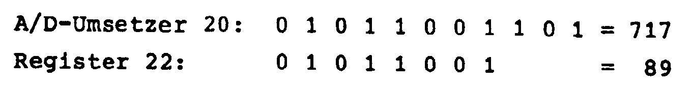
Der nicht berücksichtigte Divisionsrest ergibt sich aus den Binärziffern an den drei den niedrigsten Stellenwerten
zugeordneten Ausgängen des Analog-Digital-Umsetzers 20, die nicht mit dem Register 22 verbunden
sind.The remainder of the division not taken into account results from the binary digits at the three lowest values
assigned outputs of the analog-to-
Im Register 22 kann also der gesamte Wertebereich der analogen Eingangsgröße E nur durch 28 = 256
digitale Werte wiedergegeben werden, die jeweils einem Quantisierungswert mit der begrenzten Auflösung von
8 Bit entsprechen, und der jeweils im Register 22 stehende digitale Zahlenwert entspricht einem dieser 256
Quantisierungswerte unter Vernachlässigung des Quantisierungsrestes.In
Die Ausgänge des Registers 22 sind mit den Modulationssignaleingängen eines digitalen Pulsdauermodulators
24 verbunden, der die gleiche Auflösung von 8 Bit wie das Register 22 hat. Der Pulsdauermodulator
24 entspricht dem Pulsdauermodulator 10 von Fig. 1 und gibt am Ausgang eine pulsdauermodulierte Impulsfolge
I1 ab, deren Impulsperiode durch ein von einem Taktgenerator 26 geliefertes Taktsignal bestimmt ist und
deren Impulse eine Dauer haben, die dem im Register 22 stehenden digitalen Zahlenwert proportional ist. Der
Ausgang des Pulsdauermodulators 24 ist mit dem Signaleingang einer Torschaltung 28 verbunden, deren Steuereingang
mit dem Ausgang einer durch den Taktgenerator 26 synchronisierten Steuerschaltung 30 verbunden
ist, so daß die Torschaltung 28 durch ein von der Steuerschaltung 30 geliefertes Steuersignal S geöffnet oder
geschlossen wird. Der Ausgang derTorschaltung 28 ist über eine Oder-Schaltung 32 mit einer Mittelungsschaltung
34 verbunden, die der Mittelungsschaltung 14 von Fig. 1 entspricht und beispielsweise durch ein Tiefpaßfilter
gebildet sein kann. Wenn die Torschaltung 28 von der Steuerschaltung 30 geöffnet ist, wird somit
die pulsdauermodulierte Impulsfolge I1 zu der Mittelungsschaltung 34 übertragen. Die bisher beschriebenen
Bestandteile der Schaltung von Fig. 2 arbeiten dann in der gleichen Weise wie die zuvor beschriebene Schaltung
von Fig. 1.The outputs of the
Die übrigen Bestandteile der Schaltung von Fig. 2 dienen der Erhöhung der Genauigkeit, mit der die analoge
Eingangsgröße E in das am Ausgang abgegebene Gleichsignal A umgewandelt wird. Zu diesem Zweck
ist ein zweites achtstufiges Register 36 vorgesehen, dessen drei dem niedrigsten Stellenwert zugeordnete Eingänge
mit den drei dem niedrigsten Stellenwert zugeordneten Ausgängen des Analog-Digital-Umsetzers 20
verbunden sind, während die übrigen Eingänge des Registers 36 nicht beschaltet sind. Im Register 36 steht
daher eine achtstellige Dualzahl, deren fünf erste Stellen den Wert "0" haben und in deren drei letzten Stellen
die Binärziffern der drei letzten Stellen der elfstelligen Dualzahl stehen, die vom Analog-Digital-Umsetzer 20
ausgegeben wird.The remaining components of the circuit of Fig. 2 serve to increase the accuracy with which the analog
Input variable E is converted into the direct signal A output at the output. To this end
a second eight-
Die Ausgänge des Registers 36 sind mit einer zugeordneten Gruppe von Eingängen eines Addierers 38
verbunden, dessen zweite Eingangsgruppe mit den Ausgängen des Registers 22 verbunden ist. Der Addierer
38 bildet die Summe der beiden achtstelligen Dualzahlen, die in den Registern 22 und 36 stehen, und gibt eine
dieser Summe entsprechende achtstellige Dualzahl an seinen Ausgängen ab.The outputs of the
Die Ausgänge des Addierers 38 sind mit den Modulationssignaleingängen eines digitalen Pulsdauermodulators
40 verbunden, der von gleicher Art wie der Pulsdauermodulator 24 ist, also die gleiche begrenzte Auflösung
von 8 Bit hat. Der Pulsdauermodulator 40 empfängt ebenfalls das vom Taktgenerator 26 gelieferte Taktsignal
und gibt am Ausgang eine pulsdauermodulierte Impulsfolge I2 ab, deren Impulse die gleiche, durch den
Taktgenerator 26 bestimmte konstante Periode wie die Impulse der Impulsfolge I1 haben und deren Dauer dem
Zahlenwert der vom Addierer 38 abgegebenen Dualzahl proportional ist. Der Ausgang des Pulsdauermodulators
40 ist mit dem Signaleingang einer Torschaltung 42 verbunden, die an ihrem Steuereingang das von der
Steuerschaltung 30 gelieferte Steuersignal S über einen Invertierer 44 empfängt so daß die Torschaltung 42
gegensinnig zu der Torschaltung 28 geöffnet und geschlossen wird. Der Ausgang der Torschaltung 42 ist über
die Oder-Schaltung 32 mit der Mittelungsschaltung 34 verbunden.The outputs of the
Bei der Addition im Addierer 38 werden die Binärziffern der drei letzten Stellen der im Register 36 stehenden
Dualzahl stellengleich zu den Binärziffern der drei letzten Stellen der im Register 22 stehenden Dualzahl
addiert. Bei dem zuvor angegebenen Zahlenbeispiel erfolgt also die Addition nach dem folgenden Schema:

Die drei letzten Stellen der im Register 36 stehenden Dualzahl sind also für die Addition um drei Stellen
in Richtung höherer Stellenwerte verschoben worden, was einer Multiplikation mit dem Faktor 23 = 8 entspricht.
Diese drei Stellen entsprechen dem Divisionsrest, der bei der Pulsdauermodulation im Pulsdauermodulator
24 nicht berücksichtigt worden ist. Bei dem obigen Zahlenbeispiel hat der Divisionsrest den Dezimalwert 0,625;
er geht nun in die Addition mit dem Dezimalwert 0,625·8 = 5 ein.The last three digits of the dual number in
Bezogen auf den Wert der anlogen Eingangsgröße E entspricht die im Register 22 stehende Dualzahl,
wie zuvor erläutert wurde, einem Quantisierungswert der Eingangsgröße E mit der auf 8 Bit begrenzten Auflösung,
wobei der Quantisierungsrest unberücksichtigt bleibt. Der Quantisierungsrest ist nur dann Null, wenn
der Wert der Eingangsgröße E zufällig genau dem Quantisierungswert entspricht. Wenn der Quantisierungsrest
von Null verschieden ist, ist die Impulsdauer der pulsdauermodulierten Impulsfolge I1 um einen dem Quantisierungsrest
proportionalen Betrag kleiner als die Impulsdauer, die dem genauen Wert der Eingangsgröße
E entsprechen würde.Based on the value of the analog input variable E, the dual number in
Demgegenüber entspricht die vom Addierer 38 abgegebene Dualzahl der Summe aus dem im Pulsdauermodulator
24 berücksichtigten Quantisierungswert und aus dem mit dem Faktor 8 multiplizierten Quantisierungsrest,
wobei auch diese Summe mit einer Auflösung von 8 Bit dargestellt ist. Wenn der Quantisierungsrest
von Null verschieden ist, ist also die Impulsdauer der pulsdauermodulierten Impulsfolge I2 um das 7-fache des
Quantisierungsrestes größer als die Impulsdauer, die dem genauen Wert der Eingangsgröße E entsprechen
würde.In contrast, the dual number output by the
Zum besseren Verständnis der Funktionsweise sind die Impulsfolgen I1 und I2 in den mit den gleichen Bezeichnungen
versehenen Diagrammen von Fig. 3 dargestellt. Weitere Diagramme von Fig. 3 zeigen den zeitlichen
Verlauf des von der Steuerschaltung 30 gelieferten Steuersignals S und die am Ausgang der Oder-Schaltung
32 erhaltene Gesamtimpulsfolge IG.For a better understanding of the mode of operation, the pulse sequences I 1 and I 2 are shown in the diagrams from FIG. 3 provided with the same designations. 3 show the time profile of the control signal S supplied by the
Wenn das Steuersignal S den hohen Signalpegel hat, ist die Torschaltung 28 geöffnet und die Torschaltung
42 geschlossen. Wenn das Steuersignal S den niedrigen Signalpegel hat, ist die Torschaltung 42 geöffnet und
die Torschaltung 28 geschlossen.When the control signal S has the high signal level, the
Die Steuerscbaltung 30 ist so ausgebildet, daß das Steuersignal S jeweils für sieben aufeinanderfolgende
Impulsperioden der Impulsfolgen I1 und I2 den hohen Signalpegel und dann für eine Impulsperiode den niedrigen
Signalpegel hat. Die zur Mittelungsschaltung 34 übertragene Gesamtimpulsfolge IG enthält also in jeweils
acht aufeinanderfolgenden Impulsen sieben Impulse der Impulsfolge I1 und einen Impuls der Impulsfolge I2.The
Da die Impulsdauer D2 der Impulse der Impulsfolge 12 gleich der Summe aus der Impulsdauer D1 der Impulsfolge
I1 und aus der dem 8-fachen Quantisierungsrest entsprechenden Dauer D8R ist:
Dies entspricht einer mittleren Impulsdauer DM:
Der von der Mittelungsschaltung 34 gebildete Gleichsignalmittelwert ist dieser mittleren Impulsdauer DM
proportional.The average signal value formed by the averaging
Der Term D8R/8 entspricht einem dem einfachen Quantisierungsrest proportionalen Anteil der Impulsdauer.
Die mittlere Impulsdauer setzt sich also aus einem dem Quantisierungswert proportionalen Anteil und aus einem
dem Quantisierungsrest proportionalen Anteil zusammen. Sie ist somit dem Wert der Eingangsgröße E
mit einer der Berücksichtigung des Quantisierungsrestes entsprechenden höheren Genauigkeit proportional.
Da bei dem gewählten Beispiel der Quantisierungsrest mit einer Auflösung von 3 Bit berücksichtigt wird, ergibt
sich eine Erhöhung der Genauigkeit um den Faktor 23 = 8. Diese erhöhte Genauigkeit bleibt in dem von der
Mittelungsschaltung 34 gebildeten Gleichsignalmittelwert erhalten.The term D 8R / 8 corresponds to a portion of the pulse duration proportional to the simple quantization residue. The mean pulse duration is therefore composed of a portion proportional to the quantization value and a portion proportional to the quantization residue. It is therefore proportional to the value of the input variable E with a higher accuracy corresponding to the consideration of the quantization residue. Since the quantization residue with a resolution of 3 bits is taken into account in the selected example, the accuracy increases by a factor of 2 3 = 8. This increased accuracy is retained in the mean signal value formed by the averaging
Die zuvor beschriebenen Maßnahmen zur Erhöhung der Genauigkeit bestehen also im allgemeinen Fall darin, daß für die Pulsdauermodulation der zweiten Impulsfolge die Summe aus dem für die Modulation der ersten Impulsfolge verwendeten Quantisierungswert und aus dem mit einem Faktor n multiplizierten Quantisierungsrest verwendet wird und daß die für die Mittelung verwendete Impulsfolge derart aus Impulsen der beiden Impulsfolgen zusammengesetzt ist, daß jeweils n aufeinanderfolgende Impulse einen Impuls der zweiten Impulsfolge und (n-1) Impulse der ersten Impulsfolge enthalten. Dann wird der im Impuls der zweiten Impulsfolge zusätzlich enthaltene n-fache Quantisierungsrest im Mittel auf n Impulsperioden aufgeteilt.The measures described above for increasing the accuracy therefore exist in the general case in that for the pulse duration modulation of the second pulse sequence the sum of that for the modulation of the first pulse sequence used quantization value and from the quantization residue multiplied by a factor n is used and that the pulse sequence used for averaging is made up of pulses of two pulse sequences is composed that n consecutive pulses each a pulse of the second Pulse train and (n-1) pulses of the first pulse train included. Then the pulse in the second pulse train additionally contained n-fold quantization residue on average divided into n pulse periods.
Insgesamt muß in der für die Mittelung verwendeten Gesamtimpulsfolge das Verhältnis der Anzahl der Impulse der zweiten Impulsfolge zur Gesamtzahl der Impulse dem Kehrwert des Faktors entsprechen, mit dem der Quantisierungsrest multipliziert wird.Overall, the ratio of the number of Pulses of the second pulse sequence for the total number of pulses correspond to the reciprocal of the factor with which the quantization residue is multiplied.
Durch die beschriebenen Maßnahmen kann mit geringem zusätzlichen Schaltungsaufwand, der sich auf die Verwendung von 8 Bit-Schaltungen beschränkt, eine beträchtliche Erhöhung der Genauigkeit bei der Umwandlung einer Eingangsgröße in ein dazu proportionales Gleichsignal über die der 8 Bit-Auflösung entsprechende Genauigkeit hinaus erzielt werden. Die beschriebene Lösung erweist sich insbesondere deshalb als vorteilhaft, weil im Handel integrierte Schaltungen erhältlich sind, die zwei 8 Bit-Dauermodulatoren enthalten. Es ist daher möglich, den zweiten vorhandenen Pulsdauermodulator zur Erhöhung der Genauigkeit auszunutzen.The measures described can be carried out with little additional circuitry the use of 8 bit circuits limits a significant increase in the accuracy of the conversion an input variable into a proportional signal proportional to it, which corresponds to the 8 bit resolution Accuracy can be achieved. The solution described proves to be particularly useful advantageous because integrated circuits are commercially available which contain two 8-bit permanent modulators. It is therefore possible to use the second pulse duration modulator to increase the accuracy.
Natürlich ist die Erfindung nicht auf den Fall beschränkt, daß die Eingangsgröße als Analogsignal vorliegt,
wie in der vorstehenden Beschreibung als Beispiel angenommen worden ist. Die Eingangsgröße kann durch
ein beliebiges elektrisches Signal dargestellt sein, beispielsweise durch ein digitales Signal, eine Frequenz
oder dergleichen. Wenn beispielsweise die Eingangsgröße durch eine parallele binäre Codegruppe dargestellt
ist, kann derAnalog-Digital-Umsetzer 20 von Fig. 2 durch ein Register ersetzt werden, in dem die Codegruppe
gespeichert wird, oder die parallelen Übertragungsleitungen, über die die Codegruppe übertragen wird, können
direkt mit den Eingängen der Register 22 und 36 verbunden werden. Die in jedem Fall erforderlichen Abänderungen
der Schaltung sind dem Fachmann geläufig.Of course, the invention is not limited to the case where the input variable is available as an analog signal,
as taken as an example in the above description. The input variable can by
any electrical signal can be represented, for example by a digital signal, a frequency
or similar. If, for example, the input variable is represented by a parallel binary code group
2 can be replaced by a register in which the code group
is stored, or the parallel transmission lines over which the code group is transmitted
can be connected directly to the inputs of
Claims (1)
- An arrangement for the conversion of an electrical input quantity (E) into an electrical DC signal (A) proportional thereto, comprising a first digital pulse duration modulator (24) of limited resolution which supplies a first periodic pulse sequence (I1) which is pulse duration modulated with the quantization value of the input quantity which corresponds to the limited resolution neglecting the quantization remainder, a second pulse duration modulator (40) of limited resolution which supplies a second periodic pulse sequence (I2) which is pulse duration modulated dependent on the quantization remainder, and an averaging circuit (34) for forming a DC signal mean value of the pulse duration modulated pulse sequences, characterized in that the second periodic pulse sequence supplied by the second pulse duration modulator (40) is pulse duration modulated with the sum of the quantization value corresponding to the limited resolution and of the quantization remainder multiplied by a predetermined factor, and in that a switching arrangement (28, 30, 42, 44) is provided which selectively transmits the pulses of the two pulse sequences to the averaging circuit (34) in such a manner that the ratio of the number of transmitted pulses of the second periodic pulse sequence (I2) to the total number of transmitted pulses is equal to the reciprocal of the predetermined factor.
Applications Claiming Priority (2)
| Application Number | Priority Date | Filing Date | Title |
|---|---|---|---|
| DE3933491A DE3933491A1 (en) | 1989-10-06 | 1989-10-06 | ARRANGEMENT FOR CONVERTING AN ELECTRICAL INPUT SIZE INTO A PROPORTIONAL ELECTRICAL SIGNAL |
| DE3933491 | 1989-10-06 |
Publications (4)
| Publication Number | Publication Date |
|---|---|
| EP0421395A2 EP0421395A2 (en) | 1991-04-10 |
| EP0421395A3 EP0421395A3 (en) | 1993-04-21 |
| EP0421395B1 EP0421395B1 (en) | 1995-12-20 |
| EP0421395B2 true EP0421395B2 (en) | 1998-11-11 |
Family
ID=6391003
Family Applications (1)
| Application Number | Title | Priority Date | Filing Date |
|---|---|---|---|
| EP90118995A Expired - Lifetime EP0421395B2 (en) | 1989-10-06 | 1990-10-04 | Arrangement for the conversion of an electrical input value to a direct electrical signal proportional thereto |
Country Status (5)
| Country | Link |
|---|---|
| US (1) | US5103462A (en) |
| EP (1) | EP0421395B2 (en) |
| JP (1) | JPH0783267B2 (en) |
| DE (2) | DE3933491A1 (en) |
| FI (1) | FI99179C (en) |
Families Citing this family (14)
| Publication number | Priority date | Publication date | Assignee | Title |
|---|---|---|---|---|
| JP2777291B2 (en) * | 1991-04-30 | 1998-07-16 | 株式会社東芝 | Analog / digital mixed circuit |
| FR2682768A1 (en) * | 1991-10-21 | 1993-04-23 | Otic Fischer & Porter | METHODS OF CONVERTING IMPEDANCE REPORTS APPLICABLE TO MEASURING DEVICES, IN PARTICULAR TO INDUSTRIAL PRESSURE TRANSMITTERS, AND THEIR IMPLEMENTING DEVICES. |
| US5471505A (en) * | 1993-10-01 | 1995-11-28 | Elsag International N.V. | Method and apparatus for increasing the resolution of a digital to analog converted pulse width modulated signal |
| EP0892500B1 (en) | 1997-07-17 | 2003-02-26 | STMicroelectronics S.r.l. | System for increasing the definition in converting a digital datum in a PWM signal for driving a full-bridge output stage |
| JP3601315B2 (en) * | 1997-11-05 | 2004-12-15 | セイコーエプソン株式会社 | Step motor control device, control method, and timing device |
| US5959501A (en) * | 1998-01-14 | 1999-09-28 | Harris Corporation | Class D amplifier with scaled clock and related methods |
| JP2900153B1 (en) * | 1998-02-10 | 1999-06-02 | セイコーインスツルメンツ株式会社 | Analog electronic clock |
| AT409731B (en) * | 1998-10-16 | 2002-10-25 | Fronius Schweissmasch Prod | CONTROL DEVICE FOR A WELDING MACHINE |
| CN100417020C (en) * | 2000-03-23 | 2008-09-03 | 爱立信股份有限公司 | Method and device for generating pulse width modulation signal and optical attenuator controlled by pulse width modulation signal |
| WO2002035893A1 (en) * | 2000-10-25 | 2002-05-02 | Koninklijke Philips Electronics N.V. | Circuit arrangement |
| US6714770B2 (en) * | 2001-11-16 | 2004-03-30 | Aleksander Maksimov | Method and apparatus for prevention of the concurrence of modes condition during operation of electronic device |
| CN1310427C (en) * | 2004-02-25 | 2007-04-11 | 凌阳科技股份有限公司 | Pulse Width Modulation Circuit and Method |
| US8902089B2 (en) * | 2012-05-02 | 2014-12-02 | Qualcomm Incorporated | Systems and methods for performing digital modulation |
| FR2999836B1 (en) * | 2012-12-18 | 2018-11-09 | Safran Electronics & Defense | DIGITAL DIGITAL CONVERSION METHOD WITH OPTIMIZED IMPLULSION WIDTH MODULATION |
Family Cites Families (15)
| Publication number | Priority date | Publication date | Assignee | Title |
|---|---|---|---|---|
| US4112368A (en) * | 1970-07-13 | 1978-09-05 | Westinghouse Electric Corp. | Constant amplitude carrier communications system |
| JPS5149531B2 (en) * | 1971-11-13 | 1976-12-27 | ||
| US3823396A (en) * | 1972-04-17 | 1974-07-09 | Electronics Processors Inc | Digital to analog converter incorporating multiple time division switching circuits |
| GB1553697A (en) * | 1975-07-17 | 1979-10-03 | Licentia Gmbh | Digital to analogue converter arrangements |
| JPS5228205A (en) * | 1975-08-28 | 1977-03-03 | Sony Corp | Station selector unit |
| DE2721993C3 (en) * | 1977-05-14 | 1980-09-18 | Licentia Patent-Verwaltungs-Gmbh, 6000 Frankfurt | Circuit arrangement for the transmission of digital direct current signals by means of carrier oscillations of a given frequency |
| US4334237A (en) * | 1980-02-07 | 1982-06-08 | Rca Corporation | Adaptive amplitude averaging for weighting quantizing noise |
| JPS57155833A (en) * | 1981-03-23 | 1982-09-27 | Toshiba Corp | Digital-to-analog converting circuit |
| JPS5847325A (en) * | 1981-09-17 | 1983-03-19 | Sanyo Electric Co Ltd | Modulating circuit of pulse width |
| JPS5911026A (en) * | 1982-07-12 | 1984-01-20 | Yokogawa Hokushin Electric Corp | Digital-analog converter |
| DE3306334A1 (en) * | 1983-02-23 | 1984-08-23 | Siemens AG, 1000 Berlin und 8000 München | QUANTIZER FOR DPCM CODER |
| GB2144005B (en) * | 1983-07-28 | 1986-10-22 | Rca Corp | Digital-to-analog converter useful in a television receiver |
| JPS6235709A (en) * | 1985-08-09 | 1987-02-16 | Hitachi Ltd | digital circuit |
| US4685114A (en) * | 1986-02-27 | 1987-08-04 | The Charles Stark Draper Laboratory, Inc. | Waveform modulation system |
| JPS62231569A (en) * | 1986-03-31 | 1987-10-12 | Fuji Photo Film Co Ltd | Quantizing method for estimated error |
-
1989
- 1989-10-06 DE DE3933491A patent/DE3933491A1/en active Granted
-
1990
- 1990-09-26 FI FI904733A patent/FI99179C/en not_active IP Right Cessation
- 1990-10-02 US US07/591,696 patent/US5103462A/en not_active Expired - Fee Related
- 1990-10-04 EP EP90118995A patent/EP0421395B2/en not_active Expired - Lifetime
- 1990-10-04 DE DE59009979T patent/DE59009979D1/en not_active Expired - Fee Related
- 1990-10-05 JP JP2266592A patent/JPH0783267B2/en not_active Expired - Lifetime
Also Published As
| Publication number | Publication date |
|---|---|
| FI99179C (en) | 1997-10-10 |
| DE3933491A1 (en) | 1991-04-18 |
| FI904733A0 (en) | 1990-09-26 |
| JPH0783267B2 (en) | 1995-09-06 |
| DE59009979D1 (en) | 1996-02-01 |
| DE3933491C2 (en) | 1991-10-17 |
| EP0421395A3 (en) | 1993-04-21 |
| US5103462A (en) | 1992-04-07 |
| EP0421395B1 (en) | 1995-12-20 |
| JPH03207124A (en) | 1991-09-10 |
| EP0421395A2 (en) | 1991-04-10 |
| FI99179B (en) | 1997-06-30 |
Similar Documents
| Publication | Publication Date | Title |
|---|---|---|
| EP0421395B2 (en) | Arrangement for the conversion of an electrical input value to a direct electrical signal proportional thereto | |
| DE3003099C2 (en) | Digital-to-analog converter with compensation circuit | |
| DE3902313C2 (en) | Analog / digital converter | |
| DE3643161C2 (en) | Method and device for offset voltage correction in an analog / digital converter | |
| DE3587950T2 (en) | Parallel algorithmic digital / analog converter. | |
| DE3129338A1 (en) | SIGNAL CONVERTER | |
| DE3202789A1 (en) | Digital/analog converter circuit | |
| DE2451983C2 (en) | Digital-to-analog converter | |
| DE2836079A1 (en) | DIGITAL-ANALOG CONVERTER | |
| DE2801272C2 (en) | Circuit arrangement for carrying out a weight factor-dependent charge distribution and transfer | |
| DE3237283A1 (en) | ANALOG / DIGITAL CONVERTER | |
| DE3147578C2 (en) | ||
| DE2724347C2 (en) | Delta modulator with a quantizing comparator | |
| DE3685836T2 (en) | INTERPOLATIVE DA CONVERTER. | |
| DE69924013T2 (en) | CAPACITIVE PARALLEL ANALOG DIGITAL TRANSFORMER | |
| DE69409547T2 (en) | DIGITAL-ANALOG CONVERTER WITH LOW RESOLUTION AND HIGH LINEARITY WITHOUT TRIM | |
| DE2900383C2 (en) | Interpolative PCM decoder | |
| DE69521452T2 (en) | Circuit for digital / analog conversion and the circuit using A / D converter | |
| DE2804915C2 (en) | ||
| DE2229398A1 (en) | Differential pulse code modulation system with periodic change in the modulator step | |
| DE3046772C2 (en) | Clock generator | |
| DE2439712C2 (en) | PCM encoder | |
| EP0265637B1 (en) | Pulse shaper | |
| DE69414538T2 (en) | Digital / analog converter circuit | |
| DE3124194A1 (en) | "FREQUENCY DETECTION" |
Legal Events
| Date | Code | Title | Description |
|---|---|---|---|
| PUAI | Public reference made under article 153(3) epc to a published international application that has entered the european phase |
Free format text: ORIGINAL CODE: 0009012 |
|
| AK | Designated contracting states |
Kind code of ref document: A2 Designated state(s): CH DE FR GB IT LI |
|
| PUAL | Search report despatched |
Free format text: ORIGINAL CODE: 0009013 |
|
| AK | Designated contracting states |
Kind code of ref document: A3 Designated state(s): CH DE FR GB IT LI |
|
| 17P | Request for examination filed |
Effective date: 19930625 |
|
| 17Q | First examination report despatched |
Effective date: 19950531 |
|
| GRAA | (expected) grant |
Free format text: ORIGINAL CODE: 0009210 |
|
| ITF | It: translation for a ep patent filed | ||
| AK | Designated contracting states |
Kind code of ref document: B1 Designated state(s): CH DE FR GB IT LI |
|
| REF | Corresponds to: |
Ref document number: 59009979 Country of ref document: DE Date of ref document: 19960201 |
|
| REG | Reference to a national code |
Ref country code: CH Ref legal event code: NV Representative=s name: DIPL.-ING. VOLKER MORSTADT |
|
| ET | Fr: translation filed | ||
| GBT | Gb: translation of ep patent filed (gb section 77(6)(a)/1977) |
Effective date: 19960327 |
|
| PLBQ | Unpublished change to opponent data |
Free format text: ORIGINAL CODE: EPIDOS OPPO |
|
| PLBI | Opposition filed |
Free format text: ORIGINAL CODE: 0009260 |
|
| PLBF | Reply of patent proprietor to notice(s) of opposition |
Free format text: ORIGINAL CODE: EPIDOS OBSO |
|
| 26 | Opposition filed |
Opponent name: KROHNE MESSTECHNIK GMBH & CO. KG Effective date: 19960920 |
|
| PLBF | Reply of patent proprietor to notice(s) of opposition |
Free format text: ORIGINAL CODE: EPIDOS OBSO |
|
| PLBF | Reply of patent proprietor to notice(s) of opposition |
Free format text: ORIGINAL CODE: EPIDOS OBSO |
|
| PLAW | Interlocutory decision in opposition |
Free format text: ORIGINAL CODE: EPIDOS IDOP |
|
| PLAW | Interlocutory decision in opposition |
Free format text: ORIGINAL CODE: EPIDOS IDOP |
|
| PUAH | Patent maintained in amended form |
Free format text: ORIGINAL CODE: 0009272 |
|
| STAA | Information on the status of an ep patent application or granted ep patent |
Free format text: STATUS: PATENT MAINTAINED AS AMENDED |
|
| 27A | Patent maintained in amended form |
Effective date: 19981111 |
|
| AK | Designated contracting states |
Kind code of ref document: B2 Designated state(s): CH DE FR GB IT LI |
|
| REG | Reference to a national code |
Ref country code: CH Ref legal event code: AEN Free format text: AUFRECHTERHALTUNG DES PATENTES IN GEAENDERTER FORM |
|
| GBTA | Gb: translation of amended ep patent filed (gb section 77(6)(b)/1977) | ||
| ET3 | Fr: translation filed ** decision concerning opposition | ||
| PGFP | Annual fee paid to national office [announced via postgrant information from national office to epo] |
Ref country code: CH Payment date: 19990915 Year of fee payment: 10 |
|
| PGFP | Annual fee paid to national office [announced via postgrant information from national office to epo] |
Ref country code: DE Payment date: 20001005 Year of fee payment: 11 |
|
| PGFP | Annual fee paid to national office [announced via postgrant information from national office to epo] |
Ref country code: FR Payment date: 20001012 Year of fee payment: 11 |
|
| PG25 | Lapsed in a contracting state [announced via postgrant information from national office to epo] |
Ref country code: LI Free format text: LAPSE BECAUSE OF NON-PAYMENT OF DUE FEES Effective date: 20001031 Ref country code: CH Free format text: LAPSE BECAUSE OF NON-PAYMENT OF DUE FEES Effective date: 20001031 |
|
| REG | Reference to a national code |
Ref country code: CH Ref legal event code: PL |
|
| PGFP | Annual fee paid to national office [announced via postgrant information from national office to epo] |
Ref country code: GB Payment date: 20010914 Year of fee payment: 12 |
|
| REG | Reference to a national code |
Ref country code: GB Ref legal event code: IF02 |
|
| PG25 | Lapsed in a contracting state [announced via postgrant information from national office to epo] |
Ref country code: FR Free format text: LAPSE BECAUSE OF NON-PAYMENT OF DUE FEES Effective date: 20020628 |
|
| PG25 | Lapsed in a contracting state [announced via postgrant information from national office to epo] |
Ref country code: DE Free format text: LAPSE BECAUSE OF NON-PAYMENT OF DUE FEES Effective date: 20020702 |
|
| REG | Reference to a national code |
Ref country code: FR Ref legal event code: ST |
|
| PG25 | Lapsed in a contracting state [announced via postgrant information from national office to epo] |
Ref country code: GB Free format text: LAPSE BECAUSE OF NON-PAYMENT OF DUE FEES Effective date: 20021004 |
|
| GBPC | Gb: european patent ceased through non-payment of renewal fee |
Effective date: 20021004 |
|
| PG25 | Lapsed in a contracting state [announced via postgrant information from national office to epo] |
Ref country code: IT Free format text: LAPSE BECAUSE OF NON-PAYMENT OF DUE FEES;WARNING: LAPSES OF ITALIAN PATENTS WITH EFFECTIVE DATE BEFORE 2007 MAY HAVE OCCURRED AT ANY TIME BEFORE 2007. THE CORRECT EFFECTIVE DATE MAY BE DIFFERENT FROM THE ONE RECORDED. Effective date: 20051004 |
|
| PLAB | Opposition data, opponent's data or that of the opponent's representative modified |
Free format text: ORIGINAL CODE: 0009299OPPO |