EP0416805B1 - Transistor comportant un limiteur de tension - Google Patents
Transistor comportant un limiteur de tension Download PDFInfo
- Publication number
- EP0416805B1 EP0416805B1 EP90309443A EP90309443A EP0416805B1 EP 0416805 B1 EP0416805 B1 EP 0416805B1 EP 90309443 A EP90309443 A EP 90309443A EP 90309443 A EP90309443 A EP 90309443A EP 0416805 B1 EP0416805 B1 EP 0416805B1
- Authority
- EP
- European Patent Office
- Prior art keywords
- region
- transistor
- cell
- annular
- type
- Prior art date
- Legal status (The legal status is an assumption and is not a legal conclusion. Google has not performed a legal analysis and makes no representation as to the accuracy of the status listed.)
- Expired - Lifetime
Links
- 230000015556 catabolic process Effects 0.000 claims description 37
- 239000004065 semiconductor Substances 0.000 claims description 25
- 229910021420 polycrystalline silicon Inorganic materials 0.000 claims description 22
- 238000000034 method Methods 0.000 claims description 9
- 238000004519 manufacturing process Methods 0.000 claims description 8
- 230000005669 field effect Effects 0.000 claims description 5
- 210000000746 body region Anatomy 0.000 description 20
- 239000000758 substrate Substances 0.000 description 20
- VYPSYNLAJGMNEJ-UHFFFAOYSA-N Silicium dioxide Chemical compound O=[Si]=O VYPSYNLAJGMNEJ-UHFFFAOYSA-N 0.000 description 16
- 229920005591 polysilicon Polymers 0.000 description 16
- 238000009792 diffusion process Methods 0.000 description 11
- 235000012239 silicon dioxide Nutrition 0.000 description 8
- 239000000377 silicon dioxide Substances 0.000 description 8
- 239000007943 implant Substances 0.000 description 5
- 150000002500 ions Chemical class 0.000 description 5
- 230000008901 benefit Effects 0.000 description 4
- ZOXJGFHDIHLPTG-UHFFFAOYSA-N Boron Chemical compound [B] ZOXJGFHDIHLPTG-UHFFFAOYSA-N 0.000 description 3
- OAICVXFJPJFONN-UHFFFAOYSA-N Phosphorus Chemical compound [P] OAICVXFJPJFONN-UHFFFAOYSA-N 0.000 description 3
- XUIMIQQOPSSXEZ-UHFFFAOYSA-N Silicon Chemical compound [Si] XUIMIQQOPSSXEZ-UHFFFAOYSA-N 0.000 description 3
- 229910052785 arsenic Inorganic materials 0.000 description 3
- RQNWIZPPADIBDY-UHFFFAOYSA-N arsenic atom Chemical compound [As] RQNWIZPPADIBDY-UHFFFAOYSA-N 0.000 description 3
- 229910052796 boron Inorganic materials 0.000 description 3
- 239000004020 conductor Substances 0.000 description 3
- 230000000694 effects Effects 0.000 description 3
- 230000005684 electric field Effects 0.000 description 3
- 238000005468 ion implantation Methods 0.000 description 3
- 229910052698 phosphorus Inorganic materials 0.000 description 3
- 239000011574 phosphorus Substances 0.000 description 3
- 229910052710 silicon Inorganic materials 0.000 description 3
- 239000010703 silicon Substances 0.000 description 3
- 229910052782 aluminium Inorganic materials 0.000 description 2
- XAGFODPZIPBFFR-UHFFFAOYSA-N aluminium Chemical compound [Al] XAGFODPZIPBFFR-UHFFFAOYSA-N 0.000 description 2
- 239000013078 crystal Substances 0.000 description 2
- 238000010438 heat treatment Methods 0.000 description 2
- 238000002347 injection Methods 0.000 description 2
- 239000007924 injection Substances 0.000 description 2
- 239000000463 material Substances 0.000 description 2
- 229910044991 metal oxide Inorganic materials 0.000 description 2
- 150000004706 metal oxides Chemical class 0.000 description 2
- 238000002161 passivation Methods 0.000 description 2
- 229920002120 photoresistant polymer Polymers 0.000 description 2
- 229910052582 BN Inorganic materials 0.000 description 1
- PZNSFCLAULLKQX-UHFFFAOYSA-N Boron nitride Chemical compound N#B PZNSFCLAULLKQX-UHFFFAOYSA-N 0.000 description 1
- 229910052581 Si3N4 Inorganic materials 0.000 description 1
- 230000015572 biosynthetic process Effects 0.000 description 1
- 239000005380 borophosphosilicate glass Substances 0.000 description 1
- 238000005229 chemical vapour deposition Methods 0.000 description 1
- 230000001066 destructive effect Effects 0.000 description 1
- 239000002019 doping agent Substances 0.000 description 1
- 238000005516 engineering process Methods 0.000 description 1
- 238000002513 implantation Methods 0.000 description 1
- 239000012535 impurity Substances 0.000 description 1
- 230000000873 masking effect Effects 0.000 description 1
- 238000001465 metallisation Methods 0.000 description 1
- 238000000059 patterning Methods 0.000 description 1
- 239000005360 phosphosilicate glass Substances 0.000 description 1
- 230000003252 repetitive effect Effects 0.000 description 1
- HQVNEWCFYHHQES-UHFFFAOYSA-N silicon nitride Chemical compound N12[Si]34N5[Si]62N3[Si]51N64 HQVNEWCFYHHQES-UHFFFAOYSA-N 0.000 description 1
- 239000000344 soap Substances 0.000 description 1
Images


Classifications
-
- H—ELECTRICITY
- H01—ELECTRIC ELEMENTS
- H01L—SEMICONDUCTOR DEVICES NOT COVERED BY CLASS H10
- H01L29/00—Semiconductor devices adapted for rectifying, amplifying, oscillating or switching, or capacitors or resistors with at least one potential-jump barrier or surface barrier, e.g. PN junction depletion layer or carrier concentration layer; Details of semiconductor bodies or of electrodes thereof ; Multistep manufacturing processes therefor
- H01L29/66—Types of semiconductor device ; Multistep manufacturing processes therefor
- H01L29/66007—Multistep manufacturing processes
- H01L29/66075—Multistep manufacturing processes of devices having semiconductor bodies comprising group 14 or group 13/15 materials
- H01L29/66227—Multistep manufacturing processes of devices having semiconductor bodies comprising group 14 or group 13/15 materials the devices being controllable only by the electric current supplied or the electric potential applied, to an electrode which does not carry the current to be rectified, amplified or switched, e.g. three-terminal devices
- H01L29/66409—Unipolar field-effect transistors
- H01L29/66477—Unipolar field-effect transistors with an insulated gate, i.e. MISFET
- H01L29/66674—DMOS transistors, i.e. MISFETs with a channel accommodating body or base region adjoining a drain drift region
- H01L29/66712—Vertical DMOS transistors, i.e. VDMOS transistors
-
- H—ELECTRICITY
- H01—ELECTRIC ELEMENTS
- H01L—SEMICONDUCTOR DEVICES NOT COVERED BY CLASS H10
- H01L29/00—Semiconductor devices adapted for rectifying, amplifying, oscillating or switching, or capacitors or resistors with at least one potential-jump barrier or surface barrier, e.g. PN junction depletion layer or carrier concentration layer; Details of semiconductor bodies or of electrodes thereof ; Multistep manufacturing processes therefor
- H01L29/02—Semiconductor bodies ; Multistep manufacturing processes therefor
- H01L29/06—Semiconductor bodies ; Multistep manufacturing processes therefor characterised by their shape; characterised by the shapes, relative sizes, or dispositions of the semiconductor regions ; characterised by the concentration or distribution of impurities within semiconductor regions
- H01L29/0603—Semiconductor bodies ; Multistep manufacturing processes therefor characterised by their shape; characterised by the shapes, relative sizes, or dispositions of the semiconductor regions ; characterised by the concentration or distribution of impurities within semiconductor regions characterised by particular constructional design considerations, e.g. for preventing surface leakage, for controlling electric field concentration or for internal isolations regions
- H01L29/0607—Semiconductor bodies ; Multistep manufacturing processes therefor characterised by their shape; characterised by the shapes, relative sizes, or dispositions of the semiconductor regions ; characterised by the concentration or distribution of impurities within semiconductor regions characterised by particular constructional design considerations, e.g. for preventing surface leakage, for controlling electric field concentration or for internal isolations regions for preventing surface leakage or controlling electric field concentration
- H01L29/0611—Semiconductor bodies ; Multistep manufacturing processes therefor characterised by their shape; characterised by the shapes, relative sizes, or dispositions of the semiconductor regions ; characterised by the concentration or distribution of impurities within semiconductor regions characterised by particular constructional design considerations, e.g. for preventing surface leakage, for controlling electric field concentration or for internal isolations regions for preventing surface leakage or controlling electric field concentration for increasing or controlling the breakdown voltage of reverse biased devices
- H01L29/0615—Semiconductor bodies ; Multistep manufacturing processes therefor characterised by their shape; characterised by the shapes, relative sizes, or dispositions of the semiconductor regions ; characterised by the concentration or distribution of impurities within semiconductor regions characterised by particular constructional design considerations, e.g. for preventing surface leakage, for controlling electric field concentration or for internal isolations regions for preventing surface leakage or controlling electric field concentration for increasing or controlling the breakdown voltage of reverse biased devices by the doping profile or the shape or the arrangement of the PN junction, or with supplementary regions, e.g. junction termination extension [JTE]
- H01L29/0626—Semiconductor bodies ; Multistep manufacturing processes therefor characterised by their shape; characterised by the shapes, relative sizes, or dispositions of the semiconductor regions ; characterised by the concentration or distribution of impurities within semiconductor regions characterised by particular constructional design considerations, e.g. for preventing surface leakage, for controlling electric field concentration or for internal isolations regions for preventing surface leakage or controlling electric field concentration for increasing or controlling the breakdown voltage of reverse biased devices by the doping profile or the shape or the arrangement of the PN junction, or with supplementary regions, e.g. junction termination extension [JTE] with a localised breakdown region, e.g. built-in avalanching region
-
- H—ELECTRICITY
- H01—ELECTRIC ELEMENTS
- H01L—SEMICONDUCTOR DEVICES NOT COVERED BY CLASS H10
- H01L29/00—Semiconductor devices adapted for rectifying, amplifying, oscillating or switching, or capacitors or resistors with at least one potential-jump barrier or surface barrier, e.g. PN junction depletion layer or carrier concentration layer; Details of semiconductor bodies or of electrodes thereof ; Multistep manufacturing processes therefor
- H01L29/02—Semiconductor bodies ; Multistep manufacturing processes therefor
- H01L29/06—Semiconductor bodies ; Multistep manufacturing processes therefor characterised by their shape; characterised by the shapes, relative sizes, or dispositions of the semiconductor regions ; characterised by the concentration or distribution of impurities within semiconductor regions
- H01L29/0684—Semiconductor bodies ; Multistep manufacturing processes therefor characterised by their shape; characterised by the shapes, relative sizes, or dispositions of the semiconductor regions ; characterised by the concentration or distribution of impurities within semiconductor regions characterised by the shape, relative sizes or dispositions of the semiconductor regions or junctions between the regions
- H01L29/0688—Semiconductor bodies ; Multistep manufacturing processes therefor characterised by their shape; characterised by the shapes, relative sizes, or dispositions of the semiconductor regions ; characterised by the concentration or distribution of impurities within semiconductor regions characterised by the shape, relative sizes or dispositions of the semiconductor regions or junctions between the regions characterised by the particular shape of a junction between semiconductor regions
-
- H—ELECTRICITY
- H01—ELECTRIC ELEMENTS
- H01L—SEMICONDUCTOR DEVICES NOT COVERED BY CLASS H10
- H01L29/00—Semiconductor devices adapted for rectifying, amplifying, oscillating or switching, or capacitors or resistors with at least one potential-jump barrier or surface barrier, e.g. PN junction depletion layer or carrier concentration layer; Details of semiconductor bodies or of electrodes thereof ; Multistep manufacturing processes therefor
- H01L29/02—Semiconductor bodies ; Multistep manufacturing processes therefor
- H01L29/06—Semiconductor bodies ; Multistep manufacturing processes therefor characterised by their shape; characterised by the shapes, relative sizes, or dispositions of the semiconductor regions ; characterised by the concentration or distribution of impurities within semiconductor regions
- H01L29/0684—Semiconductor bodies ; Multistep manufacturing processes therefor characterised by their shape; characterised by the shapes, relative sizes, or dispositions of the semiconductor regions ; characterised by the concentration or distribution of impurities within semiconductor regions characterised by the shape, relative sizes or dispositions of the semiconductor regions or junctions between the regions
- H01L29/0692—Surface layout
- H01L29/0696—Surface layout of cellular field-effect devices, e.g. multicellular DMOS transistors or IGBTs
-
- H—ELECTRICITY
- H01—ELECTRIC ELEMENTS
- H01L—SEMICONDUCTOR DEVICES NOT COVERED BY CLASS H10
- H01L29/00—Semiconductor devices adapted for rectifying, amplifying, oscillating or switching, or capacitors or resistors with at least one potential-jump barrier or surface barrier, e.g. PN junction depletion layer or carrier concentration layer; Details of semiconductor bodies or of electrodes thereof ; Multistep manufacturing processes therefor
- H01L29/02—Semiconductor bodies ; Multistep manufacturing processes therefor
- H01L29/06—Semiconductor bodies ; Multistep manufacturing processes therefor characterised by their shape; characterised by the shapes, relative sizes, or dispositions of the semiconductor regions ; characterised by the concentration or distribution of impurities within semiconductor regions
- H01L29/10—Semiconductor bodies ; Multistep manufacturing processes therefor characterised by their shape; characterised by the shapes, relative sizes, or dispositions of the semiconductor regions ; characterised by the concentration or distribution of impurities within semiconductor regions with semiconductor regions connected to an electrode not carrying current to be rectified, amplified or switched and such electrode being part of a semiconductor device which comprises three or more electrodes
- H01L29/1095—Body region, i.e. base region, of DMOS transistors or IGBTs
-
- H—ELECTRICITY
- H01—ELECTRIC ELEMENTS
- H01L—SEMICONDUCTOR DEVICES NOT COVERED BY CLASS H10
- H01L29/00—Semiconductor devices adapted for rectifying, amplifying, oscillating or switching, or capacitors or resistors with at least one potential-jump barrier or surface barrier, e.g. PN junction depletion layer or carrier concentration layer; Details of semiconductor bodies or of electrodes thereof ; Multistep manufacturing processes therefor
- H01L29/40—Electrodes ; Multistep manufacturing processes therefor
- H01L29/41—Electrodes ; Multistep manufacturing processes therefor characterised by their shape, relative sizes or dispositions
- H01L29/423—Electrodes ; Multistep manufacturing processes therefor characterised by their shape, relative sizes or dispositions not carrying the current to be rectified, amplified or switched
- H01L29/42312—Gate electrodes for field effect devices
- H01L29/42316—Gate electrodes for field effect devices for field-effect transistors
- H01L29/4232—Gate electrodes for field effect devices for field-effect transistors with insulated gate
- H01L29/42372—Gate electrodes for field effect devices for field-effect transistors with insulated gate characterised by the conducting layer, e.g. the length, the sectional shape or the lay-out
- H01L29/4238—Gate electrodes for field effect devices for field-effect transistors with insulated gate characterised by the conducting layer, e.g. the length, the sectional shape or the lay-out characterised by the surface lay-out
-
- H—ELECTRICITY
- H01—ELECTRIC ELEMENTS
- H01L—SEMICONDUCTOR DEVICES NOT COVERED BY CLASS H10
- H01L29/00—Semiconductor devices adapted for rectifying, amplifying, oscillating or switching, or capacitors or resistors with at least one potential-jump barrier or surface barrier, e.g. PN junction depletion layer or carrier concentration layer; Details of semiconductor bodies or of electrodes thereof ; Multistep manufacturing processes therefor
- H01L29/66—Types of semiconductor device ; Multistep manufacturing processes therefor
- H01L29/66007—Multistep manufacturing processes
- H01L29/66075—Multistep manufacturing processes of devices having semiconductor bodies comprising group 14 or group 13/15 materials
- H01L29/66227—Multistep manufacturing processes of devices having semiconductor bodies comprising group 14 or group 13/15 materials the devices being controllable only by the electric current supplied or the electric potential applied, to an electrode which does not carry the current to be rectified, amplified or switched, e.g. three-terminal devices
- H01L29/66234—Bipolar junction transistors [BJT]
- H01L29/66325—Bipolar junction transistors [BJT] controlled by field-effect, e.g. insulated gate bipolar transistors [IGBT]
- H01L29/66333—Vertical insulated gate bipolar transistors
-
- H—ELECTRICITY
- H01—ELECTRIC ELEMENTS
- H01L—SEMICONDUCTOR DEVICES NOT COVERED BY CLASS H10
- H01L29/00—Semiconductor devices adapted for rectifying, amplifying, oscillating or switching, or capacitors or resistors with at least one potential-jump barrier or surface barrier, e.g. PN junction depletion layer or carrier concentration layer; Details of semiconductor bodies or of electrodes thereof ; Multistep manufacturing processes therefor
- H01L29/66—Types of semiconductor device ; Multistep manufacturing processes therefor
- H01L29/68—Types of semiconductor device ; Multistep manufacturing processes therefor controllable by only the electric current supplied, or only the electric potential applied, to an electrode which does not carry the current to be rectified, amplified or switched
- H01L29/70—Bipolar devices
- H01L29/72—Transistor-type devices, i.e. able to continuously respond to applied control signals
- H01L29/739—Transistor-type devices, i.e. able to continuously respond to applied control signals controlled by field-effect, e.g. bipolar static induction transistors [BSIT]
- H01L29/7393—Insulated gate bipolar mode transistors, i.e. IGBT; IGT; COMFET
- H01L29/7395—Vertical transistors, e.g. vertical IGBT
-
- H—ELECTRICITY
- H01—ELECTRIC ELEMENTS
- H01L—SEMICONDUCTOR DEVICES NOT COVERED BY CLASS H10
- H01L29/00—Semiconductor devices adapted for rectifying, amplifying, oscillating or switching, or capacitors or resistors with at least one potential-jump barrier or surface barrier, e.g. PN junction depletion layer or carrier concentration layer; Details of semiconductor bodies or of electrodes thereof ; Multistep manufacturing processes therefor
- H01L29/66—Types of semiconductor device ; Multistep manufacturing processes therefor
- H01L29/68—Types of semiconductor device ; Multistep manufacturing processes therefor controllable by only the electric current supplied, or only the electric potential applied, to an electrode which does not carry the current to be rectified, amplified or switched
- H01L29/70—Bipolar devices
- H01L29/74—Thyristor-type devices, e.g. having four-zone regenerative action
- H01L29/744—Gate-turn-off devices
- H01L29/745—Gate-turn-off devices with turn-off by field effect
- H01L29/7455—Gate-turn-off devices with turn-off by field effect produced by an insulated gate structure
-
- H—ELECTRICITY
- H01—ELECTRIC ELEMENTS
- H01L—SEMICONDUCTOR DEVICES NOT COVERED BY CLASS H10
- H01L29/00—Semiconductor devices adapted for rectifying, amplifying, oscillating or switching, or capacitors or resistors with at least one potential-jump barrier or surface barrier, e.g. PN junction depletion layer or carrier concentration layer; Details of semiconductor bodies or of electrodes thereof ; Multistep manufacturing processes therefor
- H01L29/66—Types of semiconductor device ; Multistep manufacturing processes therefor
- H01L29/68—Types of semiconductor device ; Multistep manufacturing processes therefor controllable by only the electric current supplied, or only the electric potential applied, to an electrode which does not carry the current to be rectified, amplified or switched
- H01L29/76—Unipolar devices, e.g. field effect transistors
- H01L29/772—Field effect transistors
- H01L29/78—Field effect transistors with field effect produced by an insulated gate
- H01L29/7801—DMOS transistors, i.e. MISFETs with a channel accommodating body or base region adjoining a drain drift region
- H01L29/7802—Vertical DMOS transistors, i.e. VDMOS transistors
- H01L29/7803—Vertical DMOS transistors, i.e. VDMOS transistors structurally associated with at least one other device
- H01L29/7808—Vertical DMOS transistors, i.e. VDMOS transistors structurally associated with at least one other device the other device being a breakdown diode, e.g. Zener diode
Definitions
- This invention relates to a transistor and method for making a transistor with a voltage clamp.
- the invention can be applied to a power switching transistor, such as a DMOS or insulated gate bipolar transistor.
- a DMOS transistor is disclosed in JP-A-59149058.
- DMOSFET's double diffused metal oxide silicon field effect transistors
- IGBT's insulated gate bipolar transistors
- a typical example of one cell of a DMOSFET transistor is shown in Figure 1A.
- the DMOSFET is a field effect transistor as shown having source regions 10a and 10b formed respectively in body regions 12a, 12b which are in turn formed in an epitaxial layer 14 (i.e., a drain region) grown on a substrate 16.
- a gate 18 is formed over an insulating layer 20 on the principal surface 22 of the epitaxial layer 14.
- a drain contact 24 is attached to the backside of the substrate 16.
- a gate contact 28 and source/body contact 30 are also provided.
- Figure 1A thus shows a conventional power DMOSFET.
- IGBT insulated gate bipolar transistor
- DMOSFET dielectric field effect transistor
- the IGBT in effect is internally a field effect transistor (FET) with its source connected to the collector of a wide base bipolar transistor and its drain connected to the base of the wide base bipolar transistor.
- FET field effect transistor
- the emitter terminal of the wide base transistor then is referred to as the collector terminal of the IGBT; the collector terminal of the wide base transistor is referred to as the IGBT emitter terminal, and the FET gate terminal is the IGBT gate terminal.
- the epitaxial layer 14 is the base region.
- the body regions 12a, 12b are shorted to the IGBT emitter regions 10a, 10b.
- the substrate 16 (which is of P+ type) is the IGBT collector region.
- an insulated gate bipolar transistor and a DMOSFET is in the conductivity type of the substrate.
- the epitaxial region is an open base region, meaning there is no electrical contact of that region to any external structures. This structure is also referred to as a floating base region.
- Prior art power transistors typically include many (e.g., ten thousand) cells of the kind shown in Figure 1A, each cell being identical.
- each cell 34, 36, 38, 40 is a polygon such as a square which includes a central P+ source region 34a, 36a, 38a, 40a formed in and surrounded by an N+ body region 34b, 36b, 38b, 40b.
- Each cell 34, 36, 38, 40 is in turn surrounded by a polycrystalline silicon (i.e., polysilicon) conductive gate region 44 which is the conductive gate region for the entire transistor.
- Each cell typically includes a linear P+ source region formed in between linear N+ body regions. Between adjacent cells a polysilicon gate region is provided.
- a diffused region such as collector region 12a (which is typically delineated by means of a window in a photo-etched oxide mask) is parallel plane in shape, with the exception of part of the region defined by the edge of the window in the oxide.
- the region takes on a cylindrical shape in cross section.
- the space charge lines at the window edge are distorted, resulting in an electric field that is different from the parallel plane electric field structure.
- the peak electric field is higher for the cylindrical junction than for the parallel plane junction.
- the breakdown voltage is lower for the cylindrical junction than for the parallel plane, and so breakdown tends to occur at the cylindrical junction.
- spherical junction is formed at the curved region where two cylindrical junctions meet, such as at the corner of a rectangular shaped diffused region.
- the electrical breakdown of a spherical junction typically occurs at an even lower breakdown voltage than is experienced with a cylindrical junction. This is because extremely small curvature radii are encountered at such sharp corner regions associated with a diffusion area which is masked through a rectangular window.
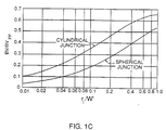
- Figure 1C shows that the breakdown voltage of a spherical junction is lower than the breakdown voltage of a cylindrical junction.
- the breakdown voltage of the spherical junction is typically about 60% of that of a cylindrical junction, where the radius of the junction divided by the thickness of the lightly-doped semiconductor is approximately 0.1.
- r j is the radius of the junction
- W′ is the thickness of the lightly-doped semiconductor.
- BV/BV pp is the breakdown voltage relative to that of a parallel plane.
- the prior art power DMOS and insulated gate bipolar transistor devices typically have spherical or at best cylindrical shaped PN junctions. As indicated above, the spherical junctions typically break down at lower voltage values than do the cylindrical junctions. As also indicated above, a cylindrical junction breaks down at a lower voltage value than does a planar junction.
- Bencuya et al. disclose an improved insulated gate bipolar transistor having a high conductivity collector well surrounding the active portion of the transistor. This collector well prevents undesirable transistor latching. Latching is a phenomenon whereby a semiconductor structure "latches" into a self-perpetuating state of bipolar conduction, which cannot be turned off by removing the voltage bias on the gate to stop FET mode conduction.
- Bencuya et al. do not disclose any method of dealing with the breakdown problem.
- a transistor comprises a plurality of cells wherein each cell comprises a semiconductor body of a first conductivity type, a substantially annular first region of a second conductivity type formed in the semiconductor body, a second region of the first conductivity type formed in the annular region, and a conductive gate region overlying a surface of the semiconductor body and having its extent defined by the interior portion of the second region, characterised by a clamping region of the second conductivity type formed in the interior portion of the first and second regions, the clamping region having a breakdown voltage lower than the breakdown voltage of the other portions of the cell, a cross-sectional shape different from that of the annular first region, and a depth of a doping level the same as that of the annular first region.
- a method of making a cell for a transistor comprising a plurality of cells comprises the steps of forming in a semiconductor body of a first conductivity type a substantially annular first region of a second conductivity type, forming a second region of the first conductivity type in the annular region, and forming a conductive gate region overlying a surface of the semiconductor body and having its extent defined by the interior portion of the second region, characterised by forming a clamping region of the second conductivity type in the interior portion of the first and second regions, the clamping region having a breakdown voltage lower than the breakdown voltage of the other portions of the cell, a cross-sectional shape differing from that of the annular first region, and a depth and a doping level the same as that of the annular first region.
- the clamping region has a voltage breakdown lower than the voltage breakdown of the remainder of the transistor, thus protecting the transistor from destructive voltage breakdown and hence increasing the transistor's safe operating area (SOA).
- the transistor is either an insulated gate bipolar transistor (IGBT) or a double diffused metal oxide semiconductor field effect transistor (DMOSFET).
- IGBT insulated gate bipolar transistor
- DMOSFET double diffused metal oxide semiconductor field effect transistor
- the clamping region has a spherical cross sectional shape so as to achieve a relatively low breakdown voltage.
- the clamping region is formed in the center of a substantially annular (ring-shaped) active region of the transistor cell.
- multiple clamping regions are provided in each cell, with the multiple clamping regions arranged symmetrically.
- the gate region of the cell surrounds the clamping region.
- the active regions of the cell i.e., the source and body for the DMOSFET or emitter and body for the IGBT
- the annular shaped active device cell encloses an island semiconductor region which acts as a voltage clamp. Since the active device cell is annular in shape, it has a higher breakdown voltage than would a cylindrical junction. On the other hand, the clamping region has a spherical cross-sectional shape, so breakdown will always occur around the clamping region junction rather than around the active device region junction.
- the clamping region in the case of the DMOSFET preferably forms a high voltage zener diode.
- discrete zener diodes are conventionally used because they always break down at a particular voltage and can break down repeatedly without being damaged. Therefore, provision of a zener diode in the substrate in accordance with the invention ensures that the breakdown phenomena occurs in the bulk of the epitaxial layer and protects the active device.
- the clamping region preferably forms a portion of a PNP-bipolar junction transistor.
- Both of these embodiments of the invention improve the safe operating area (SOA) of the power transistor, because a zener diode has a superior safe operating area than does a DMOSFET, and similarly a PNP-BJT has a superior safe operating area than does an insulated gate bipolar transistor.
- SOA safe operating area
- a transistor in accordance with the invention can carry a higher current than does a prior art transistor.
- the above described embodiments of the invention also beneficially prevent latching for the same reasons as does the transistor disclosed by Bencuya et al. in U.S. Patent No. 4,779,123 as described above.
- Figure 2 shows a top view of one embodiment of the present invention.
- Figure 2 shows only a small portion of the transistor; it is understood that the pattern shown in Figure 2 is replicated many times for the entire transistor.
- P+ region 40 is the clamping region which is at the center of a preferably substantially radially symmetric i.e., square) active cell 42 of the device.
- the active cell 42 includes the N+ source (for a DMOSFET) or emitter for an IGBT) region 44a, 44b which in this embodiment is square in shape.
- the polysilicon gate region 46 for cell 42 is shown. Shown adjacent to the cell 42 are portions of the adjacent cells 50, 52, 54, 56, 58.
- the polysilicon gate region 46 of cell 42 is connected by polysilicon "bridges" 46a, 46b, 46c (which overlie the body regions 48a, 48b) to respectively the polysilicon gates 52b, 54b, 58b of adjacent cells 52, 54, and 58.
- the polysilicon bridges advantageously eliminate the need for a topside contact to each cell's gate region, thus simplifying fabrication and reducing the surface area of each cell. Underneath the polysilicon bridges 46a, 46b, 46c the P+ regions 48a, 48b are continuous and thus cell 42 is fully enclosed.
- the top side electrical contacts to the various regions are not shown in this view for simplicity.
- the clamping region 40 of cell 42 is electrically connected by conventional metallization (not shown) to the source or emitter region 44a, 44b and to body regions 48a, 48b.
- the cell structure geometry as shown on Figure 2 is used for both DMOS and IGBT transistors in accordance with the invention. These two types of transistors would therefore have the same appearance in a top view as shown in Figure 2.
- Figure 3A shows a cross section of an insulated gate bipolar transistor in accordance with the invention.
- the view of Figure 3A is taken through the line X - X in Figure 2.
- Shown in Figure 3A is the P+ type substrate 60.
- N type region 62 Overlying the substrate region 60 is N type region 62.
- N- type epitaxial layer 64 Overlying the N type region 62 is an N- type epitaxial layer 64 which is the base region.
- the active device is formed in the N- type region 64.
- the active device as shown includes the conventional P+ type deep body regions 48a, 48b flanked by P type body regions 68a, 68b, 68c, 68d. It is understood that regions 48a, 48b are actually one region joined outside the plane of the drawing to form an annular structure.
- N+ type emitter region 44a is formed in P type body region 68a.
- N+ type emitter region 44b is formed in P type body region 68b.
- In the center of the active part of the device is the P+ clamping region 40.
- Overlying the N- type base region 64 is an insulating oxide layer 74.
- Conductive gate layer 46 overlies insulating oxide layer 74. As shown, the oxide layer 74 and gate layer 46 are opened to provide contacts to the N+ type emitter 44a, 44b and P+ type deep body regions 48a, 48b and to the P+ type clamping region 40.
- N+ emitter regions 78, 80 which are respectively part of adjoining cells 52, 54.
- Figure 3B shows a similar device as shown in Figure 3 except that Figure 3B shows a DMOS device.
- the structural difference between the DMOS device of Figure 3B and the IGBT of Figure 3A is that in the DMOS device the substrate layer 82 is an N+ type region.
- the emitter electrical contacts conventionally contact the P+ type deep body regions 48a, 48b and the N+ type emitter regions 44a, 44b.
- the gate layer 46 is electrically contacted by the polysilicon bridges (not appearing in this view) as described above.
- a collector contact (not shown) is conventionally provided at the back side of the device in contact with the P+ type substrate region 60.
- the base region 64 is a conventional floating (or open base) which does not have its own electrical contacts.
- the electrical contacts for the DMOS devices are identical to those for the IGBT device.
- the base region (epitaxial layer) is P type
- the collector region is N+ type
- the emitter region is P+ type.
- the drain region is a P- type region.
- the reversed polarity version of the DMOS device is a P channel DMOSFET device instead of the N channel (i.e., channel region 64) device shown in Figure 3B.
- the active device cell 42 is delineated by the N+ type regions 44a, 44b which enclose a P+ type island 40 which is the voltage clamp region. Since the active device cell 42 is preferably annular in shape in the plane defined by the principal surface of the substrate, the active device cell (i.e., regions 68a, 68b, 68c of Fig. 3A) has a higher breakdown voltage than would a cylindrical junction. Since the clamping P+ type region 40 preferably has a spherical shape in cross section as shown in Figures 3A and 3B, the breakdown of the device will always occur around the P+ type clamp junction region 40 rather than at the active device cell region 42.
- the P+ type clamping region together with the N-type region 64 and the P+ type substrate 60 form a PNP bipolar junction transistor.
- SOA safe operating area
- a zener diode which breaks down at high voltage is formed by the junction between P+ type clamping region 40 and the N- type region 64 in which the P+ type clamping region 40 is formed.
- This PN junction high voltage zener diode improves the safe operating area (SOA) of the device.
- a breakdown device a zener diode or transistor
- a clamping region provides the benefit of allowing the device including the clamping region to break down at a much lower voltage.
- the clamping region will break down at a a voltage lower than that at which the active portion of the device will break down, and so the clamping region will carry most of the current which thus bypasses the active device area.
- the normal operation of the device will still be within the safe operating area current curve.
- the shape of the active area cells 42, 50, 52, 54, 56 and 58 as shown in Figure 2 need not be square in the top view.
- the shape of each of the cells is approximately radially symmetric, i.e., a circle, square, hexagon, octagon or similar shape.
- An advantage of radial symmetry is increasing the active cell breakdown voltage by using the third dimension, that is the thickness of the semiconductor material, to ensure that depletion takes place uniformly.
- the area between the cells is preferably a "dead" (inactive) region having the same doping as the outer (i.e., body) region of each cell.
- the cells are square, circular, or are elongated closed rectangles each enclosing a gate region, and multiple clamping regions are provided in the gate region between the two channel regions of each rectangle.
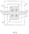
- a transistor cell in accordance with this embodiment is shown in top view in Figure 4, and has a similar structure to that shown in Figure 2, except that multiple P+ clamping regions 40a, 40b, 40c, 40d are provided in gate region 46, and only two bridges 46a, 46b are provided. N+ regions 44a, 44b and P+ body regions 48a, 48b enclose the cell, which is an elongated rectangle in shape.
- the transistor is for use at a 600 volt typical ordinary operating level. Such a device rated at 600 volts typically would have an actual breakdown in excess of 700 volts to provide a safe operating margin.
- the typical dimensions for one cell for such a device are described hereinafter with reference to Figure 2.
- the spacing between the P+ type diffusions 40 and 44b, that is the width of the cell 42, is typically 15 microns to 20 microns. This spacing is an edge of the voltage clamp region 40 to the nearest edge of the N+ type regions 44a or 44b. This distance is the spacing when the P+ type diffusions are masked during fabrication. The actual spacing when the device is completed will typically be less due to the lateral diffusion effect when the device is fabricated.
- the typical width of the P+ type clamping region 40 is about 10 microns. This width is defined to accommodate a minimum sized electrical contact to the P+ type clamping region 40.
- the width of the cell 42 is typically about 30 to 40 microns. This includes the N+ type region 44a, the gate region 46, the P+ type region 40 and the other N+ type region 44b as defined when the diffusions are masked. In other embodiments which use for instance circular, or hexagonal shaped cells, the dimensions are preferably approximately the same.
- the polysilicon bridges 46a, 46b, 46c are each preferably about 7 microns wide (i.e., the dimension of bridge 46a in a direction perpendicular to line X-X). In a typical power transistor device there are approximately 10,000 such cells 42 to switch a current of about 50 amps.
- the safe operating area curve for the above described IGBT device is as shown in Figure 5 which shows collector-emitter current I CE plotted against collector-emitter voltage V CE .
- the maximum current is at I 1 .
- the SOA I of the IGBT embodiment of the present invention (solid line) lies within the SOA WB of a prior art wide base PNP transistor.
- the SOA I of the present invention is generally superior, as shown, to the SOA P of a prior art IGBT (dotted line).
- the breakdown voltage of one embodiment of the present invention is at about 750 volts, which corresponds to the avalanche voltage V A of a prior art wide base PNP transistor.
- a wide base PNP transistor has an SOA WB (interrupted line) approaching the ideal; however, such a structure as is well known is not suitable for a power transistor.
- the SOA for the transistor cell in accordance with the IGBT embodiment of the present invention is effectively a combination of the SOA of a bipolar transistor and the SOA of the active device of each cell.
- the transistor in accordance with the invention is formed by conventional masking, implantation, and diffusing processes as is known in the art.
- the process steps in accordance with the invention in the preferred embodiment are as follows for the IGBT device shown in Figure 3A.
- Substrate 60 is preferably silicon having a conductivity of about .005 to .01 ⁇ -cm and a ⁇ 100> crystal orientation, but semiconductor materials other than silicon having other conductance, conductivity type, and crystal orientation are also appropriate.
- Substrate P+ type region 60 is conventionally doped to a level of about 5 x 10 18 ions per cm 3 .
- the P+ doping is achieved using boron.
- the substrate N+ doping level is preferably approximately 10 19 ions per cm 3 and is achieved using arsenic or phosphorus.
- the N type region 62 is then grown epitaxially to approximately 5-10 microns thick and provided with a arsenic or phosphorus doping of about 1 x 10 16 to 5 x 10 17 atoms per cm 3 .
- Grown conventionally on top of the N type region is the N- type epitaxial layer 64, which is grown to approximately 60 microns thick.
- the doping level of the epitaxial layer 64 is about 1 x 10 14 per cm 3 .
- Field oxide layer 140 is conventionally grown over epitaxial layer 69.
- field oxide layer 140 is conventionally patterned using photoresist. In areas exposed by the mask, field oxide 140 is removed to form openings for passage of impurities for formation of P+ regions 48a, 40.
- P+ type deep body region 48a and clamping region 40 are conventionally formed, preferably in one step. This is done preferably by subjecting the wafer to an ion implantation process using boron, a dosage of about 10 16 ions per cm 2 , and an implant energy of about 120 KeV.
- regions 48a, 40 are formed by a boron nitride injection which is used as a P+ diffusion source. The wafer is then subjected to a diffusing process. Regions 48a and 40 preferably are each about 3 to 6 microns deep and have a doping level of about 5 x 10 19 to 10 20 atoms/cm 3 . Then a layer of silicon dioxide 142 about 500 nm in thickness is regrown over the openings in field oxide layer 140.
- a second mask is used to conventionally pattern and remove portions of field oxide 140 and regrown oxide 142, leaving portions 144 of the two combined oxide layers 140, 142 over P+ regions 48a, 40, and also over the high voltage termination regions at the edge (not shown) of each die of the wafer.
- Silicon dioxide layer 74 (see Figure 6d) is formed on epitaxial layer 64. Silicon dioxide layer 74 is thermally grown to a thickness of about 100 nm and serves as the gate insulating layer. Polycrystalline silicon layer 46 is the gate layer and is formed over silicon dioxide layer 74 typically by chemical vapor deposition, to a thickness of about 500 nm. Other conductive materials can be used as the gate layer.
- Silicon dioxide layer 74 and polycrystalline silicon layer 46 are then conventionally patterned (see Figure.6e) using a photoresist layer and a third mask (not shown). Then the exposed portions of gate layer 46, and the portions of silicon dioxide layer 74 lying thereunder are removed.
- Figure 8f shows the configuration of a portion of the polysilicon gate layer 46 after patterning in a top view, showing polysilicon gate layer "bridges" 46a, 46b, and 46c respectively to adjacent gate regions 52b, 54b, and 58b of respectively cells 52, 54, and 58, as discussed above in connection with Figure 2.
- Figure 6f illustrates the repetitive pattern of polysilicon gate layer 46 after it is patterned.
- the opening 40b in gate layer 46 is for electrical contact to clamping region 40 in the underlying epitaxial layer (not shown).
- P type body regions 68a, 68b, are formed conventionally by ion implantation using polycrystalline silicon layer 46 as a mask.
- dopants such as boron or aluminum are implanted into the wafer with a dosage of about 10 14 per cm 2 and an implant energy of about 40 to 100 KeV.
- the wafer is then subject to a diffusion process so that regions 68a, 68b, are each about 3 to 4 microns deep and have a surface doping level of about 1 x 10 17 to 10 18 ions per cm 3 .
- a thin silicon dioxide layer (not shown) is thermally grown over the entire wafer surface to a thickness of about 200 nm during the diffusion process.
- the N+ type source regions 78, 44a are then conventionally formed preferably by ion implantation using arsenic or phosphorus at a dosage of about 8 x 10 15 per cm 2 and an implant energy of about 60 KeV.
- the wafer is then subjected to a diffusion process.
- the N+ type regions 78, 44a each preferably are less than one micron deep and have a doping level of about 5 x 10 19 to 10 20 ions per cm 3 .
- polysilicon layer 46 serves as the mask for both the P type body regions 68a, 68b and N+ type source regions 78, 44a.
- a fourth mask (not shown) is used to form an N+ type body region block implant (not shown) at the edge of each die only.
- This block implant prevents the P type body regions from going into the high voltage termination region at the die edge.
- an insulating layer of PSG or BPSG or silicon dioxide or silicon nitride (not shown) is formed over the surface of the transistor.
- This insulating layer is conventionally patterned using a fifth mask, to open contacts to the polysilicon layer 46 and to the various semiconductor regions at the principal surface of the epitaxial layer 64.
- a layer of conductive material such as aluminum is then formed over the wafer and conventionally patterned by a sixth mask (not shown) to provide electrical contacts to the emitter/body regions, the gate layer, and the clamping region.
- a second layer of conductive material is conventionally formed on the backside of the wafer to electrically contact the substrate 60.
- a passivation layer is then conventionally formed (not shown) and openings conventionally formed through the passivation layer by a seventh mask for the bonding pads.
- the intermediate N type layer region 62 shown in Figures 3A and 38 advantageously stops semiconductor depletion to that point and prevents undesirable punch through from the P+ type body region to the top of the substrate layer 60.
- the device would function therefore in an alternative embodiment without the N type layer region 62.
- the epitaxial N- type layer 64 would in this case preferably be almost double the thickness compared to a transistor with the N- type layer 62, 110 included.
- the N type region 62, 110 thus provides the benefit of a thinner epitaxial layer. Note that as is known in the art, depletion starts from the top and extends from the surface towards the substrate. If the N- type layer region 62, 110 is removed, then depletion tends to reach through to the P+ type substrate region 60 of Figure 3A. This may disadvantageously cause injection from the substrate P+ type region 60 in the IGBT device of Figure 3A, which will therefore undesirably cause a low breakdown voltage.
- the invention is applicable to high voltage integrated circuits as well as to discrete power transistors as described above.
- the active portion of each cell is preferably protected through a zener diode clamp in accordance with the invention.
Claims (8)
- Transistor comprenant une pluralité de cellules dans lequel chaque cellule comprend:un corps semiconducteur (64) d'un premier type de conductivité;une première zone sensiblement annulaire (48) d'un deuxième type de conductivité formée dans le corps semiconducteur;une deuxième zone (44) du premier type de conductivité formée dans la zone annulaire; etune zone de grille conductrice (46) recouvrant une surface du corps semiconducteur et dont l'étendue est définie par la partie intérieure de la deuxième zone; caractérisé par:une zone de fixation de niveau (40) du deuxième type de conductivité formée dans la partie intérieure des première et deuxième zones, la zone de fixation de niveau ayant une tension de claquage inférieure à la tension de claquage des autres parties de la cellule, une forme en coupe transversale différente de celle de la première zone annulaire (48), et une profondeur et un niveau de dopage identiques à ceux de la première zone annulaire.
- Transistor selon la revendication 1, dans lequel la zone annulaire (48) et la deuxième zone (44) sont de forme sensiblement carrée dans un plan défini par une surface principale du corps semiconducteur.
- Transistor selon la revendication 1 ou 2, dans lequel la zone de fixation de niveau (40) est de forme sphérique dans un plan perpendiculaire à un plan défini par une surface principale du corps semiconducteur.
- Transistor selon la revendication 1 ou 2, dans lequel le transistor est un transistor bipolaire à grille isolée, et la zone de fixation de niveau (40) et le corps semiconducteur (60,64) forment des parties d'un transistor à jonction bipolaire.
- Transistor selon la revendication 1 ou 2, dans lequel le transistor est un transistor à effet de champ et la zone de fixation de niveau (40) et le corps semiconducteur (64) forment une diode Zener.
- Transistor selon l'une quelconque des revendications précédentes, dans lequel la zone de grille conductrice (40) (sic) comprend une partie étendue qui est la zone de grille conductrice d'une cellule adjacente.
- Transistor selon la revendication 6, dans lequel la zone de grille conductrice d'une première cellule comprend une couche de silicium polycristallin connecté à la zone de grille conductrice d'au moins une cellule attenante par une extension de la couche de silicium polycristallin.
- Procédé de réalisation d'une cellule de transistor comprenant une pluralité de cellules, le procédé comprenant les étapes de:formation dans un corps semiconducteur (64) d'un premier type de conductivité d'une première zone sensiblement annulaire (48) d'un deuxième type de conductivité;formation d'une deuxième zone (44) du premier type de conductivité dans la zone annulaire; etformation d'une zone de grille conductrice (46) recouvrant une surface du corps semiconducteur et dont l'étendue est définie par la partie intérieure de la deuxième zone; caractérisé par la formation d'une zone de fixation de niveau (40) du deuxième type de conductivité dans la partie intérieure des première et deuxième zones, la zone de fixation de niveau ayant une tension de claquage inférieure à la tension de claquage des autres parties de la cellule, une forme en coupe transversale différente de celle de la première zone annulaire (48), et une profondeur et un niveau de dopage identiques à ceux de la première zone annulaire.
Applications Claiming Priority (2)
| Application Number | Priority Date | Filing Date | Title |
|---|---|---|---|
| US40084889A | 1989-08-30 | 1989-08-30 | |
| US400848 | 1989-08-30 |
Publications (3)
| Publication Number | Publication Date |
|---|---|
| EP0416805A2 EP0416805A2 (fr) | 1991-03-13 |
| EP0416805A3 EP0416805A3 (en) | 1991-03-27 |
| EP0416805B1 true EP0416805B1 (fr) | 1996-11-20 |
Family
ID=23585274
Family Applications (1)
| Application Number | Title | Priority Date | Filing Date |
|---|---|---|---|
| EP90309443A Expired - Lifetime EP0416805B1 (fr) | 1989-08-30 | 1990-08-29 | Transistor comportant un limiteur de tension |
Country Status (4)
| Country | Link |
|---|---|
| US (1) | US5136349A (fr) |
| EP (1) | EP0416805B1 (fr) |
| JP (1) | JP3122119B2 (fr) |
| DE (1) | DE69029180T2 (fr) |
Cited By (1)
| Publication number | Priority date | Publication date | Assignee | Title |
|---|---|---|---|---|
| US8254070B2 (en) | 2006-05-15 | 2012-08-28 | Infineon Technologies Ag | Vehicle on-board electric power system |
Families Citing this family (67)
| Publication number | Priority date | Publication date | Assignee | Title |
|---|---|---|---|---|
| JP2862027B2 (ja) * | 1991-03-12 | 1999-02-24 | 株式会社デンソー | 絶縁ゲート型バイポーラトランジスタ |
| GB9115699D0 (en) * | 1991-07-19 | 1991-09-04 | Philips Electronic Associated | An overvoltage protected semiconductor switch |
| DE4127033A1 (de) * | 1991-08-16 | 1993-02-18 | Asea Brown Boveri | Mos-gesteuerter thyristor mct |
| JPH05110085A (ja) * | 1991-10-14 | 1993-04-30 | Mitsubishi Electric Corp | 電界効果型半導体装置およびその製造方法 |
| US5289028A (en) * | 1991-11-04 | 1994-02-22 | Motorola, Inc. | High power semiconductor device with integral on-state voltage detection structure |
| US5243211A (en) * | 1991-11-25 | 1993-09-07 | Harris Corporation | Power fet with shielded channels |
| US5260590A (en) * | 1991-12-23 | 1993-11-09 | Harris Corp. | Field effect transistor controlled thyristor having improved turn-on characteristics |
| JP3111576B2 (ja) * | 1992-01-06 | 2000-11-27 | 富士電機株式会社 | 半導体装置 |
| JPH05206469A (ja) * | 1992-01-29 | 1993-08-13 | Hitachi Ltd | 絶縁ゲート型バイポーラトランジスタ |
| JPH05283702A (ja) * | 1992-04-03 | 1993-10-29 | Hitachi Ltd | 複合制御型半導体装置及びそれを使用した電力変換装置 |
| US5430314A (en) * | 1992-04-23 | 1995-07-04 | Siliconix Incorporated | Power device with buffered gate shield region |
| JP3081739B2 (ja) * | 1992-10-20 | 2000-08-28 | 三菱電機株式会社 | 絶縁ゲート型半導体装置及びその製造方法 |
| FR2698486B1 (fr) * | 1992-11-24 | 1995-03-10 | Sgs Thomson Microelectronics | Structure de protection contre les surtensions directes pour composant semiconducteur vertical. |
| DE4244272A1 (de) * | 1992-12-28 | 1994-06-30 | Daimler Benz Ag | Feldeffektgesteuertes Halbleiterbauelement |
| US5719412A (en) * | 1993-04-02 | 1998-02-17 | Nippondenso Co., Ltd | Insulated gate bipolar transistor |
| DE4313170A1 (de) * | 1993-04-22 | 1994-10-27 | Abb Management Ag | Leistungshalbleiterbauelement |
| JP3216743B2 (ja) * | 1993-04-22 | 2001-10-09 | 富士電機株式会社 | トランジスタ用保護ダイオード |
| EP0661755A1 (fr) * | 1993-12-28 | 1995-07-05 | AT&T Corp. | Dispositif semi-conducteur haute-tension avec une robustesse électrique améliorée et un espacement cellulaire réduit |
| US5723882A (en) * | 1994-03-10 | 1998-03-03 | Nippondenso Co., Ltd. | Insulated gate field effect transistor having guard ring regions |
| JP2962136B2 (ja) * | 1994-03-16 | 1999-10-12 | 株式会社日立製作所 | 絶縁ゲート型半導体装置及びそれを用いた電力変換装置 |
| US5689129A (en) * | 1995-06-07 | 1997-11-18 | Harris Corporation | High efficiency power MOS switch |
| KR0159073B1 (ko) * | 1995-10-16 | 1998-12-01 | 김광호 | 트렌치 dmos 트랜지스터와 그의 제조방법 |
| KR100206555B1 (ko) * | 1995-12-30 | 1999-07-01 | 윤종용 | 전력용 트랜지스터 |
| US5844277A (en) * | 1996-02-20 | 1998-12-01 | Magepower Semiconductor Corp. | Power MOSFETs and cell topology |
| US5723916A (en) * | 1996-05-17 | 1998-03-03 | Delco Electronics Corporation | Electrical load driving device including load current limiting circuitry |
| EP0865085A1 (fr) * | 1997-03-11 | 1998-09-16 | STMicroelectronics S.r.l. | Transistor bipolaire à grille isolée avec une grande robustesse dynamique |
| KR100256109B1 (ko) * | 1997-05-07 | 2000-05-01 | 김덕중 | 전력 반도체 장치 |
| EP0893821A1 (fr) * | 1997-07-21 | 1999-01-27 | STMicroelectronics S.r.l. | Procédé de fabrication d'un transistor en technlogie DMOS utilisant une seule étape de traitement thermique pour la formation des régions de source et de corps |
| DE19738324C1 (de) * | 1997-09-02 | 1998-09-03 | Siemens Ag | DMOS mit großer Kanalweite und hoher Avalanche-Festigkeit |
| US6121089A (en) * | 1997-10-17 | 2000-09-19 | Intersil Corporation | Methods of forming power semiconductor devices having merged split-well body regions therein |
| US6005271A (en) * | 1997-11-05 | 1999-12-21 | Magepower Semiconductor Corp. | Semiconductor cell array with high packing density |
| IT1296832B1 (it) * | 1997-12-02 | 1999-08-02 | Sgs Thomson Microelectronics | Struttura integrata di protezione con dispositivi a soglia di conduzione inversa prestabilita di polarizzazione |
| JP3817380B2 (ja) * | 1999-01-14 | 2006-09-06 | ローム株式会社 | 絶縁ゲート型半導体装置 |
| JP4681176B2 (ja) * | 1999-07-15 | 2011-05-11 | ローム株式会社 | Mos型電界効果トランジスタを有する半導体装置 |
| GB2354879B (en) * | 1999-08-11 | 2004-05-12 | Mitel Semiconductor Ltd | A semiconductor device |
| JP4568929B2 (ja) * | 1999-09-21 | 2010-10-27 | 株式会社デンソー | 炭化珪素半導体装置及びその製造方法 |
| US6482681B1 (en) | 2000-05-05 | 2002-11-19 | International Rectifier Corporation | Hydrogen implant for buffer zone of punch-through non epi IGBT |
| US6242288B1 (en) * | 2000-05-05 | 2001-06-05 | International Rectifier Corp. | Anneal-free process for forming weak collector |
| JP3727827B2 (ja) * | 2000-05-15 | 2005-12-21 | 株式会社東芝 | 半導体装置 |
| DE10205324B4 (de) * | 2001-02-09 | 2012-04-19 | Fuji Electric Co., Ltd. | Halbleiterbauelement |
| US6566710B1 (en) * | 2001-08-29 | 2003-05-20 | National Semiconductor Corporation | Power MOSFET cell with a crossed bar shaped body contact area |
| US6791161B2 (en) * | 2002-04-08 | 2004-09-14 | Fabtech, Inc. | Precision Zener diodes |
| JP2004079988A (ja) * | 2002-06-19 | 2004-03-11 | Toshiba Corp | 半導体装置 |
| TW578306B (en) * | 2002-11-07 | 2004-03-01 | Mosel Vitelic Inc | Power metal oxide semiconductor field effect transistor layout structure |
| US6858887B1 (en) * | 2003-07-30 | 2005-02-22 | Innovative Technology Licensing Llc | BJT device configuration and fabrication method with reduced emitter width |
| US7274076B2 (en) * | 2003-10-20 | 2007-09-25 | Micron Technology, Inc. | Threshold voltage adjustment for long channel transistors |
| US7279743B2 (en) | 2003-12-02 | 2007-10-09 | Vishay-Siliconix | Closed cell trench metal-oxide-semiconductor field effect transistor |
| US8183629B2 (en) * | 2004-05-13 | 2012-05-22 | Vishay-Siliconix | Stacked trench metal-oxide-semiconductor field effect transistor device |
| US8471390B2 (en) * | 2006-05-12 | 2013-06-25 | Vishay-Siliconix | Power MOSFET contact metallization |
| US8368126B2 (en) * | 2007-04-19 | 2013-02-05 | Vishay-Siliconix | Trench metal oxide semiconductor with recessed trench material and remote contacts |
| US7687825B2 (en) * | 2007-09-18 | 2010-03-30 | Cree, Inc. | Insulated gate bipolar conduction transistors (IBCTS) and related methods of fabrication |
| CN102574977B (zh) | 2009-09-30 | 2013-12-11 | 旭硝子株式会社 | 异氰酸酯基末端预聚物的制造方法以及由此获得的预聚物及聚氨酯树脂 |
| US9306056B2 (en) | 2009-10-30 | 2016-04-05 | Vishay-Siliconix | Semiconductor device with trench-like feed-throughs |
| US8134205B2 (en) * | 2010-01-06 | 2012-03-13 | Ptek Technology Co., Ltd. | Layout structure of power MOS transistor |
| KR101130019B1 (ko) | 2010-09-09 | 2012-03-26 | 주식회사 케이이씨 | 전력용 반도체 디바이스 |
| US10115815B2 (en) | 2012-12-28 | 2018-10-30 | Cree, Inc. | Transistor structures having a deep recessed P+ junction and methods for making same |
| US9530844B2 (en) * | 2012-12-28 | 2016-12-27 | Cree, Inc. | Transistor structures having reduced electrical field at the gate oxide and methods for making same |
| US20150311325A1 (en) * | 2014-04-23 | 2015-10-29 | Cree, Inc. | Igbt structure on sic for high performance |
| CN107785366B (zh) * | 2016-08-31 | 2020-04-14 | 无锡华润上华科技有限公司 | 集成有结型场效应晶体管的器件及其制造方法 |
| KR102394547B1 (ko) * | 2017-10-25 | 2022-05-04 | 현대자동차 주식회사 | 반도체 소자 |
| US10615274B2 (en) | 2017-12-21 | 2020-04-07 | Cree, Inc. | Vertical semiconductor device with improved ruggedness |
| US11489069B2 (en) | 2017-12-21 | 2022-11-01 | Wolfspeed, Inc. | Vertical semiconductor device with improved ruggedness |
| US11637192B2 (en) | 2020-06-24 | 2023-04-25 | Electronics And Telecommunications Research Institute | Metal oxide semiconductor-controlled thyristor device having uniform turn-off characteristic and method of manufacturing the same |
| KR102509083B1 (ko) * | 2020-06-24 | 2023-03-14 | 한국전자통신연구원 | 균일한 턴-오프 특성을 갖는 mct 소자 및 그 제조 방법 |
| CN112820769A (zh) * | 2020-12-31 | 2021-05-18 | 全球能源互联网研究院有限公司 | 一种碳化硅mosfet器件及其制备方法 |
| CN114678277B (zh) * | 2022-05-27 | 2022-08-16 | 深圳平创半导体有限公司 | 中心注入p+屏蔽区的分裂栅平面mosfet及其制造方法 |
| CN116190422A (zh) * | 2023-04-25 | 2023-05-30 | 深圳平创半导体有限公司 | 一种八边形分裂栅平面碳化硅mosfet版图结构 |
Family Cites Families (16)
| Publication number | Priority date | Publication date | Assignee | Title |
|---|---|---|---|---|
| JPS57206073A (en) * | 1981-06-12 | 1982-12-17 | Hitachi Ltd | Mis semiconductor device |
| NL8302092A (nl) * | 1983-06-13 | 1985-01-02 | Philips Nv | Halfgeleiderinrichting bevattende een veldeffekttransistor. |
| JPH0612828B2 (ja) * | 1983-06-30 | 1994-02-16 | 株式会社東芝 | 半導体装置 |
| US4837606A (en) * | 1984-02-22 | 1989-06-06 | General Electric Company | Vertical MOSFET with reduced bipolar effects |
| JPS60196974A (ja) * | 1984-03-19 | 1985-10-05 | Toshiba Corp | 導電変調型mosfet |
| GB2165090A (en) * | 1984-09-26 | 1986-04-03 | Philips Electronic Associated | Improving the field distribution in high voltage semiconductor devices |
| JPS61182264A (ja) * | 1985-02-08 | 1986-08-14 | Nissan Motor Co Ltd | 縦型mosトランジスタ |
| JPS6239069A (ja) * | 1985-08-13 | 1987-02-20 | Mitsubishi Electric Corp | 電界効果型半導体装置 |
| EP0219995B1 (fr) * | 1985-09-30 | 1994-03-02 | Kabushiki Kaisha Toshiba | Thyristor à commande d'extinction comportant des transistors d'allumage/extinction indépendants |
| US4779123A (en) * | 1985-12-13 | 1988-10-18 | Siliconix Incorporated | Insulated gate transistor array |
| IT1204243B (it) * | 1986-03-06 | 1989-03-01 | Sgs Microelettronica Spa | Procedimento autoallineato per la fabbricazione di celle dmos di piccole dimensioni e dispositivi mos ottenuti mediante detto procedimento |
| IT1213411B (it) * | 1986-12-17 | 1989-12-20 | Sgs Microelettronica Spa | Struttura mos di potenza con dispositivo di protezione contro le sovratensioni e processo per lasua fabbricazione. |
| JPS64769A (en) * | 1987-02-16 | 1989-01-05 | Nec Corp | Vertical field-effect transistor |
| US4775879A (en) * | 1987-03-18 | 1988-10-04 | Motorola Inc. | FET structure arrangement having low on resistance |
| US4823176A (en) * | 1987-04-03 | 1989-04-18 | General Electric Company | Vertical double diffused metal oxide semiconductor (VDMOS) device including high voltage junction exhibiting increased safe operating area |
| JPS63252480A (ja) * | 1987-04-09 | 1988-10-19 | Mitsubishi Electric Corp | 縦形モス電界効果トランジスタ |
-
1990
- 1990-08-29 EP EP90309443A patent/EP0416805B1/fr not_active Expired - Lifetime
- 1990-08-29 DE DE69029180T patent/DE69029180T2/de not_active Expired - Fee Related
- 1990-08-30 JP JP02226839A patent/JP3122119B2/ja not_active Expired - Fee Related
- 1990-10-12 US US07/597,118 patent/US5136349A/en not_active Expired - Lifetime
Cited By (1)
| Publication number | Priority date | Publication date | Assignee | Title |
|---|---|---|---|---|
| US8254070B2 (en) | 2006-05-15 | 2012-08-28 | Infineon Technologies Ag | Vehicle on-board electric power system |
Also Published As
| Publication number | Publication date |
|---|---|
| US5136349A (en) | 1992-08-04 |
| JPH03142972A (ja) | 1991-06-18 |
| DE69029180D1 (de) | 1997-01-02 |
| JP3122119B2 (ja) | 2001-01-09 |
| DE69029180T2 (de) | 1997-05-22 |
| EP0416805A2 (fr) | 1991-03-13 |
| EP0416805A3 (en) | 1991-03-27 |
Similar Documents
| Publication | Publication Date | Title |
|---|---|---|
| EP0416805B1 (fr) | Transistor comportant un limiteur de tension | |
| KR100256903B1 (ko) | 전계효과 트랜지스터 | |
| US5698454A (en) | Method of making a reverse blocking IGBT | |
| US5527720A (en) | Method of forming a semiconductor device having a vertical insulated gate FET and a breakdown region remote from the gate | |
| JP2988871B2 (ja) | トレンチゲートパワーmosfet | |
| JP4210110B2 (ja) | 半導体装置 | |
| US5557127A (en) | Termination structure for mosgated device with reduced mask count and process for its manufacture | |
| US5342797A (en) | Method for forming a vertical power MOSFET having doped oxide side wall spacers | |
| US6306728B1 (en) | Stable high voltage semiconductor device structure | |
| US5701023A (en) | Insulated gate semiconductor device typically having subsurface-peaked portion of body region for improved ruggedness | |
| US5382536A (en) | Method of fabricating lateral DMOS structure | |
| US5798549A (en) | Conductive layer overlaid self-aligned MOS-gated semiconductor devices | |
| US5486718A (en) | High voltage planar edge termination structure and method of making same | |
| EP2093802A1 (fr) | Tec à grille isolante et son procédé de fabrication | |
| KR20040030836A (ko) | 반도체 장치의 제조 방법 및 셀룰러 쇼트키 정류기 | |
| US4929991A (en) | Rugged lateral DMOS transistor structure | |
| JP2000508122A (ja) | 半導体デバイス | |
| US5124764A (en) | Symmetric vertical MOS transistor with improved high voltage operation | |
| US6030870A (en) | High density MOS technology power device | |
| US6104060A (en) | Cost savings for manufacturing planar MOSFET devices achieved by implementing an improved device structure and fabrication process eliminating passivation layer and/or field plate | |
| US5731611A (en) | MOSFET transistor cell manufactured with selectively implanted punch through prevent and threshold reductoin zones | |
| US5912491A (en) | MOS device | |
| US5831318A (en) | Radhard mosfet with thick gate oxide and deep channel region | |
| JP2808871B2 (ja) | Mos型半導体素子の製造方法 | |
| JPH03205832A (ja) | 絶縁ゲート形半導体装置とその製造方法 |
Legal Events
| Date | Code | Title | Description |
|---|---|---|---|
| PUAI | Public reference made under article 153(3) epc to a published international application that has entered the european phase |
Free format text: ORIGINAL CODE: 0009012 |
|
| PUAL | Search report despatched |
Free format text: ORIGINAL CODE: 0009013 |
|
| AK | Designated contracting states |
Kind code of ref document: A2 Designated state(s): DE IT NL |
|
| AK | Designated contracting states |
Kind code of ref document: A3 Designated state(s): DE IT NL |
|
| RIN1 | Information on inventor provided before grant (corrected) |
Inventor name: BENCUYA, IZAK Inventor name: YILMAZ, HAMZA |
|
| 17P | Request for examination filed |
Effective date: 19910926 |
|
| 17Q | First examination report despatched |
Effective date: 19931014 |
|
| GRAH | Despatch of communication of intention to grant a patent |
Free format text: ORIGINAL CODE: EPIDOS IGRA |
|
| GRAH | Despatch of communication of intention to grant a patent |
Free format text: ORIGINAL CODE: EPIDOS IGRA |
|
| GRAA | (expected) grant |
Free format text: ORIGINAL CODE: 0009210 |
|
| ITF | It: translation for a ep patent filed |
Owner name: DE DOMINICIS & MAYER S.R.L. |
|
| AK | Designated contracting states |
Kind code of ref document: B1 Designated state(s): DE IT NL |
|
| REF | Corresponds to: |
Ref document number: 69029180 Country of ref document: DE Date of ref document: 19970102 |
|
| PLBE | No opposition filed within time limit |
Free format text: ORIGINAL CODE: 0009261 |
|
| STAA | Information on the status of an ep patent application or granted ep patent |
Free format text: STATUS: NO OPPOSITION FILED WITHIN TIME LIMIT |
|
| 26N | No opposition filed | ||
| PGFP | Annual fee paid to national office [announced via postgrant information from national office to epo] |
Ref country code: NL Payment date: 20030801 Year of fee payment: 14 |
|
| PGFP | Annual fee paid to national office [announced via postgrant information from national office to epo] |
Ref country code: DE Payment date: 20030930 Year of fee payment: 14 |
|
| PG25 | Lapsed in a contracting state [announced via postgrant information from national office to epo] |
Ref country code: NL Free format text: LAPSE BECAUSE OF NON-PAYMENT OF DUE FEES Effective date: 20050301 Ref country code: DE Free format text: LAPSE BECAUSE OF NON-PAYMENT OF DUE FEES Effective date: 20050301 |
|
| NLV4 | Nl: lapsed or anulled due to non-payment of the annual fee |
Effective date: 20050301 |
|
| PG25 | Lapsed in a contracting state [announced via postgrant information from national office to epo] |
Ref country code: IT Free format text: LAPSE BECAUSE OF NON-PAYMENT OF DUE FEES Effective date: 20050829 |