EP0401635A2 - Procédé de fabrication d'un capteur à éléments résistifs - Google Patents
Procédé de fabrication d'un capteur à éléments résistifs Download PDFInfo
- Publication number
- EP0401635A2 EP0401635A2 EP90110066A EP90110066A EP0401635A2 EP 0401635 A2 EP0401635 A2 EP 0401635A2 EP 90110066 A EP90110066 A EP 90110066A EP 90110066 A EP90110066 A EP 90110066A EP 0401635 A2 EP0401635 A2 EP 0401635A2
- Authority
- EP
- European Patent Office
- Prior art keywords
- substrate
- region
- working
- unit
- sensor
- Prior art date
- Legal status (The legal status is an assumption and is not a legal conclusion. Google has not performed a legal analysis and makes no representation as to the accuracy of the status listed.)
- Granted
Links
Images


Classifications
-
- G—PHYSICS
- G01—MEASURING; TESTING
- G01L—MEASURING FORCE, STRESS, TORQUE, WORK, MECHANICAL POWER, MECHANICAL EFFICIENCY, OR FLUID PRESSURE
- G01L9/00—Measuring steady of quasi-steady pressure of fluid or fluent solid material by electric or magnetic pressure-sensitive elements; Transmitting or indicating the displacement of mechanical pressure-sensitive elements, used to measure the steady or quasi-steady pressure of a fluid or fluent solid material, by electric or magnetic means
- G01L9/0041—Transmitting or indicating the displacement of flexible diaphragms
- G01L9/0042—Constructional details associated with semiconductive diaphragm sensors, e.g. etching, or constructional details of non-semiconductive diaphragms
-
- G—PHYSICS
- G01—MEASURING; TESTING
- G01L—MEASURING FORCE, STRESS, TORQUE, WORK, MECHANICAL POWER, MECHANICAL EFFICIENCY, OR FLUID PRESSURE
- G01L19/00—Details of, or accessories for, apparatus for measuring steady or quasi-steady pressure of a fluent medium insofar as such details or accessories are not special to particular types of pressure gauges
- G01L19/14—Housings
- G01L19/147—Details about the mounting of the sensor to support or covering means
-
- G—PHYSICS
- G01—MEASURING; TESTING
- G01P—MEASURING LINEAR OR ANGULAR SPEED, ACCELERATION, DECELERATION, OR SHOCK; INDICATING PRESENCE, ABSENCE, OR DIRECTION, OF MOVEMENT
- G01P15/00—Measuring acceleration; Measuring deceleration; Measuring shock, i.e. sudden change of acceleration
- G01P15/02—Measuring acceleration; Measuring deceleration; Measuring shock, i.e. sudden change of acceleration by making use of inertia forces using solid seismic masses
- G01P15/08—Measuring acceleration; Measuring deceleration; Measuring shock, i.e. sudden change of acceleration by making use of inertia forces using solid seismic masses with conversion into electric or magnetic values
- G01P15/12—Measuring acceleration; Measuring deceleration; Measuring shock, i.e. sudden change of acceleration by making use of inertia forces using solid seismic masses with conversion into electric or magnetic values by alteration of electrical resistance
- G01P15/123—Measuring acceleration; Measuring deceleration; Measuring shock, i.e. sudden change of acceleration by making use of inertia forces using solid seismic masses with conversion into electric or magnetic values by alteration of electrical resistance by piezo-resistive elements, e.g. semiconductor strain gauges
-
- G—PHYSICS
- G01—MEASURING; TESTING
- G01P—MEASURING LINEAR OR ANGULAR SPEED, ACCELERATION, DECELERATION, OR SHOCK; INDICATING PRESENCE, ABSENCE, OR DIRECTION, OF MOVEMENT
- G01P15/00—Measuring acceleration; Measuring deceleration; Measuring shock, i.e. sudden change of acceleration
- G01P15/02—Measuring acceleration; Measuring deceleration; Measuring shock, i.e. sudden change of acceleration by making use of inertia forces using solid seismic masses
- G01P15/08—Measuring acceleration; Measuring deceleration; Measuring shock, i.e. sudden change of acceleration by making use of inertia forces using solid seismic masses with conversion into electric or magnetic values
- G01P2015/0805—Measuring acceleration; Measuring deceleration; Measuring shock, i.e. sudden change of acceleration by making use of inertia forces using solid seismic masses with conversion into electric or magnetic values being provided with a particular type of spring-mass-system for defining the displacement of a seismic mass due to an external acceleration
- G01P2015/0822—Measuring acceleration; Measuring deceleration; Measuring shock, i.e. sudden change of acceleration by making use of inertia forces using solid seismic masses with conversion into electric or magnetic values being provided with a particular type of spring-mass-system for defining the displacement of a seismic mass due to an external acceleration for defining out-of-plane movement of the mass
- G01P2015/084—Measuring acceleration; Measuring deceleration; Measuring shock, i.e. sudden change of acceleration by making use of inertia forces using solid seismic masses with conversion into electric or magnetic values being provided with a particular type of spring-mass-system for defining the displacement of a seismic mass due to an external acceleration for defining out-of-plane movement of the mass the mass being suspended at more than one of its sides, e.g. membrane-type suspension, so as to permit multi-axis movement of the mass
-
- Y—GENERAL TAGGING OF NEW TECHNOLOGICAL DEVELOPMENTS; GENERAL TAGGING OF CROSS-SECTIONAL TECHNOLOGIES SPANNING OVER SEVERAL SECTIONS OF THE IPC; TECHNICAL SUBJECTS COVERED BY FORMER USPC CROSS-REFERENCE ART COLLECTIONS [XRACs] AND DIGESTS
- Y10—TECHNICAL SUBJECTS COVERED BY FORMER USPC
- Y10T—TECHNICAL SUBJECTS COVERED BY FORMER US CLASSIFICATION
- Y10T29/00—Metal working
- Y10T29/49—Method of mechanical manufacture
- Y10T29/49002—Electrical device making
- Y10T29/49082—Resistor making
- Y10T29/49103—Strain gauge making
-
- Y—GENERAL TAGGING OF NEW TECHNOLOGICAL DEVELOPMENTS; GENERAL TAGGING OF CROSS-SECTIONAL TECHNOLOGIES SPANNING OVER SEVERAL SECTIONS OF THE IPC; TECHNICAL SUBJECTS COVERED BY FORMER USPC CROSS-REFERENCE ART COLLECTIONS [XRACs] AND DIGESTS
- Y10—TECHNICAL SUBJECTS COVERED BY FORMER USPC
- Y10T—TECHNICAL SUBJECTS COVERED BY FORMER US CLASSIFICATION
- Y10T29/00—Metal working
- Y10T29/49—Method of mechanical manufacture
- Y10T29/49789—Obtaining plural product pieces from unitary workpiece
Definitions
- This invention relates to a method of manufacturing a sensor using resistance elements and, more particularly, to a method of manufacturing a sensor for detecting, as changes in electric resistance, a mechanical deformation applied to resistance elements formed on a semiconductor substrate.
- an impurity diffusion process, etc. is implemented to a semiconductor wafer to form a large number of resistance elements at respective predetermined positions. Also many chemical or physical processes are implemented to form grooves for rendering flexibility, and to form wiring layers.
- the semiconductor wafer is then cut into a plurality of semiconductor pellets by dicing process. Each pellet serves as a main unit of a single independent force sensor. Thereafter, a weight body is connected to a working portion of the pellet in the case of manufacturing an acceleration sensor, and a magnetic body is connected thereto in place of the weight body in the case of manufacturing a magnetic sensor. Finally, this pellet is accommodated into a package and is then subjected to wire bonding. Thus, a chip is completed as a sensor unit.
- the conventional manufacturing method at the stage for processing a semiconductor wafer, processing can be implemented at the same time to a plurality of sensor units formed on a single wafer.
- weight bodies are required to be connected every units in the case of the acceleration sensor
- magnetic bodies are required to be connected every units in the case of the magnetic sensor.
- pedestals for supporting respective pellets must be connected every units.
- control members for allowing the weight body or the magnetic body not to move exceeding an allowed range in order to prevent the semiconductor substrate from being mechanically broken when a large force is applied to the weight body or the magnetic body.
- the conventional manufacturing method has many process steps which should be processed every pellet, resulting in a poor efficiency and a lowered productivity. Namely, the conventional method has the problem that it is not suitable for mass production, resulting in an increased cost of products.
- an object of this invention is to provide a manufacturing method capable of efficiently mass-producing sensors using resistance element.
- a first embodiment of the invention resides in a method of manufacturing a sensor using resistance elements, comprising: a step of defining, on a first substrate, a working , fixed region, and a flexible region positioned therebetween, a step of forming a resistance element within the flexible region of a first surface of the first substrate, a step of partially removing said first substrate in order to allow the flexible region to have flexibility, a step of connecting a second substrate to a second surface of the first substrate, and a step of cutting the second substrate to thereby form a working body connected to the working region of the first substrate and constituted by a portion of the second substrate, and a pedestal connected to the fixed region of the first substrate and constituted by a portion of the second substrate.
- a second embodiment of the invention of this application resides in a method of manufacturing a sensor using resistance elements, comprising: a step of defining a plurality of unit regions on a first substrate, and defining, within each unit region, a working region, a fixed region, and a flexible region positioned therebetween, a step of forming resistance elements within respective flexible regions on a first surface of the first substrate, a step of partially removing the first substrate in order to allow the respective flexible regions to have flexibility, a step of connecting a second substrate to a second surface of said first substrate, a step of cutting said second substrate to thereby form, within each unit region, a working body connected to the working region of the first substrate and constituted by a portion of the second substrate, and a pedestal connected to the fixed region of the first substrate and constituted by a portion of the second substrate, and a step of cuting off the first and second substrates every unit regions to form independent sensors, respectively.
- a third embodiment of the invention of this application is characterized in that, in the above-mentioned second embodiment of the invention, before the substrate is cut off every unit regions, a groove such that the working body can move therein with a predetermined degree of freedom is further formed on the side of a first surface of a third substrate thereafter to implement a step of connecting the first surface of the third substrate to the second surface of the second substrate and a step of cutting off these first, second and third substrates every unit regions, thus to form sensors, respectively.
- a fourth embodiment of the invention of this application is characterized in that, in the above-mentioned second embodiment of the invention, before the substrate is cut off every unit regions, a groove such that the working portion of the first substrate can move therein with a predetermined degree of freedom is further formed on the side of a first surface of a third substrate thereafter to implement a step of connecting the first surface of the third substrate to the first surface of the first substrate and a step of cutting off these first, second and third substrate every unit regions, thus to form sensors, respectively.
- a fifth embodiment of the invention of this application is characterized in that, in the above-mentioned second embodiment of the invention, resistance elements are formed so as to enable detection of a force exerted on each working region with respect to at least two axis directions of three axis directions of a first axis and a second axis included in a plane defining the first surface of the first substrate and perpendicular to each other, and a third axis perpendicular to the first axis and the second axis.
- a weight body or a magnetic body is formed by a portion of a second substrate, and a pedestal for supporting a first substrate is formed by another portion of the second substrate.
- the weight body, the magnetic body and the pedestal can be formed using a wafer as a unit.
- a control member for limiting a downward movement of the weight body or the magnetic body can be formed by a third substrate.
- a control member for limiting an upward movement of the working portion of the first substrate can be formed by the third substrate.
- movement of the working body can be two-dimensionally or three-dimensionally grasped.
- a sensor for making a three-dimensional detection can be realized.
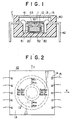
- FIG. 1 is a structual cross section showing an example of an acceleration sensor.
- This sensor includes a semiconductor pellet serving as a main unit.
- the top view of this semiconductor pellet 10 is shown in FIG. 2.
- the cross section of the semiconductor pellet 10 shown at the central portion of FIG. 1 corresponds to the cross section cut along the X-axis of FIG. 2.
- This semiconductor pellet 10 is divided into three regions of a working portion 11, a flexible portion 12, and a fixed portion 13 in order from the inside toward the outside.
- an annular groove is formed on the side of the lower surface of the flexible portion 12. By the presence of this groove, the flexible portion 12 virtually becomes thin in thickness, whereby this portion 12 is caused to have flexibility.
- resistance elements Rx1 to Rx4, Ry1 to Ry4 and Rz1 to Rz4 are formed in predetermined directions, respectively.
- a weight body 20 is connected to the lower part of the working portion 11 and a pedestal 30 is connected to the lower part of the fixed portion 13.
- the bottom surface of the pedestal 30 is connected to the inside bottom surface of a package 40.
- the semiconductor pellet and the weight body 20 are supported by the pedestal 30.
- the weight body 20 is hanging down within the package 40.
- a cover 41 is fitted into the package 40.
- bonding pads 14 shown in FIG. 2 provided on the semiconductor pellet 10 are electrically connected to respective resistance elements within the pellet. These bonding pads 14 and leads 42 provided on the side portions of the package 40 are connected by means of bonding wires
- the above-mentioned detection method is not the gist of this invention, its explanation is omitted here.
- the above-described sensor is constructed as an acceleration sensor, but when there is a need to use the above-described sensor as a magnetic sensor, such a magnetic sensor may be constituted by using a magnetic body in place of the weight body 20.
- control members 51, 52 and 53 are provided in the sensor shown in FIG. 1.
- the control member 51 serves to effect a control such that a displacement in the lateral direction of the weight body 20 does not exceed an allowed value.
- the control member 52 serves to effect a control such that a displacement in a downward direction of the weight body 20 does not exceed an allowed value.
- the control member 53 serves to effect a control such that a displacement in an upward direction of the weight body 20 (the working portion 11 in a direct sense) does not exceed an allowed value.
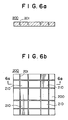
- FIG. 3a shows a plurality of unit regions formed on a semiconductor wafer 100.
- a hatched portion represents one unit region. These unit regions are square, respectively.
- a large number of unit regions are formed on a disk-shaped semiconductor wafer.
- FIGS. 5a and 5b processing of the semiconductor wafer 100 of e.g., silicon, etc. is first carried out. Since this semiconductor wafer 100 is square and is divided into four unit regions for convenience of explanation as described above, completely the same processing is implemented to these four unit regions.
- FIG. 5b is a bottom view of the semiconductor wafer 100 to which processing has been implemented
- FIG. 5a is a side cross sectional view showing the state where the processed semiconductor wafer is cut along the cutting line 5a-5a.
- a plurality of resistance elements R are formed at predetermined positions, respectively.
- each groove 101 is formed circular as shown in FIG. 5b.
- Such an annular groove may be formed by a mechanical processing, an isotropic etching process, or a combination of isotropic and anisotropic etching.
- the anisotropic etching process is ordinarily used.
- a groove formed is not annular, but polygonal (the shape depends upon Miller indices of the semiconductor wafer 100).
- each groove 101 thus formed serves as a working portion 110, the outside portion thereof serves as a fixed portion 130, and the groove portion serves as a flexible portion 120. Accordingly, resistance elements R are just formed on these grooves.
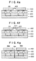
- FIG. 4a shows the state that processing of the semiconductor wafer 100 has been completed.
- an auxiliary substrate 200 as shown in FIGS. 6a and 6b is prepared. Since a portion of the auxiliary substrate 200 finally constitutes a weight body and the remaining portion thereof finally constitutes a pedestal, it is preferable to use a material suitable for a weight body and a pedestal, respectively. In addition, since the auxiliary substrate 200 is connected to the semiconductor wafer 100, it is preferable to use a material having substantially the same coefficient of thermal expansion as that of the semiconductor wafer 100. For example, it is preferable to use a silicon substrate which is the same as the semiconductor wafer 100, or a glass substrate.
- FIG. 6b is a top view of the auxiliary substrate 200 to which processing has been implemented, and FIG.
- FIG. 6a is a side cross sectional view showing the state where the processed auxiliary substrate 200 is cut along the cutting line 6a-6a.
- grooves 201 are longitudinally and laterally formed on the side of the upper surface of the auxiliary substrate 200. The provision of such grooves allow this substrate to be easily subjected to dicing later.
- the positions where grooves 201 are formed may be positions such that portions 210 (four portions in the figure) each corresponding to the working portion 110 of the semiconductor wafer 100 and portions 220 (other portions) each corresponding to the fixed portion 130 are separated from each other.
- this auxiliary substrate 200 is connected to the semiconductor wafer 100 as shown in FIG. 4b. While such a connection may be made by a bonding agent, it is preferable for securely making a connection to use an anodic bonding capable of directly connecting materials to each other. Namely, this method is to apply a voltage across both materials to raise temperatures of the both materials to connect them while applying a force thereto.
- the auxiliary substrate 200 is cut along the grooves 201 by means of a dicing blade.
- Cutting paths 202 are formed on the side opposite to the grooves 201 (the lower part in the figure).
- portions 210 serving as weight bodies
- portions 220 serving as pedestals
- FIG. 6b portions 210 (weight bodies) are positioned at four places. These portions are placed in the state where they are connected only to working portions 110 shown in FIG. 5b. Further, other portions 220 (pedestals) are placed in the state where they are connected only to fixed portions 130 shown in FIG. 5b.
- the flexible portion 120 is in a floating state with respect to the auxiliary substrate 200, it is not connected to any portion.
- the weight body 210 and the pedestal 220 can be formed at the same time.
- the pedestal 220 not only performs a function as a pedestal supporting the fixed portion 130, but also performs a function as a control member to effect a control so that a displacement in a lateral direction of the weight body 210 does not exceed an allowed range (function of the control member 51 in the sensor shown in FIG. 1).
- This allowed range is determined by the width of the cutting path 202 (when the width of the groove 201 is smaller than that of the cutting path 202, the allowed range is determined by the width of the groove 201). It is to be noted that the dicing process implemented here is the dicing process for only the auxiliary substrate 200, and therefore the semiconductor wafer 100 is still in the state of a single wafer.
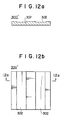
- a control substrate 300 as shown in FIGS. 7a and 7b is then prepared.
- This control substrate 300 serves to control a displacement in a downward direction of the weight body 210 so that it falls within an allowed range.
- a silicon substrate or a glass substrate may be used in the same manner as the auxiliary substrate 200.
- Completely the same processing is implemented to respective four unit regions on the upper surface of the control substrate 300.
- FIG. 7b is a top view of the control substrate 300 to which process has been implemented
- FIG. 7a is a side cross sectional view showing the state where the processed control substrate is cut along the cuting line 7a-7a.
- four square grooves 301 are formed on the side of the upper surface thereof.
- Such grooves 301 serve to control degree of freedom in a downward direction of a displacement of the weight body 210.
- the degree of freedom is determined by depth of the groove 301.
- this control substrate 300 is connected to the auxiliary substrate 200. It is preferable for this connection to use an anodic bonding.
- a control substrate 400 as shown in FIGS. 8a and 8b is then prepared.
- This control substrate 400 serves to control a displacement in an upward direction of the working portion 110 so that it falls within an allowed range.
- a silicon substrate or a glass substrate may be used in the same manner as the auxiliary substrate 200.
- Completely the same processing is implemented to respective four unit regions on the lower surface of the control substrate 400.
- FIG. 8b is a bottom view of the control substrate 400 to which processing has been implemented
- FIG. 8a is a side cross sectional view showing the state where the processed control substrate is cut along the cutting line 8a-8a. On the side of the lower surface thereof, four square grooves 401 are formed.
- Such grooves 401 serve to control the degree of freedom in an upward direction of a displacement of the working portion 110.
- the degree of freedom is determined by depth of the groove 401.
- Another feature of the control substrate 400 resides in that the lateral width is somewhat shorter than those of other substrate, and that a longitudinally elongated groove 402 is formed at the central portion thereof. This is a device for facilitating wire bonding as described later. As shown in FIG. 4e, this control substrate 400 is connected to the upper surface of the semiconductor wafer 100. Also for this connection, it is preferable to use an anodic bonding.
- the upper part of the groove 402 is cut by a cutting path 403. Further, when respective unit regions are cut along cuting path 501 as shown in FIG. 4g, four unit regions shown in FIG. 3b are separated from each other. Thus, sensor main portions 500 are completed.
- the perspective view of the sensor main portion 500 thus completed is shown in FIG. 9.
- the reason why the lateral width of the control substrate 400 is formed short and longitudinally elongated grooves 401 are formed is nothing but aiming at exposing the bonding pads 501 as shown in FIG. 9.
- the sensor main portion 500 obtained as shown in FIG. 9 is accommodated into a package 600 as shown in the side cross sectional view of FIG. 10. Namely, this is accomplished by bonding the bottom portion of the sensor main portion 500 to the inner portion of the package 600. Mounting leads are attached to the package 600. The bonding pads 501 and the inside ends of leads 610 are subjected to bonding by means of bonding wires 620. Thereafter, a cover 630 is fitted over the package 600 and is sealed. An acceleration sensor is thus completed.
- the manufacturing process every pellets after dicing (the above-described manufacturing process II) is very simple as compared to the manufacturing process every wafer (the above-described manufacturing process I). Namely, in accordance with this invention, most of manufacturing steps can be carried out every wafer, and an efficient manufacture suitable for mass production can be made.
Landscapes
- Physics & Mathematics (AREA)
- General Physics & Mathematics (AREA)
- Chemical & Material Sciences (AREA)
- Analytical Chemistry (AREA)
- Pressure Sensors (AREA)
- Force Measurement Appropriate To Specific Purposes (AREA)
Applications Claiming Priority (2)
| Application Number | Priority Date | Filing Date | Title |
|---|---|---|---|
| JP1135539A JP2681215B2 (ja) | 1989-05-29 | 1989-05-29 | 積層基板を用いたセンサの製造方法 |
| JP135539/89 | 1989-05-29 |
Publications (3)
| Publication Number | Publication Date |
|---|---|
| EP0401635A2 true EP0401635A2 (fr) | 1990-12-12 |
| EP0401635A3 EP0401635A3 (fr) | 1992-11-04 |
| EP0401635B1 EP0401635B1 (fr) | 1995-08-02 |
Family
ID=15154148
Family Applications (1)
| Application Number | Title | Priority Date | Filing Date |
|---|---|---|---|
| EP90110066A Expired - Lifetime EP0401635B1 (fr) | 1989-05-29 | 1990-05-28 | Procédé de fabrication d'un capteur à éléments résistifs |
Country Status (4)
| Country | Link |
|---|---|
| US (1) | US5014415A (fr) |
| EP (1) | EP0401635B1 (fr) |
| JP (1) | JP2681215B2 (fr) |
| DE (1) | DE69021280T2 (fr) |
Cited By (4)
| Publication number | Priority date | Publication date | Assignee | Title |
|---|---|---|---|---|
| DE4316279A1 (de) * | 1992-05-15 | 1993-11-18 | Hitachi Ltd | Halbleiter-Beschleunigungsmesser |
| US6314823B1 (en) | 1991-09-20 | 2001-11-13 | Kazuhiro Okada | Force detector and acceleration detector and method of manufacturing the same |
| EP0767363B1 (fr) * | 1990-10-12 | 2003-01-22 | OKADA, Kazuhiro | Méthodes de fabrication d'un détecteur capacitif avec trois substrats, des regions entourantes et un corps de travail ( force, accélération, magnétique ) |
| EP1598673A1 (fr) * | 2003-02-10 | 2005-11-23 | Tokyo Electron Limited | Capteur d'acceleration et procede de detection d'inclinaison |
Families Citing this family (39)
| Publication number | Priority date | Publication date | Assignee | Title |
|---|---|---|---|---|
| DE69019343T2 (de) | 1989-12-28 | 1996-02-15 | Wako Kk | Beschleunigungssensoren. |
| US6864677B1 (en) | 1993-12-15 | 2005-03-08 | Kazuhiro Okada | Method of testing a sensor |
| US5225373A (en) * | 1990-03-07 | 1993-07-06 | Mitsubishi Denki Kabushiki Kaisha | Method of manufacturing semiconductor pressure sensor device with two semiconductor pressure sensor chips |
| US5303593A (en) * | 1991-06-07 | 1994-04-19 | Maclean-Fogg Company | Strain gauge distribution for resistive strain gauge pressure sensor |
| JP3141954B2 (ja) * | 1991-07-17 | 2001-03-07 | 株式会社ワコー | 圧電素子を用いた力・加速度・磁気のセンサ |
| US5317921A (en) * | 1992-05-05 | 1994-06-07 | Maclean Fogg Company | Resistive strain gauge pressure sensor |
| US5646346A (en) * | 1994-11-10 | 1997-07-08 | Okada; Kazuhiro | Multi-axial angular velocity sensor |
| US6282956B1 (en) * | 1994-12-29 | 2001-09-04 | Kazuhiro Okada | Multi-axial angular velocity sensor |
| JP3256346B2 (ja) * | 1993-07-29 | 2002-02-12 | 和廣 岡田 | 圧電素子を用いた力・加速度・磁気のセンサ |
| JP3549590B2 (ja) | 1994-09-28 | 2004-08-04 | 和廣 岡田 | 加速度・角速度センサ |
| US6003371A (en) * | 1995-02-21 | 1999-12-21 | Wacoh Corporation | Angular velocity sensor |
| JP3585980B2 (ja) * | 1995-02-21 | 2004-11-10 | 株式会社ワコー | 角速度センサ |
| JPH0949856A (ja) * | 1995-05-31 | 1997-02-18 | Wako:Kk | 加速度センサ |
| JPH09119943A (ja) * | 1995-10-24 | 1997-05-06 | Wako:Kk | 加速度センサ |
| DE69634571D1 (de) * | 1996-07-10 | 2005-05-12 | Wako Kk | Drehgeschwindigkeitssensor |
| US6367326B1 (en) | 1996-07-10 | 2002-04-09 | Wacoh Corporation | Angular velocity sensor |
| JP4176849B2 (ja) * | 1997-05-08 | 2008-11-05 | 株式会社ワコー | センサの製造方法 |
| US7168352B2 (en) * | 1999-09-13 | 2007-01-30 | Advanced Semiconductor Engineering, Inc. | Process for sawing substrate strip |
| JP4295883B2 (ja) | 1999-12-13 | 2009-07-15 | 株式会社ワコー | 力検出装置 |
| JP3636030B2 (ja) * | 2000-04-26 | 2005-04-06 | 株式会社村田製作所 | モジュール基板の製造方法 |
| US6809529B2 (en) * | 2001-08-10 | 2004-10-26 | Wacoh Corporation | Force detector |
| JP4216525B2 (ja) * | 2002-05-13 | 2009-01-28 | 株式会社ワコー | 加速度センサおよびその製造方法 |
| JP4125931B2 (ja) * | 2002-08-26 | 2008-07-30 | 株式会社ワコー | 回転操作量の入力装置およびこれを利用した操作装置 |
| JP4907050B2 (ja) * | 2003-03-31 | 2012-03-28 | 株式会社ワコー | 力検出装置 |
| JP4271475B2 (ja) * | 2003-03-31 | 2009-06-03 | 株式会社ワコー | 力検出装置 |
| JP4387691B2 (ja) * | 2003-04-28 | 2009-12-16 | 株式会社ワコー | 力検出装置 |
| US7337671B2 (en) | 2005-06-03 | 2008-03-04 | Georgia Tech Research Corp. | Capacitive microaccelerometers and fabrication methods |
| US7578189B1 (en) | 2006-05-10 | 2009-08-25 | Qualtre, Inc. | Three-axis accelerometers |
| US8022433B2 (en) | 2006-09-06 | 2011-09-20 | Hitachi Metals, Ltd. | Semiconductor sensor device and method for manufacturing same |
| JP2008190931A (ja) * | 2007-02-02 | 2008-08-21 | Wacoh Corp | 加速度と角速度との双方を検出するセンサ |
| JP4838229B2 (ja) | 2007-07-27 | 2011-12-14 | トレックス・セミコンダクター株式会社 | 加速度センサー |
| JP5439068B2 (ja) * | 2009-07-08 | 2014-03-12 | 株式会社ワコー | 力検出装置 |
| JP5507354B2 (ja) * | 2010-06-24 | 2014-05-28 | 新日本無線株式会社 | ピエゾ抵抗素子内蔵センサチップの製造方法及びそのセンサチップ |
| JP5529328B1 (ja) | 2013-09-04 | 2014-06-25 | 株式会社トライフォース・マネジメント | 発電素子 |
| TWI588918B (zh) * | 2014-04-01 | 2017-06-21 | 亞太優勢微系統股份有限公司 | 具精確間隙機電晶圓結構與及其製作方法 |
| JP6053247B1 (ja) | 2015-01-26 | 2016-12-27 | 株式会社ワコーテック | 力覚センサ |
| WO2016163033A1 (fr) | 2015-04-07 | 2016-10-13 | 株式会社トライフォース・マネジメント | Capteur de force et structure utilisée en son sein |
| JP5843302B1 (ja) * | 2015-08-19 | 2016-01-13 | 株式会社トライフォース・マネジメント | 複合センサデバイスの製造方法 |
| JP5996078B1 (ja) | 2015-10-19 | 2016-09-21 | 株式会社トライフォース・マネジメント | 発電素子 |
Citations (5)
| Publication number | Priority date | Publication date | Assignee | Title |
|---|---|---|---|---|
| GB1300118A (en) * | 1970-03-11 | 1972-12-20 | Ferranti Ltd | Improvements relating to semiconductor strain transducers |
| GB2183040A (en) * | 1985-11-19 | 1987-05-28 | Stc Plc | Transducer |
| US4745812A (en) * | 1987-03-25 | 1988-05-24 | The United States Of America As Represented By The Secretary Of The Army | Triaxial tactile sensor |
| EP0368446A2 (fr) * | 1988-09-23 | 1990-05-16 | Automotive Systems Laboratory Inc. | Accéléromètre autocalibré |
| EP0461265A1 (fr) * | 1989-12-28 | 1991-12-18 | Wacoh Corporation | Capteurs d'accélération |
Family Cites Families (6)
| Publication number | Priority date | Publication date | Assignee | Title |
|---|---|---|---|---|
| US4188258A (en) * | 1978-05-18 | 1980-02-12 | Gulton Industries, Inc. | Process for fabricating strain gage transducer |
| JPS5780532A (en) * | 1980-11-07 | 1982-05-20 | Hitachi Ltd | Semiconductor load converter |
| US4891985A (en) * | 1985-07-22 | 1990-01-09 | Honeywell Inc. | Force sensor with attached mass |
| US4649363A (en) * | 1985-07-22 | 1987-03-10 | Honeywell Inc. | Sensor |
| US4773972A (en) * | 1986-10-30 | 1988-09-27 | Ford Motor Company | Method of making silicon capacitive pressure sensor with glass layer between silicon wafers |
| US4771639A (en) * | 1987-09-02 | 1988-09-20 | Yokogawa Electric Corporation | Semiconductor pressure sensor |
-
1989
- 1989-05-29 JP JP1135539A patent/JP2681215B2/ja not_active Expired - Lifetime
-
1990
- 1990-05-22 US US07/526,837 patent/US5014415A/en not_active Expired - Lifetime
- 1990-05-28 DE DE69021280T patent/DE69021280T2/de not_active Expired - Lifetime
- 1990-05-28 EP EP90110066A patent/EP0401635B1/fr not_active Expired - Lifetime
Patent Citations (5)
| Publication number | Priority date | Publication date | Assignee | Title |
|---|---|---|---|---|
| GB1300118A (en) * | 1970-03-11 | 1972-12-20 | Ferranti Ltd | Improvements relating to semiconductor strain transducers |
| GB2183040A (en) * | 1985-11-19 | 1987-05-28 | Stc Plc | Transducer |
| US4745812A (en) * | 1987-03-25 | 1988-05-24 | The United States Of America As Represented By The Secretary Of The Army | Triaxial tactile sensor |
| EP0368446A2 (fr) * | 1988-09-23 | 1990-05-16 | Automotive Systems Laboratory Inc. | Accéléromètre autocalibré |
| EP0461265A1 (fr) * | 1989-12-28 | 1991-12-18 | Wacoh Corporation | Capteurs d'accélération |
Cited By (11)
| Publication number | Priority date | Publication date | Assignee | Title |
|---|---|---|---|---|
| US6477903B2 (en) | 1990-10-12 | 2002-11-12 | Kazuhiro Okada | Force detector and acceleration detector and method of manufacturing the same |
| EP0767363B1 (fr) * | 1990-10-12 | 2003-01-22 | OKADA, Kazuhiro | Méthodes de fabrication d'un détecteur capacitif avec trois substrats, des regions entourantes et un corps de travail ( force, accélération, magnétique ) |
| US6716253B2 (en) | 1990-10-12 | 2004-04-06 | Kazuhiro Okada | Force detector |
| US6779408B2 (en) | 1990-10-12 | 2004-08-24 | Kazuhiro Okada | Force detector |
| US7152485B2 (en) | 1990-10-12 | 2006-12-26 | Kazuhiro Okada | Acceleration detector |
| US6314823B1 (en) | 1991-09-20 | 2001-11-13 | Kazuhiro Okada | Force detector and acceleration detector and method of manufacturing the same |
| DE4316279A1 (de) * | 1992-05-15 | 1993-11-18 | Hitachi Ltd | Halbleiter-Beschleunigungsmesser |
| US5567880A (en) * | 1992-05-15 | 1996-10-22 | Hitachi, Ltd. | Semiconductor accelerometer |
| EP1598673A1 (fr) * | 2003-02-10 | 2005-11-23 | Tokyo Electron Limited | Capteur d'acceleration et procede de detection d'inclinaison |
| EP1598673A4 (fr) * | 2003-02-10 | 2007-07-11 | Tokyo Electron Ltd | Capteur d'acceleration et procede de detection d'inclinaison |
| US7428841B2 (en) | 2003-02-10 | 2008-09-30 | Tokyo Electron Limited | Acceleration sensor and inclination-detecting method |
Also Published As
| Publication number | Publication date |
|---|---|
| US5014415A (en) | 1991-05-14 |
| EP0401635A3 (fr) | 1992-11-04 |
| DE69021280T2 (de) | 1996-01-25 |
| DE69021280D1 (de) | 1995-09-07 |
| EP0401635B1 (fr) | 1995-08-02 |
| JP2681215B2 (ja) | 1997-11-26 |
| JPH032535A (ja) | 1991-01-08 |
Similar Documents
| Publication | Publication Date | Title |
|---|---|---|
| US5014415A (en) | Manufacturing method of a detector using resistance elements | |
| KR101231082B1 (ko) | 가속도 센서 | |
| JP4944365B2 (ja) | 積層パッケージングを使用して包囲されたセンサ構造体を保護する方法 | |
| CA2366320C (fr) | Configuration de capteur et procede | |
| EP1101087B1 (fr) | Jauge dynamometrique en silicium souple | |
| US7274079B2 (en) | Sensor design and process | |
| US10197462B2 (en) | Differential pressure sensor full overpressure protection device | |
| US6770503B1 (en) | Integrated packaging of micromechanical sensors and associated control circuits | |
| JP2000502441A (ja) | 加速度計および製造方法 | |
| JP2892788B2 (ja) | 物理量を検出するセンサの製造方法 | |
| JP3025313B2 (ja) | 静電容量の変化を利用したセンサの製造方法 | |
| JP3109556B2 (ja) | パッケージ構造3軸加速度センサ、およびその製造方法 | |
| JP2844116B2 (ja) | 物理量を検出するセンサの製造方法 | |
| JPH05340957A (ja) | 半導体センサの製造方法および半導体センサ | |
| WO1992015018A1 (fr) | Accelerometre piezoresistif et son procede de fabrication | |
| KR20070021200A (ko) | 삼차원 6 면 정각 다이 코팅 방법 | |
| JPH10253657A (ja) | 半導体加速度センサ | |
| JPS63111676A (ja) | 力検出装置 | |
| JPH01131425A (ja) | 力検出装置 | |
| JP3170667B2 (ja) | 半導体加速度センサ | |
| JPH09203746A (ja) | 力学量センサ、及び、力学量センサの製造方法 | |
| JPH05307048A (ja) | 多次元半導体加速度センサ | |
| EP1305639A1 (fr) | Accelerometre pourvu de sillons rentrants | |
| JPH10111310A (ja) | 半導体加速度センサの製造方法 | |
| JPH10221363A (ja) | 半導体加速度センサの製造方法 |
Legal Events
| Date | Code | Title | Description |
|---|---|---|---|
| PUAI | Public reference made under article 153(3) epc to a published international application that has entered the european phase |
Free format text: ORIGINAL CODE: 0009012 |
|
| 17P | Request for examination filed |
Effective date: 19900528 |
|
| AK | Designated contracting states |
Kind code of ref document: A2 Designated state(s): CH DE FR GB LI |
|
| PUAL | Search report despatched |
Free format text: ORIGINAL CODE: 0009013 |
|
| AK | Designated contracting states |
Kind code of ref document: A3 Designated state(s): CH DE FR GB LI |
|
| 17Q | First examination report despatched |
Effective date: 19930730 |
|
| GRAA | (expected) grant |
Free format text: ORIGINAL CODE: 0009210 |
|
| AK | Designated contracting states |
Kind code of ref document: B1 Designated state(s): CH DE FR GB LI |
|
| PG25 | Lapsed in a contracting state [announced via postgrant information from national office to epo] |
Ref country code: LI Effective date: 19950802 Ref country code: CH Effective date: 19950802 |
|
| REF | Corresponds to: |
Ref document number: 69021280 Country of ref document: DE Date of ref document: 19950907 |
|
| ET | Fr: translation filed | ||
| PLBE | No opposition filed within time limit |
Free format text: ORIGINAL CODE: 0009261 |
|
| STAA | Information on the status of an ep patent application or granted ep patent |
Free format text: STATUS: NO OPPOSITION FILED WITHIN TIME LIMIT |
|
| 26N | No opposition filed | ||
| REG | Reference to a national code |
Ref country code: GB Ref legal event code: IF02 |
|
| PGFP | Annual fee paid to national office [announced via postgrant information from national office to epo] |
Ref country code: FR Payment date: 20090519 Year of fee payment: 20 |
|
| PGFP | Annual fee paid to national office [announced via postgrant information from national office to epo] |
Ref country code: GB Payment date: 20090528 Year of fee payment: 20 Ref country code: DE Payment date: 20090729 Year of fee payment: 20 |
|
| PG25 | Lapsed in a contracting state [announced via postgrant information from national office to epo] |
Ref country code: GB Free format text: LAPSE BECAUSE OF EXPIRATION OF PROTECTION Effective date: 20100527 |
|
| PG25 | Lapsed in a contracting state [announced via postgrant information from national office to epo] |
Ref country code: DE Free format text: LAPSE BECAUSE OF EXPIRATION OF PROTECTION Effective date: 20100528 |