EP0333207A2 - Masken-rom mit Ersatzspeicherzellen - Google Patents
Masken-rom mit Ersatzspeicherzellen Download PDFInfo
- Publication number
- EP0333207A2 EP0333207A2 EP89104787A EP89104787A EP0333207A2 EP 0333207 A2 EP0333207 A2 EP 0333207A2 EP 89104787 A EP89104787 A EP 89104787A EP 89104787 A EP89104787 A EP 89104787A EP 0333207 A2 EP0333207 A2 EP 0333207A2
- Authority
- EP
- European Patent Office
- Prior art keywords
- memory cells
- memory cell
- spare
- main
- address
- Prior art date
- Legal status (The legal status is an assumption and is not a legal conclusion. Google has not performed a legal analysis and makes no representation as to the accuracy of the status listed.)
- Granted
Links
Images

Classifications
-
- G—PHYSICS
- G11—INFORMATION STORAGE
- G11C—STATIC STORES
- G11C11/00—Digital stores characterised by the use of particular electric or magnetic storage elements; Storage elements therefor
- G11C11/21—Digital stores characterised by the use of particular electric or magnetic storage elements; Storage elements therefor using electric elements
- G11C11/34—Digital stores characterised by the use of particular electric or magnetic storage elements; Storage elements therefor using electric elements using semiconductor devices
- G11C11/40—Digital stores characterised by the use of particular electric or magnetic storage elements; Storage elements therefor using electric elements using semiconductor devices using transistors
-
- G—PHYSICS
- G11—INFORMATION STORAGE
- G11C—STATIC STORES
- G11C29/00—Checking stores for correct operation ; Subsequent repair; Testing stores during standby or offline operation
- G11C29/70—Masking faults in memories by using spares or by reconfiguring
- G11C29/78—Masking faults in memories by using spares or by reconfiguring using programmable devices
- G11C29/80—Masking faults in memories by using spares or by reconfiguring using programmable devices with improved layout
- G11C29/816—Masking faults in memories by using spares or by reconfiguring using programmable devices with improved layout for an application-specific layout
- G11C29/822—Masking faults in memories by using spares or by reconfiguring using programmable devices with improved layout for an application-specific layout for read only memories
-
- G—PHYSICS
- G11—INFORMATION STORAGE
- G11C—STATIC STORES
- G11C29/00—Checking stores for correct operation ; Subsequent repair; Testing stores during standby or offline operation
Definitions
- This invention relates to a mask ROM formed for improvement of the manufacturing yield, and more particularly to a mask ROM having spare memory cells.
- redundancy means for relieving defective cells becomes frequently used.
- spare memory cells which are formed with the same structure as the main memory cells are arranged in the same memory array of the main memory cells and connected to bit lines to which the main memory cells are also connected. In a case where one or more main memory cells are detected to be defective, the spare memory cells are used instead of the defective main memory cells so as to enhance the manufacturing yield of the RAM.
- the mask alignment error or patterning error may tend to occur with the miniaturization, thereby breaking or shorting the word lines or bit lines, and it is practically impossible to compensate for defective memory cells on the same rows or columns which may be caused by the breakage (cutoff) or short of the word lines or bit lines.
- defective memory cells may occur in the unit of row or column. That is, in a case where the word line or bit line is cut off, all the memory cells on the same row or colum connected to the broken or cutoff word line or bit line become defective. Further, in a case where the word lines or bit lines are shorted, all the memory cells on the same rows or columns connected to at least two shorted word lines or bit lines become defective. As a result, a large number of spare memory cells are required, thereby increasing the chip size.
- an object of this invention is to provide a mask ROM with which the defect compensation and the replacement of ROM data can be attained with increase in the chip size suppressed to a minimum.
- a mask ROM which comprises a main memory cell array; word lines arranged correspondingly to rows of memory cells in the main memory cell array; bit lines arranged correspondingly to columns of the memory cells in the main memory cell array; and spare memory cells which are formed with a structure different from that of the memory cells in the main memory cell array and do not commonly use the bit lines and word lines and in which data can be programmed after the completion of the manufacturing process.
- the main memory cell is formed with the smallest possible pattern which can be obtained in the process.
- the spare memory cell is formed with a pattern based on the same design rule as the main memory cell, the size of the pattern will become larger.
- the spare memory cell may be formed with a relatively large pattern and therefore occurrence of defect in the spare memory cell becomes small.
- the pattern formation becomes possible by forming the main memory cells and the spare memory cells in different regions and separately providing the bit lines or word lines for the main memory cells and the spare memory cells, respectively.
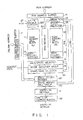
- Fig. 1 is a block diagram showing the entire circuit construction of a NOR type mask ROM according to one embodiment of this invention.
- the mask ROM of this invention is featured in that a main memory cell array having a plurality of mask ROM cells therein is divided into a plurality of blocks in the word line direction.
- main memory cell array is divided into two blocks 11 and 12 in the word line direction.
- Main memory cells are arranged in a matrix form in each of main memory cell blocks 11 and 12.
- the main memory cells arranged on the same row are connected to a corresponding one of word lines and the main memory cells arranged on the same column are connected to a corresponding one of bit lines.
- Word lines on the corresponding rows in main memory blocks 11 and 12 are selectively driven in parallel by means of row decoder 13.
- the output of row address buffer 14 which is supplied with an row address in supplied to row decoder 13.
- the bit lines in main memory cell blocks 11 and 12 are selected by means of main column decoders 15 and 16.
- the output of column address buffer and predecoder 17 which is supplied with a column address is supplied in parallel to main column decoders 15 and 16.
- One of the main memory cells in corresponding columns of main memory cell blocks 11 and 12 are selected according to the decoded outputs of row decoder 13-1 and main column decoders 15 and 16.
- Main/spare selector 18 is connected to main column decoders 15 and 16.
- the memory data of a main memory cell selected by main column decoders 15 and 16 are supplied to sense amplifier group 19 having a plurality of sense amplifier circuits via selector 18.
- Spare memory cells of the same number of main memory cells of each row in main memory cell blocks 11 and 12 are arranged on each of a plurality of rows in spare memory cell group 20.
- the spare memory cells may be PROMs or fuses into which given ROM data can be programmed.
- ROM data programming with respect to the memory cells in spare memory cell group 20 is effected by use of the output of programming decoder 21.
- Programming decoder 21 is supplied with the output of write-in address buffer 22 which is supplied with a write-in address.
- ROM data programmed into the memory cells of spare memory cell group 20 can be selected for each row according to a signal of spare row line SWL.
- spare column decoder 23 One bit included in ROM data of the spare memory cells of a selected row is selected for each output bit by means of spare column decoder 23 which is supplied with the output of column address buffer and predecoder 17.
- Spare column decoder 23 is also connected to spare/main selector 24, and one-bit data from one of the spare memory cells in spare memory cell group 20 selected for each output bit by spare column decoder 23 is supplied to sense amplifier group 19 via selector 24.
- the operation of spare/main selector 24 and main/spare selector 18 is controlled by a signal of block selector signal line BSL. Data read out from a main memory cell in main memory cell blocks 11 and 12 or a spare memory cell or spare memory cell group 20 is output via sense amplifier group 19.
- Spare row decoder 25 is supplied with the output of row address buffer 14. Programmable elements such as PROMs or fuses in which information can be programmed are arranged in spare row decoder 25. That part of the ROM data which is to be replaced or defection row addresses are written into the programmable elements. Spare row decoder 25 compares the previously programmed defective row address with the output row address of row address buffer 14, and supplies an output signal for selecting the row in spare memory cell group 20 to spare row line SWL based on the comparison result.
- Block selector 26 is supplied with a decoded output of spare row decoder 25.
- Information programmable elements are also arranged in block selector 26, and address information for identifying either one of main memory cell blocks 11 and 12 is programmed into the programmable elements.
- the data output from spare row decoder 25 is written into block selector 26.
- Selector 26 compares this data with the input address information, and generates a signal for controlling main/spare selector 18 spare/main selector 24 from the results of the comparison.
- the output signal of selector 26 is supplied to block selector signal line BSL.
- Write enable circuit 27 is operated in response to write-in control signal WCS supplied from the exterior of the device. When write-in control signal WCS is supplied, write enable circuit 27 outputs signal WE which permits data or address to be programmed into the spare memory cell of spare memory cell group 20, memory cell of spare row decoder 25 and memory cell of block selector 26.
- write-in control signal WCS is supplied from the exterior to operate write enable circuit 27.
- the defective memory cells may include not only main memory cells which are themselves defective but also main memory cells which are connected to broken or cutoff word lines, for example.
- Output signal WE of write enable circuit 27 permits data or address to be programmed into the spare memory cell of spare memory cell group 20, programmable element of spare row decoder 25 and programmable element of block selector 26.
- a row address designating the defective main memory cells of one row is programmed into spare row decoder 25, and data indicating that one of main memory cell blocks 11 and 12 which contains the defective memory cells is programmed into block selector 26. Then, the write-in address is supplied to write-in address buffer 22, decoded by write-in decoder 21, and supplied to spare memory cell group 20. In this condition, correct data to be stored in the defective main memory cells of one row are programmed into the spare memory cells of one row in spare memory cell group 20.
- row and column addresses are supplied.
- One main memory cell is selected for each output bit in a row of main memory cell blocks 11 and 12 by means of row decoder 13-1 and main column decoders 15 and 16 according to the input addresses.
- the memory data of the selected main memory cell is supplied to main/spare selector 18.
- main/spare selector 18 is operated by the output of block selector 26, and the readout ROM data from the selected cell is input to sense amplifier group 19. After this, ROM data amplified by sense amplifier group 19 is output to the exterior.
- spare column decoder 23 selects a bit corresponding to the column address input from the ROM data of one row, and supplies the selected bit to spare/main selector 24.
- main/spare selector 18 is set non-operative and spare/main selector 24 is set operative by the present output of block selector 26.
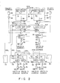
- Fig. 2 is a circuit diagram showing the detail construction of main portions of the mask ROM according to the first embodiment shown in Fig. 1.
- Word lines 31 and 32 are respectively arranged in main memory cell blocks 11 and 12.
- the decoded output of each of NAND gates 33 is supplied to corresponding word lines 31 and 32 via inverters 34 and 35. respectively.
- Each NAND gate 33 is a decoding portion for one of the rows in row decoder 13-1 and is supplied with the row address.
- Inverters 34 and 35 function as buffers for supplying the decoded output of NAND gate 33 to word lines 31 and 32.
- Bit lines 36 and 37 are respectively arranged in main memory cell blocks 11 and 12.
- One end of the current path of each of decoding transistors 38 arranged in main column decoder 15 is connected to corresponding bit line 36, and one end of the current path of each of decoding transistors 39 arranged in main column decoder 16 is connected to corresponding bit line 37.
- One end of the current path of each of selection transistors 40L arranged in main/spare selector 18 is connected to the other end of the current path of a corresponding one of decoding transistors 38, and one end of the current path of each of selection transistors 40R arranged in main/spare selector 18 is connected to the other end of the current path of a corresponding one of decoding transistors 39.
- each selection transistor 40L The other end of the current path of each selection transistor 40L is connected to sense amplifier circuit 41L provided in sense amplifier group 19, and the other end of the current path of each selection transfer 40R is connected to sense amplifier circuit 41R provided in sense amplifier group 19. Also, sense amplifier circuit 41L is connected to one end of the current path of each of selection transistors 42L provided in spare/main selector 24, and sense amplifier circuit 41R is connected to one end of the current path of each of selection transistors 42R provided in spare/main selector 24.
- each selection transistor 42L is connected to one end of the current path of a corresponding one of decoding transistors 43 arranged in spare column decoder 23, and the other end of the current path of each selection transistor 42R is connected to one end of the current path of a corresponding one of decoding transistors 44 arranged in spare column decoder 23.
- NAND gates 45 and 47 acting as predecoders in column address buffer and predecoder 17 are supplied with the column address input.
- the decoded output of each NAND gate 45 is supplied to the gates of corresponding transistors 38 and 43 via inverter 46 acting as a buffer, and the decoded output of each NAND gate 47 is supplied to the gates of corresponding transistors 39 and 44 via inverter 48 acting as a buffer.
- Spare memory cells 51 of a plurality of rows are arranged in spare memory cell group 20. Spare memory cells 51 in each row are selected by signals of corresponding spare row lines SWL.
- the ROM data write-in operations for spare memory cells 51 is respectively effected by the outputs supplied from NAND gates 52 constituting partial decoders in write-in decoder 21 via inverters 53 acting as a buffer. NAND gates 52 is supplied with write enable signal WE from write enable circuit 27.
- Spare memory cells 51 is respectively connected to the other ends of the current paths of corresponding transistors 43 and 44. With this connection, ROM data from spare memory cells 51 can be selectively supplied to sense amplifier circuits 41L and 41R via decoding transistors 43 and 44 and selection transistors 42L and 42R, respectively.
- a plurality of partial decoders 60 are arranged in spare row decoder 25. As shown in Fig. 2, each of partial decoders 60 includes load P-channel MOS transistor 62 connected to output node 61 and a plurality of programmable elements 63. The potential of output node 61 is supplied to a corresponding one of spare row lines SWL and to block selector 26. The operation of writing address information into programmable elements 63 in partial decoder 60 is effected in response to the outputs of NAND gates 65 via respective inverters 66 acting as a buffer. NAND gates 65 are each supplied with a write-in address and write enable signal WE from write enable circuit 27.
- a plurality of partial decoders 70 are arranged in block selector 26.
- Each partial selector 70 includes load P-channel MOS transistor 72 connected to output node 71, a plurality of programmable elements 73, and inverter 74 connected to output node 71.
- the output of inverter 74 in each partial decoder 70 is supplied to a corresponding one of block selector signal lines BSL.
- the signals of block selector signal lines BSL are supplied directly to the gates of respective transistors 42L and 42R of spare/main selector 24 and to the gates of transistor 40L and 40R of main/spare selector 18 via respective inverters 81.
- each NAND gate 75 is supplied with a write-in address and write enable signal WE generated from write enable circuit 27.
- transistors whose channel type is not specified are of N-channel type.
- spare memory cells 51 of one row are selected by a signal of a corresponding one of spare word lines SWL, and the previously programmed ROM data is read out from each spare memory cell 51.
- the signal of spare word line SWL is also supplied to a corresponding one of partial decoders 70 of block selector 26.
- the output of partial decoder 70 of block selector 26 supplied with the signal of spare word line SWL also becomes "1" level, and the decoded output is supplied to turn on a corresponding one of transistors 42L of spare/main selector 24 and turn off a corresponding one of transistors 40L of main/spare selector 18.
- data of corresponding spare memory cell 51 is supplied instead of ROM cell data of main memory cell block 11 to sense amplifier circuit 41L via transistor 43 of spare column decoder 23 and transistor 42L of spare/main selector 24.
- the main memory cell array is divided into two blocks and the number of main memory cells connected to each word line is reduced.
- the number of spare memory cells connected to the same word line of spare memory cell group 20 for compensating for defective memory cells can be reduced.
- an increase in the chip size can be suppressed to a minimum even if the redundancy function is added.
- the main memory cell array is divided into two blocks, but can be divided into three or more blocks.
- An increase in the number of divided blocks allows the number of spare memory cells connected to the same word line in spare memory cell group 20 to be reduced, thus suppressing the increase in the chip size to a minimum.
- spare memory cells of two rows in spare memory cell group 20 are used instead of the memory cells connected to the shorted word lines in order to compensate for the defective rows.
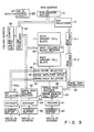
- Fig. 3 shows the entire circuit construction of a mask ROM according to another embodiment of this invention
- Fig. 4 shows main portions of the circuit of Fig. 3.
- the main memory cell array is divided into a plurality of (two) blocks in a row direction, and spare memory cells can be easily replaced by the main memory cells in order to compensate for the defective memory cells caused by the defective word line or lines.
- bit lines may be cut off or shorted.
- the main memory cell array in the circuit of Figs. 3 and 4 is divided into a plurality of (two) blocks in a bit line direction so that two divided main memory cell arrays can be obtained.
- Fig. 3 the same portions as those in Fig. 1 are denoted by the same reference numerals.
- Word lines (not shown) are selectively driven by row decoders 13-1 and 13-2.
- Row decoders 13-1 and 13-2 are supplied with the output of row predecoder 13 to which an output of row address buffer 14 is supplied.
- Row address is supplied to a row address buffer 14.
- the bit lines (not shown) of main memory cell blocks 11 and 12 are selected by main column and block decoder 85 disposed between main memory cell blocks 11 and 12.
- the column and block decoder 85 is used to determine whether the upper block (main memory cell block 11) or the lower block (main memory cell block 12) should be selected, or determine which columns of memory cells should be selected to bits from the memory cells of these columns.
- Main column and block decoder 85 is supplied with the output of column predecoder 87 to which an output of column address buffer 86 and an output of row address buffer 14 is supplied.
- Column address supplied to a column address buffer 86.
- the memory data of the main memory cell selected by means of main column and block decoder 85 is supplied to sense amplifier group 19 having a plurality of sense amplifier circuits via main/spare selector 18.
- Spare memory cell group 20 has a spare memory cells such as PROM spare cells or fuses in which information can be programmed.
- the number of the spare memory cells of each column is the same as that of the main memory cells of each column in main memory cell blocks 11 and 12.
- the operation of programming ROM data into each spare memory cell of spare memory cell group 20 is effected in response to the output of write-in decoder 21.
- Write-in decoder 21 is supplied with the output of write-in address buffer 22 to which a write-in address is supplied.
- Data programmed in the spare memory cells of spare memory cell group 20 is selected for each row in response to a signal of data line selector line DSL connected to spare row/column decoder 28.
- Spare row/column decoder 28 has programmable elements in which information can be programmed and to which the output of write-in decoder 29 is supplied.
- Write-in decoder 29 is supplied with the output of write-in address buffer 30 to which column address information corresponding to the defective column indicating address is supplied.
- An output of the row predecoder 13 is supplied to an spare predecoder 90.
- An output of the spare predecoder 90 is supplied to the spare row decoder 25.
- the spare row decoder 25 selects one bit from the correct ROM data of the spare memory cells of one column selected in spare memory cell group 20.
- Spare row decoder 25 is connected to spare/main selector 24, and correct ROM data of one bit in spare memory cell group 20 corresponding to a column selected by spare row/column decoder 28 is supplied to sense amplifier group 19 via selector 24.
- the operation of spare/main selector 24 and main/spare selector 18 is controlled by a signal of bit selector signal line BSL.
- Bit selector 10 is supplied with the output of spare row/column decoder 28. Also, programmable elements in which information be programmed are arranged in bit selector 10. Data designating one or main memory cell blocks 11 and 12 is programmed into the programmable elements by means of write-in decoder 9 and write-in address buffer 8. The data output from spare row/column detector 28 is written into bit selector 10. Selector 10 compares this data with the input address information, and generates a signal for controlling main/spare selector 18 and spare/main selector 22 from the results of the comparison. The output signal of selector 26 is supplied to bit selector signal line BSL.
- Write enable circuit 27 generates, in response to externally supplied write-in control signal WCS, signal WE which permits ROM data or addresses to be programmed into spare memory cells of spare memory cell group 20, programmable elements of spare row/column decoder 28 and programmable elements of bit selector 10.
- write-in control signal WCS is supplied from the exterior to operate write enable circuit 27.
- the spare memory cells in spare memory cell group 20, programmable elements in spare row/column decoder 28 and programmable elements in bit selector 10 are set into an operative condition in which ROM data or addresses can be programmed.
- the defective main memory cells may include not only main memory cells which are themselves damaged but also main memory cells connected to broken or cutoff bit lines, for example.
- a row and column address designating the row and column of defective main memory cells are programmed into spare row/column decoder 28 and output bit address information indicating that one of main memory cell blocks 11 and 12 which contains the defective main memory cells is programmed into bit selector 10.
- main memory cell In the ROM data readout mode, row and column addresses are supplied.
- One main memory cell is selected for each output bit in a column of main memory cell blocks 11 and 12 by means of row decoders 13-1, 13-2 and main column and block decoder 85 according to the input addresses.
- the memory data of the selected main memory cell is supplied to main/spare selector 18.
- main/spare selector 18 is operated by the output of bit selector 10, and the readout ROM data from the selected cell is input to sense amplifier group 19. After this, the readout ROM data is output to the exterior.
- spare row decoder 25 select a bit to the row address input from the address information of one column, and supplies the selected bit to spare/main selector 24.
- main/spare selector 18 is set non-operative and spare/main selector 24 is set operative by the present output of bit selector 10.
- data of the bit selected by spare row decoder 25 is supplied from spare/main selector 24 to sense amplifier group 19 instead of ROM data stored in the defective main memory cells of the main memory cell array, and then the correct ROM data can be supplied to the exterior.
- Fig. 4 is a circuit diagram showing the detail construction of main portions of the mask ROM shown in Fig. 3.
- Bit lines 131L and 131R are respectively arranged in main memory cell block 11 and bit lines 132L and 132R are respectively arranged in main memory cell block 12.
- NAND gate 133 functioning as a decoder portion for one column in main column and block decoder 85 is supplied with the most significant bit of the row address and the column address.
- the predecoded output of NAND gate 133 is supplied to the gates of transistors 136 constituting main column and block decoder 85 via inverter 134 acting as a buffer. Selection transistors 136 are arranged in main column and block decoder 85.
- each of transistors 136 is connected at one end to a corresponding one of the output terminals of main column and block decoder 85.
- Sense amplifier circuits 138L and 138R are disposed in sense amplifier group 19 and connected to the other ends of the current paths of transistors 137L and 137R, respectively.
- Selection transistors 137L and 137R are arranged in main/spare selector 18.
- Selection transistors 139L and 139R are arranged in spare/main selector 24, and the current paths thereof are connected at one end to respective sense amplifier circuits 138L and 138R.
- Decoding transistors 140 are arranged in spare row decoder 25, and the current paths thereof are connected at one end to the other ends of the current paths of transistors 139L and 139R, respectively outputs of spare row predecoder 90 are supplied with respective gates of decoding transistors 140.
- Spare row predecoder 90 is composed of inverter 92 and NAND decoder 91.
- NAND decoder 91 is supplied with the output of row predecoder 13.
- Inverter 92 is a buffer that is supplied with the output of NAND decoder 91.
- NAND gates 141 are decoders in row decoder 13-1 and 13-2.
- Inverters 142 acting as buffers are supplied with respective decoded outputs of NAND gates 141, and the outputs of inverters 142 are supplied to the respective bit lines.
- a plurality of columns of spare memory cells 143 are arranged in spare memory cell group 20.
- the operation of programming data into spare memory cells 143 is effected in response to the outputs supplied from partial decoders or NAND gates 144 arranged in write-in decoder 21 via respective inverters 145.
- Data of each spare memory cell 143 is selectively supplied to a corresponding one of sense amplifier circuits 138L and 138R via transistors 140, 139L and 139R.
- Each NAND gate 144 is supplied with a corresponding write-in address and write enable signal WE output from write enable circuit 27.
- a plurality of partial decoders 146L, 146R are arranged in bit selector 10.
- Each partial decoder 146L, 146R includes load P-channel MOS transistor 148 connected to node 147, a plurality of programmable elements 149, and inverter 150 whose input terminal is connected to node 147.
- the output of inverter 150 of each partial decoder 146L, 146R are output to a corresponding one of bit selector signal lines BSL.
- a signal of each bit selector signal line BSL is supplied directly to the gate of a corresponding one of transistors 139L, 139R in spare/main selector 24 and to the gate of a corresponding one of transistors 137L, 137R in main/spare selector 18 via inverter 151L, 151R.
- the operation of programming information into each programmable elements 149 of partial decoder 146R is effected in response to the output of a corresponding one of NAND gates 152 supplied via inverters 153 acting as a buffer.
- Each NAND gate 152 is supplied with a write address and write enable signal WE from write enable circuit 27.
- a plurality of partial decoders 154 are provided in spare row/column decoder 28.
- each partial decoder 154 includes load P-channel MOS transistor 156 connected to output node 155 and a plurality of programmable elements 157.
- the potential of output node 155 is supplied to corresponding data line selector line DSL and bit selector 10.
- the operation of programming data into each programmable element 157 of partial decoder 154 is effected by use of the output of a corresponding one of NAND gates 158 which is supplied via inverter 159 acting as a buffer.
- Each NAND gate 158 is supplied with a write address and write enable signal WE form write enable circuit 27.
- transistors whose channel type is not specified are of N-channel type.
- a row address (the most significant bit thereof, for example) and a column address are supplied to spare row/column decoder 28.
- the row address is used to select the upper or lower block
- the column address is used to select one of the columns.
- the most significant bit of the input row address coincides with the previously programmed data
- the input column and row addresses coincide with the previously programmed column and row addresses and the decoded output of one of partial decoders 154 in spare row/column decoder 28 is at "1" level.
- a column of spare memory cells 143 is selected by a signal of a corresponding one of data line selector lines DSL so that previously programmed ROM data can be read out from each spare memory cell 143.
- a signal of data line selector signal line DSL is also supplied to partial decoders 146L and 146R of bit selector 10.
- bit line 132L output bit L
- the decoded output of partial decoder 146L of bit selector 10 which is supplied with signals of a plurality of data selector signal lines DLS becomes "1" level.
- transistor 139L of spare/main selector 24 which is supplied with the decoded output is turned on and transistor 137L of main/spare selector 18 is turned off.
- the decoded output of partial decoder 146R of bit selector 10 becomes "0" level, and as a result, transistor 139R of spare/main selector 24 which is supplied with the decoded output is turned off and transistor 137R of main/spare selector 18 is turned on. That is, in this case, instead of ROM data of the main memory cells of one column on bit line 132L on the side of output bit L, ROM data of spare memory cells 143 is supplied to sense amplifier circuit 138L via transistor 140 of spare row decoder 25 and transistor 139L of spare/main selector 24 in this order. Thus, the main memory cells connected to the defective bit line of the main memory cell array can be compensated for or ROM data can be replaced.
- ROM data of spare memory cells 143 is supplied to sense amplifier circuit 138R via transistor 140 of spare row decoder 25 and transistor 139R of spare/main selector 24 in this order.
- the defective memory cells caused by the damaged memory cell or cutoff bit line are compensated for.
- spare memory cells of two columns or corresponding number of columns in spare memory cell group 20 may be used instead of the defective memory cell columns.
- the above description is limited to the measures taken in the case where at least one cell of the main memory is found to be defective. Nonetheless, the present invention can apply to the case where part of the data stored in the ROM needs to be altered even if no memory cells have been found to be defective.
- the data stored in a certain storage area of the main memory can be altered at once by simultaneously selecting the rows and columns of cells, which define that area, by means of the bit selector and the block selector.
- the main memory cell array is divided into two blocks, but it can be divided into three or more blocks. As the number of divided blocks increases, the number of spare memory cells of each column in spare memory cell group 20 can be further reduced, preventing the chip size from increasing.
Landscapes
- Engineering & Computer Science (AREA)
- Microelectronics & Electronic Packaging (AREA)
- Computer Hardware Design (AREA)
- For Increasing The Reliability Of Semiconductor Memories (AREA)
- Read Only Memory (AREA)
Applications Claiming Priority (2)
| Application Number | Priority Date | Filing Date | Title |
|---|---|---|---|
| JP66535/88 | 1988-03-18 | ||
| JP6653588 | 1988-03-18 |
Publications (3)
| Publication Number | Publication Date |
|---|---|
| EP0333207A2 true EP0333207A2 (de) | 1989-09-20 |
| EP0333207A3 EP0333207A3 (de) | 1990-12-27 |
| EP0333207B1 EP0333207B1 (de) | 1997-06-11 |
Family
ID=13318685
Family Applications (1)
| Application Number | Title | Priority Date | Filing Date |
|---|---|---|---|
| EP89104787A Expired - Lifetime EP0333207B1 (de) | 1988-03-18 | 1989-03-17 | Masken-rom mit Ersatzspeicherzellen |
Country Status (4)
| Country | Link |
|---|---|
| US (1) | US5124948A (de) |
| EP (1) | EP0333207B1 (de) |
| KR (1) | KR910008694B1 (de) |
| DE (1) | DE68928112T2 (de) |
Cited By (6)
| Publication number | Priority date | Publication date | Assignee | Title |
|---|---|---|---|---|
| EP0472209A3 (en) * | 1990-08-23 | 1992-12-23 | Kabushiki Kaisha Toshiba | Semiconductor memory device having redundant circuit |
| EP0383452A3 (de) * | 1989-01-31 | 1992-12-23 | Fujitsu Limited | Halbleiterspeicher mit einer Einrichtung zum Ersetzen defekter Speicherzellen |
| EP0657814A1 (de) * | 1993-12-07 | 1995-06-14 | STMicroelectronics S.r.l. | Halbleiterspeicher mit redundanter Schaltung |
| EP0586114A3 (en) * | 1992-08-31 | 1996-10-16 | Sharp Kk | A semiconductor read only memory |
| US5764575A (en) * | 1995-09-29 | 1998-06-09 | Sharp Kabushiki Kaisha | Replacement semiconductor read-only memory |
| WO2002039457A3 (de) * | 2000-11-07 | 2002-09-19 | Infineon Technologies Ag | Speicherverwaltungslogik zur erweiterten nutzung von festwertspeichern |
Families Citing this family (49)
| Publication number | Priority date | Publication date | Assignee | Title |
|---|---|---|---|---|
| US5426607A (en) * | 1988-04-27 | 1995-06-20 | Sharp Kabushiki Kaisha | Redundant circuit for memory having redundant block operatively connected to special one of normal blocks |
| KR910005601B1 (ko) * | 1989-05-24 | 1991-07-31 | 삼성전자주식회사 | 리던던트 블럭을 가지는 반도체 메모리장치 |
| JP2630059B2 (ja) * | 1990-11-09 | 1997-07-16 | 日本電気株式会社 | 半導体メモリ装置 |
| KR960010736B1 (ko) * | 1991-02-19 | 1996-08-07 | 미쓰비시뎅끼 가부시끼가이샤 | 마스크 rom 및 그 제조방법 |
| US5257229A (en) * | 1992-01-31 | 1993-10-26 | Sgs-Thomson Microelectronics, Inc. | Column redundancy architecture for a read/write memory |
| JP2501993B2 (ja) * | 1992-02-24 | 1996-05-29 | 株式会社東芝 | 半導体記憶装置 |
| KR960002777B1 (ko) * | 1992-07-13 | 1996-02-26 | 삼성전자주식회사 | 반도체 메모리 장치의 로우 리던던시 장치 |
| JP2816512B2 (ja) * | 1992-07-27 | 1998-10-27 | 三菱電機株式会社 | 半導体記憶装置 |
| US5386380A (en) * | 1993-07-21 | 1995-01-31 | United Microelectronics Corporation | Bypass scheme for ROM IC |
| JP3215237B2 (ja) * | 1993-10-01 | 2001-10-02 | 富士通株式会社 | 記憶装置および記憶装置の書き込み/消去方法 |
| KR960008825B1 (en) * | 1993-11-18 | 1996-07-05 | Samsung Electronics Co Ltd | Row redundancy circuit and method of semiconductor memory device with double row decoder |
| IN188196B (de) * | 1995-05-15 | 2002-08-31 | Silicon Graphics Inc | |
| JP3557022B2 (ja) * | 1995-12-08 | 2004-08-25 | 株式会社東芝 | 半導体記憶装置 |
| US5841709A (en) * | 1995-12-29 | 1998-11-24 | Stmicroelectronics, Inc. | Memory having and method for testing redundant memory cells |
| US5771195A (en) * | 1995-12-29 | 1998-06-23 | Sgs-Thomson Microelectronics, Inc. | Circuit and method for replacing a defective memory cell with a redundant memory cell |
| US5790462A (en) * | 1995-12-29 | 1998-08-04 | Sgs-Thomson Microelectronics, Inc. | Redundancy control |
| US5612918A (en) * | 1995-12-29 | 1997-03-18 | Sgs-Thomson Microelectronics, Inc. | Redundancy architecture |
| US6037799A (en) * | 1995-12-29 | 2000-03-14 | Stmicroelectronics, Inc. | Circuit and method for selecting a signal |
| JPH1064256A (ja) * | 1996-08-20 | 1998-03-06 | Sony Corp | 半導体記憶装置 |
| US5796662A (en) * | 1996-11-26 | 1998-08-18 | International Business Machines Corporation | Integrated circuit chip with a wide I/O memory array and redundant data lines |
| US5841710A (en) * | 1997-02-14 | 1998-11-24 | Micron Electronics, Inc. | Dynamic address remapping decoder |
| US6314527B1 (en) | 1998-03-05 | 2001-11-06 | Micron Technology, Inc. | Recovery of useful areas of partially defective synchronous memory components |
| US6332183B1 (en) | 1998-03-05 | 2001-12-18 | Micron Technology, Inc. | Method for recovery of useful areas of partially defective synchronous memory components |
| US6381708B1 (en) | 1998-04-28 | 2002-04-30 | Micron Technology, Inc. | Method for decoding addresses for a defective memory array |
| US6381707B1 (en) | 1998-04-28 | 2002-04-30 | Micron Technology, Inc. | System for decoding addresses for a defective memory array |
| US6496876B1 (en) | 1998-12-21 | 2002-12-17 | Micron Technology, Inc. | System and method for storing a tag to identify a functional storage location in a memory device |
| JP2001143494A (ja) * | 1999-03-19 | 2001-05-25 | Toshiba Corp | 半導体記憶装置 |
| US6578157B1 (en) | 2000-03-06 | 2003-06-10 | Micron Technology, Inc. | Method and apparatus for recovery of useful areas of partially defective direct rambus rimm components |
| US7269765B1 (en) | 2000-04-13 | 2007-09-11 | Micron Technology, Inc. | Method and apparatus for storing failing part locations in a module |
| US6714467B2 (en) * | 2002-03-19 | 2004-03-30 | Broadcom Corporation | Block redundancy implementation in heirarchical RAM's |
| US20020199130A1 (en) * | 2001-06-20 | 2002-12-26 | Yao-Jung Kuo | Automatic address redirecting memory device and the method of the same |
| JP4639030B2 (ja) * | 2002-11-18 | 2011-02-23 | パナソニック株式会社 | 半導体記憶装置 |
| JP4424952B2 (ja) * | 2003-09-16 | 2010-03-03 | 株式会社ルネサステクノロジ | 不揮発性半導体記憶装置 |
| US6930934B2 (en) * | 2003-10-28 | 2005-08-16 | Taiwan Semiconductor Manufacturing Co., Ltd. | High efficiency redundancy architecture in SRAM compiler |
| CN101221816B (zh) * | 2007-01-12 | 2013-04-24 | 张国飙 | 具有预留空间的掩膜编程存储器 |
| US8041989B2 (en) * | 2007-06-28 | 2011-10-18 | International Business Machines Corporation | System and method for providing a high fault tolerant memory system |
| US8041990B2 (en) * | 2007-06-28 | 2011-10-18 | International Business Machines Corporation | System and method for error correction and detection in a memory system |
| KR101282967B1 (ko) * | 2007-09-21 | 2013-07-08 | 삼성전자주식회사 | 리던던시 메모리 블록을 가지는 반도체 메모리 장치 및그의 셀 어레이 구조 |
| TWI375959B (en) * | 2007-11-06 | 2012-11-01 | Nat Univ Tsing Hua | Method for repairing memory and system thereof |
| US8050075B2 (en) * | 2007-11-07 | 2011-11-01 | Semiconductor Components Industries, Llc | Memory |
| WO2010119520A1 (ja) * | 2009-04-15 | 2010-10-21 | ルネサスエレクトロニクス株式会社 | マスクromの製造に向けられたレイアウトパターンを作成するためのシステム、そのシステムを用いて製造されたマスクrom、およびマスクパターンを作成するための方法 |
| US8631271B2 (en) | 2010-06-24 | 2014-01-14 | International Business Machines Corporation | Heterogeneous recovery in a redundant memory system |
| US8549378B2 (en) | 2010-06-24 | 2013-10-01 | International Business Machines Corporation | RAIM system using decoding of virtual ECC |
| US8484529B2 (en) | 2010-06-24 | 2013-07-09 | International Business Machines Corporation | Error correction and detection in a redundant memory system |
| US8898511B2 (en) | 2010-06-24 | 2014-11-25 | International Business Machines Corporation | Homogeneous recovery in a redundant memory system |
| US8522122B2 (en) | 2011-01-29 | 2013-08-27 | International Business Machines Corporation | Correcting memory device and memory channel failures in the presence of known memory device failures |
| CN105990362A (zh) * | 2015-02-10 | 2016-10-05 | 成都海存艾匹科技有限公司 | 具有预留空间的三维掩膜编程只读存储器 |
| CN108735268B (zh) * | 2017-04-19 | 2024-01-30 | 恩智浦美国有限公司 | 非易失性存储器修复电路 |
| KR102492033B1 (ko) * | 2018-03-26 | 2023-01-26 | 에스케이하이닉스 주식회사 | 메모리 장치 및 이를 포함하는 메모리 시스템 |
Family Cites Families (27)
| Publication number | Priority date | Publication date | Assignee | Title |
|---|---|---|---|---|
| JPS5721799B2 (de) * | 1975-02-01 | 1982-05-10 | ||
| DE2621399A1 (de) * | 1975-05-29 | 1976-12-09 | Int Standard Electric Corp | Speichereinrichtung |
| US4281398A (en) * | 1980-02-12 | 1981-07-28 | Mostek Corporation | Block redundancy for memory array |
| JPS56157056A (en) * | 1980-05-09 | 1981-12-04 | Fujitsu Ltd | Manufacture of read-only memory |
| US4389715A (en) * | 1980-10-06 | 1983-06-21 | Inmos Corporation | Redundancy scheme for a dynamic RAM |
| US4385368A (en) * | 1980-11-24 | 1983-05-24 | Raytheon Company | Programmable read only memory |
| US4489402A (en) * | 1981-04-25 | 1984-12-18 | Tokyo Shibaura Denki Kabushiki Kaisha | Semiconductor memory device |
| JPS582943A (ja) * | 1981-06-30 | 1983-01-08 | Toshiba Corp | メモリ拡張代替方式 |
| US4400798A (en) * | 1981-07-13 | 1983-08-23 | Tektronix, Inc. | Memory patching system |
| US4422161A (en) * | 1981-10-08 | 1983-12-20 | Rca Corporation | Memory array with redundant elements |
| JPS58188155A (ja) * | 1982-04-27 | 1983-11-02 | Seiko Epson Corp | 2層構造rom集積回路 |
| US4493075A (en) * | 1982-05-17 | 1985-01-08 | National Semiconductor Corporation | Self repairing bulk memory |
| JPS595497A (ja) * | 1982-07-02 | 1984-01-12 | Hitachi Ltd | 半導体rom |
| JPS5919367A (ja) * | 1982-07-26 | 1984-01-31 | Toshiba Corp | メモリ付ゲ−トアレイ |
| GB2129585B (en) * | 1982-10-29 | 1986-03-05 | Inmos Ltd | Memory system including a faulty rom array |
| JPH0670880B2 (ja) * | 1983-01-21 | 1994-09-07 | 株式会社日立マイコンシステム | 半導体記憶装置 |
| US4556975A (en) * | 1983-02-07 | 1985-12-03 | Westinghouse Electric Corp. | Programmable redundancy circuit |
| US4601019B1 (en) * | 1983-08-31 | 1997-09-30 | Texas Instruments Inc | Memory with redundancy |
| JPH0666120B2 (ja) * | 1983-11-09 | 1994-08-24 | 株式会社東芝 | 半導体記憶装置の冗長部 |
| GB2154032B (en) * | 1984-02-08 | 1988-04-20 | Inmos Ltd | A repairable memory array |
| US4599709A (en) * | 1984-02-17 | 1986-07-08 | At&T Bell Laboratories | Byte organized static memory |
| US4610000A (en) * | 1984-10-23 | 1986-09-02 | Thomson Components-Mostek Corporation | ROM/RAM/ROM patch memory circuit |
| JPS61123169A (ja) * | 1984-11-20 | 1986-06-11 | Fujitsu Ltd | 半導体集積回路 |
| JPH0611072B2 (ja) * | 1985-08-21 | 1994-02-09 | 三菱電機株式会社 | 半導体不揮発性記憶装置 |
| JPS62121979A (ja) * | 1985-11-22 | 1987-06-03 | Mitsubishi Electric Corp | 集積回路メモリ |
| JPS62293598A (ja) * | 1986-06-12 | 1987-12-21 | Toshiba Corp | 半導体記憶装置 |
| US4807191A (en) * | 1988-01-04 | 1989-02-21 | Motorola, Inc. | Redundancy for a block-architecture memory |
-
1989
- 1989-03-17 EP EP89104787A patent/EP0333207B1/de not_active Expired - Lifetime
- 1989-03-17 DE DE68928112T patent/DE68928112T2/de not_active Expired - Fee Related
- 1989-03-18 KR KR1019890003384A patent/KR910008694B1/ko not_active Expired
-
1991
- 1991-08-22 US US07/751,574 patent/US5124948A/en not_active Expired - Lifetime
Cited By (10)
| Publication number | Priority date | Publication date | Assignee | Title |
|---|---|---|---|---|
| EP0383452A3 (de) * | 1989-01-31 | 1992-12-23 | Fujitsu Limited | Halbleiterspeicher mit einer Einrichtung zum Ersetzen defekter Speicherzellen |
| EP0686980A1 (de) * | 1989-01-31 | 1995-12-13 | Fujitsu Limited | Halbleiterspeicher mit Einrichtung zum Ersetzen defekter Speicherzellen |
| EP0472209A3 (en) * | 1990-08-23 | 1992-12-23 | Kabushiki Kaisha Toshiba | Semiconductor memory device having redundant circuit |
| US5272672A (en) * | 1990-08-23 | 1993-12-21 | Kabushiki Kaisha Toshiba | Semiconductor memory device having redundant circuit |
| EP0586114A3 (en) * | 1992-08-31 | 1996-10-16 | Sharp Kk | A semiconductor read only memory |
| EP0657814A1 (de) * | 1993-12-07 | 1995-06-14 | STMicroelectronics S.r.l. | Halbleiterspeicher mit redundanter Schaltung |
| US5566114A (en) * | 1993-12-07 | 1996-10-15 | Sgs-Thomson Microelectronics S.R.L. | Redundancy circuitry for a semiconductor memory device |
| US5764575A (en) * | 1995-09-29 | 1998-06-09 | Sharp Kabushiki Kaisha | Replacement semiconductor read-only memory |
| WO2002039457A3 (de) * | 2000-11-07 | 2002-09-19 | Infineon Technologies Ag | Speicherverwaltungslogik zur erweiterten nutzung von festwertspeichern |
| US6874073B2 (en) | 2000-11-07 | 2005-03-29 | Infineon Technologies Ag | Method for managing data stored primarily in a read-only memory |
Also Published As
| Publication number | Publication date |
|---|---|
| KR890015280A (ko) | 1989-10-28 |
| DE68928112T2 (de) | 1997-11-20 |
| DE68928112D1 (de) | 1997-07-17 |
| KR910008694B1 (ko) | 1991-10-19 |
| US5124948A (en) | 1992-06-23 |
| EP0333207A3 (de) | 1990-12-27 |
| EP0333207B1 (de) | 1997-06-11 |
Similar Documents
| Publication | Publication Date | Title |
|---|---|---|
| EP0333207A2 (de) | Masken-rom mit Ersatzspeicherzellen | |
| US5163023A (en) | Memory circuit capable of replacing a faulty column with a spare column | |
| KR940007241B1 (ko) | 반도체 메모리 장치의 로우 리던던시장치 | |
| US6865124B2 (en) | Semiconductor device with flexible redundancy system | |
| EP0313040B1 (de) | Löschbares programmierbares Festwertspeichergerät | |
| US5355339A (en) | Row redundancy circuit of a semiconductor memory device | |
| US5034925A (en) | Semiconductor memory device with redundancy responsive to advanced analysis | |
| US4648075A (en) | Redundancy circuit for a semiconductor memory device | |
| US5485424A (en) | Semiconductor memory and redundant-address writing method | |
| US5388076A (en) | Semiconductor memory device | |
| EP0252325B1 (de) | Halbleiteranordnung mit einer Schmelzsicherungsschaltung und einer Erkennungsschaltung, um Schmelzsicherungszustände in der Schmelzsicherungsschaltung zu erkennen | |
| EP0361404B1 (de) | Speicherschaltung mit verbesserter Redundanzstruktur | |
| US5122987A (en) | Semiconductor memory device with individually addressable space cells capable of driving a data bus | |
| KR900006160B1 (ko) | 반도체 기억 장치 | |
| EP0472209B1 (de) | Halbleiterspeichergerät mit Redundanzschaltung | |
| US4672581A (en) | Repairable memory array | |
| US5058071A (en) | Semiconductor memory device having means for repairing the memory device with respect to possible defective memory portions | |
| US4937790A (en) | Semiconductor memory device | |
| KR960011633B1 (ko) | 반도체 판독전용 메모리 | |
| JP3112018B2 (ja) | 冗長メモリを有する半導体記憶装置 | |
| KR0140350B1 (ko) | 반도체 기억 장치 | |
| EP0686980B1 (de) | Halbleiterspeicher mit Einrichtung zum Ersetzen defekter Speicherzellen | |
| KR0172382B1 (ko) | 메모리셀 어레이 블럭의 재배치가 가능한 반도체 메모리 장치 | |
| KR100317568B1 (ko) | 반도체기억장치 | |
| US4489402A (en) | Semiconductor memory device |
Legal Events
| Date | Code | Title | Description |
|---|---|---|---|
| PUAI | Public reference made under article 153(3) epc to a published international application that has entered the european phase |
Free format text: ORIGINAL CODE: 0009012 |
|
| 17P | Request for examination filed |
Effective date: 19890414 |
|
| AK | Designated contracting states |
Kind code of ref document: A2 Designated state(s): DE FR GB |
|
| PUAL | Search report despatched |
Free format text: ORIGINAL CODE: 0009013 |
|
| AK | Designated contracting states |
Kind code of ref document: A3 Designated state(s): DE FR GB |
|
| 17Q | First examination report despatched |
Effective date: 19930713 |
|
| GRAG | Despatch of communication of intention to grant |
Free format text: ORIGINAL CODE: EPIDOS AGRA |
|
| GRAH | Despatch of communication of intention to grant a patent |
Free format text: ORIGINAL CODE: EPIDOS IGRA |
|
| GRAH | Despatch of communication of intention to grant a patent |
Free format text: ORIGINAL CODE: EPIDOS IGRA |
|
| GRAA | (expected) grant |
Free format text: ORIGINAL CODE: 0009210 |
|
| AK | Designated contracting states |
Kind code of ref document: B1 Designated state(s): DE FR GB |
|
| REF | Corresponds to: |
Ref document number: 68928112 Country of ref document: DE Date of ref document: 19970717 |
|
| ET | Fr: translation filed | ||
| PGFP | Annual fee paid to national office [announced via postgrant information from national office to epo] |
Ref country code: GB Payment date: 19980309 Year of fee payment: 10 |
|
| PGFP | Annual fee paid to national office [announced via postgrant information from national office to epo] |
Ref country code: FR Payment date: 19980310 Year of fee payment: 10 |
|
| PLBE | No opposition filed within time limit |
Free format text: ORIGINAL CODE: 0009261 |
|
| STAA | Information on the status of an ep patent application or granted ep patent |
Free format text: STATUS: NO OPPOSITION FILED WITHIN TIME LIMIT |
|
| 26N | No opposition filed | ||
| PG25 | Lapsed in a contracting state [announced via postgrant information from national office to epo] |
Ref country code: GB Free format text: LAPSE BECAUSE OF NON-PAYMENT OF DUE FEES Effective date: 19990317 |
|
| GBPC | Gb: european patent ceased through non-payment of renewal fee |
Effective date: 19990317 |
|
| PG25 | Lapsed in a contracting state [announced via postgrant information from national office to epo] |
Ref country code: FR Free format text: LAPSE BECAUSE OF NON-PAYMENT OF DUE FEES Effective date: 19991130 |
|
| REG | Reference to a national code |
Ref country code: FR Ref legal event code: ST |
|
| PGFP | Annual fee paid to national office [announced via postgrant information from national office to epo] |
Ref country code: DE Payment date: 20070315 Year of fee payment: 19 |
|
| PG25 | Lapsed in a contracting state [announced via postgrant information from national office to epo] |
Ref country code: DE Free format text: LAPSE BECAUSE OF NON-PAYMENT OF DUE FEES Effective date: 20081001 |